
Submitted:
16 November 2023
Posted:
21 November 2023
You are already at the latest version
Abstract
This study presents the design and implementation of a PLC microprocessor adhering to the IEC-61131-3 standard, executed on a Cyclone-V FPGA using a DE10-NANO development board. Our microprocessor optimizes the central processing unit by streamlining the data path, achieving a remarkable simulated response time of approximately 60 ns, equivalent to three clock cycles at a 50MHz frequency for Boolean operations. To substantiate our approach, we conducted practical experiments utilizing a FESTO conveyor station, employing relays as actuators, and incorporating optical and inductive sensors. The results underscore the feasibility of our proposed approach and serve as practical validation of its efficacy. This work introduces a promising avenue for the development of cost-effective PLCs employing SoC FPGA variants. Additionally, a thorough comparison of execution times with other early reported architectures. Our microprocessor outperforms even well-established PLCs like the S7-312, with substantial reductions in execution times of 94.54% for floating-point operations, 71.42% to 93.33% for word operations, and up to 78.57% for bit operations.
Keywords:
Architecture design
; FPGA
; IEC 61131-3
; low-latency
; PLC
; System-on-Chip
1. Introduction
A programmable Logic Controller (PLC) is a type of industrial automation technology widely used in harsh operating environments because of its ability to perform reliably under extreme conditions, such as high temperatures, humidity, strong vibrations, and electrical interference [1–3]. PLCs are typically programmed using the IEC 61131-3 standard, which defines a set of programming languages, instructions, syntax, and semantics [4,5]. However, the internal configuration of the PLC’s microprocessor can generate significant latency, which affects the efficiency of instruction execution [6,7]. In industrial applications, speed and reliability are critical, so it is essential to have Central Processing Units (CPU) working as efficiently as possible, allowing more complex algorithms to control processes faster and more precisely [8–11]. To address these issues, modern PLCs employ a System-On-Chip (SoC) approach that leverages hardware description languages (HDLs) to model, synthesize, and quickly reconfigure Field-Programmable Gate Array (FPGA) structures [9,10]. So, the designing of a PLC microprocessor can be approached in various ways:
For example, a code proposed in a programming language for the IEC61131-3 standard can be converted to hardware description languages such as Verilog or VHDL [14,15,16,17,18]. Furthermore, these approaches can be executed on architectures synthesized on FPGA [6,16] or designing a PLC in an SoC [19,20]. This work presents a new PLC microprocessor designed using Verilog HDL based on the IEC 61131-3 standard. The microprocessor uses a Harvard multicycle architecture, and its instructions are classified according to Table 1. Specialized timers were included to improve the microprocessor’s efficiency, allowing for more precise control over input and output signals. Using a specialized SoC also provides improved scalability and customization, enabling the creation of PLC systems tailored to specific applications and requirements [21] s. A Cyclone V FPGA was used to test the new PLC microprocessor, which provides reconfigurable hardware and an internal architecture enabling direct execution of the instruction list (IL). Likewise, Chmiel et al. [20] analyze the design process for a PLC implemented in an FPGA embedded in a System on Chip (SoC) complying with the IEC 61131-3 standard. Then a superior architecture with extended instructions was contrasted with current state-of-the-art PLC microprocessors (SIMENS S7-1500 family) was reported by Carlos Hernandez et al. [22].
The developed CPU has three main elements: memories, control units, and execution units. The instruction decoder they propose manages to execute all its instructions in four clock cycles, initialization, decoding, execution, and fetch of new instructions. Shedge et al. [23] propose designing an instruction list (IL) processor on an FPGA platform dedicated to PLC applications concluding that an instruction list processor is a useful tool for industrial automation systems as it provides a flexible and efficient way to control machinery and equipment. Rudrawar & Sakhare [6] define an IEC 61131-3 compliant instruction set for a processor using an ALU (arithmetic and logic unit). Their proposed architecture is divided into three functional stages, the fetch unit, the decode unit, and the execution unit. So, the objectives of this proposed microprocessor design align with the requirements specified in IEC 61131-3, making it well-suited for integration into industrial automation systems. In addition, it incorporates dedicated hardware enabling the selection of data for operations, thereby enhancing its flexibility. Moreover, the electronic capabilities have been expanded compared to the version described in [22], which now includes an input/output controller equipped with eight digital inputs and outputs, along with eight analog inputs and one analog output. These enhancements render the proposed microprocessor versatile and well-suited for a wide range of applications. In summary, this work has introduced a microprocessor that showcases significant enhancements in both efficiency and performance, as evidenced by comparisons with references [20,21,22,23]. These advancements position it as an appealing choice for industrial automation applications, thanks to its ability to execute instructions in a reduced number of clock cycles and the added flexibility conferred by its specialized hardware. In essence, this microprocessor offers a compelling blend of high efficiency and adaptability.
2. Design of the Microprocessor
Figure 1 illustrates the instruction word structure: 32 bits store literals or immediate values for ALU operations, followed by 6 bits for the opcode. The Control Unit incorporates two decoders that rely on the instruction. The architecture uses the two most significant bits to categorize data types, distinguishing between inputs/outputs, memory, and literals. In Figure 2, the modified Harvard microarchitecture for the PLC microprocessor is depicted, featuring a dual-port (2P) random access memory (RAM) that enables simultaneous two-way read and write operations. The 2P-RAM stores data in separate stacks for words and bits, referred to as current result word (CRW) and current result bits (CRB) stacks. Each stack can hold 128 registers, with a length of 32 bits for CRW and 1 bit for CRB. The program memory is designed to accommodate up to 256 registers, each with a length of 40 bits, and it can be extended based on the application thanks to the flexibility of the FPGA.
The data path that interconnects all the hardware blocks of the PLC is based on a modified Harvard architecture, compatible with the IEC 61131-3 standard, with a set of 32 instructions, described in Table 2.
| LT | Less than | 111011 |
| LD | Load bit | 000000 |
| AND | AND between bits | 000001 |
| OR | OR between bits | 000010 |
| XOR | XOR between bits | 000011 |
| ORN | ORN between bits | 000100 |
| ANDN | ANDN between bits | 000101 |
| XNOR | XNOR between bits | 000110 |
| ST | Bit storage | 000111 |
| LD_NEG | Load bit denied | 001000 |
| JMP | Unconditional jump | 111101 |
Figure 3 depicts the schematic illustrating connections between various modules, including the program counter, program memory, control unit, dual-port RAM, I/O controller, data selector, as well as the Word and Bit ALU. Each of these modules will be elaborated upon in the subsequent sections.
Program Counter
An ascending counter employs an 8-bit register for counting, which is incremented by the control unit through the iINCR_PC signal. The control unit also signals when an instruction jump occurs through the iWR_PC signal. In such instances, the eight least significant bits of the instruction dictate the jump address, which is obtained from the input port iJUMP_ADDR. Finally, the output port oADDR is the program memory pointer.
Control Unit
The control unit is an essential component in managing the control signals in the architecture [24]. The control unit is implemented by a finite state machine (FSM) which controls the execution times of each instruction, and all instructions are performed in a three-stage process, search for new instruction, decoding, and execution, as shown in Figure 4 These stages are described as follows:
The control unit is crucial to managing control signals within the architecture [24]. It’s implemented using a finite state machine (FSM) that regulates the timing of each instruction. All instructions follow a simple three-step process: searching for a new instruction, decoding it, and executing it, as shown in Figure 4. The stages of the instruction cycle are described below:
Search for new instruction: In this state, the signal iINCR_PC activates and increases the program counter, moving it to a new instruction.
Decoding: In this state, the microprocessor deactivates the program counter increment (INC_PC) and turns off signals WR_W and WR_b. These signals are responsible for updating the pointers in the 2P-RAM memory for both the ALU’s current word result (CR_W) and the current bit result (CR_b). Additionally, the signal WR_CC_Enable is activated to write to the command counter. During this state, an instruction reaches the control unit, and the two most significant bits are selected. These bits dictate the type of operations to be performed, with bits 37 to 32 connected to the ALU bit decoder and ALU word decoder. These decoders determine the operation code for the ALUs. Moreover, the data select block determines the input values for the ALU based on the six bits of the operation code.
Execution: After the decoding state, the operation code is linked to the ALU_SEL port of the ALUs, which in turn determines the specific operation to be carried out.
2P-RAM
FPGA-based 2P-RAM plays a crucial role in developing complex systems [25,26]. This 2P-RAM comprises two separate ports designed for storing data with varying bit lengths. Table 3 describes the input and output ports of the 2P-RAM.
Word ALU
The ALU (Arithmetic Logic Unit) is a frequently accessed CPU module actively involved in executing most instructions [27,28]. The dedicated word ALU can perform 18 different operations, with operation codes obtained from bits 37 to 32 of the 40-bit instruction, as reported in Table 4. The ALU has several ports: iEXEC signals when the operands iA and iB are ready for use. Additionally, the 5-bit input port iALU_SEL selects the operation to be performed by the word ALU. It’s worth noting that while 6 bits in the instruction word determine whether an instruction is executed in the word ALU or bit ALU, only 5 bits are used for operation selection during decoding. Within the word ALU, there’s an FPU (Floating Point Unit) responsible for handling floating-point operations. This FPU was designed following the IEC 754 standard [29], enabling it to perform floating-point addition, subtraction, and multiplication operations.
Bitwise operations ALU
The bit ALU is a crucial component in data processing, responsible for performing various logical operations [30]. It receives inputs from different ports, including the iA port, which gets data from the data selector, the iB port, which receives data from the current result (CR) stack in RAM, and the iALU_SEL port for instruction codes. The bit ALU is versatile, offering seven different operations, as listed in Table 5. The results of these logical operations are delivered through the oALU_Out port, making them available for further processing by the data selector or storage in the current register stack. The proposed ALUs execute operations sequentially, utilizing FPGA’s parallelization capability. This enables ALUs to execute multiple operations, facilitating complex data processing crucial for a wide range of applications within a single clock cycle.
Data selector
The data selector block’s ports are detailed in Table 6. The data selector’s operation begins when the iDEC input port receives a Boolean signal, indicating that the control unit has initiated the decoding process. At this stage, the data selector works in coordination with the control unit to determine which data to use. The two most significant bits determine whether it works with the M0.X and M1.X inputs or the output register blocks (as shown in Table 7 and Table 8). Subsequently, the 37 to 32 bits of the 40-bit instruction are examined to decide if data should be stored. If the instruction specifies bit storage, the M0.X memory stores the bits. Data is sourced from the input port iALU_BIT_RESULT and placed in the memory address specified by the instruction’s five least significant bits. This approach is also employed when the instruction indicates writing to an output oQ0.x. In this case, the four least significant bits of the instruction specify the output to be altered. For word storage, the M1.X memory is used if the instruction calls for it. Data from the input port iALU_WORD_RESULT is stored at the address designated by the instruction’s five least significant bits, following a similar process.
When instruction decoding signals the need to read from the M0.X memory bank, the address specified by the five least significant bits of the 40-bit instruction is accessed. The data from this register is then placed in the output port oALU_BIT_DATA_A. Conversely, if the instruction calls for reading an input iI0.X, the input specified by the instruction’s four least significant bits is accessed, and its value is placed in the output port oALU_BIT_DATA_A. Finally, when the instruction indicates a read from the M1.X register bank, the register specified by the address in the instruction’s five least significant bits is read, and its data is deposited into the output port oALU_WORD_DATA_A.
Registers Banks M0.X and M1.X
Two register banks have been created to handle temporary data. The M0.X register bank consists of 32 1-bit registers, while the M1.X bank comprises 32 registers, each with a capacity of 32 bits. Each of these banks manages three input ports and one output port. The iADDR port specifies which register to access, iWrite receives the write enable signal for the register bank, iDATA is where incoming data is received and stored in the register bank, and oDATA serves as the output port for reading data from one of the registers.
I/O Controller
The input/output controller serves as a vital intermediary component bridging the proposed microarchitecture and the microprocessor’s inputs and outputs, ensuring efficient and accurate data transmission [31,32]. This controller facilitates the transfer of data for both digital and analog inputs and outputs, with their corresponding ports detailed in Table 9. Digital inputs and outputs are represented as I0.X and Q0.X, respectively, while analog inputs are labeled as AI0.X, and the sole analog output is AQ0.0. Given the limited number of input and output pins on FPGAs, there can be constraints on the amount of data that can be simultaneously acquired and processed. To address this, an MCP3208 [33] was incorporated for the analog-to-digital conversion (ADC) process. It enables reading from eight different channels in a multiplexed manner and utilizes the SPI communication protocol for digital data transmission. To match the FPGA clock’s operating frequency, a prescaler was introduced to reduce it from 50MHz to 1MHz, ensuring efficient data reception. A specific communication protocol was designed within the I/O controller to interface with the ADC. The hardware reads the eight input channels and stores the results in a block of registers, which are linked in combination with the output ports of the I/O controller corresponding to the ADC. The digital-to-analog conversion (DAC) employs the MCP4921 [34] and shares the SPI communication protocol. Unlike the ADC, the DAC features only one output channel. Similar to the ADC, the MCP4921 DAC is prescaled to match the 50MHz working frequency, reducing it to 25MHz. Unlike the ADC, the DAC has a single analog output. Data received via the iAQ0.0 input port of the I/O controller is stored in a register and transmitted as 12-bit data through the SPI serial protocol to the DAC. Hence, our microprocessor is equipped to handle both digital and analog I/O, making it suitable for addressing various industrial applications.
Figure 5 presents the resource utilization of the employed FPGA. The utilization of logic resources remains low, in line with the FPGA’s logical resource capacity (5CSEBA6U23I7). Specifically, it utilizes a total of 2,508 logic elements, amounting to just 6% of the FPGA’s overall capacity. This stands in stark contrast to the work of Delgado del Carpio [23], who utilized 6,930 logic elements from the available EP4CE10E22C8 FPGA, reflecting a substantial improvement of 63.84% in resource efficiency. Additionally, about memory utilization, our design employs 60,416 memory bits, equivalent to a mere 1% of the FPGA’s capacity. In contrast, Delgado del Carpio’s study reported memory usage of 6,930 bits, constituting 3% of the FPGA’s capacity. This disparity arises from the expanded memory blocks integrated into our proposed microprocessor, which enable the storage of a greater number of instructions in the program memory and provide enhanced storage capacity in data memory, along with expanded working registers. Furthermore, as we did not employ Altera FPUs and instead developed our FPU using Verilog, only 3% of the DPS (Digital Signal Processing) resources were utilized.
Prove of concept and case of studies.
To demonstrate the effectiveness and the potential of our processed microprocessor several cases of studies are reported and discussed.
Simulation of a water heater tank filling system.
The first case of study consists of a filling-the-water tank problem statement, using two valves, two sensors for level monitoring as digital inputs, and a temperature sensor as analogic input, as shown in Figure 6. A digital output was used for on-off control of the resistance.
The machine code and the instruction list (IL) are presented in Table 10.
The data collected by a PT100 sensor was used to simulate the analog signal, using the value of 100Ω at 0℃ as a reference [35]. The resolution of the MCP3208 is 12 bits. Table 11 shows the characterization of PT100, measuring resistance, voltage, and current at different temperatures, the conversion by mapping the 0-100 °C scale is also described with a representation using the 12-bit resolution. The temperature at 100 °C is used as a reference to establish the sensor’s resolution per degree, resulting in Equation (1).
The sequence of the problem statement and solution is the following:
The system initiates upon pressing the “Start” push button. Once activated, the system becomes operational and remains in motion until the “Stop” pushbutton is pressed.
After the system has been initiated, the lower valve is closed when the low-level sensor detects that the tank is empty. Conversely, when the high-level sensor determines that the tank is full, the upper valve is opened, and subsequently, the upper valve is closed.
When the water tank reaches full capacity, an action is triggered for the heating element based on the temperature. If the temperature falls below 100 °C (equivalent to 3434 ADC Digit), the heating element is activated. If the temperature exceeds 150 °C (corresponding to 3183 ADC Digit), the heating element is deactivated, and the lower valve is opened to release the hot water.
INPUTS
Start = I0
Stop = I1
Low-level sensor = I2
High-level sensor = I3
Temperature sensor (Analog) = AI0
OUTPUTS
Lamp Start = Q0
Lamp Stop = Q1
Valvule1(upper valve) = Q2
Valvule2(lower valve) = Q3
Resistor = Q4
After developing the code, it was loaded into the instruction memory and deployed on the De10-nano development board, which features the Cyclone V 5CSEBA6U23I FPGA-based chip. Given that the case study entailed the analysis of a time-varying analog input, it was crucial to visualize signal changes with minimal latency. For this purpose, SignalTap II Logic, an Analyzer Editor tool, proved to be an excellent choice for debugging FPGA designs. This tool is an integral part of the Quartus II software package developed by Intel FPGA. It enables real-time, high-speed debugging of the microarchitecture design, facilitating the verification of correct microprocessor operation during implementation. It’s worth noting that the architecture design incorporated external hardware for converting analog signals to digital, as detailed in Section 2 under the I/O controller subtopic.
Simulation and implementation of a sorting system for metallic and non-metallic objects
The second case study consists of a metal parts sorting system used by the FESTO conveyor belt station, including three-color lamps, a presence detector, an inductive sensor, and a solenoid as the actuator, as shown in Figure 7.
The sequence of the problem statement and solution is the following.
The tape’s motion should commence upon pressing a “Start” pushbutton and continue until a second “Stop” pushbutton is pressed.
The system incorporates two sensors: a presence sensor and an inductive sensor, to distinguish between metallic and plastic products. Additionally, two pushbuttons are employed—an ordinarily open pushbutton serves as the start button, while a normally closed pushbutton functions as the stop button.
Actuation is achieved through the use of a gear motor to drive the belt and a solenoid to divert metal parts. Furthermore, a three-color tower lamp serves as an indicator.
INPUTS
Start = I0
Stop = I1
Inductive sensor = I3
Presence sensor = I4
OUTPUTS
Solenoid = Q0
Geared motor = Q1
Lamp Color green = Q2
Lamp Color Amber = Q3
Lamp Color red = Q4
For the code describing the second case study, Table 12 displays the results of the first four instructions required to implement motor interlocking. The code utilizes two 8-bit registers: I0_X, representing eight digital inputs, and Q0_X, representing eight digital outputs. In the simulation, I0 represents a normally open pushbutton (START), while I1 represents a normally closed pushbutton (STOP), both set to high initially. The system begins by loading the value of START (I0) and performing an OR operation with the output Q1, which controls the motor.
3. Results
Simulation of a water heater tank filling system
The SignalTap II Logic Analyzer Editor tool played a crucial role in validating the accuracy and efficiency of the microprocessor design and its performance during deployment on the FPGA chip. In Figure 8a,b, a condensed waveform simulation is presented to illustrate the operation of the first case study, affirming its correct functionality as outlined in the preceding five points.
Simulation and implementation of a sorting system for metallic and non-metallic objects
Following the OR operation, the result is subjected to an AND operation with the normally closed input STOP (I1). When the pushbutton remains normally closed, the result is directed to the ST instruction, activating the motor (Q1) and turning it on. This illustrates the microprocessor’s capability to process and react to real-time inputs, making it well-suited for industrial automation applications. Figure 10 depicts the motor interlock simulation operation, while its correct operation, as described above, is concisely represented in Figure 11.
As observed in the simulations using ModeSim and the implementation with the SignalTap II Logic Analyzer Editor tool, each instruction was executed within three clock cycles. The DE10-nano FPGA development board operates on a 50MHz clock, resulting in an execution time of 60ns for each instruction (equivalent to three clock cycles). The four-instruction motor latching action was accomplished within a total time of 240ns.
It is noteworthy that not all commercial PLCs specify their operation frequency, such as the Siemens S7-319 [24]. However, it’s essential to emphasize that our work significantly reduces the execution time compared to Chmiel et al. [20] and then enhanced by Carlos Hernández et al. [22], which represents a portion of the state-of-the-art. Furthermore, our PLC demonstrates superior speed compared to the Siemens S7-312 and surpasses the execution time of certain operations in the Siemens S7-319 [24], such as DIV_I and NAND_W (600 times faster), which proves advantageous for handling complex operations. Table 13 provides a summary of the proposed microprocessor’s performance, comparing it to references [20] and [23], while describing the instruction and CPU times for commercial PLCs, specifically the Siemens S7-312 and S7-319.
4. Conclusions
Comparing the execution times with the architecture proposed by [20], we observe a notable enhancement in execution cycles, reducing from four to three cycles. In comparison with PLCs like the S7-312, the execution time is reduced by a significant margin: 94.54% for floating-point operations, 71.42% to 93.33% for word operations, and up to 78.57% for bit operations. Furthermore, when comparing the proposed microprocessor and the instructions presented by [20] for PLCs, we achieve execution time savings ranging from 25% to 92.5%. Based on the two case studies presented, we can confidently assert that the proposed microprocessor possesses the capability to manage complex control systems across various applications. Both the water heater tank filling control system and the metallic and non-metallic parts sorting system demanded multiple sensors, actuators, and a well-designed control program to attain the desired outcomes. In summary, the proposed microprocessor offers significant improvements in terms of the number of inputs and outputs that can be simultaneously controlled. Additionally, it provides enhanced flexibility and precision in system control, resulting in more efficient and accurate operation.
Acknowledgments
This work was supported by the TECNM/ITTG project: 18685.23-P
References
- E. Aydemir and İ. Bilge, “Automation Applications in Integrated Animal Production System,” Turkish Journal of Agriculture - Food Science and Technology, vol. 8, no. 3, p. 643, Mar. 2020. [CrossRef]
- Y. Yao, C. Sheng, Q. Fu, H. Liu, and D. Wang, “A propagation model with defensive measures for PLC-PC worms in industrial networks,” Appl Math Model, vol. 69, pp. 696–713, 19. [CrossRef]
- Krupa, P.; Limon, D.; Alamo, T. Implementation of model predictive controllers in programmable logic controllers using IEC 61131-3 standard. In 2018 European Control Conference (ECC); IEEE: Piscataway, NJ, USA, 2018; pp. 1–6. [Google Scholar]
- Tiegelkamp, M.; John, K.-H. IEC 61131-3: Programming Industrial Automation Systems; Springer: Berlin/Heidelberg, Germany, 2010; Volume 166. [Google Scholar]
- Han, C.-H. International Electrotechnical Commission. Electric Engineers Magazine, 2007; pp. 29–34. [Google Scholar]
- Rudrawar, S.K.; Sakhare, D. High-Performance Instruction List Processor on FPGA Platform. In 2019 3rd International Conference on Computing Methodologies and Communication (ICCMC); IEEE: Piscataway, NJ, USA, 2019; pp. 145–152. [Google Scholar]
- D. M. Patel and A. K. Shah, “FPGA-PLC-based multi-channel position measurement system,” ISA Trans, vol. 115, pp. 234–249, Sep. 2021. [CrossRef]
- Chmiel, M.; Mocha, J.; Lech, A. Implementation of a Two-Processor CPU for a Programmable Logic Controller Designed on FPGA Chip. In 2018 International Conference on Signals and Electronic Systems (ICSES); IEEE: Piscataway, NJ, USA, 2018; pp. 13–18. [Google Scholar]
- Milik, A. Multiple-core PLC CPU implementation and programming. J. Circuits Syst. Comput. 2018, 27, 1850162. [Google Scholar] [CrossRef]
- N. Zubair, A. Ayub, H. Yoo, and I. Ahmed, “PEM: Remote forensic acquisition of PLC memory in industrial control systems,” Forensic Science International: Digital Investigation, vol. 40, p. 301336, Apr. 2022. [CrossRef]
- M. Thürer, S. S. Li, and T. Qu, “Digital Twin Architecture for Production Logistics: The Critical Role of Programmable Logic Controllers (PLCs),” Procedia Comput Sci, vol. 200, pp. 710–717, 2022. [CrossRef]
- Mazur, P.; Czerwinski, R.; Chmiel, M. PLC implementation in the form of a System-on-a-Chip. Bull. Pol. Acad. Sci. Tech. Sci. 2020, 1263–1273. [Google Scholar] [CrossRef]
- Czerwinski, R.; Chmiel, M. Hardware-based single-clock-cycle edge detector for a PLC central processing unit. Electronics 2019, 8, 1529. [Google Scholar] [CrossRef]
- D. Du, Y. Liu, X. Guo, K. Yamazaki, and M. Fujishima, “Study on LD-VHDL conversion for FPGA-based PLC implementation,” International Journal of Advanced Manufacturing Technology, vol. 40, no. 11–12, 2009. [CrossRef]
- H. Xie and Z. Y. Zhuang, “An algorithm for generating boolean expressions in VHDL based on ladder diagrams,” Math Probl Eng, vol. 2015, 2015. [CrossRef]
- Alonso, D.; Suardiaz, J.; Navarro, P.J.; Alcover, P.M.; Lopez, J.A. Automatic generation of VHDL code from traditional ladder diagrams applying a model-driven engineering approach. In 2009 35th Annual Conference of IEEE Industrial Electronics; IEEE: Piscataway, NJ, USA, 2009; pp. 2416–2421. [Google Scholar]
- Kumar, P. Kumar, S. Modi, and V. Nath, “Study and Implementation of Ladder Logic Conversion to VHDL for Field Programmable Gate Array (FPGA)-Based Programmable Logic Controllers (PLC),” in Lecture Notes in Electrical Engineering, Springer Science and Business Media Deutschland GmbH, 2021, pp. 31–42. [CrossRef]
- Milik and E. Hrynkiewicz, “Hardware Mapping Strategies of PLC Programs in FPGAs,” IFAC-PapersOnLine, vol. 51, no. 6, pp. 131–137, 2018. [CrossRef]
- Eassa, H.; Adly, I.; Issa, H.H. RISC-V based implementation of programmable logic controller on FPGA for industry 4.0. In 2019 31st International Conference on Microelectronics (ICM); IEEE: Piscataway, NJ, USA, 2019; pp. 98–102. [Google Scholar]
- M. Chmiel, J. Kulisz, R. Czerwinski, A. Krzyzyk, M. Rosol, and P. Smolarek, “An IEC 61131-3-based PLC implemented by means of an FPGA,” Microprocess Microsyst, vol. 44, pp. 28–37, Jul. 2016. [CrossRef]
- J. Mellado and F. Núñez, “Design of an IoT-PLC: A containerized programmable logical controller for the industry 4.0,” J Ind Inf Integr, vol. 25, p. 100250, Jan. 2022. [CrossRef]
- Delgado-del-Carpio, *!!! REPLACE !!!*; Hilario-Tacuri, *!!! REPLACE !!!*; Hernández-Gutiérrez, A. Modeling and Implementation of a Specific Microprocessor to Enhance the Performance of PLCs Employing FPGAs. J. Electron. Electric. Eng. 2023, 2, 164–176. [Google Scholar] [CrossRef]
- Shedge, S.; Tade, S.L. Design of Instruction List Processor for Industrial Applications. In 2018 Fourth International Conference on Computing Communication Control and Automation (ICCUBEA); IEEE: Piscataway, NJ, USA, 2018; pp. 1–3. [Google Scholar]
- Siemens AG, “Siemens AG (2012). Simatic S7-300 Instruction List, CPU 312, CPU 314, CPU 315-2 DP, CPU 315-2 PN/DP, CPU 317-2 PN/DP, CPU 319-3 PN/DP, IM151-8 PN/DP CPU, IM 154-8 PN/DP CPU.,” 2012.
- P. Mazur, M. Chmiel, and R. Czerwinski, “Central processing unit of IEC 61131-3-based PLC,” IFAC-PapersOnLine, vol. 49, no. 25, pp. 454–459, 2016. [CrossRef]
- Q. Jia and X. Wang, “Research on communication technology of complex system based on FPGA dual-port RAMs,” in 2016 22nd International Conference on Automation and Computing (ICAC), IEEE, Sep. 2016, pp. 32–36. [CrossRef]
- S. Srinivas and A. B. Gudi, “Design and implementation of dual port SRAM memory architecture using MOSFET’s,” in 2017 International Conference on Smart grids, Power and Advanced Control Engineering (ICSPACE), IEEE, Aug. 2017, pp. 357–362. [CrossRef]
- N. Gaur, A. N. Gaur, A. Mehra, D. Kamboj, and D. Tyagi, “A novel implementation of 32 bit extended ALU Architecture at 28nm FPGA,” in 2016 International Conference on Emerging Trends in Communication Technologies (ETCT), IEEE, Nov. 2016, pp. 1–4. [CrossRef]
- Deepali, I. Saini, and M. Khosla, “Low Power 32-bit Synchronous and Reconfigurable ALU Design using Chain Structure,” in 2020 11th International Conference on Computing, Communication and Networking Technologies (ICCCNT), IEEE, Jul. 2020, pp. 1–7. [CrossRef]
- Cornea, M. IEEE 754-2008 decimal floating-point for Intel® architecture processors. In 2009 19th IEEE Symposium on Computer Arithmetic; IEEE: Piscataway, NJ, USA, 2009; pp. 225–228. [Google Scholar]
- K. Panigrahi, S. Patra, M. Agrawal, and S. Satapathy, “Design and Implementation of a high speed 4bit ALU using BASYS3 FPGA Board,” in 2019 Innovations in Power and Advanced Computing Technologies (i-PACT), IEEE, Mar. 2019, pp. 1–6. [CrossRef]
- D. Walter and J. Teich, “LION,” in Proceedings of the 19th ACM-IEEE International Conference on Formal Methods and Models for System Design, New York, NY, USA: ACM, Nov. 2021, pp. 32–43. [CrossRef]
- L. Y. Ungar, N. G. Jacobson, T. M. Mak, and C. D. Stoldt, “Effective use of Reconfigurable Synthetic Instruments in Automatic Testing of Input/Output (I/O) Buses,” in 2022 IEEE AUTOTESTCON, IEEE, Aug. 2022, pp. 1–6. [CrossRef]
- Microchip Inc., “MCP3204/3208 2.7V 4-Channel/8-Channel 12-Bit A/D Converters.” 2017. Available online: http://ww1.microchip.com/downloads/en/DeviceDoc/21298c.pdf.
- Microchip Inc., “MCP4921/4922 12-Bit DAC with SPITM Interface.” 2007. Available online: https://ww1.microchip.com/downloads/en/DeviceDoc/21897B.pdf.
- J. Liu, Y. Li, and H. Zhao, “A Temperature Measurement System Based on PT100,” in 2010 International Conference on Electrical and Control Engineering, IEEE, Jun. 2010, pp. 296–298. [CrossRef]
Figure 1.
Proposed instruction format.
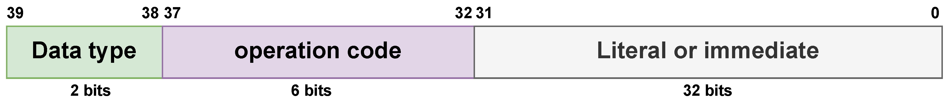
Figure 2.
Proposed multicycle microprocessor based on Harvard microarchitecture.
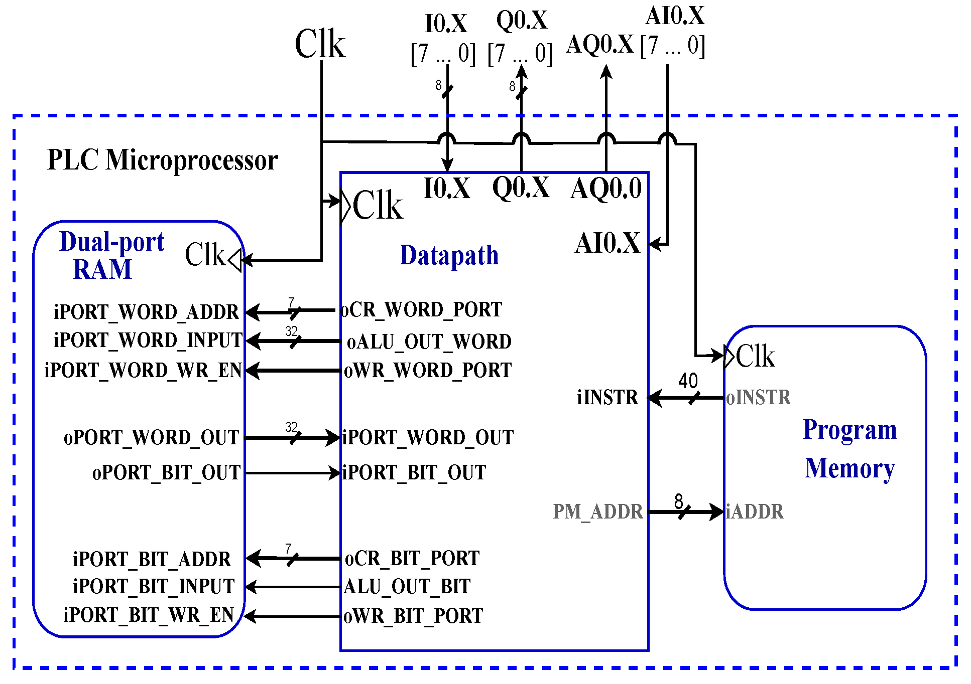
Figure 3.
The general microarchitecture and its control unit.
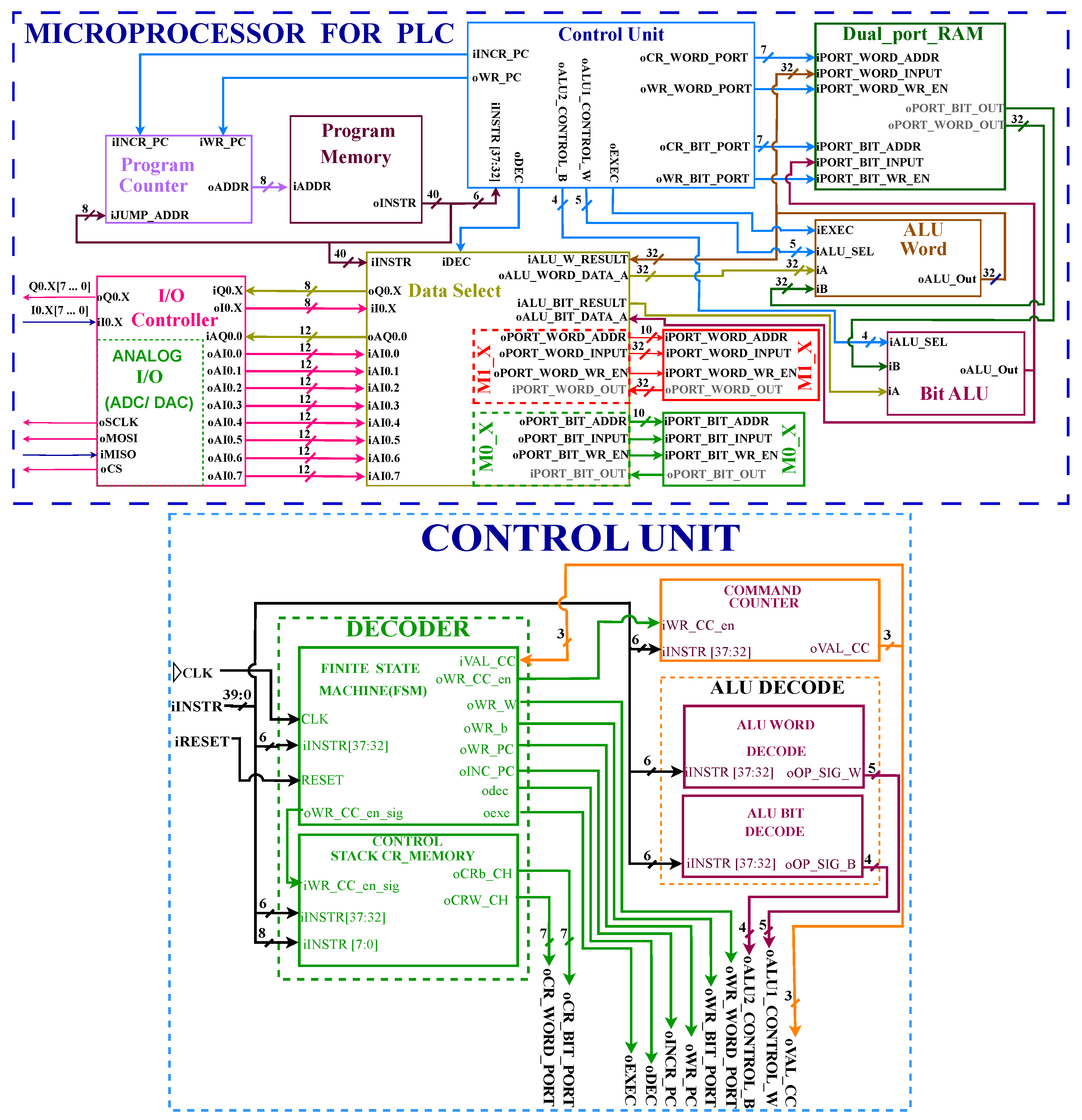
Figure 4.
State machine stages in the execution of instructions.
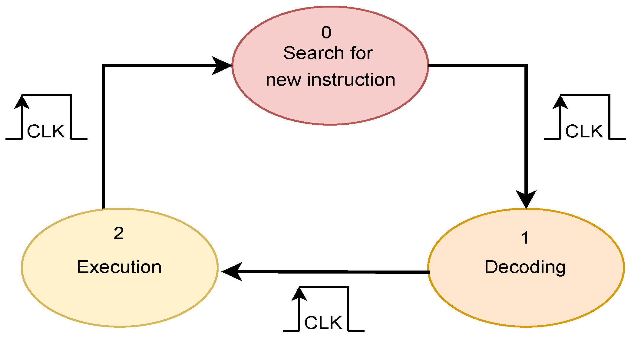
Figure 5.
(a) the Intel-Altera RTL, (b) the data path RTL, (c) the control unit RTL, (d) the FPU RTL, and (b) the FPGA resource utilization report for the proposed microprocessor designed for PLC applications.
Figure 5.
(a) the Intel-Altera RTL, (b) the data path RTL, (c) the control unit RTL, (d) the FPU RTL, and (b) the FPGA resource utilization report for the proposed microprocessor designed for PLC applications.
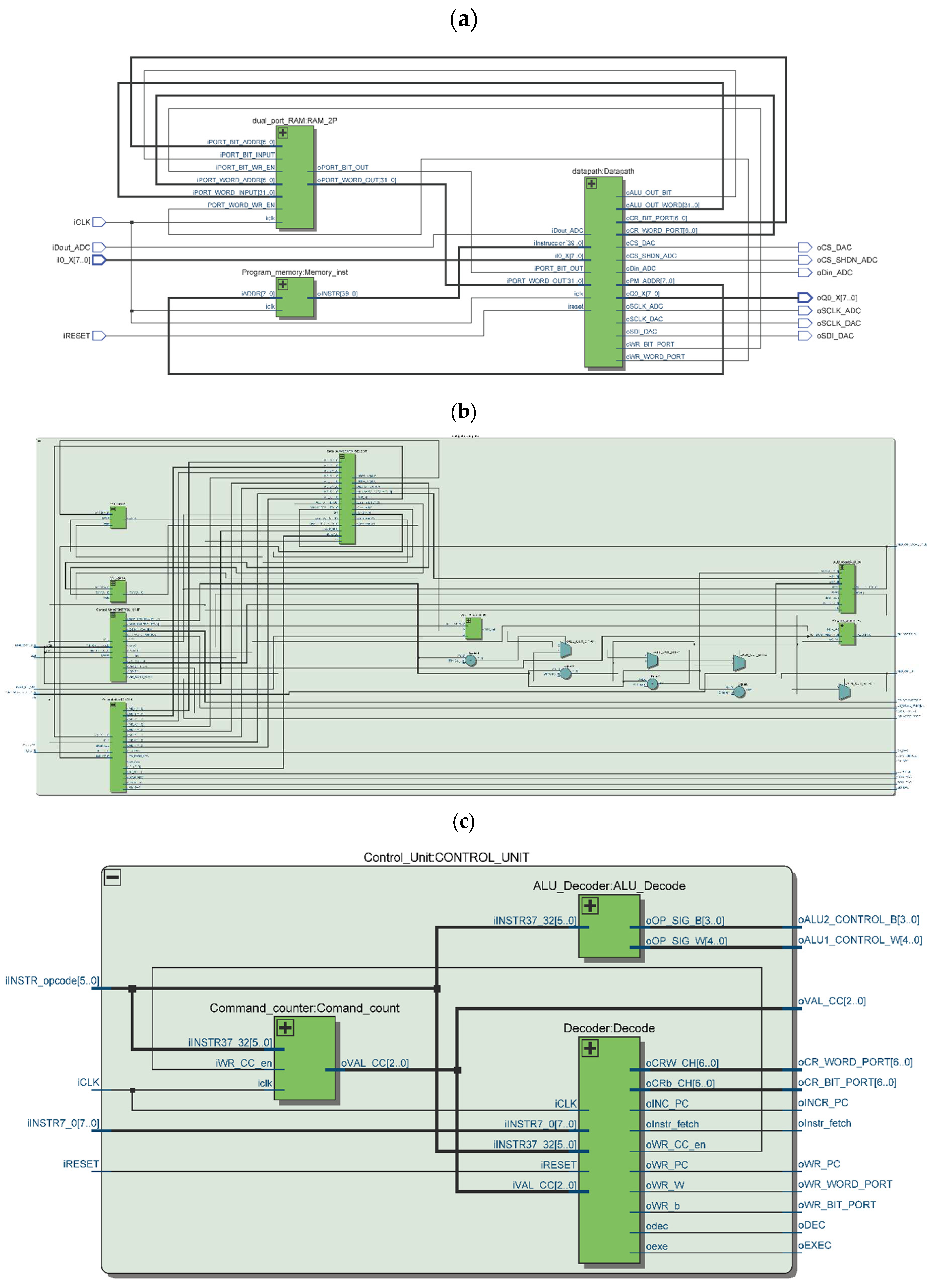
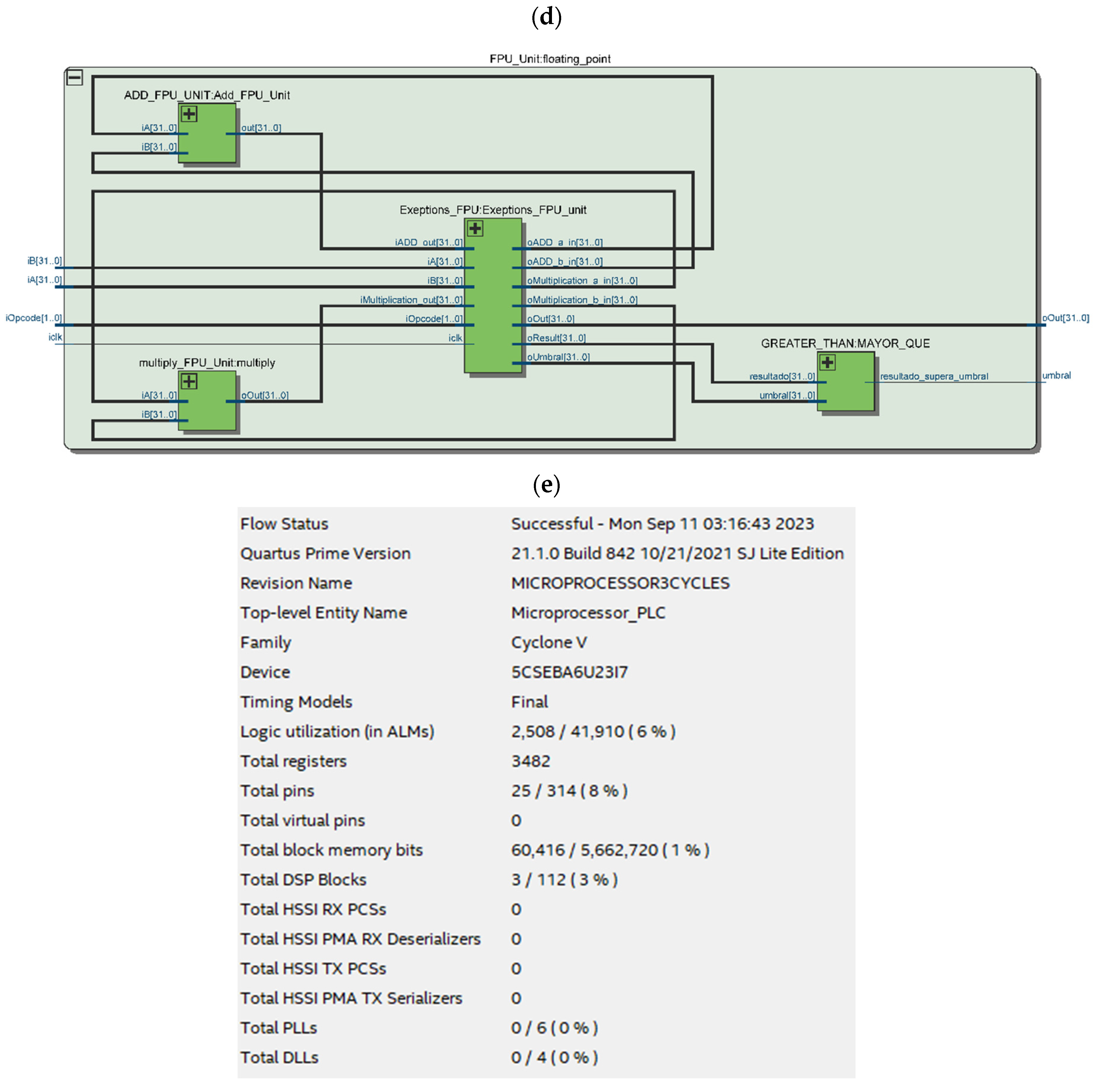
Figure 6.
System implemented for the first case study.
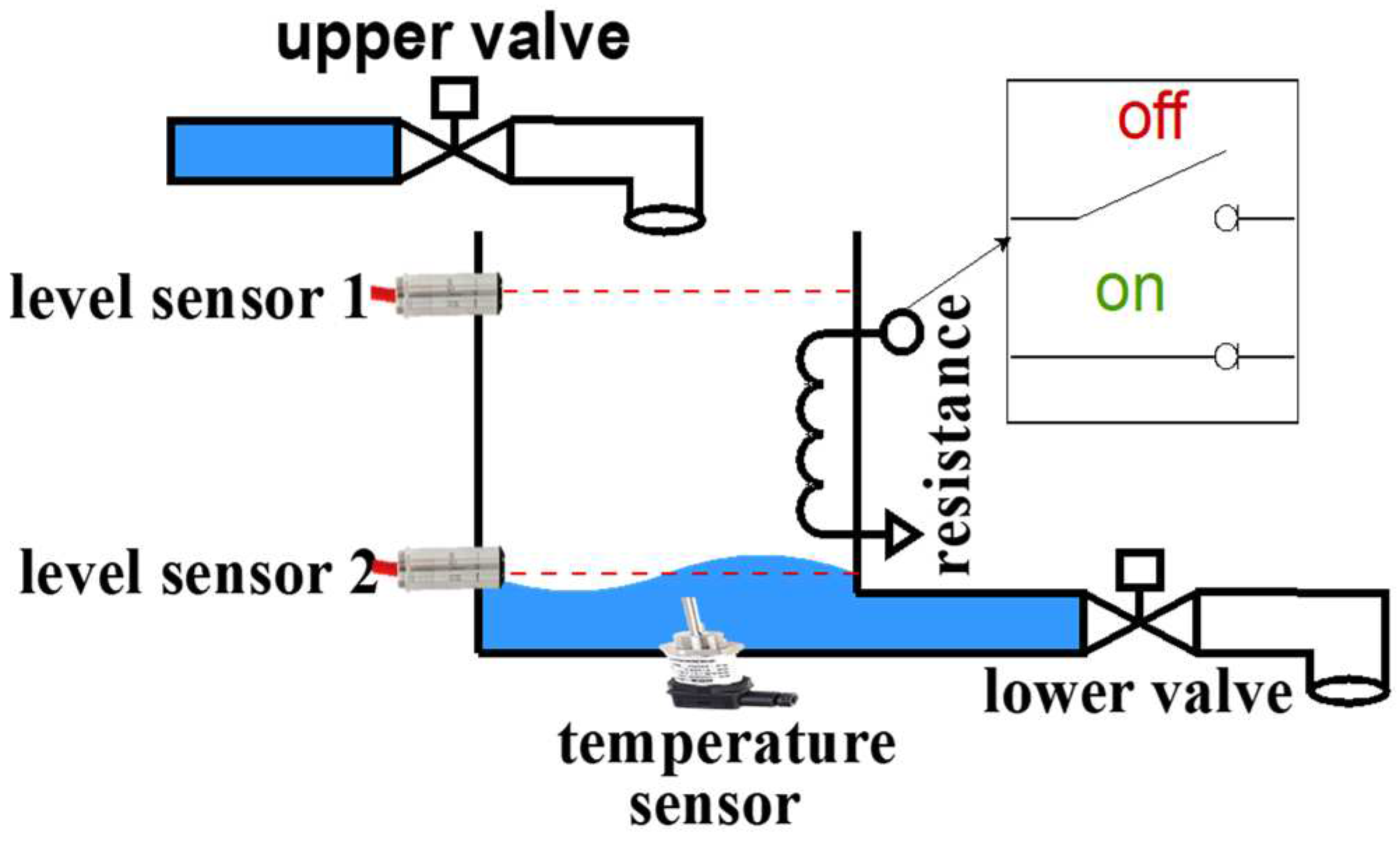
Figure 7.
System implemented for the first case study.
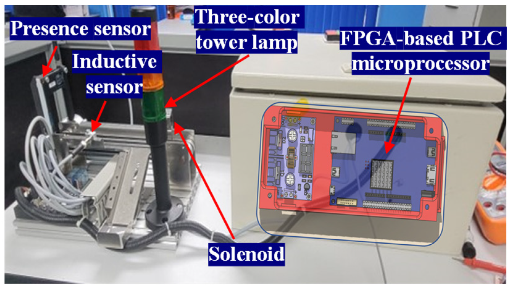
Figure 8.
(a) Reduced diagram of water heater tank filling system simulation, system startup, (b) Reduced simulation diagram of water heater tank filling system, tank filling valve opening, and (c) Reduced simulation diagram of water heater tank filling system, tank filling valve opening.
Figure 8.
(a) Reduced diagram of water heater tank filling system simulation, system startup, (b) Reduced simulation diagram of water heater tank filling system, tank filling valve opening, and (c) Reduced simulation diagram of water heater tank filling system, tank filling valve opening.
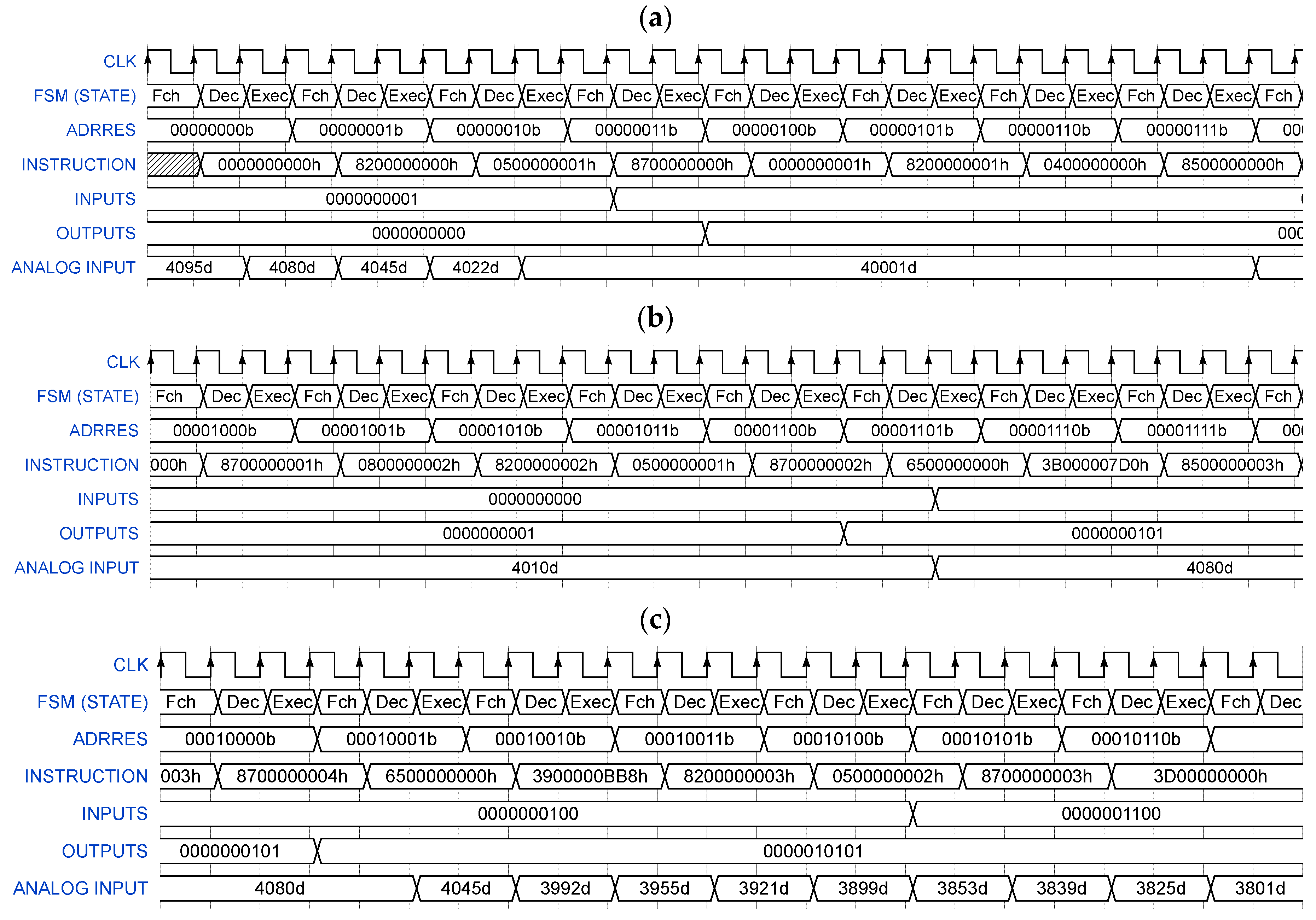
Figure 10.
Description of the motor interlock in LD.06.
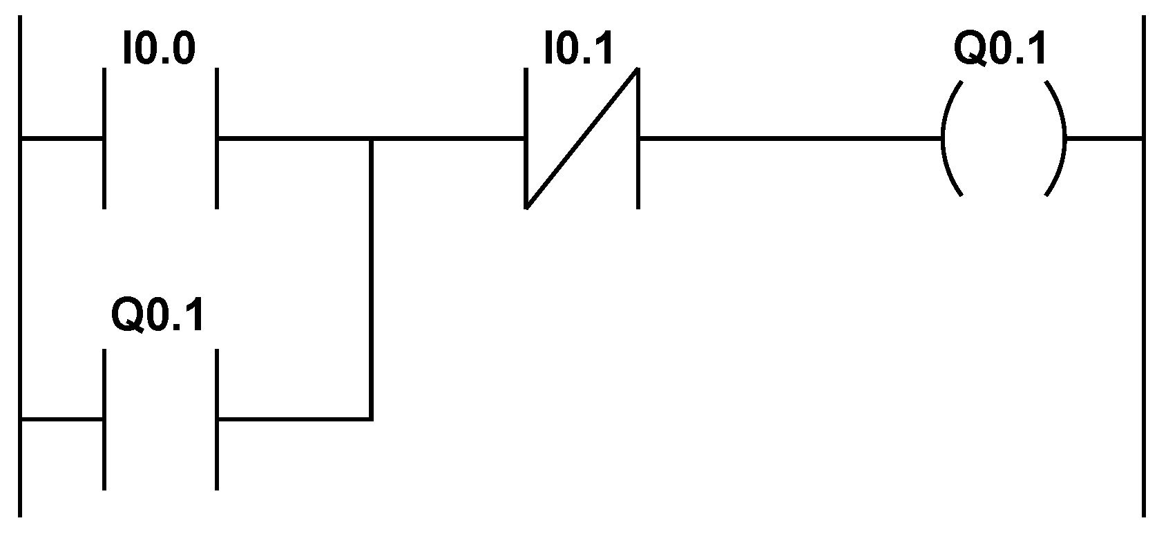
Figure 11.
Reduced simulation diagram of the motor interlock.
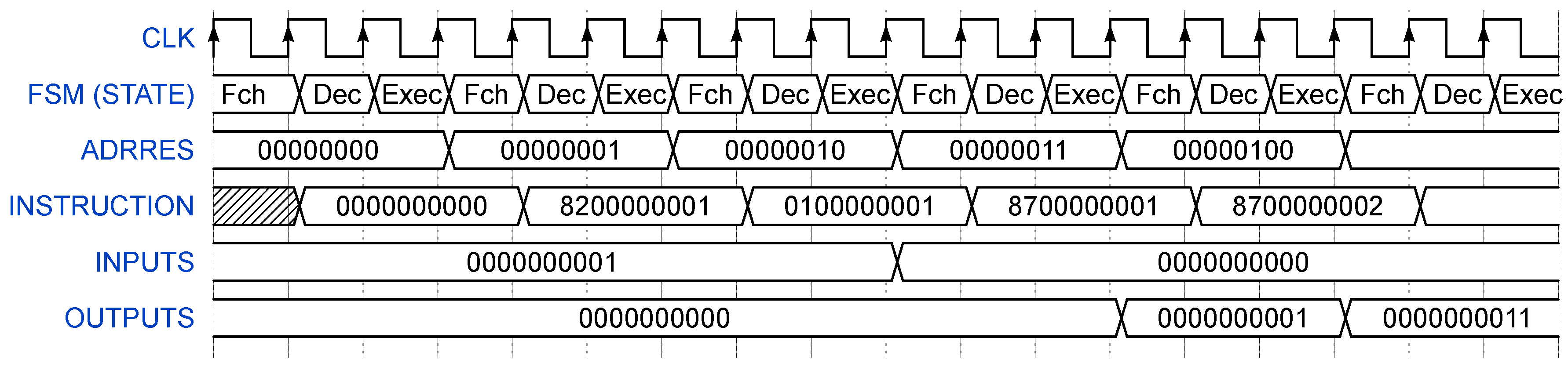

Table 1.
Typical classification in the proposed microprocessor.
| Description |
|---|
| Bitwise operations for a bit/double data |
| Rotate and Shift instructions |
| Floating-point Operations |
| Arithmetical Operations |
| Unconditional JUMP instruction |
Table 3.
Functions Of The 2P-RAM I/O Ports.
| Instruction | Description of the instruction |
|---|---|
| iPORT_WORD_ADDR | Sets the address of the selected register |
| iPORT_WORD_INPUT | Inserts the 32-bit data into memory |
| iPORT_WORD_WR_EN | Enables writing to memory |
| oPORT_WORD_OUT | The output port of the data obtained in RAM. |
| iPORT_BIT_ADDR | Sets the address of the selected register |
| iPORT_BIT_INPUT | Inserts the bit data into memory |
| iPORT_BIT_WR_EN | Enables writing to memory |
| oPORT_BIT_OUT | The output port of the data obtained in RAM. |
Table 4.
Configuration of operations implemented in the word ALU.
| Op. code | Description of the operation | Operation performed |
|---|---|---|
| 5’b00000 | The sum of two operands | oALU_RES = iA + iB |
| 5’b00001 | Subtraction of two operands | oALU_RES = iA - iB |
| 5’b00010 | Multiplication of two operands | oALU_RES = iA * iB |
| 5’b00011 | Division of two operands | oALU_RES = iA/iB |
| 5’b00100 | Logical shift to the left | oALU_RES = iB << iN |
| 5’b00101 | Logical shift to the right | oALU_RES = iB >> iN |
| 5’b00110 | Rotate left | oALU_RES = ROL(iB) |
| 5’b00111 | Rotate to the right | oALU_RES = ROR(iB) |
| 5’b01000 | Logical AND operation | oALU_RES = iA & iB |
| 5’b01001 | Logical OR operation | oALU_RES = iA | iB |
| 5’b01010 | Logical XOR operation | oALU_RES = iA ^ iB |
| 5’b01011 | Logical NOR operation | oALU_RES = ~(iA | iB) |
| 5’b01100 | Logical NAND operation | oALU_RES = ~(iA & iB) |
| 5’b01101 | Logical XNOR operation | oALU_RES = ~(iA ^ iB) |
| 5’b01110 | Comparison greater than | oALU_RES = (iB>iA)? |
| 5’b01111 | Comparison equalization | oALU_RES = (iB==iA)? |
| 5’b10000 | Floating point sum | oALU_RES = iA + iB |
| 5’b10001 | Floating point subtraction | oALU_RES = iA - iB |
| 5’b10010 | Floating point multiplication | oALU_RES = iA * iB |
| 5’b10011 | Floating point division | oALU_RES = iA/iB |
| 5’b10100 | Load data from the current result | oALU_RES = iB |
| 5’b10101 | Load data from data selector | oALU_RESULT = iA |
| 5’b10110 | Comparison less than | oALU_RES = (iB<iA)? |
Table 5.
Configuration of operations implemented in the bit ALU.
| Op. code | Description of the operation | Operation performed |
|---|---|---|
| 4’b0000 | Load data from data selector | oALU_RES = iA |
| 4’b0001 | Logical AND operation | oALU_RES = iA & iB |
| 4’b0010 | Logical OR operation | oALU_RES = iA | iB |
| 4’b0011 | Logical XOR operation | oALU_RES = iA ^ iB |
| 4’b0100 | Logical ORN operation | oALU_RES = ~iA | iB |
| 4’b0101 | Logical ANDN operation | oALU_RES = ~iA & iB |
| 4’b0110 | Logical XNOR operation | oALU_RES = iA ~^ iB |
| 4’b0111 | Load data from the current result | oALU_RES = iB |
| 4’b1000 | Load bit denied | oALU_RES = ~iA |
Table 6.
Description of the data selector ports.
| Data selector ports | Description |
|---|---|
| iINSTR | 40-bit instruction input port |
| iDEC | Indicator signal input port for decoding stage |
| oALU_WORD_DATA_A | Output port for the word ALU |
| iALU_W_RESULT | Word ALU Result Input Port |
| oALU_BIT_DATA_A | The output port of the first operand for the bit ALU |
| iALU_BIT_RESULT | Bit ALU result input port |
| M0_X | M0X memory bank |
| M1_X | M1X memory bank |
| oQ0.X | Communication ports for the 8 digital outputs |
| iI0.X | Communication ports for the 8 digital inputs |
| iAI0.X | Communication ports for the 8 analog inputs |
| oAQ0.0 | Communication ports for analog output |
Table 7.
Coding of the data type in word instructions.
| Op. code | Data type |
|---|---|
| 2’b00 | Literal or immediate |
| 2’b01 | Analog inputs |
| 2’b10 | Analog outputs |
| 2’b11 | Memory block words |
Table 8.
Coding of the data type in bits instructions.
| Op. code | Data type |
|---|---|
| 2’b00 | Digital inputs |
| 2’b01 | Memory block bits |
| 2’b10 | Digital outputs |
| 2’b11 | ----------- |
Table 9.
Description of the data selector ports.
| I/O controller ports | Description |
|---|---|
| oQ0.X | Port of the 8 digital outputs |
| iI0.X | Port of the 8 digital inputs |
| iAQ0.0 | Data input port for analog output |
| oAI0.0 … 7 | Port of the 8 analog outputs |
| oSCLK | SPI communication clock output port |
| oMOSI | Output port for master-slave SPI communication |
| iMISO | Input port for master-slave SPI communication |
| oCS | SPI communication selects the chip output port |
Table 10.
Code used to implement the case study.
| Instruction | Operation | Operator |
|---|---|---|
| 40′h0000000000 | LD | I0.0 |
| 40′h8200000000 | OR | Q0.0 |
| 40′h0500000001 | ANDN | I0.1 |
| 40′h8700000000 | ST | Q0.0 |
| 40′h0000000001 | LD | I0.1 |
| 40′h8200000001 | OR | Q0.1 |
| 40′h0400000000 | ORN | I0.0 |
| 40′h8500000000 | ANDN | Q0.0 |
| 40′h8700000001 | ST | Q0.1 |
| 40′h0800000002 | LD_NEG | I0.2 |
| 40′h8200000002 | OR | Q0.2 |
| 40′h0500000001 | ANDN | I0.3 |
| 40′h8700000002 | ST | Q0.2 |
| 40′h6500000000 | LD | AI0.0 |
| 40′h3B000007D0 | LT | 3434 |
| 40′h8500000003 | ANDN | Q0.3 |
| 40′h8700000004 | ST | Q0.4 |
| 40′h6500000000 | LD | AI0.0 |
| 40′h3900000C6F | GT | 3183 |
| 40′h8200000003 | OR | Q0.3 |
| 40′h0500000002 | ANDN | I0.2 |
| 40′h8700000003 | ST | Q0.3 |
| 40′h3D00000000 | JMP | 000 |
Table 11.
Pt-100 sensor resistance, voltage, and current in the 0 °C–150 °C range using 12-bit format.
Table 11.
Pt-100 sensor resistance, voltage, and current in the 0 °C–150 °C range using 12-bit format.
| ] | R [PT100] [Ohm] | [PT100] [V] | [PT100] [mA] | Digit 12bit format |
|---|---|---|---|---|
| 0 | 100 | 2.50 | 25 | 4095 |
| 50 | 119.40 | 2.28 | 19.09 | 3733 |
| 100 | 138.51 | 2.10 | 15.13 | 3434 |
| 150 | 157.33 | 1.94 | 12.35 | 3183 |
Table 12.
Code used to implement the case study.
| Instruction | Operation | Operator |
|---|---|---|
| 40′h0000000000 | LD | I0.0 |
| 40′h8200000001 | OR | Q0.1 |
| 40′h0100000001 | AND | I0.1 |
| 40′h8700000001 | ST | Q0.1 |
| 40′h8700000002 | ST | Q0.2 |
| 40′h0000000002 | LD | I0.2 |
| 40′h8200000000 | OR | Q0.0 |
| 40′h0500000003 | ANDN | I0.3 |
| 40′h8700000000 | ST | Q0.0 |
| 40′h0000000003 | LD | I0.3 |
| 40′h8700000003 | ST | Q0.3 |
| 40′h0000000001 | LD | I0.1 |
| 40′h8200000001 | OR | Q0.4 |
| 40′h8500000001 | ANDN | Q0.1 |
| 40′h8700000004 | ST | Q0.4 |
| 40′h3D00000000 | JMP | 000 |
Table 13.
Configuration of operations implemented in the word ALU.
| Instruction | Description of the instruction | S. S7-312 [23] |
S. S7-319 [23] |
Ref. [20] | This work |
|---|---|---|---|---|---|
| CPU Time |
CPU Time |
||||
| LD_W | Load word | - | - | - | 60 ns |
| ST_W | Stores word | - | - | - | 60 ns |
| ADD_I | Sum of integers | 220 ns | 10 ns | 80 ns | 60 ns |
| SUB_I | Subtraction of integers | 220 ns | 10 ns | 80 ns | 60 ns |
| MUL_I | Word multiplication | 210 ns | 8 ns | 80 ns | 60 ns |
| DIV_I | Word division | 900 ns | 6000 ns | 800 ns | 60 ns |
| ADD_R | FPU sum | 1100 ns | 40 ns | 160 ns | 60 ns |
| SUB_R | Floating point subtraction | 1100 ns | 40 ns | 160 ns | 60 ns |
| MUL_R | Floating point multiplication | 1110 ns | 40 ns | 80 ns | 60 ns |
| SL | Shift left | 460 ns | 19 ns | 80 ns | 60 ns |
| SR | Shift right | 460 ns | 19 ns | 80 ns | 60 ns |
| RL | Rot. Left | 450 ns | 19 ns | 80 ns | 60 ns |
| RR | Rot. Right | 450 ns | 19 ns | 80 ns | 60 ns |
| AND_W | btwn words | 280 ns | 14 ns | - | 60 ns |
| OR_W | btwn words | 280 ns | 14 ns | - | 60 ns |
| XOR_W | btwn words | 280 ns | 14 ns | - | 60 ns |
| NOR_W | btwn words | - | - | - | 60 ns |
| NAND_W | btwn words | 900 ns | 6000 ns | - | 60 ns |
| XNOR_W | btwn words | - | - | - | 60 ns |
| GT | Greater than | 430 ns | 23 ns | 80 ns | 60 ns |
| ET | As well as | 430 ns | 23 ns | 80 ns | 60 ns |
| LT | Less than | - | - | - | 60 ns |
| LD | Load bit | - | - | - | 60 ns |
| AND | btwn bits | 280 ns | 14 ns | 80 ns | 60 ns |
| OR | btwn bits | 280 ns | 14 ns | 80 ns | 60 ns |
| XOR | btwn bits | 280 ns | 14 ns | - | 60 ns |
| ORN | btwn bits | - | - | 80 ns | 60 ns |
| ANDN | btwn bits | - | - | - | 60 ns |
| XNOR | btwn bits | - | - | - | 60 ns |
| ST | Stores bit | - | - | - | 60 ns |
| LD_NEG | Load bit denied | - | - | - | 60 ns |
| JMP | Line break | - | - | - | s |
Disclaimer/Publisher’s Note: The statements, opinions and data contained in all publications are solely those of the individual author(s) and contributor(s) and not of MDPI and/or the editor(s). MDPI and/or the editor(s) disclaim responsibility for any injury to people or property resulting from any ideas, methods, instructions or products referred to in the content. |
© 2023 by the authors. Licensee MDPI, Basel, Switzerland. This article is an open access article distributed under the terms and conditions of the Creative Commons Attribution (CC BY) license (http://creativecommons.org/licenses/by/4.0/).
Copyright: This open access article is published under a Creative Commons CC BY 4.0 license, which permit the free download, distribution, and reuse, provided that the author and preprint are cited in any reuse.


