1. Introduction
The swift advancement of electronic technology has given rise to the necessity for low-power and high-performance circuit design [
1,
2,
3,
4]. In this context, fundamental building blocks of any chip, such as operational amplifiers, low-dropout regulators (LDOs), and bandgap references, have become increasingly important. Maintaining circuit stability under diverse operating conditions thus becomes critical. The PSRR serves as a key metric for assessing a circuit’s ability to suppress power supply noise, directly impacting signal integrity and system stability. In the realm of high-precision medical devices [
5], enhancing the PSRR augments measurement precision and diagnostic reliability. In high-speed communication systems, it attenuates noise interference during data transmission. And in portable devices, it prolongs battery life and enhances immunity to interference.
Conventional PSRR calculation methods rely predominantly on simplified analyses of system poles and zeros, often using low-frequency equivalent circuit models [
6,
7,
8]. However, as circuits operate at higher frequencies, parasitic capacitance, inductance, and other high-frequency effects introduce significant deviations between calculated and actual performance. This discrepancy becomes even more pronounced in radio frequency (RF) and high-speed communication circuits, where complex interactions between power supply noise and parasitic parameters exacerbate the issue. Moreover, existing methods lack a unified theoretical framework and standardized calculation process, forcing designers to invest substantial time in theoretical derivation and experimental validation when addressing novel circuit architectures. Such constraints hinder design efficiency and innovation.
Researchers have proposed various circuit-level techniques to improve PSRR, but each comes with shortcomings that underscore the need for a general modeling approach. For instance, Kim introduced an NMOS LDO regulator with an intrinsic gain-tracking ripple cancellation technique to achieve high PSRR [
9]. Similarly, Zhang employed a chopper stabilization scheme in a Class-D audio amplifier to maintain a high PSRR across the entire audio band [
10]. While effective, such solutions are tailored to specific applications (voltage regulators or amplifiers) and do not provide a broadly applicable theory for PSRR prediction. In addition, many designs still struggle to sustain high PSRR at elevated frequencies. For example, an output-capacitor-less LDO designed for ultra-low voltage achieved only about 30 dB PSRR at 10 kHz, illustrating how traditional design techniques can fall short in high-frequency or low-headroom scenarios [
11]. These recent works demonstrate the importance of PSRR optimization but also highlight the inadequacy of existing methods to generalize across different circuits and operating conditions. A more universal modeling approach is needed to predict and optimize PSRR from DC up to the mid-frequency range in a systematic, time-efficient manner.
To address these challenges, we propose a black-box modeling approach for PSRR prediction in multi-stage op-amps. The core idea is to collapse the multi-stage amplifier into a simplified equivalent model using Thevenin’s theorem, treating the first amplification stage as an abstracted black box. By deriving the Thevenin-equivalent output of the first stage and reintegrating it into the overall circuit, the PSRR calculation is greatly simplified without sacrificing accuracy. This approach yields an analytical yet intuitive understanding of how each stage contributes to the overall PSRR, and it naturally incorporates important design parameters such as pole-zero locations and gain-bandwidth limits. Compared to brute-force simulation or complex small-signal models, the black-box method significantly reduces the mathematical effort required to evaluate PSRR, making it accessible for early-stage design and optimization.
In addition, we introduce a new metric called the Power-Supply Rejection Gain-Bandwidth (PGB) product to characterize high-frequency PSRR behavior. By analogy to the op-amp gain-bandwidth product, the PGB is defined as the product of the DC PSRR value and the frequency of the dominant PSRR zero. This metric captures the fundamental trade-off between low-frequency suppression and the frequency range over which that suppression is effective. A higher PGB indicates that the PSRR remains strong over a broader bandwidth, whereas a lower PGB means the PSRR begins to deteriorate at a lower frequency. Using the PGB metric, one can more intuitively analyze the design trade-offs between PSRR and other performance parameters (such as stability or bandwidth) within the target frequency range. An important advantage of the PGB-based evaluation is that it avoids the need for tedious high-frequency small-signal modeling (e.g. large matrix S-parameter analysis). Instead, the PSRR and first-pole characteristics are extracted directly to yield an efficient, first-order prediction of PSRR performance across frequency. The proposed method is applicable from DC up to the op-amp’s unity-gain bandwidth (UGB). Notably, it provides a unified explanation for why different circuit architectures with the same low-frequency PSRR and pole configuration can exhibit divergent PSRR roll-off behaviors as they approach the UGB. For example, an LDO regulator and a two-stage op-amp (each optimized for similar DC PSRR) might have different PSRR values at mid-frequency (near their UGB), due to differences in internal gain distribution and zero/pole placement.
We validate the proposed method by analyzing typical circuit structures. The rest of this paper is organized as follows. Section II reviews the traditional PSRR calculation methods and introduces the theoretical basis of our method and details the PSRR calculation process and zero-pole characteristics of different circuits. Section III verifies the accuracy of PSRR calculation through the design and simulation of complex circuits and confirms the feasibility of optimizing PSRR through PGB calculation analysis. Finally, Section IV summarizes the advantages of the proposed method and outlines the direction of future research.
2. Materials and Methods
2.1. Related Work
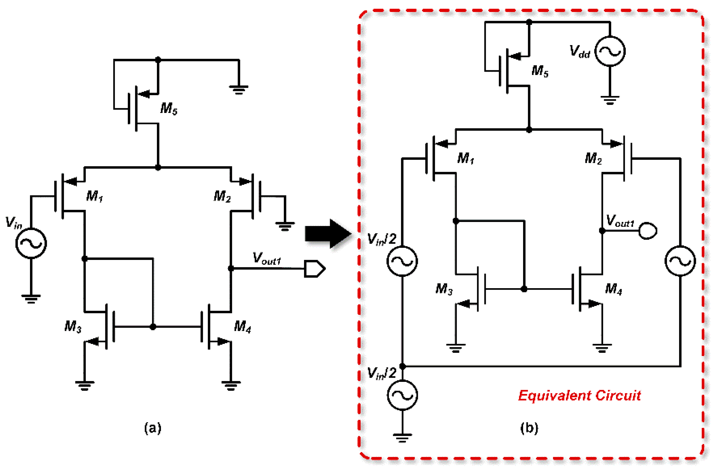
We leverage Allen's interpretation of PSRR [
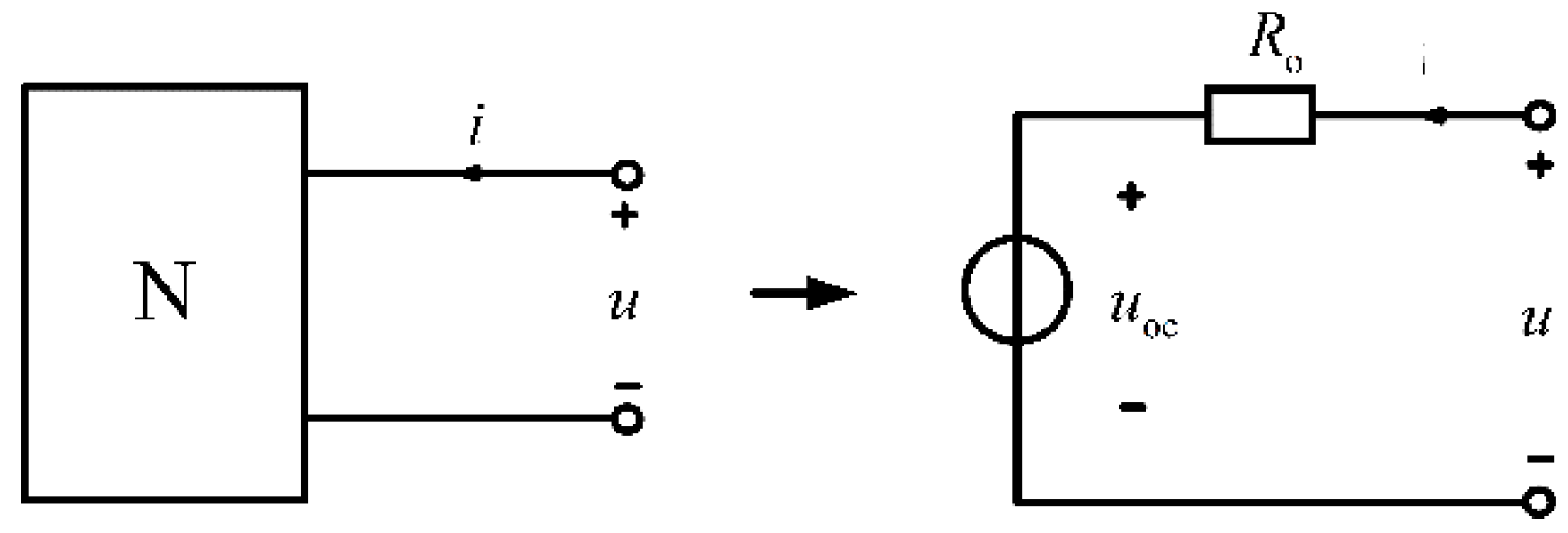
7] and develop a "black-box" model that simplifies the intricate circuitry. This model is particularly applicable to Thevenin Equivalent Circuit Analysis, where the Thevenin theorem simplifies linear resistor networks with independent sources into a single voltage source in series with a resistance. Specifically, for any single-port network N, the port can be represented equivalently by a voltage source —whose value corresponds to the open-circuit voltage (u
oc)—in series with a resistance R
o, which is the equivalent resistance observed at the port when all independent sources are deactivated.
Figure 1.
Thevenin equivalent circuit.
Figure 1.
Thevenin equivalent circuit.
2.2. Proposed Methodology
In this section, we employ the proposed black-box theory to analyze the PSRR of various operational amplifiers.
2.2.1. PSRR Calculation for P-Input Two-Stage Op-Amps
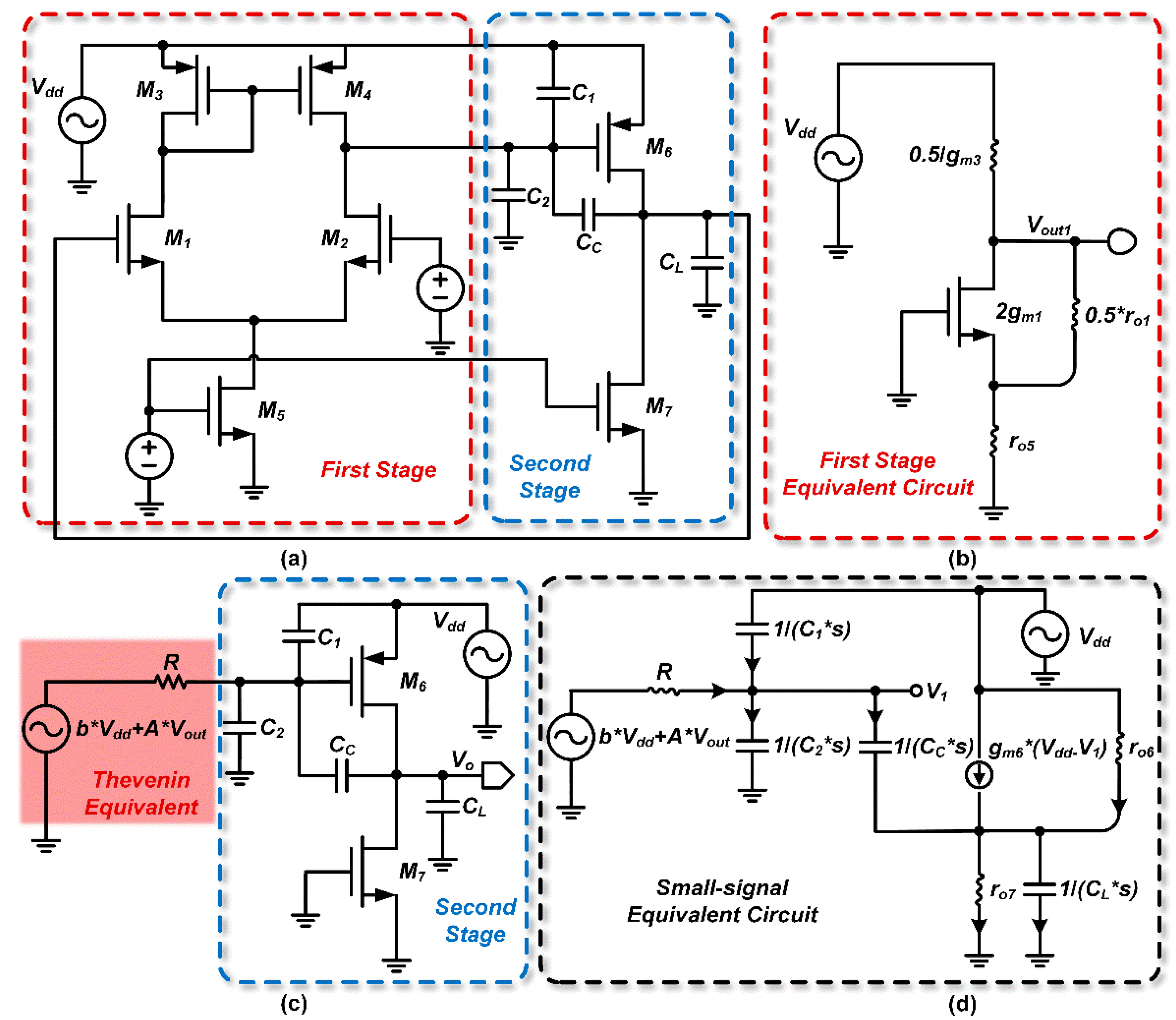
Figure 2.
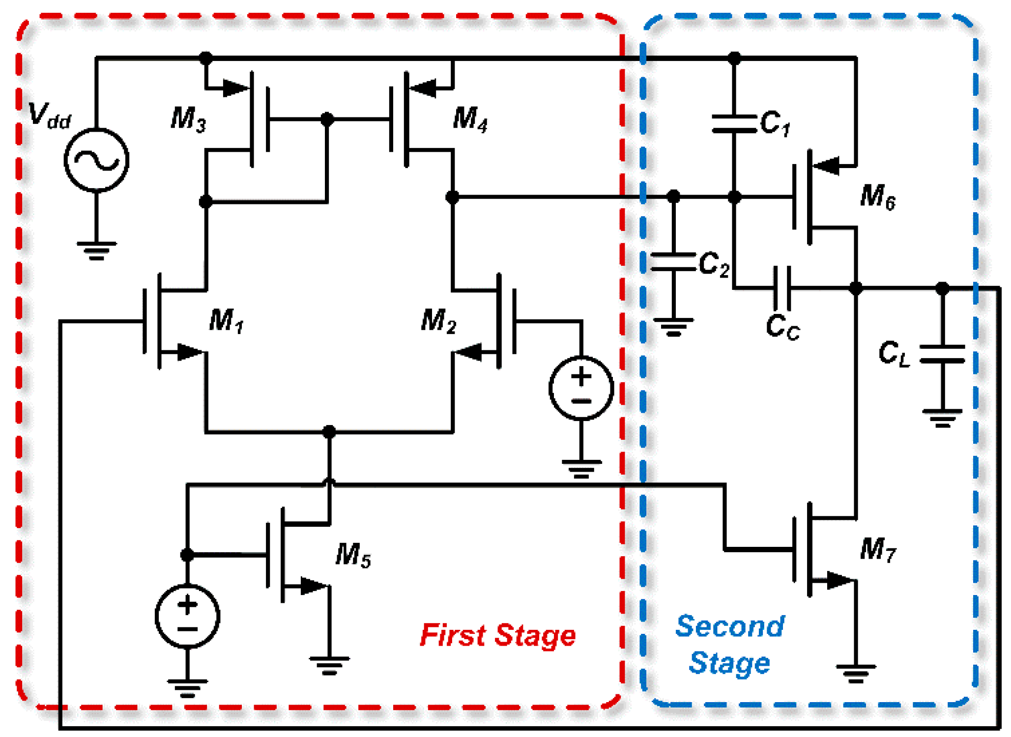
Typical structure of a P-input two-stage op-amp.
Figure 2.
Typical structure of a P-input two-stage op-amp.
In this op-amp, the input stage usually consists of two P-type MOSFETs (M1 and M2) that receive the input signal and provide initial amplification. Transistors M3 and M4 act as load devices and work in conjunction with M1 and M2 to enhance the gain of the input stage. Current mirrors comprising M5 and M7 supply a stable bias current to the input stage while ensuring that the currents in M1 and M2 are matched. In the output stage, transistor M6 further amplifies the signal from the input stage and provides sufficient drive capability for the load.
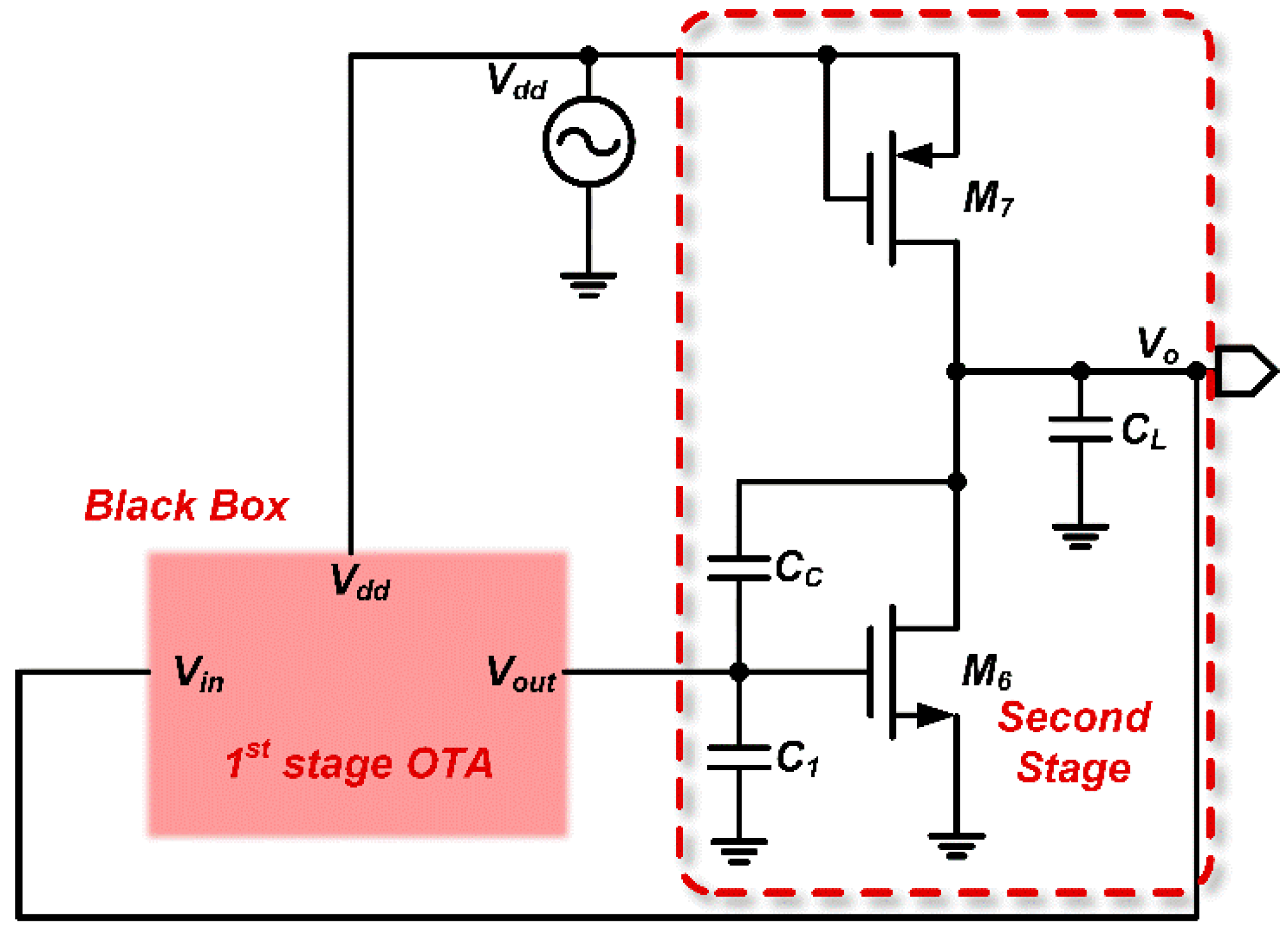
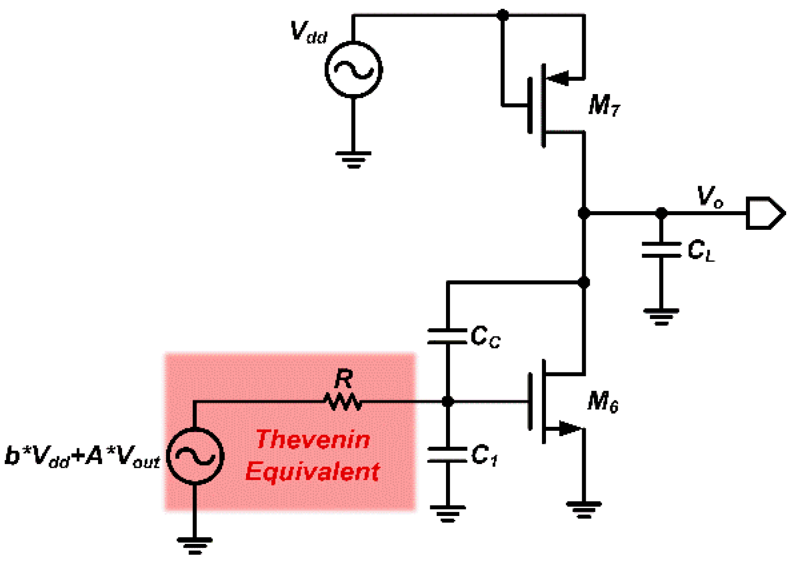
To simplify the calculation, we treat the first stage of the op-amp as a “black box” with input terminals which denoted as
and an output terminal which denoted as
. This is illustrated in
Figure 3.
Figure 3.
Two-stage op-amp circuit after “black-box” abstraction.
Figure 3.
Two-stage op-amp circuit after “black-box” abstraction.
The processing of the first stage is performed in several steps:
- a)
Evaluating the Impact of on the Thevenin Equivalent Output Voltage of the First Stage
Figure 4.
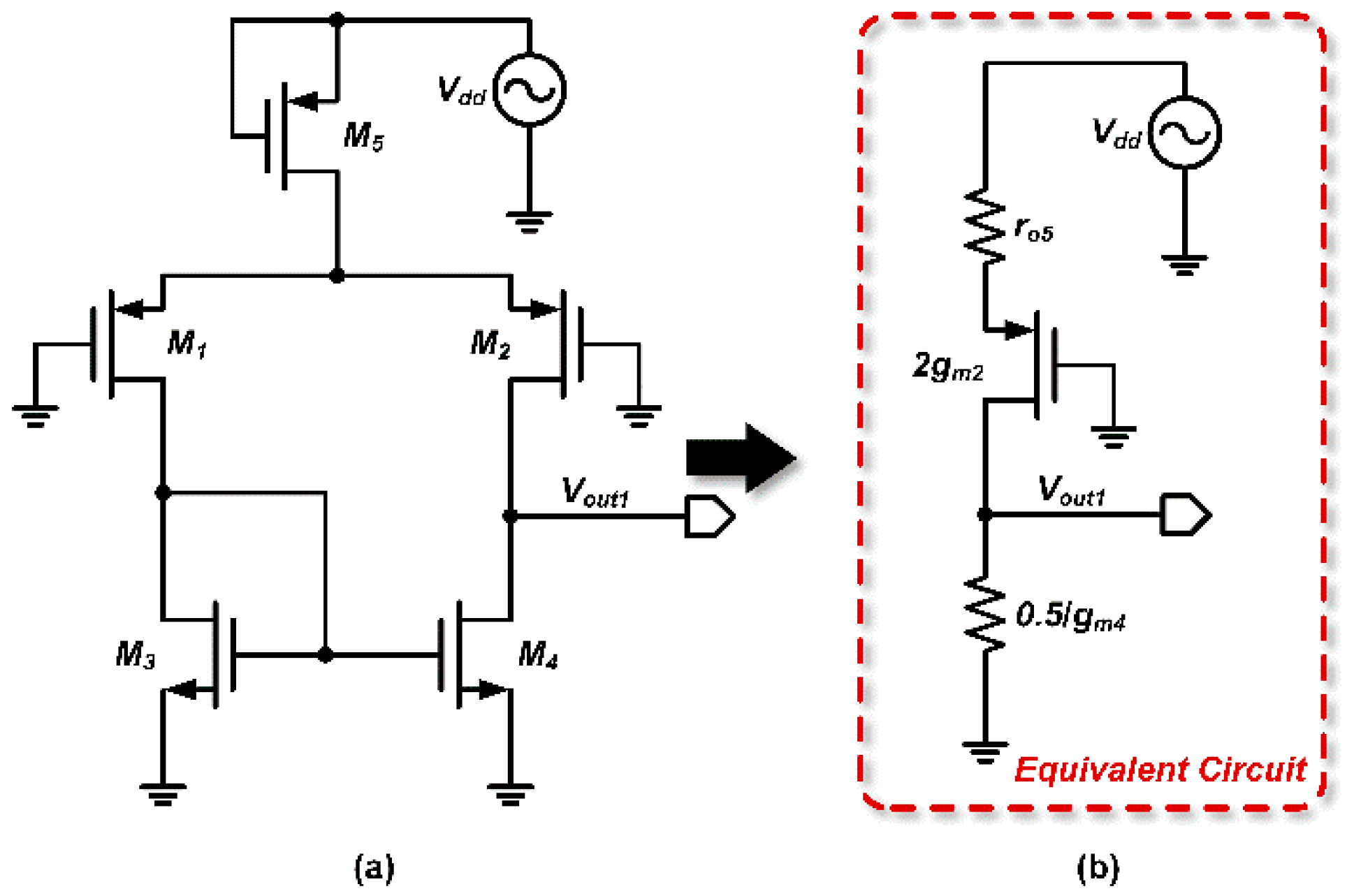
Thevenin equivalent circuit for the first stage of the op-amp.
Figure 4.
Thevenin equivalent circuit for the first stage of the op-amp.
The first stage is viewed as an independent module. Based on the Thevenin theorem, the equivalent voltage generated by
is given by
.
- b)
Evaluating the Impact of on the Thevenin Equivalent Output Voltage of the First Stage
Figure 5.
Thevenin equivalent output voltage of the first stage.
Figure 5.
Thevenin equivalent output voltage of the first stage.
For a differential input
, the corresponding Thevenin equivalent output voltage is:
Likewise, for a common-mode input
, the corresponding Thevenin equivalent output voltage is:
The common-mode output voltage is relatively small and can be combined with the differential output voltage. Therefore, in the subsequent calculations, the common-mode contribution is typically neglected.
- c)
Constructing the Thevenin Equivalent Circuit
Using the superposition theorem, the first stage is further simplified to a structure consisting of a voltage source and a resistor, as shown in the lower left area of
Figure 6, where
represents the output resistance of the first stage.
- d)
Deriving the PSRR Transfer Function
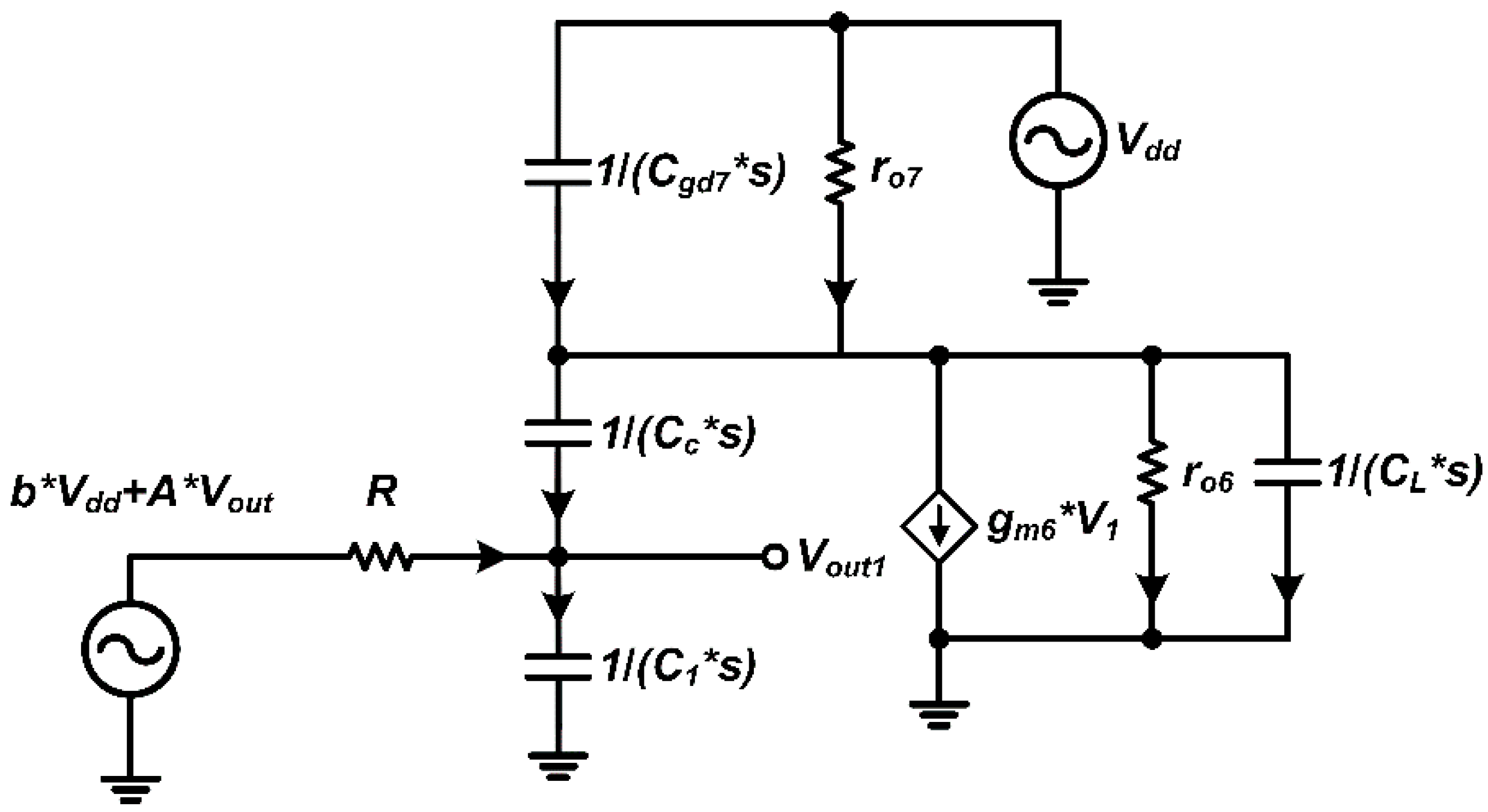
The equivalent circuit for the two-stage op-amp is shown in
Figure 7. Considering the gate-drain capacitance C
gd of M
7, we use small-signal analysis to write the node current equations and thereby solve for the PSRR transfer function.
Moreover, in the PSRR transfer function derived from the black-box model, two primary zeros emerge, denoted Z1 and Z2. The first zero, Z1, corresponds to the frequency at which supply-induced noise contributions from the first and second amplifier stages cancel each other, resulting in a null (zero) in the PSRR response. The second zero, Z2, occurs at a higher frequency and typically arises from a secondary coupling mechanism or parasitic feedback path within the op-amp. For clarity in analysis, we assume Z1 lies at a lower frequency than Z2. This assumption isolates the low-frequency behavior dominated by Z1 and aligns with the typical frequency ordering in multi-stage analog circuits. Similarly, when examining the pole locations, we will assume a dominant low-frequency pole (p1 < p2) to maintain consistency in the frequency-domain analysis. With these definitions and assumptions in place, we now proceed to derive the DC PSRR value and identify the corresponding zero and pole positions. It should be noted that in common multi-stage amplifiers, the two zeros caused by the first-stage output and third-stage feedback equivalence usually satisfy Z1 < Z2.
First, we write the node current equation at node
:
Similarly, writing the node current equation at node
:
In the derivation above, it is assumed that
, due to matching requirements. if we set
and
,we obtain that
,
, and:
Next, we derive the DC PSRR value as well as the positions of the zero and pole:
Assuming
Z1 <<
Z2,
Cgd7
<<
CC,
C1 <<
CC, and for
stability, we have
:
Further assuming
, leads to:
The location of is the closest to the origin relative to the first pole. Whether the DC PSRR value is positive or negative depends on the specific values of N and M When N is approximately twice that of M, the DC PSRR value becomes very high; however, the zero also shifts closer to the origin.
The PSRR is influenced by two signal paths within the op-amp. In the first path, the signal entering from reduces the output voltage at low frequencies; in the second path, the signal entering from has the opposite effect and increases the output voltage. For simplification, the drain of M5 is grounded, thereby neglecting the signal contribution from M5 and resulting in a positive DC PSRR gain. Under ideal bias current source conditions, if N is greater than twice that of M, the PSRR is negative; if N is less than twice that of M, the PSRR is positive. The location of the zero is also closely related to the ratio of these two parameters.
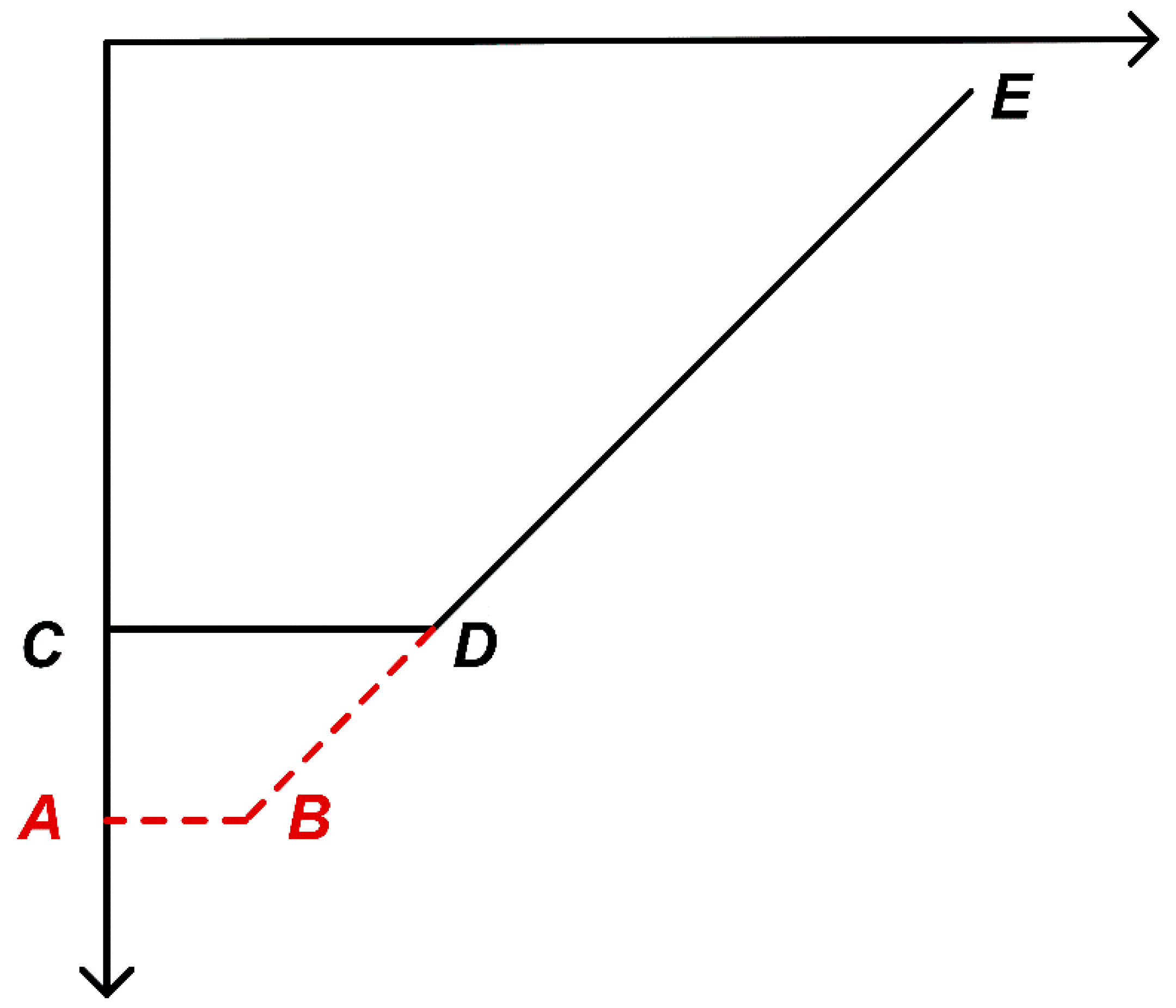
PGB (PSR Gain Bandwidth):
By approximating the PSRR curve as having a single zero, and drawing an analogy with the gain-bandwidth product in op-amps, we define PGB as the product of the zero frequency and the DC PSRR value:
Figure 8 illustrates a simplified PSRR curve (dominated by a single zero) to explain the PGB concept. The baseline curve CDE represents the original PSRR response: point C marks the DC PSRR value, and point D is the dominant zero’s frequency, beyond which the PSRR magnitude declines at approximately –20 dB/decade (segment D–E). If a design parameter is increased toward 2M (with other parameters fixed), the PSRR shifts to curve ABE. In this modified response, point A indicates a significantly higher DC PSRR and point B is the new dominant zero at a lower frequency (closer to the origin). This adjustment boosts the PSRR at DC and low frequencies (enhancing the low-frequency portion around point C, i.e., the “C
L” segment) but causes the –20 dB/dec roll-off to begin earlier (segment B–E), so the overall PGB remains essentially unchanged. In other words, raising the DC PSRR alone improves supply-noise rejection in the low-frequency region but does not extend the high-frequency response—an analog to the gain–bandwidth trade-off in amplifiers. Consequently, if the operating frequency lies in the original curve’s high-frequency region (segment D–E), this parameter change provides little improvement at that frequency.
Figure 8.
Impact of varying gm3. the frequency characteristics of PSRR.
Figure 8.
Impact of varying gm3. the frequency characteristics of PSRR.
This process bears some similarity to considerations of the loop bandwidth (GB) of the two-stage op-amp. Increasing a particular parameter directly enhances the DC PSRR value, which is beneficial for our analysis. Under stability constraints, reducing the parameter Cc shifts outward, thereby improving the frequency response; similarly, increasing shifts the BE line outward; increasing and directly optimizes the DC PSRR value; while increasing and raises the DC PSRR value but also moves closer to the origin, benefiting only the low-frequency response—the PGB remains unchanged, and hence the improvement for high frequencies is limited. However, since the bandwidth that the industry is concerned about is usually low-frequency, PGB can play a vital role in the design of specific field.
2.2.2. PSRR Calculation for N-Input Two-Stage Op-Amps
In this subsection, we adopt a similar analytical approach to study the PSRR of N-input two-stage op-amps and thereby demonstrate the portability of the new PSRR calculation theory.
Based on the analysis in Section A for a typical P-input two-stage op-amp, we consolidate the simplified flowchart for a common N-input two-stage op-amp into a single diagram, as shown in
Figure 9.
Figure 9.
Simplified flow chart of a common N-input two-stage op amp.
Figure 9.
Simplified flow chart of a common N-input two-stage op amp.
The following quantities are computed: the Thevenin equivalent voltage due to from the first stage, the Thevenin equivalent voltage due to , the PSRR, the DC PSRR value, the zero, the pole, and the PGB.
From
Figure 9(b), the Thevenin equivalent voltage due to
is given by
. While:
Similarly, the Thevenin equivalent voltage due to
is
:
Using the node current equations, we obtain
Equating (20) and (21) yields:
PSRR Calculation:
Under the assumptions that
,
, approximate expressions for the DC PSRR value and the zero can be derived as
Assuming that
,
,
,
, he pole of the PSRR is approximately given by:
Similarly, the calculation of PGB follows the same procedure as described previously.
From (29), it is apparent that the PGB of the N-input is relatively smaller. It is evident that by increasing the output resistance R of the first stage and the small-signal resistance RO6 of M6, the DC PSRR value improves. However, the point shifts closer to the origin, thereby enhancing only the low-frequency portion of the response, while the PGB remains unchanged. Under stability constraints, reducing CC shifts away from the origin and improves the frequency characteristics. Comparing the PGB values for the P-input and N-input two-stage op-amps (under ideal bias conditions), the frequency response of the P-input op-amp is superior by an order of magnitude.
2.2.3. P-Input Folded Cascode Op-Amps
The folded cascode structure is an efficient design for the op-amp input stage, significantly increasing the input impedance and gain while improving the power supply rejection. Following the approach used for the P- and N-input two-stage op-amps, we analyze the common P-input folded cascode op-amp structure and derive the relevant equations.
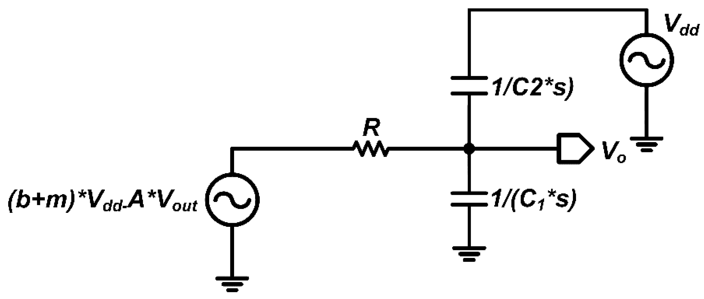
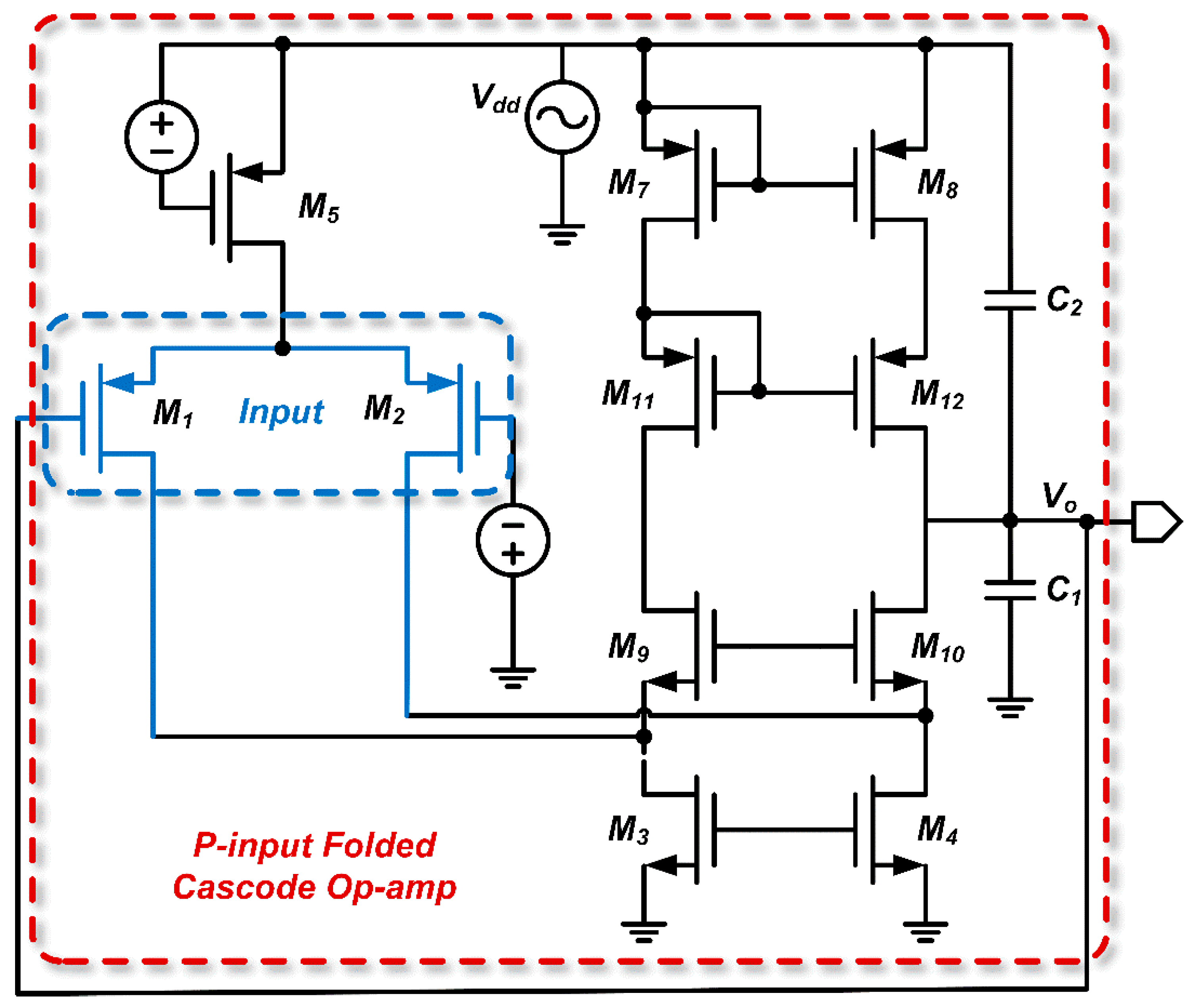
In
Figure 10, the capacitor C2 is a parasitic capacitor located between Vdd and Vo. While it might seem counter-intuitive for achieving high PSRR due to its placement, C2 actually plays a vital role in stabilizing the output voltage Vo by providing a low-impedance path for high-frequency noise and supply-induced disturbances. This helps in filtering out unwanted noise, which is crucial for improving the power supply rejection ratio (PSRR). Among all the parasitic capacitances present in the circuit, C2 is considered the most significant due to its larger capacitance value and strategic position in the feedback loop, which maximizes its positive impact on PSRR enhancement.
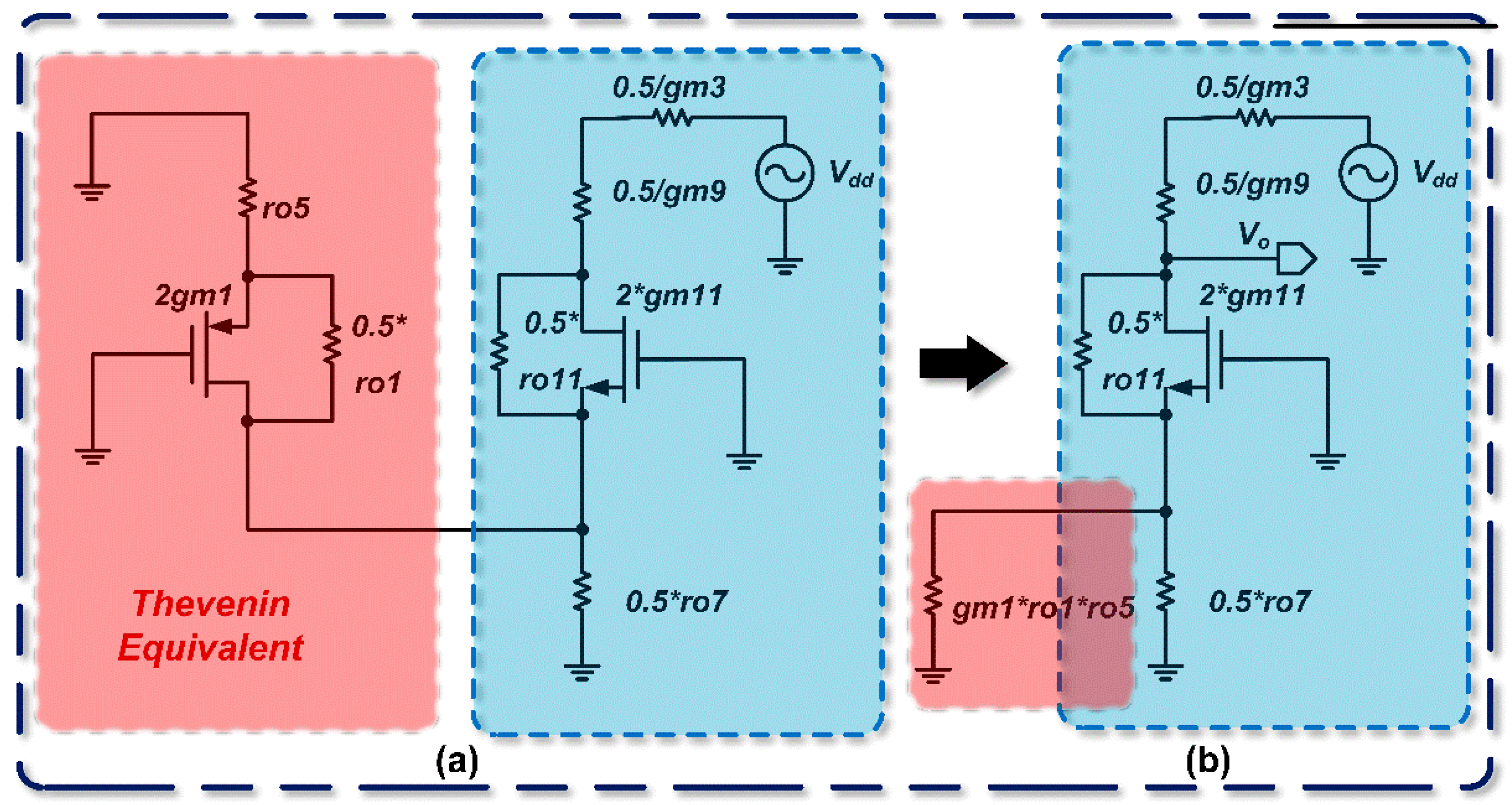
Using the Thevenin theorem, we first derive the open-circuit output voltage of the first stage. This open-circuit voltage can be computed by applying the superposition principle. The analytical approach is similar to that for the P- and N-input two-stage op-amps. First, the effect of the drain input signal from M
5 on the output is calculated. The circuit is modeled using the small-signal equivalent, and further simplified via Norton’s theorem, as shown in
Figure 11, yielding a Thevenin equivalent voltage of
, and:
Next, we calculate the effects of the drain input signals from M
3 and M
4 on the output. The resulting Thevenin equivalent voltage is
.
where it is found that .
Subsequently, the effect of on the output is computed; as shown in Figure 12, the Thevenin equivalent voltage induced by is Finally, by applying the superposition theorem, the circuit is reduced to its simplest form:
Figure 12.
Folded cascode op-amp simplified using the superposition theorem.
Figure 12.
Folded cascode op-amp simplified using the superposition theorem.
denotes the output resistance of the first stage. To calculate the PSRR, the values of
and
must be determined. Based on the circuit diagram, we write the node current equation at
:
In this example,
. The inverse of the DC PSRR value is equal to the op-amp gain. The PGB is then derived as:
Key design insights include:
- a)
Increasing gm1 directly raises the DC PSRR value.
- b)
Reducing the parasitic capacitance C2 improves the frequency response.
- c)
The dominant pole of the op-amp is associated with its output node. Consequently, augmenting C1 shifts this pole closer to the origin, which is advantageous for enhancing both system stability and the frequency response of the PSRR. However, it is crucial to strike a balance with the required bandwidth; one cannot indiscriminately reduce the bandwidth without considering the overall system performance requirements.
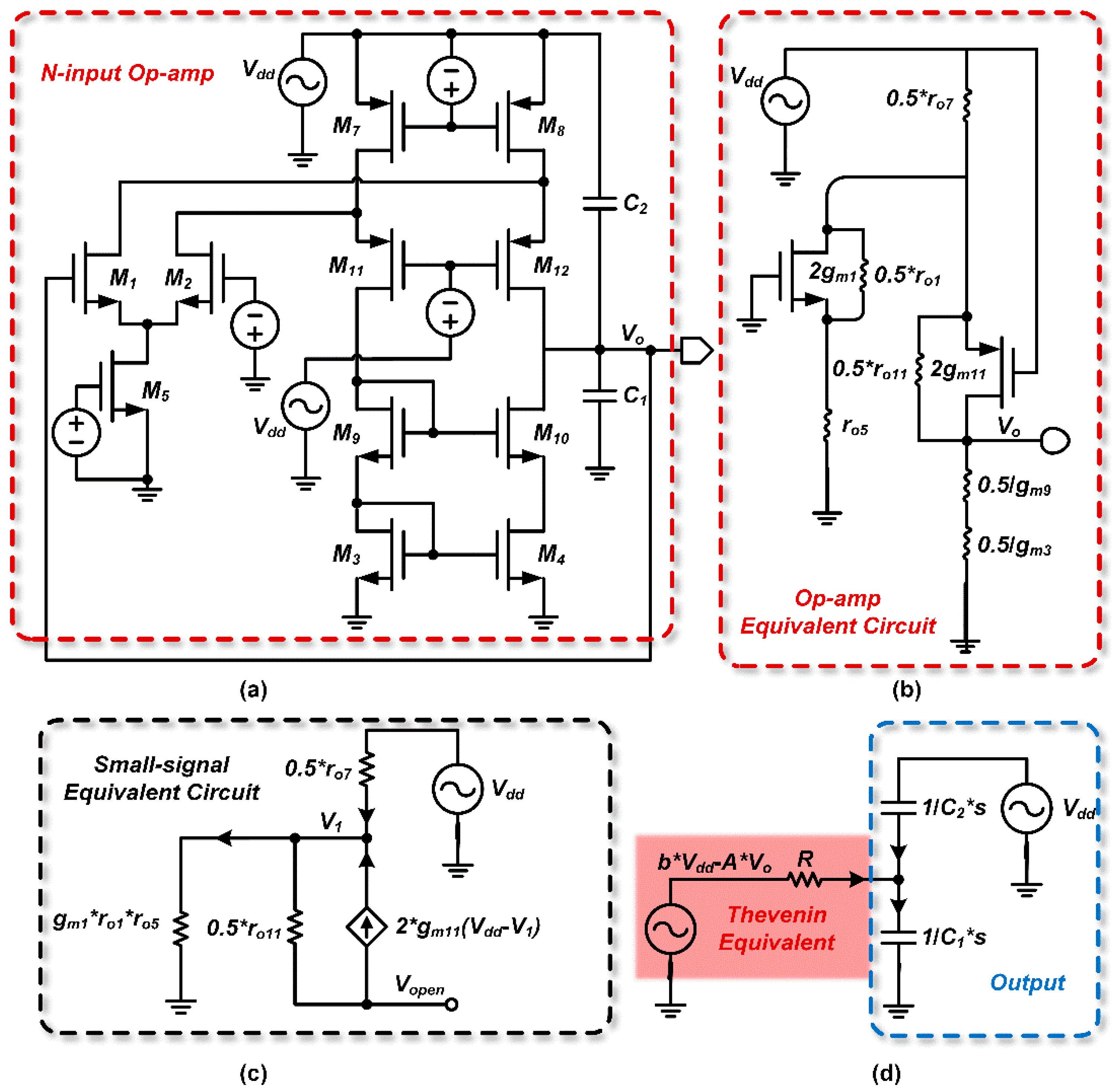
2.2.4. N-Input Folded Cascode Op-Amps
Following the approach in
Section 2.2.3, we analyze the N-input folded cascode op-amp. The simplified flowchart for a typical N-input two-stage op-amp is consolidated in Figure 13
.
Figure 13.
Simplified flowchart for a typical N-input two-stage op-amp
Figure 13.
Simplified flowchart for a typical N-input two-stage op-amp
From the Thevenin equivalent circuit, we obtain:
where the equivalent resistance is
Using resistive voltage division, the Thevenin equivalent voltage is found to be
The Thevenin equivalent voltage induced by
is
:
Where
denotes the output resistance of the first stage. By writing the node current equation at node
, the relationship between
and
is obtained:
Subsequently, the PSRR is calculated as
is the compensation capacitor and
represents the parasitic capacitance. Since the op-amp’s input resistance R is very high, the zero is located near the origin, while the pole is far from the origin:
3. Results and Discussions
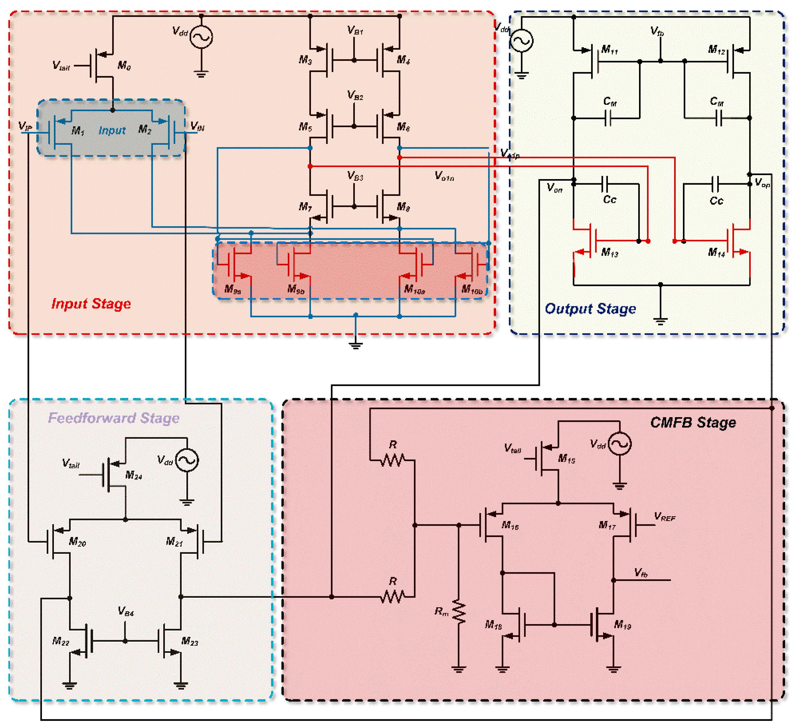
In this section, we will apply the proposed method to design a fully differential op amp with high PSRR. The circuit was designed using Cadence Virtuoso IC617 with a 180 nm CMOS process. We will first list the calculation process of several important indicators, and find the aspect ratio of each transistor through the constraints of multiple indicators. Then compare the simulation results with the calculation results to verify the accuracy of the PSRR calculation method
At the same time, we use the PGB formula to more intuitively know how to improve the PSRR of this complex circuit. We performed a simulation and verified the correctness of the PGB theory by comparing the PSRR before and after the modification.
At the end of this section, the simulation results of the circuit are given, and the expected indicators and the size of each transistor are given in a table at the end of the chapter for reference.
Figure 14.
Circuit architecture.
Figure 14.
Circuit architecture.
- a)
Gain Expression
The transconductance of the input stage, G
m1, is given as:
The voltage gain is expressed as:
- b)
Transfer Function Optimization
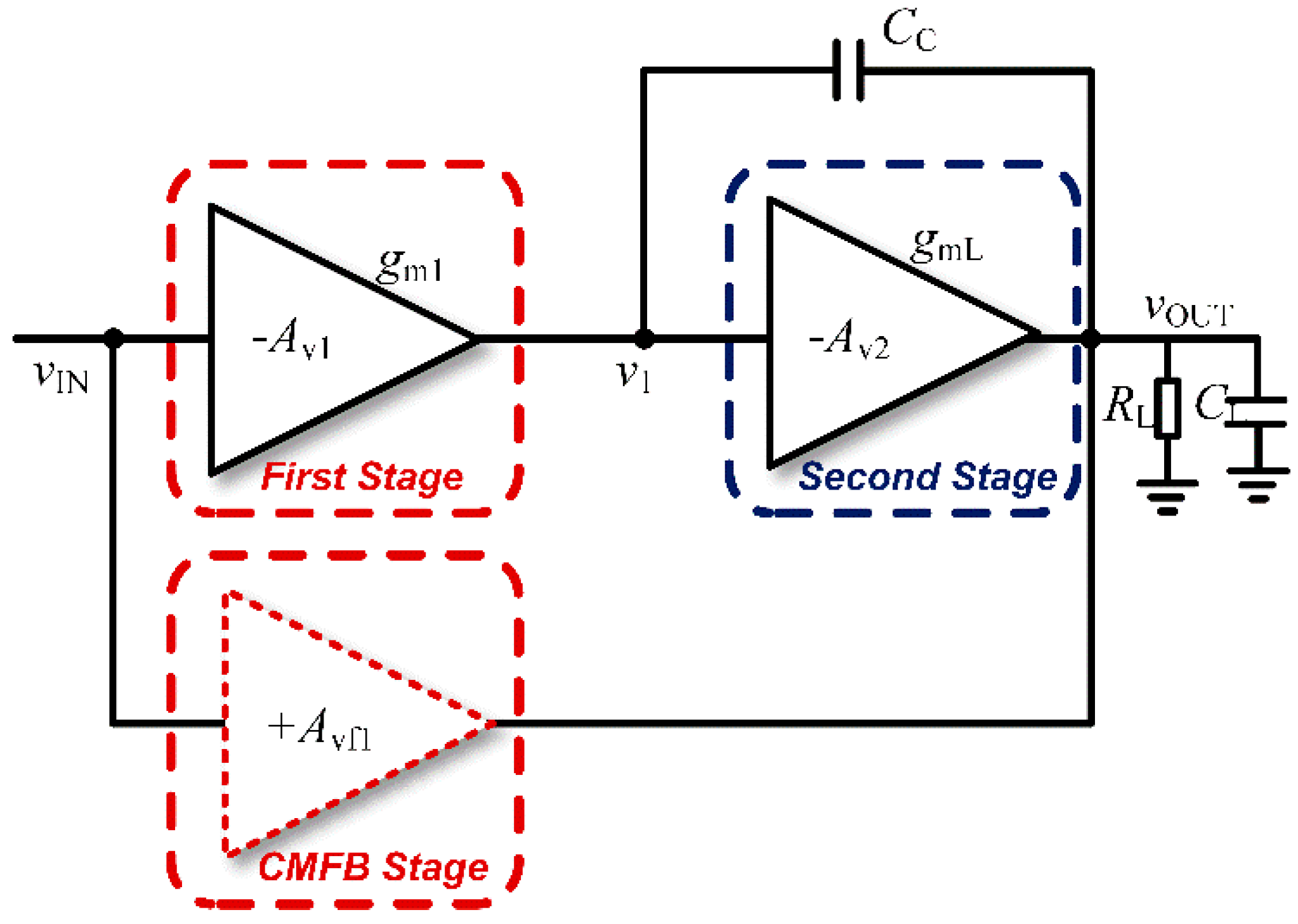
As illustrated in
Figure 15, the feedforward stage introduces a zero-pole pair in the transfer function, compensating for the dominant pole. This minimizes phase lag and extends the high-frequency bandwidth. The transfer function is given by
- c)
PSRR
We calculate the PSRR using the method presented in Chapter II. Referring to
Figure 10. in Chapter II, the first stage of op amps can be equivalent to
, Where:
Referring to the calculation in
Figure 9., replace the original b with here and replace with the transfer function of PSRR that can be obtained directly
Assuming
,
,
,
,
If
,
,
:
Constrained by the above formula, we calculated the initial dimensions by hand, and after several simulation adjustments, we determined the final dimensions of each transistor.
Table 1 shows the design specifications of this circuit.
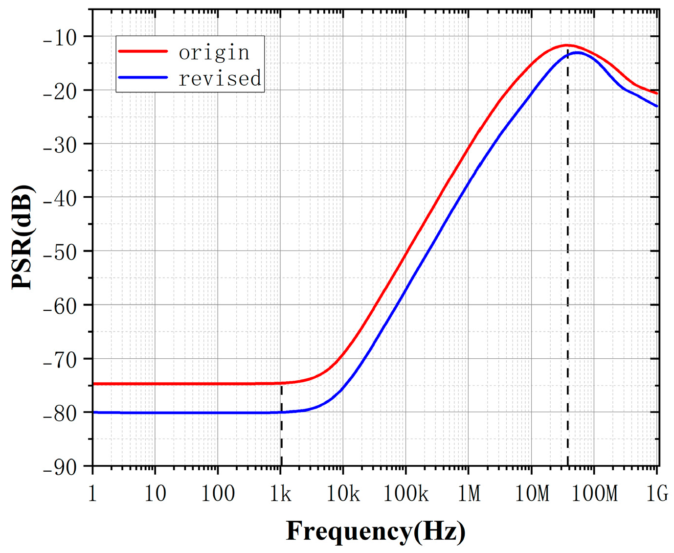
The PSR is defined as the ratio of output voltage change to the power supply perturbation, representing how strongly supply disturbances couple directly into the output. In contrast, the PSRR is commonly defined as the inverse of this ratio or equivalently as the difference between the amplifier's gain and PSR, namely:
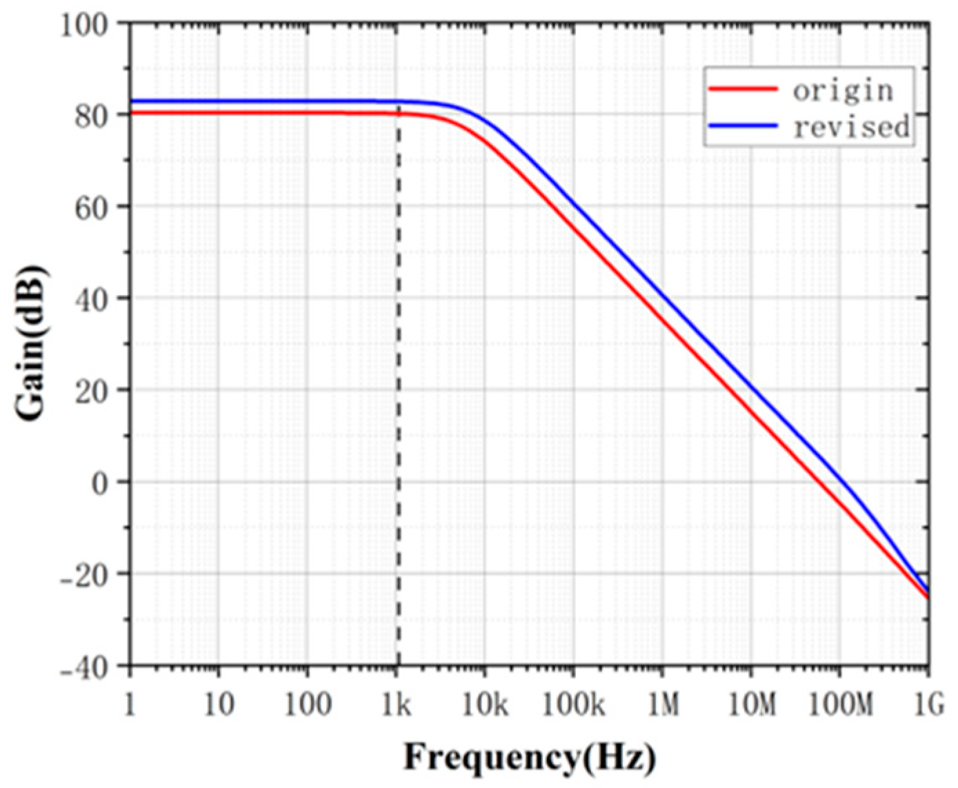
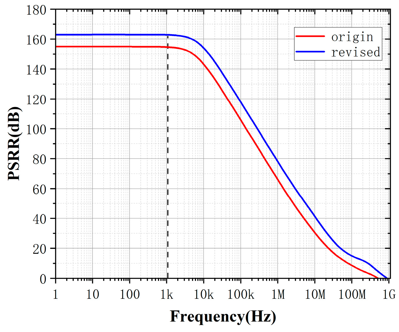
In practical industry designs, PSR is typically of direct concern because it quantifies the amount of power-supply noise propagating into the signal path. However, directly analyzing and optimizing PSR is complicated due to intricate interactions among circuit parameters and the resulting mathematical complexity. Conversely, analyzing both PSR and PSRR—especially using our proposed PGB methodology—are significantly more straightforward and intuitive. By utilizing the PGB framework, we know that we can enhance the performance of PSRR by increasing gm or reducing Cc according to (63). The simulation results before and after the modification are shown below:
Figure 16.
Gain simulation experiment.
Figure 16.
Gain simulation experiment.
As illustrated in
Figure 17 and
Figure 18, by optimizing these parameters through the intuitive guidance provided by PGB, we achieve enhanced PSRR performance. Due to the explicit mathematical relationship between PSRR and PSR, improvements in PSRR obtained via the PGB approach can indirectly yet effectively inform designers how to optimize PSR performance. This demonstrates the practical advantage of using the PGB metric as an intuitive design tool, bridging the gap between complex PSR calculations commonly faced in industrial practice and straightforward PSRR optimizations.
We also performed some other simulations on the circuit.
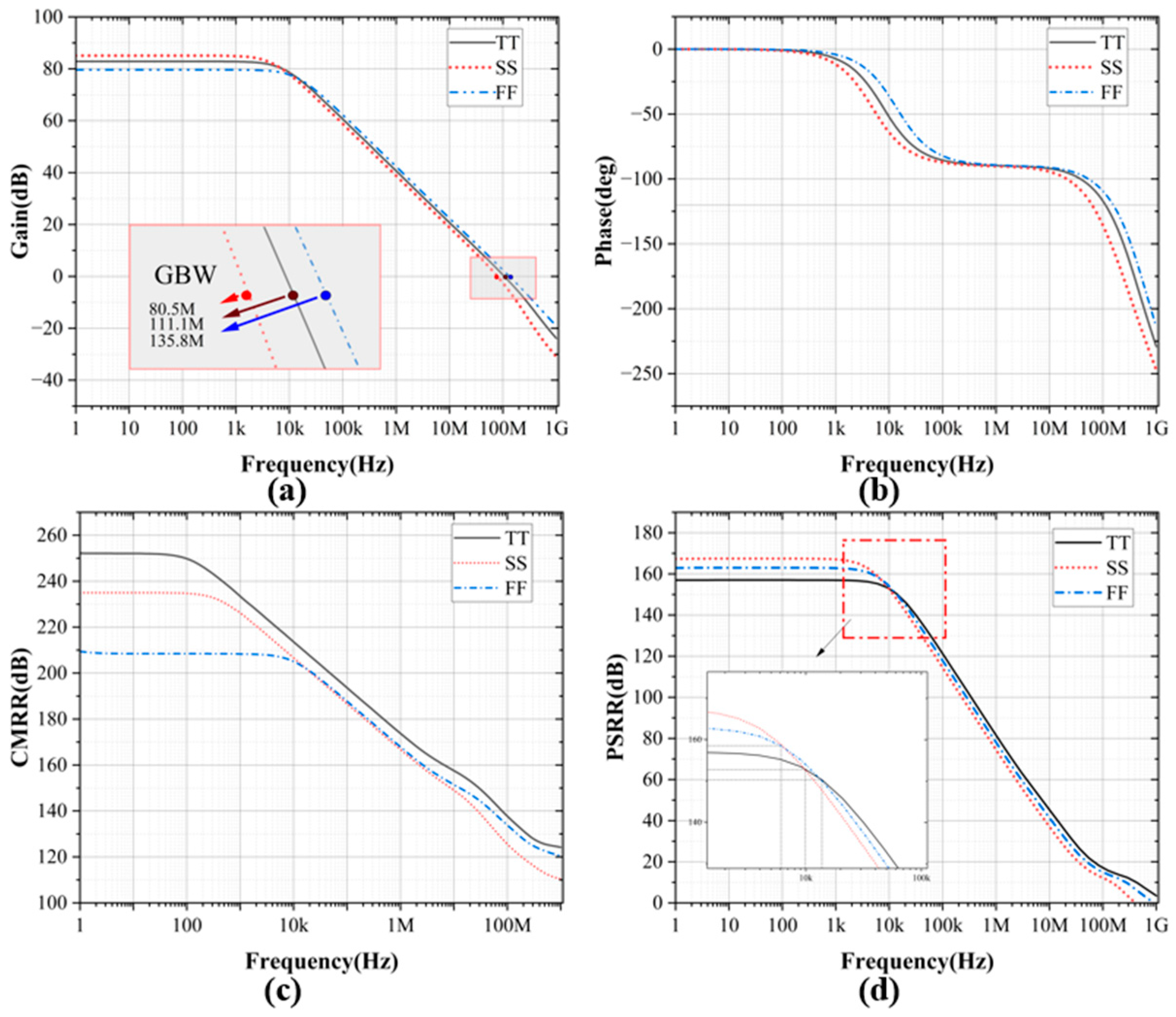
Figure 19 shows the basic indicators of the circuit at different process corners, and
Figure 19-d shows the PSRR of the circuit at each process corner after PGB operation adjustment
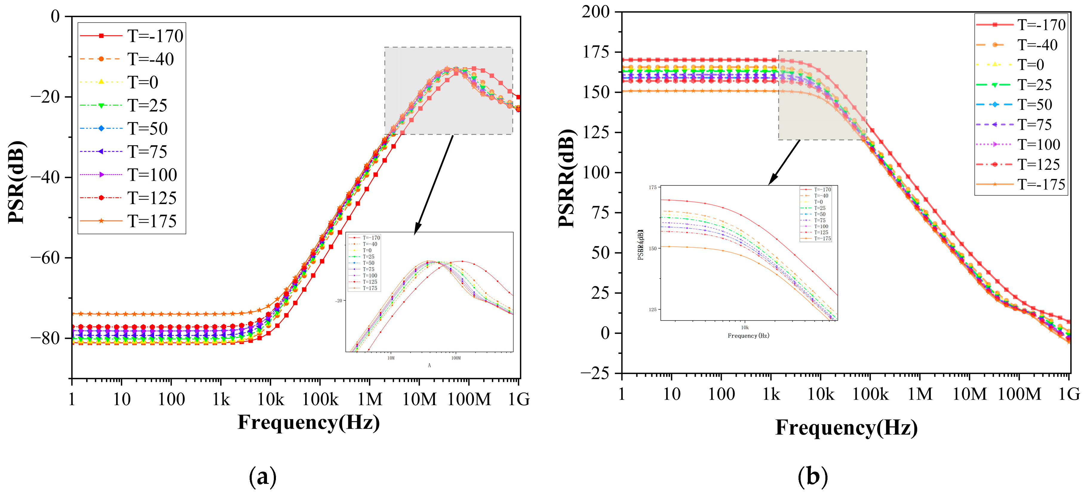
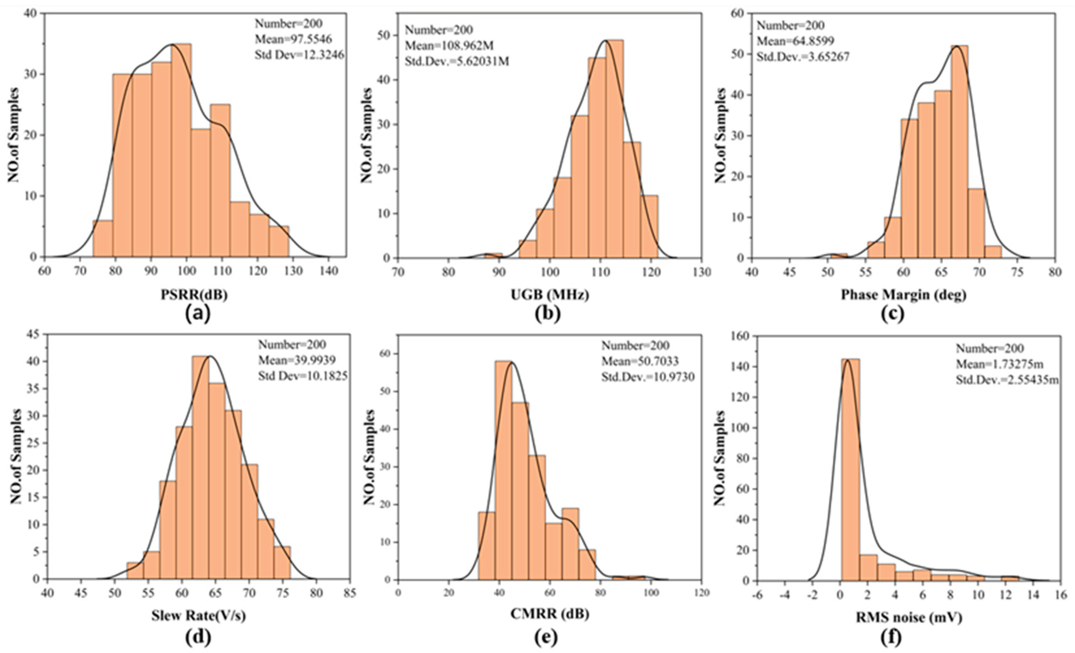
The PSRR of this circuit is more than 155dB at 100kHz for all process conners. It is also very good at high frequencies. We also tested the PSRR and PSR performance of the circuit under different temperature conditions, as shown in
Figure 20. And the results of Monte Carlo simulation are shown in the
Figure 21.
Table 2 shows the simulation results of this circuit and the comparison with other high PSRR op amps.
Table 3 shows the final dimensions of each transistor after re-adjustment according to the PGB method. The design requirements are achieved in all indicators and a good FOM value is achieved. The PSRR calculation method proposed in this article provides a new idea for future circuit design, and the PGB optimization method can also simplify the complex process of PSR calculation.
4. Conclusion
Experimental validation in Section III demonstrates that by leveraging Thevenin’s equivalence principle, the proposed method transforms multi-stage op-amps into simplified black-box models, significantly reducing computational complexity while enhancing intuitive analysis. The introduced PGB metric, which correlates the DC PSRR value with the first dominant pole frequency, eliminates the reliance on exhaustive S-parameter modeling. This enables a computationally efficient evaluation of PSRR performance within the target frequency band. While the PGB framework assumes validity primarily below the GBW—a constraint inherent to its first-order approximation—it remains highly practical for industrial design scenarios where critical PSRR specifications typically reside in low-to-mid frequency ranges. the PGB metric provides actionable insights for optimizing PSRR through parameter adjustments and facilitates rapid comparative analysis of competing circuit topologies.
The proposed framework not only simplifies PSRR analysis for asymmetric and multi-stage circuits but also provides actionable insights for optimizing key parameters (e.g., transconductance, compensation capacitance) to meet stringent industrial requirements. Future work will extend this approach to mixed-signal systems and explore its integration with machine learning-driven design automation tools.
Author Contributions
Conceptualization, Yi Zhang.; methodology, Yi Zhang; software, Yi Zhang; validation, Yi Zhang; formal analysis, Yi Zhang and Ruonan Lin; investigation, Xin Yang and Ruonan Lin; resources, Tailai Li; data curation, Yi Zhang.; writing—original draft preparation, Xin Yang; writing—review and editing, Tailai Li and Jiwei Huang; visualization, Yi Zhang and Xin Yang; supervision, Yi Zhang; project administration, Yi Zhang; Funding acquisition: Jiwei Huang. All authors have read and agreed to the published version of the manuscript.”.
Funding
This research received no external funding.
Data Availability Statement
All data for this article are available.
Conflicts of Interest
The authors declare no conflicts of interest.
References
- J. S. Kim, S. Ha, H. Jeong and J. Roh, "A High-PSRR NMOS LDO Regulator With Intrinsic Gain-Tracking Ripple Cancellation Technique," in IEEE Transactions on Circuits and Systems I: Regular Papers, vol. 71, no. 11, pp. 4951-4960, Nov. 2024. [CrossRef]
- I. Colli-Menchi, J. Torres and E. Sánchez-Sinencio, "A Feed-Forward Power-Supply Noise Cancellation Technique for Single-Ended Class-D Audio Amplifiers," in IEEE Journal of Solid-State Circuits, vol. 49, no. 3, pp. 718-728, March 2014. [CrossRef]
- -C. Chiu et al., "A 0.6 V Resistance-Locked Loop Embedded Digital Low Dropout Regulator in 40 nm CMOS With 80.5% Power Supply Rejection Improvement," in IEEE Transactions on Circuits and Systems I: Regular Papers, vol. 62, no. 1, pp. 59-69, Jan. 2015. [CrossRef]
- Y. Choi, W. Tak, Y. Yoon, J. Roh, S. Kwon and J. Koh, "A 0.018% THD+N, 88-dB PSRR PWM Class-D Amplifier for Direct Battery Hookup," in IEEE Journal of Solid-State Circuits, vol. 47, no. 2, pp. 454-463, Feb. 2012. [CrossRef]
- K. A. I. Halonen, W. M. C. Sansen and M. Steyaert, "A micropower fourth-order elliptical switched-capacitor low-pass filter," in IEEE Journal of Solid-State Circuits, vol. 22, no. 2, pp. 164-173, April 1987. [CrossRef]
- Razavi B .Design of analog CMOS integrated circuits[J].2001.
- P. E. Allen, D. R. Holberg, "CMOS Analog Circuit Design," 2nd ed., Beijing: Publishing House of Electronics Industry, 2005, pp. 232–234.
- P. R. Gray, P. J. Hurst, S. H. Lewis, and R. G. Meyer, Analysis and Design of Analog Integrated Circuits, 4th ed., Beijing: Higher Education Press, 2005, pp. 410–415.
- J. S. Kim, S. Ha, H. Jeong and J. Roh, "A High-PSRR NMOS LDO Regulator With Intrinsic Gain-Tracking Ripple Cancellation Technique," in IEEE Transactions on Circuits and Systems I: Regular Papers, vol. 71, no. 11, pp. 4951-4960, Nov. 2024. [CrossRef]
- H. Zhang, N. N. M. Rozsa, M. Berkhout and Q. Fan, "A Chopper Class-D Amplifier for PSRR Improvement Over the Entire Audio Band," in IEEE Journal of Solid-State Circuits, vol. 57, no. 7, pp. 2035-2044, July 2022. [CrossRef]
- Yang, K. Ye and M. Tan, "A 0.5-V Capless LDO With 30-dB PSRR at 10-kHz Using a Lightweight Local Generated Supply," in IEEE Transactions on Circuits and Systems II: Express Briefs, vol. 67, no. 10, pp. 1785-1789, Oct. 2020. [CrossRef]
- Sumit Kumar and R. K. Sharma, "A cross-coupled cascode feedback design of an area-efficient frequency compensated OTA," in Arabian Journal for Science and Engineering, vol. 49, pp. 6305-6317, 2024. [CrossRef]
- Ghader Yosefi, "A special technique for Recycling Folded Cascode OTA to improve DC gain, bandwidth, CMRR and PSRR in 90 nm CMOS process," in Ain Shams Engineering Journal, vol. 11, pp. 329-342, 2020. [CrossRef]
- Seyed Vahid Feizbakhsh and Ghader Yosefi, "An enhanced fast slew rate recycling folded cascode Op-Amp with general improvement in 180 nm CMOS process," in International Journal of Electronics and Communications (AEÜ), vol. 101, pp. 200-217, 2019. [CrossRef]
- Montree Kumngern, Tomasz Kulej, and Fabian Khateb, "31.3 nW, 0.5 V Bulk-Driven OTA for Biosignal Processing," in IEEE Access, vol. 11, pp. 56516-56525, 2023. [CrossRef]
|
Disclaimer/Publisher’s Note: The statements, opinions and data contained in all publications are solely those of the individual author(s) and contributor(s) and not of MDPI and/or the editor(s). MDPI and/or the editor(s) disclaim responsibility for any injury to people or property resulting from any ideas, methods, instructions or products referred to in the content. |
© 2025 by the authors. Licensee MDPI, Basel, Switzerland. This article is an open access article distributed under the terms and conditions of the Creative Commons Attribution (CC BY) license (http://creativecommons.org/licenses/by/4.0/).
