Submitted:
02 September 2025
Posted:
03 September 2025
You are already at the latest version
Abstract
With the continuous scaling of semiconductor process nodes toward 3 nm and beyond, traditional optical proximity correction and resolution enhancement technologies are increasingly challenged by the physical limits of sub-wavelength lithography. Inverse lithography technology, as a core branch of computational lithography, has emerged as a pivotal solution to break through these constraints. This review focuses on inverse lithography technology in integrated circuit manufacturing. It begins with an introduction to the key position of lithography and the background of inverse lithography. Then, it elaborates on the working principle, research progress, technical advantages, challenges, and future development directions of inverse lithography technology. By integrating relevant research findings, this paper provides a comprehensive understanding of inverse lithography technology, aiming to offer valuable insights for further research and application in this field.
Keywords:
inverse lithography technology
; computational lithography
; process window
; pattern fidelity
1. Introduction
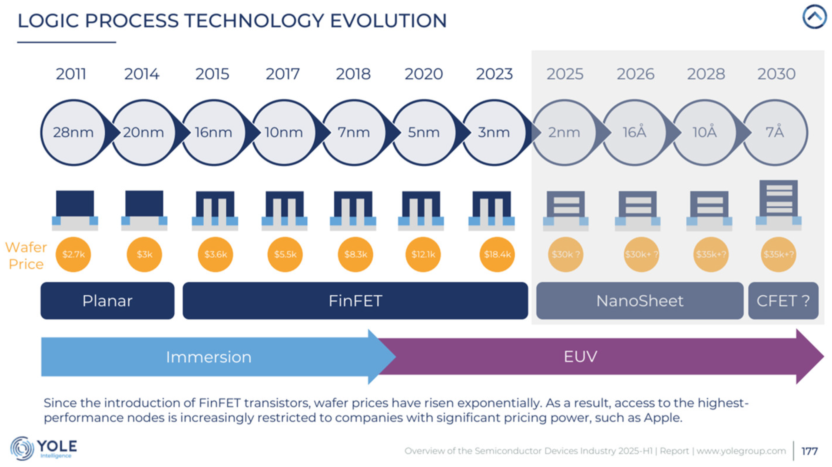
Lithography is the core technology in integrated circuit (IC) manufacturing, playing a crucial role in determining the performance, cost, and miniaturization of ICs [1]. It is used to transfer the circuit pattern on the mask to the semiconductor substrate, enabling the precise fabrication of various components in the IC. The continuous development of lithography technology has been a major driving force behind the miniaturization and performance improvement of ICs. According to the YOLE Intelligence [2] report, as the feature size of ICs continues to shrink, the requirements for lithography technology become more stringent. When the minimum line width in the device is smaller than the exposure wavelength of the lithography machine, diffraction and interference effects of adjacent patterns can cause distortion of the image on the wafer, known as optical proximity effect (OPE). The practice of correcting the pattern on the mask appropriately to obtain the same pattern as the design on the wafer is called optical proximity correction (OPC).
Figure 1.
Logic process technology evolution [2].
Figure 1.
Logic process technology evolution [2].
As illustrated in Figure 2 [3], the requirements for mask correction have evolved across different technological eras, driven by advancements in semiconductor manufacturing and increasingly stringent performance demands. Overall, OPC technology has undergone a progressive refinement, transitioning roughly through four distinct generations: rule-based OPC (RB-OPC), model-based OPC (MB-OPC), rule/model-based sub-resolution assist feature (SRAF) insertion, and model-driven pixel-level optimization employed in inverse lithography technology (ILT). This evolution has been accompanied by a corresponding increase in algorithmic and computational complexity.
The earliest iteration, RB-OPC, operated on predefined correction heuristics applied globally to mask layouts. These rules typically established bias tables based on critical geometric attributes such as line width and pitch, enabling automated modification of qualifying patterns through edge-displacement operations—a technique known as edge-based correction. A significant advancement came with the integration of SRAF into RB-OPC frameworks: by inserting sub-resolution auxiliary features (typically linear or block-shaped structures), the process window for semi-isolated and isolated patterns was substantially expanded. Despite their simplicity, RB-OPC and rule-based SRAF methodologies remained effective solutions for mitigating OPE.
As IC technology advanced to finer process nodes, shrinking critical dimensions (CDs) and increasingly complex pattern topologies necessitated more sophisticated correction approaches, leading to the development of MB-OPC. This paradigm shift introduced lithographic imaging models—incorporating both optical and photoresist response physics—thereby framing OPC as a mathematical optimization problem for mask patterning. Leveraging computational optimization algorithms, MB-OPC calculates optimal mask geometries by minimizing edge placement error (EPE), defined as the Euclidean distance between model-predicted contours and target layouts at pre-specified evaluation points. The direct correlation between minimized EPE and improved pattern fidelity makes it the primary cost function in modern model-based correction workflows [4].
ILT has emerged in response to the challenges faced by traditional lithography techniques as the feature size of ICs continues to shrink [5]. When the feature size of ICs is reduced to 45 nm or less, the complexity of OPE greatly increases. The correction strategy based on line segment displacement will be limited by the topology and inherent layout of the original layout, and its potential solution space will become limited, making it difficult to obtain ideal correction results [6]. ILT begins by discretizing the mask into pixel arrays, obviating the need for manual segmentation of polygons edges in mask. Subsequently, via iterative mathematical computations, the pixelated mask undergoes evolution along the gradient descent direction of the lithographic error function, continuing until the function reaches convergence. By breaking free from the topological constraints inherent in the original design layout, ILT exhibits greater flexibility compared to the edge-segmentation-based correction strategies of conventional OPC. This enhanced flexibility enables ILT to achieve superior imaging fidelity and a more expansive process window in advanced lithographic applications [7].
2. The Working Principle
2.1. The Basic Concepts and Processes
Lithography is a key procedure in the manufacturing process of ICs, and its resolution and accuracy significantly impact the performance of the microelectronic devices. With the development of semiconductor technology and the continuous improvement of technology nodes, especially when the technology nodes are less than 90 nm [8], the impact of the OPE on the lithography process is becoming increasingly evident. Therefore, it has become a key issue to narrow the gap between the lithography process control capability and the lithography process window and enhance the efficiency and performance of the lithography process.
Currently, for mitigating the impact on OPE, MB-OPC has become a standard practice [9]. In MB-OPC, the mask is first segmented into a series of movable line segments according to pre-defined rules. Lithography simulations are then performed on the mask, and the line segments are iteratively adjusted based on simulation results to correct pattern distortions. However, as the feature size of ICs shrinks to 45 nm and below, the complexity of OPE increases significantly. Traditional correction strategies based on line segment displacement face limitations imposed by the original layout topology and fixed design constraints, leading to a constrained solution space that struggles to achieve optimal correction results.
AS a novel resolution enhancement technique (RET), ILT can achieve higher imaging quality and a larger process window [10]. The strategy of ILT is to pixelate the layout and then optimize the position and size of each pixel to obtain the best results. Thus, ILT is known as pixel based OPC (PB-OPC). The advantage of this method is that it does not have the limitation based on fixed line segment displacement in traditional OPC. By directly processing pixels instead of moving line segments, ILT provides greater flexibility in layout modification, enabling it to cope with more complex OPE [11].
The workflow of mask pattern generation using ILT is illustrated in Figure 3. The process commences with defining inputs such as the target pattern, illumination source parameters, and initial mask configuration, followed by constructing a pixelated mask model. A lithography model is then established to simulate the aerial image formation, where the sigmoid function is typically employed to characterize the photoresist threshold behavior. This allows the prediction of the latent image profile on the photoresist.
Subsequently, a cost function (CF) is formulated to quantify the discrepancy between the simulated wafer image and the target pattern. The choice of optimization algorithm hinges on the nature of the CF: for continuously differentiable formulations, gradient-based methods are commonly adopted to navigate the solution space. Advanced variants such as steepest descent, momentum-based optimization, adaptive gradient, and adaptive moment estimation offer distinct strategies to enhance convergence speed and stability. The method of iteration is used to correct a mask according to the set step length after calculating the optimization direction for each iteration until the satisfactory mask is found. The CF can include many additional elements, such as mask manufacturing error and its impact on wafer printing [12]. For example, in level-set-based inverse lithography, the inverse lithography problem is addressed as an obstacle reconstruction problem or an extended nonlinear image restoration problem, and then solved by a level set time-dependent model with finite difference schemes [13].
2.2. Mathematical Description and Algorithms
Mathematical description and algorithms are at the heart of ILT. The imaging model of optical lithography is the foundation for developing inverse lithography algorithms. It describes the relationship between the mask pattern, illumination source, and the resulting image on the resist. When ILT is used to calculate the mask, pattern required by the target layout, a pair of mathematical expressions of the inverse problem are usually used to describe this process [6]:
where Litho() represents a forward lithography calculation function, which can be calculated using a lithography simulation system. Mask is the mask image, and contour is the wafer image generated by lithography simulation. Litho-1() represents its inverse function, z is the original design layout, i.e., the target layout, and mask* is the corresponding mask when the contour of lithography result is z. If the expression of Litho-1() can be obtained, the solution mask* for inverse lithography can be directly calculated.
During the inverse lithography process, the CF serves as an optimization criterion, guiding iterative mask modifications to minimize discrepancies between simulated and target patterns. The basic form of a CF in ILT is shown below [14]:
And this CF can be extended to capture many process conditions, for example:
In this context, (actual – goal) mathematically defines the spatial error metric between the simulated pattern and the target specification. The topological weight Wp allows for attribute-specific weighting, where critical features can be assigned higher weights to prioritize their accuracy, pw represents the multiple process window conditions.
ILT employs gradient-based optimization by computing ∂Cost/∂Mask to derive the optimal global mask modifications that minimize the lithographic CF. The mask undergoes iterative updates according to the equation below, where the gradient Gm is scaled by a damping factor to ensure numerical stability and convergence.
It should be noted that this overview represents a highly simplified approximation of ILT; for a more rigorous and comprehensive mathematical formulation, readers are referred to the extensive body of literature on this subject, e.g., [15,16,17,18].
In terms of algorithm development, new algorithms have been proposed to improve the computational efficiency and imaging performance of ILT. For example, a fast inverse lithography based on dual-channel model-driven deep learning (DL) method has been developed. The architecture of the DMDL network is derived from the inverse optimization model under a gradient-based ILT framework. A dual-channel structure is introduced to simultaneously modify the mask contour and insert SRAFs, improving the lithography image fidelity. An unsupervised training strategy based on auto-decoder is developed to avoid the time-consuming labelling process. The superiority of DMDL over the state-of-the-art ILT method has been verified in both computational efficiency and image fidelity obtained on the semiconductor wafer [19]. In the area of multi-objective optimization, multi-objective ILT and the hybrid dynamic priority (HDP) algorithm have been investigated and developed. High-performance images with high fidelity and high uniformity have been obtained at multi-field and multi-clip areas across the die. The HDP algorithm can improve the uniformity of images at full-field points by up to 31.1% compared to current multi-objective optimization algorithms in the case of multi-field wave front error-aware SMO [5]. Furthermore, in the application of ILT in different lithography systems, such as extreme ultraviolet lithography (EUVL), researchers have designed masks using ILT to correct for aberrations in a single-spherical-mirror projection optical system. By using ILT implemented by an adjoint-based gradient descent optimization algorithm, test patterns can be successfully printed despite large spherical aberrations [20].
In 1981, ILT was first proposed by B. E. A. Saleh and S. I. Sayegh [21]. A few years later, Saleh and Nashold [22] described an algorithm using a sequence of projection operators to find a band-limited function, corresponding to a continuous-tone or gray-scale mask that optimized the desired image. At the beginning of the development of ILT, Pati et al. [23] proposed the projection onto convex sets (POCS) algorithm, which is rooted in convex set optimization theory, to mitigate image distortion induced by binary masks and phase-shift masks. Meanwhile, Sherif et al. [24] proposed a binary mask optimization method based on incoherent diffraction lithography system, which expresses the ILT as mixed-integer linear programming and solves it through branch-and-bound method. Furthermore, random-pixel programming [25], genetic algorithm [26] and nonlinear programming [27] discrete algorithms have been proposed one after another to solve ILT related problems.
However, discrete methods have inherent limitations: due to the fact that discrete optimization only optimizes in discrete space, the entire optimization process may not converge stably, and there may be problems with slow convergence speed [6]. Amyn Poonawala et al. [28] first converted this discrete optimization problem into a constrained continuous one, and further transformed it into an unconstrained continuous optimization problem by introducing intermediate variables. Once unconstrained, it can be solved using various continuous optimization algorithms like gradient descent. Recently, Ma et al. [29] proposed a better solution for multi-patterned mask design by simultaneously optimizing masks and decomposing layouts. Yu et al. [30] introduced the Adam search algorithm into gradient-based methods. Compared to the commonly used stochastic gradient descent (SGD), this algorithm adjusts the learning rate during random search by calculating the first and second moments of the gradient, achieving faster convergence.
On the other hand, more accurate corrections rely on more precise simulations. Kosta Selinidis et al. [14] integrated rigorous simulation into ILT, they indicated that a rigorous mask 3D model component is a very important part of the rigorous simulation. As is well known, for full rigorous simulation, the biggest hurdle is computing time. However, the Sentaurus Lithography (S-Litho) rigorous simulation tool has adopted a new M3D rigorous modeling approach. This approach integrates an advanced optimization mode, enabling a computation acceleration ranging from 5 to 100 times.
2.3. Four Mainstream Implementation Methods
2.3.1. Level-Set Method
One important method about ILT is level-set method, which proposed by Stan Osher and James Sethian [15] in 1988. Luminescent first applies level-set method to ILT to solve the ILT runtime problem [16,31,32,33,34]. The goal of the level-set method is to minimize CF by reducing the number of variables and solving topological discontinuities. The main idea of the level-set method is to convert a 2D closed curve into a 3D surface, treating the 2D closed curve as a set of intersection lines between the 3D surface and the zero plane, hence it is called a level-set. Starting in 2003, Luminescent developed an ILT approach based on the level-set method, aiming to enhance mask optimization efficiency, reduce complexity, and thereby shorten runtimes [10].
As shown in Figure 4, a distance function can be defined such that, for any point (x, y), its value (z) corresponds to the shortest distance from that point to the nearest edge of the 2D curve. The surface represented by this function intersects the xy-plane in a 2D shape, and this shape at the zero level-set (on the xy-plane) is exactly the original 2D curve [10].
The level set mathematical method solves the problem of 2D curve evolution. When designing the ILT algorithm, the lithography model is used to determine the optimization direction and velocity of each point on the mask, and the level set is used to achieve the evolution of the mask [35].
As shown in Figure 5, a main pattern (a contact hole in this case) on the mask exhibits 2 SRAFs by raising the surface around the main contact hole during the optimization process, which undergoes a sudden change in the evolution of the 2D curve from 1 closed curve to 3 closed curves, while the constructed 3D surface remains a continuous surface. When the surface passes through the plane corresponding to a level of zero (the xy plane), the SRAFs appear. Construct a 3D surface using the level-set method, and transform the lithography pattern composed of closed curves into the intersection line between the surface and the zero-value plane. The emergence of SRAF makes 2D functions discontinuous. By using the level-set method to transform them into 3D surfaces that can be continuous, ILT optimization can be expressed as a general multivariate optimization problem and solved using standard optimization algorithms such as conjugate gradient method.
2.3.2. Intel Pixelated ILT
Another ILT method is the Intel pixelated ILT. The Intel pixelated ILT Method, introduced in 2007, represents a significant advancement in lithography optimization [36]. This approach utilizes alternating phase-shift masks (Alt-PSMs) to enhance resolution and employs a pixel-based design to satisfy mask rules and reduce computational complexity. Unlike previous methods that focused on pattern edges, Intel’s method simplifies the problem by mapping the design onto large pixels with only two degrees of freedom (0° and 180° phase shifts). This reduction in complexity allows for more efficient computation while maintaining pattern fidelity and symmetry.
The specific operation steps are shown in the following figure (Figure 6). The process begins with importing an initial layout, which comprises polygons on a target layer. Subsequently, a phase-coloring algorithm is applied to these polygons, with the aim of maximizing patterning accuracy. It should be noted that phase conflicts may arise from the phase-coloring algorithm; here, pixel optimization is employed to address such conflicts. Following this, the polygons are converted into a pixelated form based on a fixed pixel grid. These pixels then undergo an iterative optimization process, ultimately leading to a converged pixel layout, as illustrated on the right side of Figure 6 [36].
Despite its advantages, the Intel method faced challenges, particularly with pixel size limitations. The 100 nm pixel size on the mask, while smaller than the 193 nm wavelength, introduced strong 3D mask effects, especially for Alt-PSMs. To address this, Intel developed a rigorous 3D mask model. Additionally, the method required significant computational resources, necessitating innovations like GPU acceleration and stitching techniques to manage full-chip designs. Intel also demonstrated the practicality of its approach by successfully tape out an experimental mask for a 65 nm node microprocessor, achieving yields comparable to conventional production methods.
The Intel pixelated ILT method laid the groundwork for future advancements, including the integration of multibeam mask writers and GPU-accelerated computing. These innovations not only addressed runtime and mask writing challenges but also paved the way for the adoption of curvilinear ILT solutions in production environments. The method’s success in improving process windows and reducing defects underscored its potential for addressing the complexities of advanced semiconductor manufacturing.
2.3.3. Calculating Curvilinear ILT in Frequency-Domain
Another ILT method is about calculating curvilinear ILT in frequency-domain. The Gauda/D2S [37] approach to ILT represents a significant advancement in the field, leveraging GPU acceleration and a band-limited frequency-domain method to overcome traditional challenges in ILT implementation. Unlike the Luminescent level-set method and the Intel pixelated approach, which operate in the real domain, Gauda/D2S introduced a novel optimization framework that solves the ILT problem in the frequency domain. The method involves transforming the mask from the spatial domain to the frequency domain, performing lithography model calculations in the frequency domain, and using the closed form integral modeling provided by the Hopkins formula to transform the equation into a four-dimensional convolution between the optical system transfer function and the mask function M. The time-domain convolution is equivalent to frequency-domain multiplication, and the convolution operation is transformed into Fourier transform and multiplication operations that are more suitable for parallel operations. If the CF is modified in frequency domain optimization, all symmetric and repetitive patterns will be modified in the same way, thus naturally maintaining symmetry. The conversion of complex convolution calculations into multiplication calculations in the frequency-domain can significantly reduce computational complexity and can be accelerated using GPU [12].
The D2S solution builds on Gauda’s foundational work, which was acquired by D2S in 2014 [10]. This approach employs a comprehensive hardware/software system, including a purpose-built GPU-accelerated computation platform (CDP), designed specifically for ILT. The use of GPU acceleration enables the system to handle the intensive computational demands of ILT, significantly reducing runtime. Combined with the introduction of multibeam mask writers, which write in the pixel domain and are shape-agnostic in terms of write time, the D2S method achieves practical runtimes and mask write times. This breakthrough makes full-chip, curvilinear ILT a reality, addressing the long-standing issues of excessive computational time and impractical mask write times.
The Gauda/D2S method also integrates mask-rule checking (MRC) to ensure that the final ILT masks meet manufacturing requirements, correcting any features that violate minimum dimensions [38]. By maintaining symmetry and avoiding small features, the approach not only improves lithographic results but also enhances mask manufacturability. As shown in Figure 7, the system demonstrated exceptional performance, producing full-chip ILT solutions within a day or two, with process-window improvements exceeding 100% [38]. This development marks a pivotal moment in the history of ILT, transitioning it from an academic concept to a practical production reality.
2.3.4. ILT Method Combined with Machine Learning
The three methods mentioned above generally suffer from the problem of high computational complexity and are difficult to apply widely. In recent decades, with the maturity of machine learning technology, relevant industries or academia are concerned about exploring the integration of machine learning techniques with ILT to mitigate the inherent computational challenges of traditional ILT methods. Conventional ILT approaches are known for their high computational intensity, which has constrained their broader adoption in semiconductor manufacturing workflows. In response, recent research efforts have focused on synergizing machine learning with ILT, aiming to enhance computational efficiency while preserving or even improving the quality of optimization outcomes. This fusion of techniques represents a strategic shift toward addressing the scalability limitations of ILT in advanced technology nodes, and it have gradually become one of the main trends in the future development of ILT.
Luo [39] first attempt to use a multi-layer perceptron combined with artificial neural networks to predict mask patterns. Luo et al. [40] proposed a solution by a support vector machine (SVM)-based layout retargeting method is proposed to generate a high-quality initial input mask for ILT, aiming to accelerate optimization convergence. Kumar et al. [41] proposed a hybrid OPC processing method based on clustering algorithm, which reduces the total simulation time compared to traditional methods. Model-driven convolutional neural networks (MCNN) derive from foundational ILT models, constructing network architectures by unfolding and truncating ILT iterations, and utilize lithography imaging models as decoders for unsupervised training [12,42]. Jiang et al. [43] present a fast machine learning-based mask printability prediction framework that significantly accelerates the OPC process while ensuring comparable or improved printability performance compared to previous methods. Compared to traditional machine learning methods, DL has demonstrated significant advantages in automated feature extraction, big data processing, and nonlinear prediction tasks, and has better potential for application in ILT [6].
In the related research of applying DL to ILT, ASML Brion was one of the first attempts to apply DL to ILT, and in their 2017 paper, they demonstrated a free-form ILT engine that uses CNN to train an ILTDL model, as shown in Figure 8. Firstly, obtain the DLILT model through training; Then, the initial SRAF layout was generated using the DL model and optimized as the initial input layout for the ILT engine. The results showed that using the DL generated initial SRAF method can significantly reduce the overall SRAF generation computation time [44]. Shi et al. [45] developed an optimal feature vector automatic design approach based on CNNs, which serves to reduce errors during the feature extraction phase. Ye et al. [46] put forward a lithography model grounded in generative adversarial networks (GANs), enabling rapid prediction of lithography contours from masks. Kumar et al. [47] adopted a multi-stage regression method to enhance the accuracy of lithography models. More recently, Zhong et al. [48] proposed a CNN-based model for layout decomposition and quality prediction, which was incorporated into an efficient collaborative optimization framework integrating layout decomposition and inverse lithography.
Moreover, Zhang et al. [49] used variational autoencoder (VAE) for mask design, improving the model’s generalization ability and stability through regularization terms and Bayesian inference. Zhao et al. [50] proposed a CNN network based on self-calibrated convolution optimization to improve the computational efficiency of ILT. The self-calibrated convolution enables adaptive encoding of long-range relevant information at each position. Yang et al. [51] develop a GAN model with OPC-oriented flow, ILT pre-training, and enhanced generator to improve mask optimization, reducing OPC steps and boosting printability. Chen et al. [52] present DAMO, a deep learning-enabled full-chip OPC system with DLS, DMG, and a custom layout splitting algorithm, outperforming state-of-the-art academic and industrial solutions.
Zuoxian Chen [6] proposes (in his thesis) GAN-based inverse lithography algorithms to accelerate ILT, enhance lithography quality, and improve mask manufacturability, with three key efforts. First, a Pix2Pix network-based algorithm is presented, which learns layout-to-mask mapping during training to generate quasi-optimal masks quickly in generation. A redesigned Res-UNet generator alleviates gradient vanishing. Experiments, including on the IBM industrial dataset, show 58.5% less runtime, 7.9% lower L2 error, and 4.1% reduced PV-Band versus traditional gradient-based ILT. Second, a detail-enhanced DePix2Pix network is proposed, featuring an ASPP_UNet3+ generator for multi-scale feature fusion, multi-scale discriminators to boost detail generation, and a hybrid loss function for stable training. It further reduces runtime by 6.4%, L2 error by 4.2%, and PV-Band by 3.9% compared to Pix2Pix, with better scalability on complex layouts. Third, a manufacturability-optimized algorithm is developed, using gradient-based ILT with a complexity penalty term for pre-training, integrating the CBAM attention module and a complexity penalty loss. On the IBM dataset, it cuts mask fracturing shots by 31.1% versus DePix2Pix, with only 1.1% higher L2 error and 1.3% larger PV-Band, balancing lithography quality and manufacturability effectively.
3. Progress in Research on ILT
3.1. Evolution of Lithography Techniques
Lithography accounts for 30% to 40% of the manufacturing cost of ICs, and is the most complex, expensive, and critical step in the IC manufacturing process [6]. The semiconductor industry has witnessed a continuous evolution of lithography techniques over the years. Early lithography techniques, such as optical lithography, were based on the use of visible or ultraviolet light to transfer patterns onto the semiconductor substrate. However, as the demand for smaller feature sizes increased, new techniques were developed.
EUVL emerged as a promising technology for the next-generation semiconductor manufacturing. EUVL uses extreme ultraviolet light with a wavelength of 13.5 nm, enabling the fabrication of features with sub-10 nm half-pitches. This technology has the potential to extend Moore’s law and meet the requirements of advanced IC manufacturing [1]. Electron beam lithography (EBL) is another important technique that offers high-resolution patterning. EBL uses a focused electron beam to write patterns directly on the resist, achieving resolutions down to a few nanometers. However, EBL suffers from low throughput, making it more suitable for prototyping and small-scale production [53] nanoimprint lithography (NIL) has also gained significant attention. NIL is a cost-effective and high-throughput method for replicating nanostructures. It involves imprinting a pattern from a mold onto a resist, which can be used for various applications, including the fabrication of semiconductor devices. For example, jet and flash imprint lithography (J-FIL) has been transitioned from research to a commercial fabrication infrastructure for leading-edge semiconductor ICs [1]. In addition, other techniques such as X-ray lithography and ion beam lithography have also been explored. X-ray lithography uses synchrotron radiation to achieve deep, high-resolution features, while ion beam lithography can be used for high-precision maskless patterning [54].
The cost of EUV lithography machines is very high, so they are currently only deployed at a small number of semiconductor manufacturers. Also due to trade restrictions imposed by the United States on China, there are currently no EUV lithography machines deployed domestically. Currently, mainstream lithography systems still use 193 nm wavelength light sources.
3.2. Research History of ILT
ILT was first proposed by B. E. A. Saleh and colleagues at the University of Wisconsin-Madison [10], in 1981. Saleh and Sayegh [21] developed an optimized photomask using a simulated annealing variant with pixel flipping, while Saleh and Nashold [22] later (several years after 1981) proposed a projection operator-based algorithm to find a band-limited function for continuous-tone or gray-scale mask optimization. Since 2000, particularly as process nodes entered the 90 nm stage, OPC technology began to be widely adopted, and ILT also entered a period of rapid development. Although it experienced periodic plateaus during this time, the overall trend has remained progressive. This trend is evident in the statistics of annual ILT-related article publications compiled in this study.
Figure 9 presents the annual number of publications on the topic of “inverse lithography technology” retrieved by the authors from Baidu Scholar (https://xueshu.baidu.com). The keyword “ILT” was not used due to its potential ambiguity as an acronym with multiple meanings. As shown in the Figure 9, the number of ILT-related publications increased significantly starting from 2003, which is closely linked to the sharp rise in the complexity of OPE at the 90 nm chip technology node. At that time, OPC correction strategies based on segment displacement were constrained by the topological structure and inherent layout of the original layout, compressing the solution space and making it difficult to achieve ideal correction results. Consequently, ILT, as a new type of resolution enhancement technology, gained widespread attention. The number of publications peaked in 2008 (approximately 143 articles), then gradually declined, reaching a low point around 2022 (approximately 43 articles), before showing a recovery trend thereafter.
The reasons for this fluctuation can be summarized as follows: First, advancements in light source technology have led to the gradual replacement of deep ultraviolet (DUV) lithography by EUV lithography, at least it seemed like this trend at the time, which has alleviated image distortion to some extent. Second, ILT suffers from high computational complexity and significant time consumption, and the hardware and software conditions at that time could not support full-chip ILT computing requirements. Third, masks generated by ILT often contain irregular shapes such as curves. However, multibeam mask writers had not yet been developed at that time, and the mainstream variable shaped beam (VSB) mask writers could only construct masks using line segments. Although “manhattanization” could be used to approximate irregular shapes with tiny line segments, this process was time-consuming and costly. As a result, research enthusiasm for ILT cooled during this phase, with its application mainly limited to solving local hot-spot issues. Around 2020, with the maturity and large-scale application of machine learning and GPU acceleration technologies, coupled with the development of VSB technology, full-chip ILT gradually became practically feasible. Additionally, factors such as restrictions on access to advanced lithography machines in some regions contributed to the renewed rise in research interest in ILT.
To further verify the above trend, the authors analyzed the publication dates of references in the ILT review paper Inverse lithography technology: 30 years from concept to practical, full-chip reality published by Linyong (Leo) Pang in 2021 [10]. Linyong (Leo) Pang has been involved in ILT research since 2005-2006 and has worked at Luminescent and D2S, with long-term engagement in ILT-related work, making his review highly valuable for reference. Figure 10 shows that the distribution trend of references from different years in this review is consistent with that in Figure 9: the number of citations from 2008 to 2010 was significantly higher than in other periods, followed by a substantial decrease, and then a recovery from 2017 to 2020.
To outline the development history of ILT, the following sections will list representative progress reflected in published papers by year:
In 1990s, Yong Liu and Avideh Zakhor proposed a series of methods to implement ILT, for example, branch-and-bound, the simplex method and “bacteria” algorithm [55,56].
In 2001, IBM’s Rosenbluth et al. described a source-mask optimization (SMO) algorithm for joint photomask and stepper illumination optimization. They first determined an optimum diffraction spectrum and then computed an ILT mask pattern to produce it [57].
In 2002, Jang et al. [58] developed the OPERA program, an in-house program for optical lithography simulations. Comparing simulation results as well as experimental results, OPERA is not only suitable for shape restoration but also for resolution enhancement.
In 2003, Luminescent Technologies, Inc. initiated the first push to commercialize ILT into real semiconductor manufacturing, with its key algorithm based on level-set methods invented by Osher (a cofounder) and Sethian [15]. Luminescent announced an ILT product at the 2005 Photomask Technology Conference.
In 2005,Liang Pang [31], then working for Luminescent, was the first to formally name this method “inverse lithography technology” or “ILT,” an acronym now universally used by the semiconductor industry. Fuhner and Erdmann [59] of the Fraunhofer Institute developed ILT using genetic algorithms.
In 2006, Luminescent CTO Dan Abrams and Liang Pang presented the milestone paper “Fast Inverse Lithography Technology” [16].
In 2006 and later, Yuri Granik of Mentor Graphics developed a pixel-based ILT and applied it to SRAF placement [60,61].
In 2006~2007, Amyn Poonawala created an optimization framework for inverse lithography, which uses a pixel-based, continuous-function formulation and is well-suited for gradient-based search algorithms [62,63,64].
In 2007, Yan Borodovsky, then Intel’s senior director of lithography, first presented their pixel-based, random, chromeless PSM at the Lithography Workshop. Xu Ma and Gonzalo R. Arce developed generalized gradient-based RET optimization methods for the inverse lithography problem, allowing arbitrary search trajectories in the complex space and enabling efficient design of PSMs with arbitrary discrete phases via subsequent mask quantization, while introducing a wavelet regularization framework to enhance manufacturability. It also presents highly effective four-phase PSMs for arbitrary Manhattan geometries and a double-exposure optimization method using optimized two-phase masks for each exposure [65].
In 2008, it was also these two authors (Xu Ma and Gonzalo R) developed gradient-based binary mask optimization methods accounting for the inherent nonlinearities of partially coherent systems [66] or attenuated PSMs [67]. Also, in this year, Intel Showed four papers covering of the subjects of modeling [68] and computation [35], mask making and inspection [69], and integrating the technology to fabricate a working chip [70] at SPIE Advanced Lithography. Intel another paper focuses on the fabrication of defect-free full-field pixelated phase masks for use in random logic layers within micro-processor devices [69]. Shanhu Shen et al. [71] implemented a new inverse mask synthesis system using 2D DCT of the target mask (with low frequency components for optimization) and applies initial SRAF insertion around main features based on computed mask electric field distribution (without adding significant time burden), which enables the inverse engine to utilize a better initial high-contrast image distribution, resulting in simpler optimized patterns with good pattern fidelity and fewer iterations needed. Jue-Chin Yu of National Jiaotong University in Taiwan also conducted research in this field, demonstrating the generation of SRAFs using ILT [72].
In 2008~2009, Tsinghua University research group proposed an efficient pixel-based algorithm for model-based ILT to enhance optical lithography resolution and pattern fidelity. Demonstrated across various CDs and mask technologies, it is ~60 times faster than current gradient-based algorithms, with strong image fidelity even at 45 nm CD and weak dependence on initial conditions [73]. Meanwhile, they investigated GPU-based hardware acceleration for ILT [74].
In 2009, Yiwei Yang et al. [75,76] from Zhejiang University published many papers, in which they developed a pixel-based gradient approach to solve the inverse lithography problem.
In 2010,Gauda, contributed significantly to ILT: they began with GPU-accelerated OPC work [77] and later invented a new approach solving the ILT problem in the frequency domain [37], unlike Luminescent’s level-set method which operates in the real domain. another team led by Professor Edmund Lam from the University of Hong Kong discussed how various regularization techniques could be used to address two issues: simplifying mask patterns in the inverse lithography process and explicitly incorporating robustness into the design algorithm [78]. They also treated mask design as a machine learning problem by considering focus variation as a stochastic variable and adopted the stochastic gradient descent approach— a valuable machine learning tool— for mask design training. Simulations demonstrate that their proposed algorithm is more effective than previous work in producing robust masks [79]. Luminescent presented results from memory and logic devices at the 32 nm node and below to demonstrate the benefits of Level-Set-Method-based ILT in design rule optimization, SMO, and full-chip correction [80].
In 2011, Samsung Electronics and Luminescent Technologies, Inc. jointly published a paper that showed how ILT can be used to correct selected regions in a large-scale design after standard OPC has handled the simple portions of the layout [81].
In 2012, Luminescent ILT business was acquired by Synopsys, Inc. [10].
In 2014, Mentor Graphics Corp. published a paper studying the trade-offs and benefits of using ILT-based SRAF placement/OPC over those of conventional SRAF placement/OPC for various front-end and back-end design configurations in full-chip designs [82].
From 2014 to 2015, in order to reduce the number of iterations and correction time required for inverse lithography, the Zhejiang University team proposed an inverse lithography layout redirection algorithm based on support vector machine, which can reduce 70.8% of the iteration times and 69.0% of the optimization time required for ILT optimization without increasing the complexity of the optimized layout [40]. The team also proposed a fast inverse lithography algorithm based on level-set to enhance process robustness, which has certain advantages in reducing the impact of process deviations [83].
In 2016, the world’s first high-throughput multi-beam mask writers (MBMW) have been developed by upgrading the existing MBMW Alpha and Beta tools with a data path that is 10 times faster [84].
In 2017, Synopsys described and presented results for a methodology to extend ILT’s process window improvement capabilities, and to co-optimize mask patterns with awareness of the resist profile [85].
From 2017 to 2019, ASML Brion began exploring the use of DL in ILT for SRAF generation and applying it in full-chip scenarios [44,86,87].
In 2019, D2S, Inc. introduced a completely new stitchless method termed “an extreme SIMD approach.” This specialized ILT system incorporates a unique GPU-accelerated technique that simulates a single giant GPU/CPU pair, enabling simultaneous computation of an entire full-chip ILT solution [38].
In 2020, D2S introduced an MWCO technique that allowed the ILT computation approach presented in their 2019 paper to be applied to a memory mask produced by a VSB writer. This mask was fabricated with a practical 12-hour write time and exhibited comparable mask quality as well as the same benefits of process window expansion [86,88].
In 2021, Linyong (Leo) Pang, an important participant in the field of ILT, has published a comprehensive review article on ILT titled ‘Inverse lithography technology: 30 years from concept to practical, full-chip reality’, which comprehensively reflects the development process of ILT from concept to practice over the past 30 years [10].
In 2023, Professor Ma Xu’s team proposed a fast inverse lithography method based on model-driven graph convolutional networks, which combines the model-driven graph convolutional network (MGCN) framework with dense concentric circle sampling (DCCS) method to effectively improve the computational efficiency and imaging fidelity of current ILT [19].
In 2025, Junbo Liu group proposed a frequency-separated dual-stage optimization framework (FD-ILT) to address the issue that traditional gradient-based ILT struggles to balance imaging fidelity and mask manufacturability due to coupled optimization objectives [89]. And they proposed a resolution layering method with a corner-rounding-inspired target retargeting strategy and differentiable morphological operations to address the issues that gradient descent-based ILT is prone to local optimum in complex pattern corners and has over-optimization defects while ensuring mask manufacturability [90].
3.3. Important Milestone Events
The important milestone in the development history of ILT not only connects the trajectory of lithography technology’s transition from experience driven to computation driven, but also profoundly reshapes the underlying logic of “design and process collaboration” in semiconductor manufacturing.
3.3.1. Concept Proposal
In 1981, Saleh [10] proposed the concept of pixel-based mask optimization, which broke through the traditional forward thinking of “from layout to mask” in photolithography. For the first time, mask design was regarded as an optimization problem that could be deduced through mathematical models, laying the theoretical foundation for ILT. This breakthrough, like equipping photolithography technology with a “calculator”, opened up the possibility of using algorithms to break through physical limits.
3.3.2. Formal Naming
In 2003, Luminescent promoted the industrial application of ILT and gave it its official name, marking the transition of this technology from the laboratory to the wafer fab, solving the pain point of insufficient accuracy of traditional OPC in complex graphics, directly supporting the miniaturization of semiconductor devices to smaller sizes.
3.3.3. Level-Set Method
The level-set method was first introduced to ILT in 2003 by Luminescent, which method represents design, mask, and wafer patterns as level sets of a higher-dimensional function, enabling continuous optimization and handling of topology changes naturally. This approach significantly reduced the complexity and runtime of ILT optimization while generating curvilinear mask patterns with improved CD uniformity and larger process margins. Unlike traditional methods that relied on discrete pixel-based representations, the level-set method provided a mathematically elegant solution for solving topology discontinuities during ILT optimization. Its application in ILT marked a shift from rule-based OPC to a more advanced, mathematically rigorous approach, paving the way for full-chip ILT solutions and enhancing the reliability of mask manufacturing processes [10].
3.3.4. Pixelated Masking Technology
In 2007, Intel [36] launched its own version of ILT and named it “Pixelated Mask Technology”, which reflected the industry giants’ recognition of the value of ILT and promoted its evolution from niche technology to mainstream solutions, especially in the manufacturing of high-resolution and high complexity logic chips, demonstrating its irreplaceability. Building on the foundational work of academic research and industrial experimentation, Intel’s approach sought to address the computational challenges and practical limitations of earlier ILT methods. The method utilized alternating phase-shift masks (AltPSMs) and a pixel-based design, where the minimum mask feature was a square “pixel” to simplify computation and meet mask manufacturing rules [10]. Unlike previous methods, such as Luminescent’s level-set approach, Intel’s pixelated method reduced the degrees of freedom to large pixels with only two-phase options (0° and 180°), enabling more efficient optimization. However, the 100 nm pixel size on the mask (25 nm on the wafer) posed challenges due to the strong 3D mask effects, prompting Intel to develop advanced mask 3D modeling techniques. Despite its computational advantages, the method faced limitations in edge-placement accuracy and practical runtime for full-chip designs. Collaborative efforts with D2S and advancements in GPU acceleration, combined with the introduction of multibeam mask writers, eventually overcame these challenges, making full-chip ILT a practical reality. The Intel Pixelated ILT Method not only demonstrated the potential of ILT for improving wafer process windows but also paved the way for subsequent innovations in curvilinear ILT and its application to advanced lithography nodes.
3.3.5. Multi-Beam Mask Writer
Traditionally, variable shaped beam (VSB) mask writers struggled with the time-consuming and costly process of approximating curvilinear shapes using small rectilinear shots, which limited the practical adoption of ILT in production. Recognizing this bottleneck, the photomask industry sought innovative solutions, leading to the emergence of multi-beam mask writer (MBMW) technology [84,91]. Introduced in 2016, MBMW revolutionized the process by employing an array of 256,000 beams that write simultaneously, enabling constant write times regardless of shape complexity. This technology allows for grayscale exposure at each pixel, making it ideal for writing curvilinear ILT patterns with high efficiency and accuracy. The advent of MBMW was further complemented by advancements such as GPU-accelerated computation and mask-wafer co-optimization (MWCO), which optimized ILT solutions for both multi-beam and VSB mask writers. By addressing the roadblocks of write time and pattern fidelity, MBMW technology has accelerated the adoption of ILT, particularly for advanced lithography techniques like EUV, where its shape-agnostic capabilities and superior dose control provide significant advantages. Figure 11 show a revolutionary improvement from VSB to MBMW, and the initial version of MBMW shown in Figure 12.
3.3.6. GPU Acceleration
In 2019, D2S [38] developed a GPU-accelerated hardware platform, termed the computational design platform (CDP), and crafted the TrueMask ILT software to enable full-chip simultaneous optimization. This approach eliminates the need for time-consuming recursive correction passes traditionally required to address stitching errors. As shown in Figure 13, the D2S CDP has been purpose-built specifically to address simultaneous full-chip optimization. Though it comprises dozens of GPU-CPU pairs, TrueMask ILT—encompassing both the CDP and its software—is engineered to function as a single, massive GPU-CPU pair capable of processing the entire chip’s mask in one go.
3.3.7. Machine Learning Assistance
The application of DL to ILT represents a significant advancement in computational lithography, driven by the need to address the challenges of advanced-node lithography. The background of this development lies in the inherent complexity of ILT, which requires solving an iterative optimization problem to determine the optimal mask patterns that produce the desired wafer results. Traditional ILT approaches, while effective, are computationally intensive and time-consuming, particularly for full-chip applications. The advent of DL, inspired by its success in various artificial intelligence applications, has opened new avenues for accelerating and enhancing ILT workflows.
One of the earliest applications of DL to ILT was demonstrated by ASML Brion [44,87,92], where a deep convolutional neural network (DCNN) was used to train an ILT model for generating SRAFs and initializing the ILT engine. This approach significantly reduced the computational burden of ILT by leveraging pre-trained neural networks to guide the optimization process. Subsequently, researchers explored the use of reinforcement learning (RL) to directly generate ILT mask patterns, showcasing the potential of DL to create ILT solutions independently of traditional optimization methods.
The integration of DL into ILT is particularly promising for addressing the challenges of EUV lithography, where the computational demands are significantly higher due to the smaller wavelength and increased pattern density. By leveraging the scalability of GPU-based DL solutions, researchers aim to overcome the runtime limitations of ILT for EUV applications, paving the way for its adoption in next-generation semiconductor manufacturing. Overall, the application of DL to ILT represents a transformative step in computational lithography, offering new opportunities to enhance process windows, improve pattern fidelity, and enable the practical implementation of full-chip curvilinear ILT solutions.
3.3.8. Full-Chip Reality
In 2017, Synopsys and SK Hynix [93] presented a significant evaluation of ILT applied to single patterning for DRAM memory devices, particularly focusing on a full chip random contact layer. It demonstrating that adopting ILT enables the process to be completed with only one mask layer. Compared to traditional expensive double patterning technology (DPT), ILT also preserves high lithographic production quality while meeting manufacturable OPC/RET production metrics. Key findings include a notable increase in depth of focus (DoF) by ~20%, with overall CD errors consistently maintained below 5 nm. The ILT approach not only effectively addressed issues of process window narrowness and poor image profiles prevalent with conventional methods but also allowed for cost reductions by eliminating additional lithographic patterns associated with DPT. This is the first public report on the application of ILT technology to DRAM, solving the problem of full chip production, which enhances confidence in the continuous investment in ILT research and development.
4. Technical Advantages and Application Status
4.1. Break the Resolution Limit
Compared with traditional OPC edge-based correction strategies, ILT breaks free from the topological structure limitations of the original design layout, has higher flexibility and optimization freedom, and is more conducive to improving the imaging resolution of lithography systems. The diffraction limit of light has long restricted the minimum feature size that can be achieved in traditional optical lithography. However, ILT can overcome this limit through various means.
One way is by optimizing the source and mask patterns. By carefully designing the source illumination and mask features, ILT can manipulate the optical field distribution to achieve sub-wavelength resolution. For example, in some studies, through inverse design of the source and mask, it has been possible to create patterns with feature sizes smaller than what is achievable by conventional lithography methods [94]. Hung et al. [95] from SMIC and Luminescent collaborated to study the application of ILT in 65 nm SRAM, exploring the writing performance of mask templates and the imaging quality on wafers. The results showed that compared to traditional OPC, ILT has a smaller EPE.
Another approach is to use advanced algorithms to compensate for the OPE. ILT algorithms can pre-distort the mask patterns in a way that when the light passes through the lithography system and interacts with the resist, the resulting pattern closely approximates the desired high-resolution pattern. In some cases, this has led to a significant improvement in resolution, enabling the fabrication of features with dimensions well below the diffraction limit of the light source used [42].
4.2. High-Precision Pattern Fidelity
ILT can achieve high-precision pattern fidelity, which is crucial for the fabrication of advanced ICs. In traditional lithography, factors such as the OPE, lens aberrations, and resist behavior can cause pattern distortion, resulting in a deviation between the printed pattern and the designed pattern.
ILT addresses these issues by using optimization algorithms to iteratively adjust the mask pattern. For example, in digital inversion lithography technology (DILT) for digital mask projection lithography, it can inverse-engineer the modulation coefficients of digital masks. In the case of binary amplitude modulation, DILT can achieve a remarkable reduction in pattern errors (PE), reaching 0.26 of the original. In the case of gray amplitude modulation, the PE can be reduced to 0.05 of the original, greatly improving the high-fidelity transfer of the target layout [96].
Level-set-based inverse lithography can also improve pattern fidelity. By treating the mask design as an inverse mathematical problem and solving it with a level set time-dependent model, it can better approximate the desired pattern. Experimental results have shown that this method can outperform mainstream gradient methods in terms of pattern fidelity, ensuring that the fabricated patterns closely match the intended design [13].
4.3. Enhancements in Process Windows
ILT can significantly enhance the process windows in lithography, which is beneficial for improving the manufacturability and yield of ICs. The process window includes parameters such as DoF and exposure latitude (EL).
Figure 14 presents the focus-exposure matrix for this polysilicon (poly) layer. When only the poly gate CD is considered, ILT and OPC exhibit comparable process windows. However, ILT-corrected patterns demonstrate a larger DoF under off-focus conditions—this is attributed to the fact that ILT incorporates images across multiple focus positions into its inversion calculation, a methodology referred to as process-window-based ILT. When line-end distance is integrated into the definition of the common process window, a notable difference emerges: numerous chips processed with standard OPC exhibit line-end bridging, whereas this issue is not observed in chips patterned using ILT [97].
The integration of MWCO with ILT has been shown to further expand the process window. For example, Micron and D2S demonstrated that MWCO improved the process window by over 2× compared to conventional OPC [38,88]. This was achieved by optimizing wafer EPE instead of mask EPE, while reducing the number of shots required for mask writing. Multi-objective ILT, such as the use of the hybrid dynamic priority (HDP) algorithm, can also improve the uniformity of images at full-field points. This, in turn, enhances the process window by ensuring that the lithography process is more robust to variations in different field points. Compared to current multi-objective optimization algorithms, the HDP algorithm can improve the uniformity of images at full-field points by up to 31.1% in the case of multi-field wavefront error-aware SMO, thus expanding the process window [5].
4.3. Applications Status of ILT
ILT has evolved significantly over the past three decades, transitioning from an academic concept to a practical solution in advanced semiconductor manufacturing. Initially introduced in the 1980s and further developed in the 1990s, ILT was recognized for its potential to address the challenges of advanced-node lithography, particularly in improving the wafer process window. Despite its theoretical advantages, early implementations faced significant roadblocks, including excessive computational runtimes, the limitations of VSB mask writers in handling curvilinear shapes, and concerns about mask manufacturability.
Due to these reasons, ILT could only be applied initially to critical “hotspots” on chip [75,81,85]. Later on, ILT has been committed to solving the problem of placing sub resolution assist features (SRAFs) [44,71,87,92,97,98,99,100]. Recent advancements, however, have transformed ILT into a viable production technology. The introduction of general-purpose graphics-processing unit (GPGPU) computation and MBMW has been instrumental in overcoming these challenges [38]. For instance, in 2019, D2S, Inc. demonstrated a full-chip ILT solution with practical runtimes (around 48 hours) and mask-write times (around 12 hours), marking ILT was successfully applied to full-chip production. This breakthrough was further expanded in 2020 with the development of mask-wafer co-optimization (MWCO) techniques, enabling ILT to be applied to masks written by VSB writers while maintaining comparable benefits and practical runtimes [86].
ILT’s application has also extended to EUV lithography, where its ability to generate curvilinear mask shapes offers significant advantages in improving process window and addressing challenges such as line-edge roughness. As the semiconductor industry advances toward 3 nm and beyond, ILT is expected to play a critical role in EUV lithography, leveraging GPU-accelerated computing and multi-beam mask-writing technologies to meet the demands of high-volume production.
In the production of micro-and nano-scale devices, ILT can be applied to fabricate high-precision structures. Digital inversion lithography technology (DILT) can be used in digital mask projection lithography to fabricate micro-structures with high-fidelity. In the case of binary amplitude modulation, DILT can achieve a remarkable reduction in pattern errors, reaching 0.26 of the original, and in the case of gray amplitude modulation, the PE can be reduced to 0.05 of the original, which is beneficial for the fabrication of micro-and nano-devices [96]. ILT also has potential applications in the fabrication of photonic ICs. By optimizing the mask and source, it can improve the performance of photonic devices, such as waveguides and gratings. For instance, in the monolithic integration of waveguide amplifiers and passive polymer photonic devices using lithography, ILT-related techniques can be used to improve the alignment and performance of the integrated devices [101].
In summary, ILT has matured into a practical solution for advanced lithography, overcoming historical limitations through technological innovations. Its application is no longer confined to hotspot corrections but now includes full-chip mask generation, curvilinear design, and EUV lithography. As the industry continues to push the boundaries of semiconductor manufacturing, ILT is poised to become an essential tool in achieving higher design densities, improved process windows, and more reliable manufacturing flows.
5. Challenges and Limitations
ILT has faced several significant challenges and limitations throughout its development and adoption in lithography. These challenges have hindered its widespread use in production environments, despite its promise as a next-generation RET. The primary obstacles can be categorized into computational limitations, mask manufacturing complexities, and practical implementation barriers.
5.1. Low Computational Efficiency
One of the most significant challenges has been the computational runtime required for ILT. ILT involves solving an inverse problem to determine the optimal mask shapes that will produce the desired wafer patterns. This process is computationally intensive due to the large solution space and the need for iterative optimization. For many years, the runtime for ILT was an order of magnitude longer than that of traditional OPC [102], making it impractical for full-chip applications. This limitation restricted ILT to niche applications, such as correcting critical hotspots on chips, rather than being used for full-chip mask generation. However, advancements in GPU acceleration and purpose-built ILT systems have significantly reduced these runtimes, making full-chip ILT a practical reality in recent years [94].
5.2. Mask Manufacturing Difficulty
Another major roadblock has been the incompatibility of ILT-generated curvilinear mask shapes with conventional variable-shaped beam (VSB) mask writers. ILT naturally produces curvilinear patterns, which are more optimal for achieving larger wafer process windows. However, VSB mask writers, which dominate mask manufacturing, are designed to write rectilinear shapes. To adapt ILT-generated curvilinear masks for VSB writers, the curvilinear shapes must be “Manhattanized,” or approximated using small rectilinear segments. This process increases the number of VSB shots required to write the mask, leading to impractical write times for full-chip ILT designs. This challenge has been partially addressed with the introduction of MBMW, which can write curvilinear shapes in a shape-agnostic manner, significantly reducing mask write times.
Mask manufacturability has also posted significant concerns. The complex curvilinear shapes generated by ILT are more susceptible to manufacturing variations, such as mask aberrations, which can transfer as systemic errors to the wafer. Additionally, the process of writing curvilinear shapes using VSB writers, which involves creating small rectilinear segments to approximate curves, can introduce inaccuracies in CDs. This has raised worries about the consistency and reliability of ILT-generated masks in production environments. Efforts to mitigate these issues have included optimizing the ILT workflow to reduce mask complexity, selectively applying SRAFs only where necessary, and leveraging advanced mask inspection and metrology techniques.
In addition, the cost of mask manufacturing is increased due to the need for specialized equipment and processes. The development of new mask manufacturing techniques that can handle the complex patterns generated by ILT while maintaining high throughput and low cost is an important area of research.
5.3. Inadequate Accuracy of the Model
The lithography process is a complex multi-physical field coupling process, involving factors such as light-matter interaction, resist chemistry, and thermal effects. Existing models used in ILT often have limitations in fully describing this complex process, leading to a deviation between the designed mask pattern and the actual printed pattern.
For example, the optical imaging models used in ILT may not accurately account for all the optical effects, such as the impact of lens aberrations, partial coherence, and diffraction in different scenarios. The resist models may also not fully capture the complex chemical reactions and physical changes that occur during the exposure and development processes.
In addition, the interaction between different physical fields, such as the coupling between optical and thermal effects, is difficult to model accurately. This can result in the designed mask pattern not producing the expected pattern on the wafer, as the actual process may deviate from the model assumptions. Improving the accuracy of the models by considering more physical effects and their couplings is essential for reducing the deviation between design and actual results in inverse lithography.
5.4. Complex ILT Mask Needs to Meet the Mask Manufacturing Rules
The masks generated by ILT are often complex, and they need to meet strict mask manufacturing rules. These rules are in place to ensure the manufacturability, reliability, and performance of the masks. For example, the mask patterns need to satisfy certain geometric and topological constraints. The minimum feature size, line width, and space requirements must be adhered to. In addition, the mask manufacturing process has limitations in terms of the materials used, the etching and deposition processes, and the overall mask structure.
The complex ILT masks may also need to be compatible with the existing mask inspection and repair processes. If the mask patterns are too complex, it may be difficult to detect and repair defects during the manufacturing process. Meeting these mask manufacturing rules while maintaining the benefits of ILT, such as high-resolution and high-fidelity patterning, is a significant challenge. New design strategies and manufacturing techniques need to be developed to ensure that the complex ILT masks can be fabricated within the constraints of the manufacturing rules.
5.5. Integration with Existing Manufacturing Processes
Integrating ILT with existing manufacturing processes is another challenge. The semiconductor manufacturing industry has well-established manufacturing processes, and introducing a new technology like ILT requires careful consideration to ensure seamless integration.
ILT may require changes to the existing mask design, lithography, and inspection processes. For example, the data formats and design rules used in ILT may be different from those in traditional manufacturing processes. Adapting the existing infrastructure and processes to accommodate ILT can be costly and time-consuming.
In addition, the quality control and yield management processes need to be adjusted. Since ILT can potentially change the characteristics of the lithography process, new methods for monitoring and controlling the process quality need to be developed. Ensuring that the integration of ILT with existing manufacturing processes does not disrupt the overall production flow and can improve the manufacturing efficiency and product quality is a key challenge for the widespread adoption of ILT in the semiconductor industry.
Despite these challenges, recent advancements in GPU-accelerated computation, MBMW, and mask optimization techniques have brought ILT closer to practical production use. These innovations have not only reduced computational and mask write times but also improved the manufacturability and reliability of ILT-generated masks. As the semiconductor industry continues to push toward smaller process nodes and more complex designs, ILT is expected to play an increasingly important role in overcoming the limitations of traditional lithography techniques.
6. Future Development Directions
6.1. Hybrid Optimization Strategy
A promising future development direction for ILT is the adoption of a hybrid optimization strategy. By combining ILT with OPC and source mask optimization (SMO) technologies, it is possible to balance precision and efficiency.
OPC mainly focuses on correcting the mask pattern to compensate for the OPE, while SMO co-designs the source and mask to improve lithography performance. Integrating ILT with these technologies can leverage their respective advantages. For example, in hybrid SMO (HSMO) algorithms, the individual source optimization approach can be carried out first to rapidly reduce the cost function, and then the simultaneous SMO approach can be applied to further improve the process robustness by exploiting the synergy in the joint optimization of source and mask patterns [103].
This hybrid approach can improve the resolution and pattern fidelity while reducing the computational complexity. It can also enhance the process window, making the lithography process more robust to variations. For instance, in some studies, the HSMO algorithm has been shown to achieve larger process windows, extending the DoF and EL, thus more effectively improving the process robustness of 45 nm immersion lithography systems compared to the mask-only optimization method [103].
6.2. AI Driven Optimization
Since ASML Brion first applied DL to ILT in 2017, the popularity of using machine learning methods to solve ILT problems has never decreased. The DL has shown great potential in handling complex data and optimization problems. For example, a model-driven convolution neural network (MCNN) can be used to obtain an approximate guess of the ILT solutions. The neural network architecture and initial network parameters are derived from the model-based iterative ILT optimization procedure. The combined approach of using MCNN together with the gradient-based method can improve the speed of ILT optimization algorithms up to an order of magnitude and further improve the imaging performance of coherent optical lithography systems [42].
In addition, other deep-learning-based methods, such as those using generative models or reinforcement learning (EL), can be explored. Generative models can be used to generate mask patterns directly, while EL can be applied to optimize the lithography process by learning from the interaction between the system and the environment. These AI-driven optimization methods can potentially revolutionize the inverse lithography field by providing more efficient and accurate solutions.
6.3. GPU Acceleration Will Become the Main Beam
GPU acceleration is expected to become a major trend in ILT. The high-performance parallel computing capabilities of GPUs can significantly accelerate the computationally intensive algorithms used in ILT. For example, in cone-beam computed tomography (CBCT) reconstruction, GPU-based acceleration methods have been shown to improve the reconstruction efficiency. In the forward projection calculation, which is one of the most time-consuming components in iterative reconstruction algorithms for CBCT, a GPU-based acceleration method can achieve an acceleration ratio as high as more than 100 compared to a single-threaded CPU implementation [104]. In 2023, Nvidia showcased its GPU based ILT product CuLitho at its developer conference, which can increase ILT computing speed by 40 times [4].
In inverse lithography, the optimization algorithms often involve a large number of matrix operations and iterative calculations. By using GPUs, these operations can be parallelized, reducing the overall computational time. This can enable faster design and optimization of mask patterns, making it possible to handle more complex chip designs in a shorter time. As shown in Figure 15, in 2020, TSMC stated that with GPU support, the simulation time of ILT can be reduced by more than 10 times [3]. The development of GPU-based acceleration techniques specifically tailored to inverse lithography algorithms will be an important area of research in the future.
6.4. Cross-Scale Collaborative Design
Cross-scale collaborative design, which integrates ILT with device performance simulation, is another important future direction. By considering the impact of lithography on device performance and system-level functionality, it is possible to achieve more comprehensive optimization.
For example, in a cross-scale electrothermal co-simulation approach for power MOSFETs at the device-package-heatsink-board levels, a co-simulation framework is designed to bridge the device and package-heatsink-board level simulators. This approach can consider the cross-scale electrothermal coupling effect within multilevel settings, providing more accurate predictions of device performance [105].
In the context of inverse lithography, integrating ILT with device performance simulation can help in optimizing the lithography process to meet the specific requirements of the device. It can also enable the design of devices that are more compatible with the lithography process, improving the overall performance and manufacturability of the ICs. This cross-scale collaborative design can lead to more efficient and high-performance semiconductor manufacturing.
6.5. Multi-Beam Writer Is More Mature
The development of MBMW has been closely tied to the evolution of ILT and the challenges of writing complex curvilinear mask patterns. Initially, the photomask industry relied on variable-shaped beam (VSB) mask writers, which were limited in their ability to efficiently write curvilinear ILT mask shapes due to their reliance on rectilinear shapes and high shot counts. This limitation significantly hindered the adoption of ILT for full-chip production. The breakthrough came with the introduction of MBMW, which use an array of beams to write patterns in a single shot. These writers are shape-agnostic, meaning they can write any shape, including curvilinear ILT patterns, in a constant write time. The first practical MBMW were introduced around 2019, enabling full-chip ILT to become a reality [84,91]. Companies like D2S, IMS, and NuFlare played pivotal roles in developing these technologies, with D2S showcasing a GPU-accelerated system capable of producing full-chip ILT masks within practical runtimes.
In the future, with the increasing demand for advanced node products, MBMWs are expected to play a critical role, particularly for nodes below 3 nm. MBMWs are well-suited for writing the complex curvilinear ILT patterns needed for these advanced nodes. Their ability to write patterns with high precision and constant write time makes them indispensable for ILT mask manufacturing. On the other hand, the future advancement of MBMWs lies in their integration with advanced techniques like MWCO. MWCO optimizes the mask and wafer process together, enabling better process windows and wafer quality. MBMWs can leverage this technology to further enhance the manufacturability of curvilinear ILT masks.
While MBMWs offer significant advantages, their adoption will depend on cost and practicality. However, as the technology matures and becomes more widely deployed, it is expected to replace VSB mask writers for critical applications, particularly in advanced nodes and EUV lithography. The development of MBMWs has been a transformative force in the photomask industry, overcoming the limitations of VSB mask writers and enabling the practical implementation of ILT. Looking ahead, MBMWs are poised to become the cornerstone of advanced lithography, driving innovation in EUV, curvilinear design, and high-precision manufacturing. Their continued evolution will be crucial for addressing the challenges of next-generation semiconductor manufacturing.
6.6. Digital Twin Accelerating the Advancement of ILT
Digital twins (DT) — virtual replicas of ILT processes — have been developed using DL to simulate curvilinear mask patterns, enabling efficient testing and validation of mask equipment and inspection tools [106,107]. By constructing a holistic, real-time synchronized virtual representation of the entire lithographic ecosystem—encompassing light sources, masks, projection optics, photoresist layers, and silicon wafers—DT establishes a closed-loop framework that bridges the gap between ILT’s mathematical modeling and practical lithographic performance.
Linyong Pang et al. [106] first introduced digital twin technology to semiconductor manufacturing. The purpose is to address the lack of a large amount of data with depth and breadth in the application of DL in the photolithography and photomask industries. They demonstrated the creation of DL-based DT for a mask scanning electron microscope (SEM) and for curvilinear ILT. Specifically, the digital twin is described as a tool developed by D2S using its deep learning kit (DLK) to generate curvilinear ILT mask patterns. These digital twin results are not directly usable for wafer printing because they may not meet edge-placement error (EPE) and process window requirements. However, their mask pattern shapes are very close to the curvilinear ILT result, making them suitable for testing purposes.
In addition, digital twin technology may address key bottlenecks in ILT’s development—slow prototyping cycles, limited adaptability to real-world variability, and siloed design—by leveraging real-time virtual-physical synchronization and multi-physics integration. As semiconductor manufacturing continues to push toward smaller nodes and higher complexity, DT will play an increasingly pivotal role in unlocking ILT’s full potential, accelerating its adoption in full-chip mass production and advancing the frontiers of sub-wavelength lithography.
7. Conclusion
As a transformative technology in computational lithography, ILT has evolved from a theoretical concept to a practical enabler for advanced chip manufacturing, addressing the inherent limitations of traditional lithography techniques in sub-wavelength nodes. This review comprehensively summary ILT’s working mechanisms, research progress, application achievements, and existing bottlenecks, leading to several key conclusions.
First, ILT’s core advantage lies in its inverse-design paradigm: by deriving mask patterns directly from target wafer patterns, it achieves higher optimization flexibility than traditional OPC, thereby breaking resolution barriers, ensuring high pattern fidelity, and expanding process windows. The four mainstream implementation methods, particularly those integrated with machine learning, have further enriched ILT’s technical toolkit and expanded its applicability.
Second, ILT’s development has been driven by interdisciplinary progress: milestones such as level-set algorithm innovation, pixelated mask technology, multi-beam mask writers, and GPU acceleration have collectively overcome key obstacles in computation and fabrication, pushing ILT toward full-chip mass production. Its current adoption by major foundries and memory manufacturers confirms its practical value in improving manufacturing yield and reducing costs.
However, ILT still faces unresolved challenges: computational inefficiency in full-chip optimization, high complexity of curvilinear mask fabrication, and modeling inaccuracies under real-world process variability remain bottlenecks.
Looking forward, ILT’s advancement will depend on multi-technology synergy. AI-driven optimization and GPU-centric computing will address computational bottlenecks; hybrid strategies combining ILT with SMO will enhance holistic performance; and integration with digital twins will bridge the gap between virtual simulation and physical manufacturing. Meanwhile, mature multi-beam writing technology and cross-scale collaborative design will further reduce mask fabrication costs and improve compatibility.
In summary, ILT is no longer an experimental technology but a cornerstone of advanced semiconductor manufacturing. With continuous innovation to overcome current limitations, ILT will play an increasingly pivotal role in supporting the miniaturization of chip nodes and the development of high-performance semiconductors, driving the entire industry toward higher precision and efficiency.
Author Contributions
Conceptualization, Xiaodong Meng.; methodology, Cai Chen.; investigation, Xiaodong Meng and Cai Chen.; validation, Cai Chen; supervision, Jie Ni. All authors have read and agreed to the published version of the manuscript.
Funding
This research received no external funding.
Data Availability Statement
No new data were created or analyzed in this study. Data sharing is therefore not applicable to this article.
Conflicts of Interest
The authors declare no conflicts of interest.
Abbreviations
The following abbreviations are used in this manuscript:
| ILT | Inverse Lithography Technology |
| IC | integrated circuit |
| OPE | optical proximity effect |
| OPC | optical proximity correction |
| RB-OPC | rule-based OPC |
| MB-OPC | model-based OPC |
| SRAF | sub-resolution assist feature |
| EPE | edge placement error |
| RET | resolution enhancement technique |
| PB-OPC | pixel based OPC |
| CF | cost function |
| DMDL | dual-channel model-driven deep learning |
| HDP | hybrid dynamic priority |
| SMO | Source mask optimization |
| S-Litho | Sentaurus Lithography |
| POCS | projection onto convex sets |
| SGD | stochastic gradient descent |
| Alt-PSMs | alternating phase-shift masks |
| MRC | mask-rule checking |
| MCNN | Model-driven Convolutional Neural Networks |
| DL | deep learning |
| CNN | convolutional neural networks |
| VAE | variational autoencoder |
| GAN | generative adversarial network |
| EUVL | Extreme ultraviolet lithography |
| EBL | Electron beam lithography |
| NIL | Nanoimprint lithography |
| J-FIL | Jet and Flash Imprint Lithography |
| DUV | deep ultraviolet |
| VSB | variable shaped beam |
| SMO | source-mask optimization |
| MBMW | multi-beam mask writers |
| DCCS | dense concentric circle sampling |
| MWCO | Mask-Wafer Co-Optimization |
| CDP | computational design platform |
| RL | reinforcement learning |
| DPT | Double Patterning Technology |
| DoF | depth of focus |
| CD | critical dimension |
| EL | exposure latitude |
| GPGPU | general-purpose graphics-processing unit |
| EUV | extreme ultraviolet |
| HSMO | hybrid source mask optimization |
| CBCT | cone-beam computed tomography |
| DT | Digital twins |
| SEM | scanning electron microscope |
| DPK | deep learning kit |
References
- Sreenivasan, S.V. Nanoimprint Lithography Steppers for Volume Fabrication of Leading-Edge Semiconductor Integrated Circuits. Microsyst Nanoeng 2017, 3, 17075. [Google Scholar] [CrossRef]
- Vivek K Singh Accelerating Computational Lithography: Enabling Our Electronic Future; 2023.
- E: K Singh Accelerating Computational Lithography, 2023.
- Wang, F.; Wei, J.; Wang, C.; Jiang, M.; Mu, Y.; Yu, C.; Liu, R.; Li, F.; Fan, J.; Liu, J.; et al. Progress in Inverse Lithography Technology. Laser & Optoelectronics Progress 2024, 61, 2100001. [Google Scholar] [CrossRef]
- Wei, P.; Li, Y.; Li, Z.; Yuan, M.; Li, Z.; Wang, C.C.; Li, A.; Qiao, L.; Yang, H. Effective Multi-Objective Inverse Lithography Technology at Full-Field and Full-Chip Levels with a Hybrid Dynamic Priority Algorithm. Opt Express 2023, 31, 19215. [Google Scholar] [CrossRef] [PubMed]
- Zuoxian Chen Research on Inverse Lithography Technology Based On Generative Adversarial Network, Zhejiang University: Hang Zhou, 2024.
- Ma, X.; Arce, G.R. Computational Lithography; Wiley, 2010; ISBN 9780470596975.
- Kim, H.-B.; Ahn, C.-N.; Ji-Suk, H.; Yune, H.-S.; Koo, Y.-M.; Baik, K.-H. Optical Proximity Correction Using Diffused Aerial Image Model. Technical report of IEICE. ICD,Technical report of IEICE. ICD 1999.
- Schellenberg, F.M.; Toublan, O.; Capodieci, L.; Socha, B. Adoption of OPC and the Impact on Design and Layout. In Proceedings of the Proceedings of the 38th conference on Design automation - DAC ’01; ACM Press: New York, New York, USA, 2001; pp. 89–92. [Google Scholar]
- Pang, L. (Leo) Inverse Lithography Technology: 30 Years from Concept to Practical, Full-Chip Reality. Journal of Micro/Nanopatterning, Materials, and Metrology 2021, 20. [Google Scholar] [CrossRef]
- Ma, X.; Li, Y.; Dong, L. Mask Optimization Approaches in Optical Lithography Based on a Vector Imaging Model. Journal of the Optical Society of America A 2012, 29, 1300. [Google Scholar] [CrossRef]
- Fei, A.I.; Xiaojing, S.U.; Yayi, W.E.I. Research Progress of Inverse Lithography Technology. Journal of Electronics & Information Technology. [CrossRef]
- Shen, Y.; Wong, N.; Lam, E.Y. Level-Set-Based Inverse Lithography for Photomask Synthesis. Opt Express 2009, 17, 23690. [Google Scholar] [CrossRef]
- Domnenko, V.; Kuechler, B.; Hoppe, W.; Braam, K.; Cai, H.; Xiao, G.; Selinidis, K.; Poonawala, A. Rigorous ILT Optimization for Advanced Patterning and Design-Process Co-Optimization. In Proceedings of the Optical Microlithography XXXI; Kye, J., Owa, S., Eds.; SPIE, March 20 2018; p. 23. [Google Scholar]
- Osher, S.; Sethian, J.A. Fronts Propagating with Curvature-Dependent Speed: Algorithms Based on Hamilton-Jacobi Formulations. J Comput Phys 1988, 79, 12–49. [Google Scholar] [CrossRef]
- Abrams, D.S.; Pang, L. Fast Inverse Lithography Technology. In Proceedings of the SPIE Proceedings,Optical Microlithography XIX; Flagello, D.G., Ed.; March 10 2006; p. 61541J. [Google Scholar]
- Cecil, T.; Ashton, C.; Irby, D.; Luan, L.; Son, D.H.; Xiao, G.; Zhou, X.; Kim, D.; Gleason, B.; Lee, H.J.; et al. Enhancing Fullchip ILT Mask Synthesis Capability for IC Manufacturability.; 2011; p. 79731C. 17 March 2011.
- Zou, Y.; Deng, Y.; Kye, J.; Capodieci, L.; Tabery, C.; Dam, T.; Aadamov, A.; Baik, K.-H.; Pang, L.; Gleason, B. Evaluation of Lithographic Benefits of Using ILT Techniques for 22nm-Node. In Proceedings of the SPIE Proceedings,Optical Microlithography XXIII; Dusa, M. V., Conley, W., Eds.; March 11 2010; p. 76400. [Google Scholar]
- Ma, X.; Zheng, X.; Arce, G.R. Fast Inverse Lithography Based on Dual-Channel Model-Driven Deep Learning. Opt Express 2020, 28, 20404. [Google Scholar] [CrossRef]
- Scranton, G.; Bhargava, S.; Ganapati, V.; Yablonovitch, E. Single Spherical Mirror Optic for Extreme Ultraviolet Lithography Enabled by Inverse Lithography Technology. Opt Express 2014, 22, 25027. [Google Scholar] [CrossRef]
- Saleh, B.E.; Sayegh, S.I. Reduction Of Errors Of Microphotographic Reproductions By Optimal Corrections Of Original Masks. Optical Engineering 1981, 20. [Google Scholar] [CrossRef]
- Nashold, K.M.; Saleh, B.E.A. Image Construction through Diffraction-Limited High-Contrast Imaging Systems: An Iterative Approach. Journal of the Optical Society of America A 1985, 2, 635. [Google Scholar] [CrossRef]
- Pati, Y.C.; Kailath, T. Phase-Shifting Masks for Microlithography: Automated Design and Mask Requirements. Journal of the Optical Society of America A 1994, 11, 2438. [Google Scholar] [CrossRef]
- Sherif, S.; Saleh, B.; De Leone, R. Binary Image Synthesis Using Mixed Linear Integer Programming. IEEE Transactions on Image Processing 1995, 4, 1252–1257. [Google Scholar] [CrossRef]
- Oh, Y.-H.; Lee, J.-C.; Lim, S. Resolution Enhancement through Optical Proximity Correction and Stepper Parameter Optimization for 0.12-Μm Mask Pattern. In Proceedings of the SPIE Proceedings,Optical Microlithography XII; Van den Hove, L., Ed.; July 26 1999; p. 607. [Google Scholar]
- Erdmann, A.; Fuehner, T.; Schnattinger, T.; Tollkuehn, B. Toward Automatic Mask and Source Optimization for Optical Lithography. In Proceedings of the SPIE Proceedings,Optical Microlithography XVII; Smith, B.W., Ed.; May 28 2004; p. 646. [Google Scholar]
- Granik, Y. Solving Inverse Problems of Optical Microlithography. In Proceedings of the Optical Microlithography XVIII; SPIE, May 12 2005; p. 47. [Google Scholar]
- Poonawala, A.; Milanfar, P. Mask Design for Optical Microlithography—An Inverse Imaging Problem. IEEE Transactions on Image Processing 2007, 16, 774–788. [Google Scholar] [CrossRef]
- Ma, Y.; Zhong, W.; Hu, S.; Gao, J.-R.; Kuang, J.; Miao, J.; Yu, B. A Unified Framework for Simultaneous Layout Decomposition and Mask Optimization. IEEE Transactions on Computer-Aided Design of Integrated Circuits and Systems 2020, 39, 5069–5082. [Google Scholar] [CrossRef]
- Yu, D.; Liu, Y.; Hawkinson, C. The Application of a New Stochastic Search Algorithm “Adam” in Inverse Lithography Technology (ILT) in Critical Recording Head Fabrication Process. In Proceedings of the Optical Microlithography XXXIV; Owa, S., Phillips, M.C., Eds.; SPIE, February 22 2021; p. 22. [Google Scholar]
- Pang, L.; Shamma, N.; Rissman, P.; Abrams, D. Laser and E-Beam Mask-to-Silicon with Inverse Lithography Technology (ILT). In Proceedings of the SPIE Proceedings,25th Annual BACUS Symposium on Photomask Technology; Weed, J.T., Martin, P.M., Eds.; October 21 2005; p. 599221. [Google Scholar]
- Ho, J.; Wang, Y.; Wu, X.; Leitermann, W.; Lin, B.; Shieh, M.F.; Sun, J.; Lin, O.; Lin, J.; Liu, Y.; et al. Real-World Impact of Inverse Lithography Technology.; Weed, J.T., Martin, P.M., Eds.; 2005; p. 59921Z. 21 October.
- Martin, P.M.; Progler, C.J.; Xiao, G.; Gray, R.; Pang, L.; Liu, Y. Manufacturability Study of Masks Created by Inverse Lithography Technology (ILT). In Proceedings of the SPIE Proceedings,25th Annual BACUS Symposium on Photomask Technology; Weed, J.T., Martin, P.M., Eds.; October 21 2005; p. 599235. [Google Scholar]
- Hung, C.-Y.; Zhang, B.; Guo, E.; Pang, L.; Liu, Y.; Wang, K.; Dai, G. Pushing the Lithography Limit: Applying Inverse Lithography Technology (ILT) at the 65nm Generation. In Proceedings of the SPIE Proceedings,Optical Microlithography XIX; Flagello, D.G., Ed.; March 10 2006; p. 61541M. [Google Scholar]
- Pang, L.; Liu, Y.; Abrams, D. Inverse Lithography Technology (ILT): What Is the Impact to the Photomask Industry? In Proceedings of the SPIE Proceedings,Photomask and Next-Generation Lithography Mask Technology XIII; Hoga, M., Ed.; May 4 2006; p. 62830X. [Google Scholar]
- Singh, V.; Hu, B.; Toh, K.; Bollepalli, S.; Wagner, S.; Borodovsky, Y. Making a Trillion Pixels Dance. In Proceedings of the Proceedings of SPIE,Proceedings of SPIE; March 14 2008; p. 69240S.
- Torunoglu, I.; Karakas, A.; Elsen, E.; Andrus, C.; Bremen, B.; Dimitrov, B.; Ungar, J. A GPU-Based Full-Chip Inverse Lithography Solution for Random Patterns.; Rieger, M.L., Thiele, J., Eds.; 2010; p. 764115. 11 March.
- Pang, L.; Russell, E. V.; Baggenstoss, B.; Lee, M.; Digaum, J.; Yang, M.-C.; Ungar, P.J.; Bouaricha, A.; Wang, K.; Su, B.; et al. Study of Mask and Wafer Co-Design That Utilizes a New Extreme SIMD Approach to Computing in Memory Manufacturing: Full-Chip Curvilinear ILT in a Day. In Proceedings of the Photomask Technology 2019; Rankin, J.H., Preil, M.E., Eds.; SPIE, October 3 2019; p. 28. [Google Scholar]
- Luo, R. Optical Proximity Correction Using a Multilayer Perceptron Neural Network. Journal of Optics 2013, 15, 075708. [Google Scholar] [CrossRef]
- Luo, K.; Shi, Z.; Yan, X.; Geng, Z. SVM Based Layout Retargeting for Fast and Regularized Inverse Lithography. Journal of Zhejiang University SCIENCE C 2014, 15, 390–400. [Google Scholar] [CrossRef]
- Kumar, P.; Srivatsa, S.; Mantripragada, P.; Upreti, S.; Shravya, K. V. Hybrid OPC Technique for Fast and Accurate Lithography Simulation. In Proceedings of the 2017 30th International Conference on VLSI Design and 2017 16th International Conference on Embedded Systems (VLSID); IEEE, January 2017; pp. 447–450. [Google Scholar]
- Ma, X.; Zhao, Q.; Zhang, H.; Wang, Z.; Arce, G.R. Model-Driven Convolution Neural Network for Inverse Lithography. Opt Express 2018, 26, 32565. [Google Scholar] [CrossRef]
- Jiang, B.; Zhang, H.; Yang, J.; Young, E.F.Y. A Fast Machine Learning-Based Mask Printability Predictor for OPC Acceleration. In Proceedings of the Proceedings of the 24th Asia and South Pacific Design Automation Conference; ACM: New York, NY, USA, January 21, 2019; pp. 412–419. [Google Scholar]
- Wang, S.; Su, J.; Zhang, Q.; Fong, W.; Sun, D.; Baron, S.; Zhang, C.; Lin, C.; Chen, B.-D.; Howell, R.; et al. Machine Learning Assisted SRAF Placement for Full Chip. In Proceedings of the Photomask Technology; Gallagher, E.E., Buck, P.D., Eds.; SPIE, October 16 2017; p. 13. [Google Scholar]
- Shi, X.; Zhao, Y.; Cheng, S.; Li, M.; Yuan, W.; Yao, L.; Zhao, W.; Xiao, Y.; Kang, X.; Li, A. Optimal Feature Vector Design for Computational Lithography. In Proceedings of the Optical Microlithography XXXII; Kye, J., Owa, S., Eds.; SPIE, March 20 2019; p. 21. [Google Scholar]
- Ye, W.; Alawieh, M.B.; Lin, Y.; Pan, D.Z. LithoGAN: End-to-End Lithography Modeling with Generative Adversarial Networks. In Proceedings of the Proceedings of the 56th Annual Design Automation Conference 2019; ACM: New York, NY, USA, June 2, 2019; pp. 1–6. [Google Scholar]
- Kumar, P.; Rosenbluth, A.E.; Pusuluri, R.M.; Viswanathan, R.; Srinivasan, B.; Mohapatra, N.R. Multiple Stages of Regression to Improve Accuracy in Calibrated Lithography Process Models. Journal of Micro/Nanolithography, MEMS, and MOEMS 2018, 17, 1. [Google Scholar] [CrossRef]
- Zhong, W.; Hu, S.; Ma, Y.; Yang, H.; Ma, X.; Yu, B. Deep Learning-Driven Simultaneous Layout Decomposition and Mask Optimization. In Proceedings of the 2020 57th ACM/IEEE Design Automation Conference (DAC); July 2020. [Google Scholar]
- Zhang, Y.; Ye, W. Deep Learning–Based Inverse Method for Layout Design. Structural and Multidisciplinary Optimization 2019, 60, 527–536. [Google Scholar] [CrossRef]
- Zhao, Y.; Xu, S.; Pan, J. Fast Mask Optimization Based on Self-Calibrated Convolutions. In Proceedings of the Third International Conference on Optics and Image Processing (ICOIP 2023); Li, B., Ren, C., Eds.; SPIE, August 1 2023; p. 33. [Google Scholar]
- Yang, H.; Li, S.; Ma, Y.; Yu, B.; Young, E.F.Y. GAN-OPC: Mask Optimization with Lithography-Guided Generative Adversarial Nets. In Proceedings of the Proceedings of the 55th Annual Design Automation Conference; ACM: New York, NY, USA, June 24, 2018; pp. 1–6. [Google Scholar]
- Chen, G.; Chen, W.; Sun, Q.; Ma, Y.; Yang, H.; Yu, B. DAMO: Deep Agile Mask Optimization for Full-Chip Scale. IEEE Transactions on Computer-Aided Design of Integrated Circuits and Systems 2022, 41, 3118–3131. [Google Scholar] [CrossRef]
- Sharma, E.; Rathi, R.; Misharwal, J.; Sinhmar, B.; Kumari, S.; Dalal, J.; Kumar, A. Evolution in Lithography Techniques: Microlithography to Nanolithography. Nanomaterials 2022, 12, 2754. [Google Scholar] [CrossRef]
- Basu, P.; Verma, J.; Abhinav, V.; Ratnesh, R.K.; Singla, Y.K.; Kumar, V. Advancements in Lithography Techniques and Emerging Molecular Strategies for Nanostructure Fabrication. Int J Mol Sci 2025, 26, 3027. [Google Scholar] [CrossRef] [PubMed]
- Liu, Y.; Zakhor, A. Optimal Binary Image Design for Optical Lithography. In Proceedings of the SPIE Proceedings; Pol, V., Ed.; June 1 1990; Vol. 1264; p. 401. [Google Scholar]
- Liu, Y.; Zakhor, A. Binary and Phase-Shifting Image Design for Optical Lithography. In Proceedings of the SPIE Proceedings,Optical/Laser Microlithography IV; Pol, V., Ed.; July 1 1991; pp. 382–399. [Google Scholar]
- Rosenbluth, A.E.; Bukofsky, S.J.; Hibbs, M.S.; Lai, K.; Molless, A.F.; Singh, R.N.; Wong, A.K.K. Optimum Mask and Source Patterns to Print a given Shape. In Proceedings of the SPIE Proceedings; Progler, C.J., Ed.; September 14 2001; Vol. 4346; p. 486. [Google Scholar]
- Jang, S.-H.; Zinn, S.Y.; Ki, W.-T.; Choi, J.-H.; Jeon, C.-U.; Choi, S.-W.; Yoon, H.-S.; Sohn, J.-M.; Oh, Y.-H.; Lee, J.-C.; et al. Manufacturability Evaluation of Model-Based OPC Masks.; Grenon, B.J., Kimmel, K.R., Eds.; 2002; p. 520. 24 December.
- Fuhner, T.; Erdmann, A. Improved Mask and Source Representations for Automatic Optimization of Lithographic Process Conditions Using a Genetic Algorithm. In Proceedings of the Optical Microlithography XVIII; SPIE, May 12 2005; p. 41. [Google Scholar]
- Granik, Y. Fast Pixel-Based Mask Optimization for Inverse Lithography. Journal of Micro/Nanolithography, MEMS, and MOEMS 2006, 5, 043002. [Google Scholar] [CrossRef]
- Granik, Y. On the Uniqueness of Optical Images and Solutions of Inverse Lithographical Problems. Journal of Micro/Nanolithography, MEMS, and MOEMS 2009, 8, 031405. [Google Scholar] [CrossRef]
- Poonawala, A.; Milanfar, P. OPC and PSM Design Using Inverse Lithography: A Nonlinear Optimization Approach. In Proceedings of the SPIE Proceedings,Optical Microlithography XIX; Flagello, D.G., Ed.; March 10 2006; p. 61543H. [Google Scholar]
- Poonawala, A.; Borodovsky, Y.; Milanfar, P. ILT for Double Exposure Lithography with Conventional and Novel Materials. In Proceedings of the Proceedings of SPIE,Proceedings of SPIE. Flagello, D.G., Ed.; March 16 2007; p. 65202Q.
- Milanfar, P. Double-Exposure Mask Synthesis Using Inverse Lithography. Journal of Micro/Nanolithography, MEMS, and MOEMS 2007, 6, 043001. [Google Scholar] [CrossRef]
- Ma, X.; Arce, G.R. Generalized Inverse Lithography Methods for Phase-Shifting Mask Design. In Proceedings of the SPIE Proceedings,Optical Microlithography XX; Flagello, D.G., Ed.; March 16 2007; p. 65200U. [Google Scholar]
- Ma, X.; Arce, G.R. Binary Mask Optimization for Inverse Lithography with Partially Coherent Illumination.; Chen, A.C., Lin, B., Yen, A., Eds.; 2008; p. 71401A. 20 November.
- Ma, X.; Arce, G.R. PSM Design for Inverse Lithography with Partially Coherent Illumination. Opt Express 2008, 16, 20126. [Google Scholar] [CrossRef]
- Borodovsky, Y.; Cheng, W.-H.; Schenker, R.; Singh, V. Pixelated Phase Mask as Novel Lithography RET. In Proceedings of the SPIE Proceedings; March 14 2008; Vol. 6924; p. 69240E. [Google Scholar]
- Cheng, W.-H.; Farnsworth, J.; Kwok, W.; Jamieson, A.; Wilcox, N.; Vernon, M.; Yung, K.; Liu, Y.-P.; Kim, J.; Frendberg, E.; et al. Fabrication of Defect-Free Full-Field Pixelated Phase Mask.; 2008; p. 69241G. 14 March.
- Schenker, R.; Bollepalli, S.; Hu, B.; Toh, K.; Singh, V.; Yung, K.; Cheng, W.; Borodovsky, Y. Integration of Pixelated Phase Masks for Full-Chip Random Logic Layers. In Proceedings of the SPIE Proceedings, Optical Microlithography XXI; March 14 2008; p. 69240. [Google Scholar]
- Shen, S.; Yu, P.; Pan, D.Z. Enhanced DCT2-Based Inverse Mask Synthesis with Initial SRAF Insertion. In Proceedings of the SPIE Proceedings,Photomask Technology 2008; Kawahira, H., Zurbrick, L.S., Eds.; October 24 2008; p. 712241. [Google Scholar]
- Yu, J.-C.; Yu, P.; Chao, H.-Y. Model-Based Sub-Resolution Assist Features Using an Inverse Lithography Method. In Proceedings of the SPIE Proceedings,Lithography Asia 2008; Chen, A.C., Lin, B., Yen, A., Eds.; November 20 2008; p. 714014. [Google Scholar]
- Jinyu Zhang; Wei Xiong; Yan Wang; Zhiping Yu; Min-Chun Tsai A Highly Efficient Optimization Algorithm for Pixel Manipulation in Inverse Lithography Technique. In Proceedings of the 2008 IEEE/ACM International Conference on Computer-Aided Design; IEEE, 08; pp. 480–487. 20 November.
- Zhang, J.; Deng, Y.; Xiong, W.; Peng, Y.; Yu, Z. GPU-Accelerated Inverse Lithography Technique. In Proceedings of the SPIE Proceedings; Hosono, K., Ed.; April 24 2009; p. 73790Z. [Google Scholar]
- Yang, Y.; Shi, Z.; Shen, S.; Xie, C. Hot-Spots Aware Inverse Lithography Technology. ECS Trans 2009, 18, 367–372. [Google Scholar] [CrossRef]
- Yiwei, Y.; Zheng, S.; Shanhu, S. Seamless-Merging-Oriented Parallel Inverse Lithography Technology. Journal of Semiconductors 2009, 30, 106002. [Google Scholar] [CrossRef]
- Torunoglu, I.; Karakas, A.; Elsen, E.; Andrus, C.; Bremen, B.; Thoutireddy, P. OPC on a Single Desktop: A GPU-Based OPC and Verification Tool for Fabs and Designers. In Proceedings of the SPIE Proceedings,Design for Manufacturability through Design-Process Integration IV; Rieger, M.L., Thiele, J., Eds.; March 11 2010; p. 764114. [Google Scholar]
- Lam, E. Regularization in Inverse Lithography: Enhancing Manufacturability and Robustness to Process Variations. ECS Trans 2010, 27, 427–432. [Google Scholar] [CrossRef]
- Jia, N.; Lam, E.Y. Machine Learning for Inverse Lithography: Using Stochastic Gradient Descent for Robust Photomask Synthesis. Journal of Optics 2010, 12, 045601. [Google Scholar] [CrossRef]
- Pang, L.; Peng, D.; Hu, P.; Chen, D.; Cecil, T.; He, L.; Xiao, G.; Tolani, V.; Dam, T.; Baik, K.-H.; et al. Optimization from Design Rules, Source and Mask, to Full Chip with a Single Computational Lithography Framework: Level-Set-Methods-Based Inverse Lithography Technology (ILT).; Dusa, M. V., Conley, W., Eds.; 2010; p. 76400O. 11 March.
- Sim, W.; Jung, S.; Lee, H.-J.; Suh, S.; Ser, J.-H.; Choi, S.-W.; Kang, C.-J.; Cecil, T.; Ashton, C.; Irby, D.; et al. Hotspot Fixing Using ILT.; 2011; p. 79731L. 17 March.
- Tritchkov, A.; Kobelkov, S.; Rodin, S.; Sakajiri, K.; Egorov, E.; Woo, S.-S. Use of ILT-Based Mask Optimization for Local Printability Enhancement. In Proceedings of the SPIE Proceedings,Photomask and Next-Generation Lithography Mask Technology XXI; Kato, K., Ed.; July 28 2014; p. 92560X. [Google Scholar]
- Geng, Z.; Shi, Z.; Yan, X.-L.; Luo, K.-S.; Pan, W.-W. Fast Level-Set-Based Inverse Lithography Algorithm for Process Robustness Improvement and Its Application. J Comput Sci Technol 2015, 30, 629–638. [Google Scholar] [CrossRef]
- Klein, C.; Platzgummer, E. MBMW-101: World’s 1st High-Throughput Multi-Beam Mask Writer. In Proceedings of the Proceedings of SPIE,Proceedings of SPIE; Kasprowicz, B.S., Buck, P.D., Eds.; October 25 2016; p. 998505.
- Selinidis, K.; Hoppe, W.; Schmoeller, T.; Dam, T.; Hooker, K.; Xiao, G. Resist 3D Aware Mask Solution with ILT for Hotspot Repair. In Proceedings of the SPIE Proceedings,Optical Microlithography XXX; Erdmann, A., Kye, J., Eds.; March 24 2017; p. 101470Q. [Google Scholar]
- Pang, L.; Ungar, J.; Bouaricha, A.; Sha, L.; Pomerantsev, M.; Niewczas, M.; Wang, K.; Su, B.; Pearman, R.; Fujimura, A. TrueMask® ILT MWCO: Full-Chip Curvilinear ILT in a Day and Full Mask Multi-Beam and VSB Writing in 12 Hrs for 193i. In Proceedings of the Optical Microlithography XXXIII; Owa, S., Phillips, M.C., Eds.; SPIE, March 31 2020; p. 17. [Google Scholar]
- Wang, S.; Baron, S.; Kachwala, N.; Kallingal, C.; Su, J.; Zhang, Q.; Shu, V.; Gao, J.-W.; Ser, J.-H.; Li, Z.; et al. Efficient Full-Chip SRAF Placement Using Machine Learning for Best Accuracy and Improved Consistency. In Proceedings of the Optical Microlithography XXXI; Kye, J., Owa, S., Eds.; SPIE, March 20 2018; p. 24. [Google Scholar]
- Pang, L. (Leo); Russell, E. V.; Baggenstoss, B.; Lu, Y.; Lee, M.; Digaum, J.P.; Yang, M.-C.; Pearman, R.; Ungar, P.J.; Sha, L.; et al. Enabling Faster VSB Writing of 193i Curvilinear ILT Masks That Improve Wafer Process Windows for Advanced Memory Applications. In Proceedings of the Photomask Technology 2020; Renwick, S.P., Preil, M.E., Eds.; SPIE, October 7 2020; p. 36.
- Zhou, J.; Zhang, Q.; Sun, H.; Jin, C.; Zhou, J.; Liu, J. Frequency-Decoupled Dual-Stage Inverse Lithography Optimization via Hierarchical Sampling and Morphological Enhancement. Micromachines (Basel) 2025, 16, 515. [Google Scholar] [CrossRef] [PubMed]
- Sun, H.; Zhang, Q.; Zhou, J.; Gong, J.; Jin, C.; Zhou, J.; Liu, J. A Hierarchical Inverse Lithography Method Considering the Optimization and Manufacturability Limit by Gradient Descent. Micromachines (Basel) 2025, 16, 798. [Google Scholar] [CrossRef]
- Matsumoto, H.; Inoue, H.; Yamashita, H.; Morita, H.; Hirose, S.; Ogasawara, M.; Yamada, H.; Hattori, K. Multi-Beam Mask Writer MBM-1000 and Its Application Field. In Proceedings of the SPIE Proceedings,Photomask Japan 2016: XXIII Symposium on Photomask and Next-Generation Lithography Mask Technology; Yoshioka, N., Ed.; May 10 2016; p. 998405. [Google Scholar]
- Chen, K.; Lan, A.; Yang, R.; Chen, V.; Wang, S.; Zhang, S.; Xu, X.; Yang, A.; Liu, S.; Shi, X.; et al. Full-Chip Application of Machine Learning SRAFs on DRAM Case Using Auto Pattern Selection. In Proceedings of the Optical Microlithography XXXII; Kye, J., Owa, S., Eds.; SPIE, October 10 2019; p. 37. [Google Scholar]
- Jun, J.; Hwang, J.; Choi, J.; Oh, S.; Park, C.; Yang, H.; Dam, T.; Do, M.; Lee, D.C.; Xiao, G.; et al. Cost Effective Solution Using Inverse Lithography OPC for DRAM Random Contact Layer.; Capodieci, L., Cain, J.P., Eds.; 2017; p. 1014809. 4 April.
- Ma, X.; Wang, Z.; Zhu, J.; Zhang, S.; Arce, G.R.; Zhao, S. Nonlinear Compressive Inverse Lithography Aided by Low-Rank Regularization. Opt Express 2019, 27, 29992. [Google Scholar] [CrossRef] [PubMed]
- Hung, C.-Y.; Zhang, B.; Guo, E.; Pang, L.; Liu, Y.; Wang, K.; Dai, G. Pushing the Lithography Limit: Applying Inverse Lithography Technology (ILT) at the 65nm Generation.; Flagello, D.G., Ed.; 2006; p. 61541M. 10 March.
- Chen, J.-T.; Zhao, Y.-Y.; Zhu, J.-X.; Duan, X.-M. Digital Inverse Patterning Solutions for Fabrication of High-Fidelity Microstructures in Spatial Light Modulator (SLM)-Based Projection Lithography. Opt Express 2024, 32, 6800. [Google Scholar] [CrossRef]
- Pang, L.; Dai, G.; Cecil, T.; Dam, T.; Cui, Y.; Hu, P.; Chen, D.; Baik, K.-H.; Peng, D. Validation of Inverse Lithography Technology (ILT) and Its Adaptive SRAF at Advanced Technology Nodes. In Proceedings of the SPIE Proceedings, Optical Microlithography XXI; March 14 2008; p. 69240T. [Google Scholar]
- Ciou, W.; Hu, T.; Tsai, Y.-Y.; Hsuan, T.; Yang, E.; Yang, T.H.; Chen, K.C. SRAF Placement with Generative Adversarial Network. In Proceedings of the Optical Microlithography XXXIV; Owa, S., Phillips, M.C., Eds.; SPIE, February 22 2021; p. 3. [Google Scholar]
- Celepcikay, F.T.; Liao, C.-C.; Huang, T.-Y.; Chen, S.-P.; Lin, C.N.; Zhu, A.; Lin, H.Y. Synthesizing ILT MB-SRAF Using Machine Learning. In Proceedings of the DTCO and Computational Patterning III; Lafferty, N. V., Grunes, H., Eds.; SPIE, April 10 2024; p. 17. [Google Scholar]
- Xu, Y.; Hou, J.; Zeggaoui, N.; Sun, Y.; Lei, J. A Study of ILT-Based Curvilinear SRAF with a Constant Width. In Proceedings of the Photomask Technology 2022; Kasprowicz, B.S., Liang, T., Eds.; SPIE, December 1 2022; p. 2. [Google Scholar]
- Tao, S.; Wang, S.; Li, C.; Liu, T.; Zhao, D.; Yin, Y.; Qin, G.; Wang, F.; Zhang, D. Monolithic Integration of Waveguide Amplifiers and Passive Polymer Photonic Devices Using Photolithography. Opt Express 2024, 32, 38285. [Google Scholar] [CrossRef]
- Danping Peng; Shang-Jung Wu; Jue-Chin Yu; Chia-Hua Chang; Kenneth Ho Curvilinear Mask: Bridging ILT to HVM. DTCO and Computational Patterning II 2023.
- Ma, X.; Han, C.; Li, Y.; Wu, B.; Song, Z.; Dong, L.; Arce, G.R. Hybrid Source Mask Optimization for Robust Immersion Lithography. Appl Opt 2013, 52, 4200. [Google Scholar] [CrossRef]
- Du, Y.; Yu, G.; Xiang, X.; Wang, X. GPU Accelerated Voxel-Driven Forward Projection for Iterative Reconstruction of Cone-Beam CT. Biomed Eng Online 2017, 16, 2. [Google Scholar] [CrossRef]
- Dai, Y.; Yao, J.; Chen, J.; Qian, Q.; Zhang, M.; Zhang, J.; Yao, Q.; Huang, C.; Sun, M.; Guo, Y. A Cross-Scale Electrothermal Co-Simulation Approach for Power MOSFETs at Device–Package–Heatsink–Board Levels. Micromachines (Basel) 2024, 15, 1336. [Google Scholar] [CrossRef]
- Pang, L.; Pillai, S.; Nguyen, T.; Meyer, M.; Baranwal, A.; Yu, H.; Niewczas, M.; Pearman, R.; Shendre, A.; Fujimura, A. Making Digital Twins Using the Deep Learning Kit (DLK). In Proceedings of the Photomask Technology 2019; Rankin, J.H., Preil, M.E., Eds.; SPIE, October 21 2019; p. 9. [Google Scholar]
- Pang, L.; Niewczas, M.; Meyer, M.; Pearman, R.; Shendre, A.; Fujimura, A. How GPU-Accelerated Simulation Enables Applied Deep Learning for Masks and Wafers. In Proceedings of the Photomask Japan 2019: XXVI Symposium on Photomask and Next-Generation Lithography Mask Technology; Ando, A., Ed.; SPIE, June 27 2019; p. 28. [Google Scholar]
Figure 2.
Demand for mask correction varies in different eras due to technological advancements and increasing need [3].
Figure 2.
Demand for mask correction varies in different eras due to technological advancements and increasing need [3].
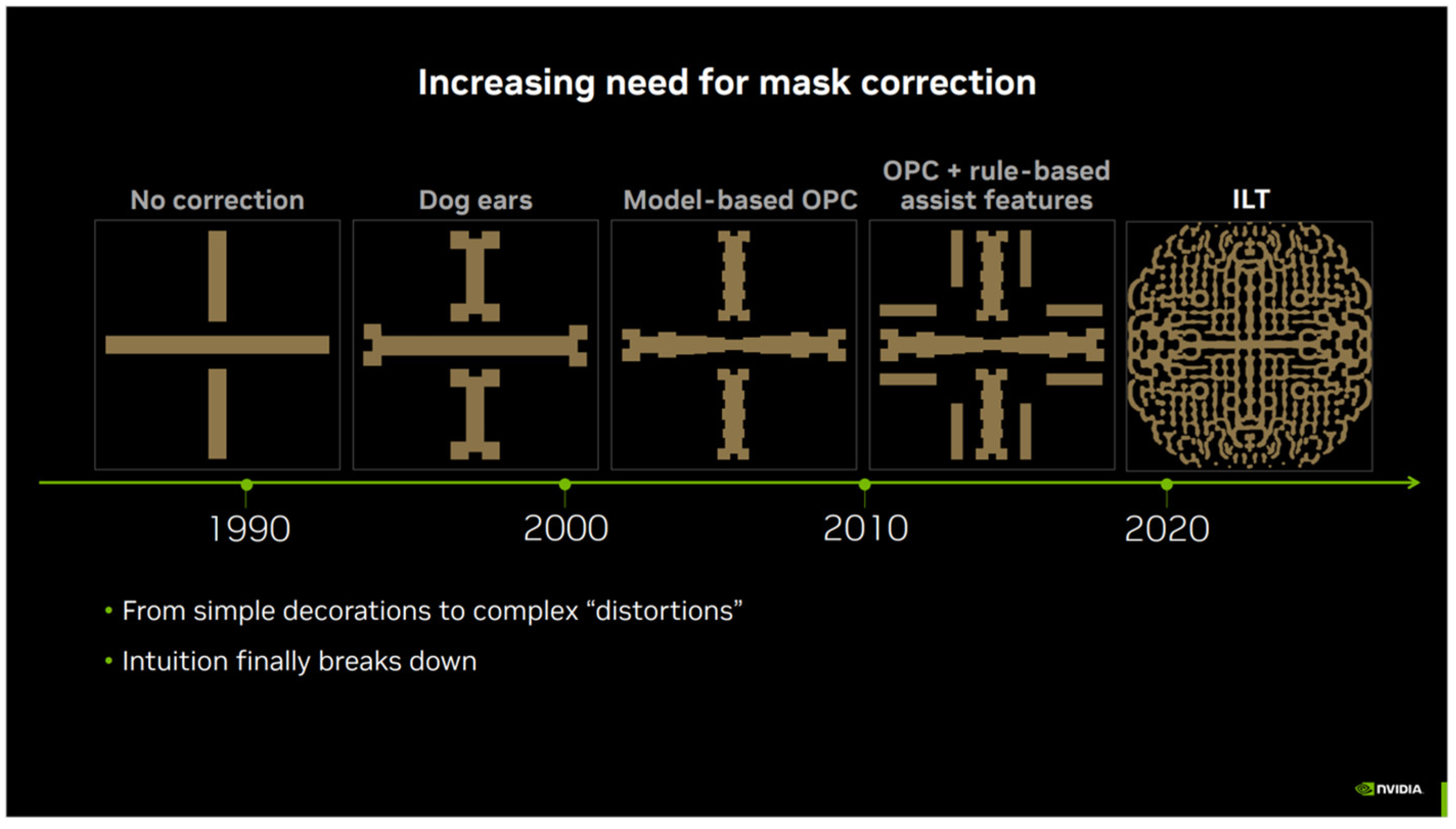
Figure 3.
The general process of ILT [12].
Figure 3.
The general process of ILT [12].
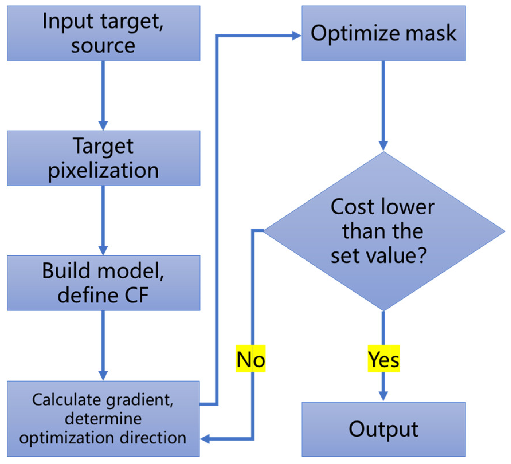
Figure 4.
The process of converting a 2D closed curve into a 3D surface [35].
Figure 4.
The process of converting a 2D closed curve into a 3D surface [35].
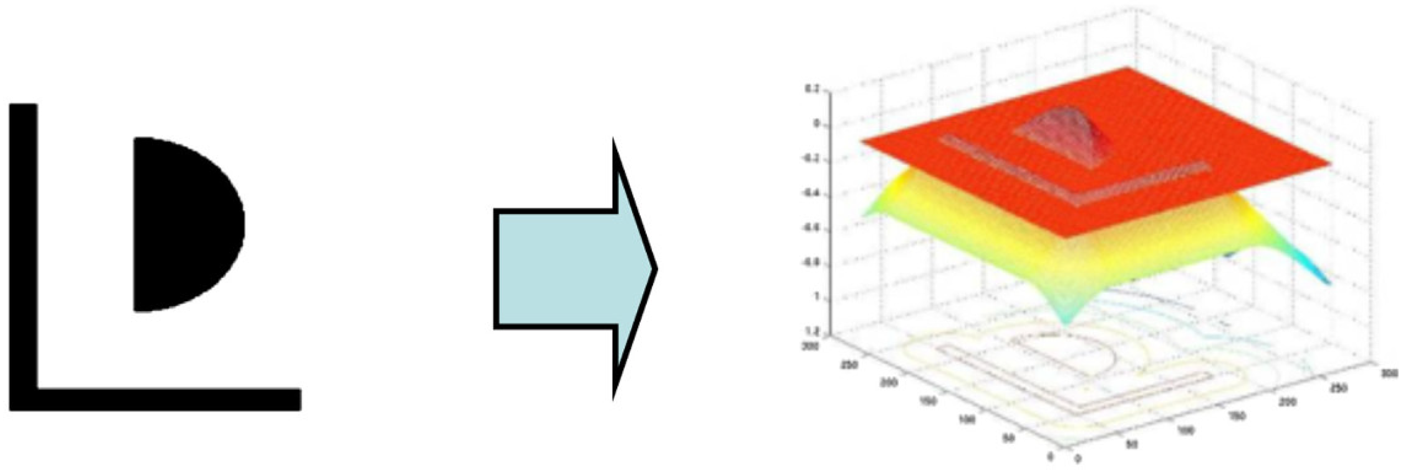
Figure 5.
The schematic diagram of generating SRAF by level-set method [35].
Figure 5.
The schematic diagram of generating SRAF by level-set method [35].
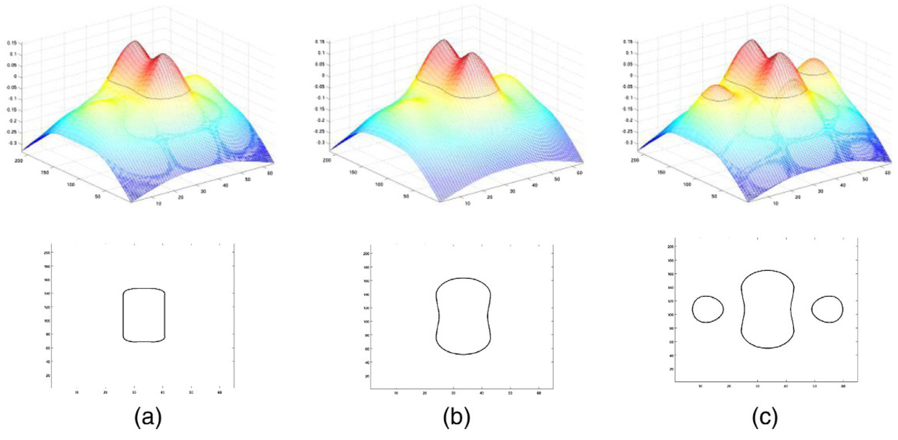
Figure 6.
Pixel optimization flow [36].
Figure 6.
Pixel optimization flow [36].
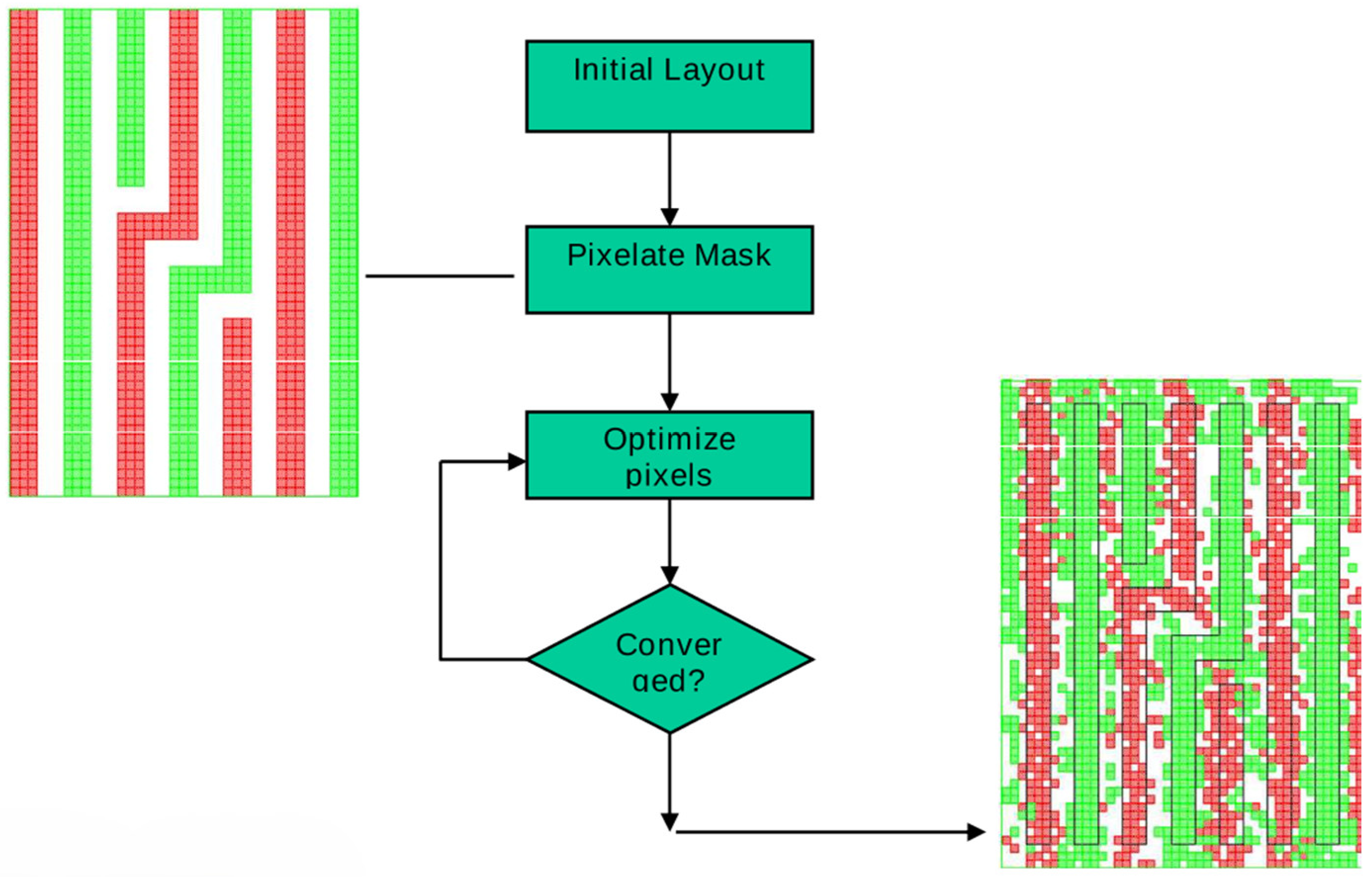
Figure 7.
Process window CD measurements. The highlighted regions are within an acceptable process window [38].
Figure 7.
Process window CD measurements. The highlighted regions are within an acceptable process window [38].
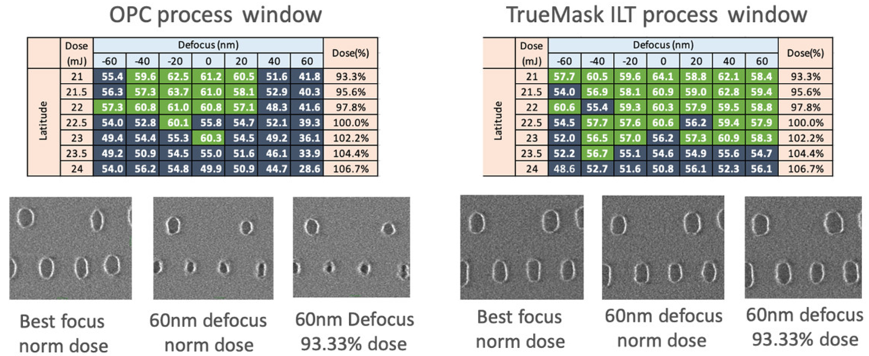
Figure 8.
Machine learning generates full-chip SRAF [44].
Figure 8.
Machine learning generates full-chip SRAF [44].
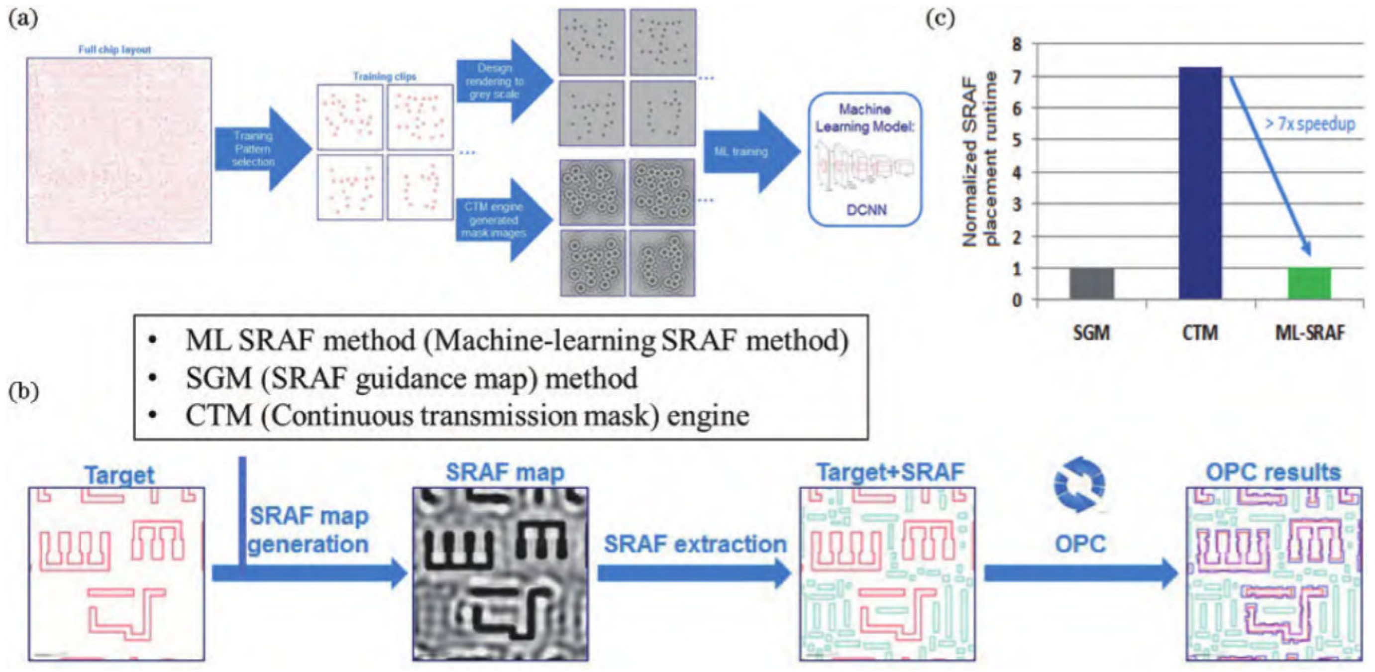
Figure 9.
Annual number of publications on the topic of “inverse lithography technology”.
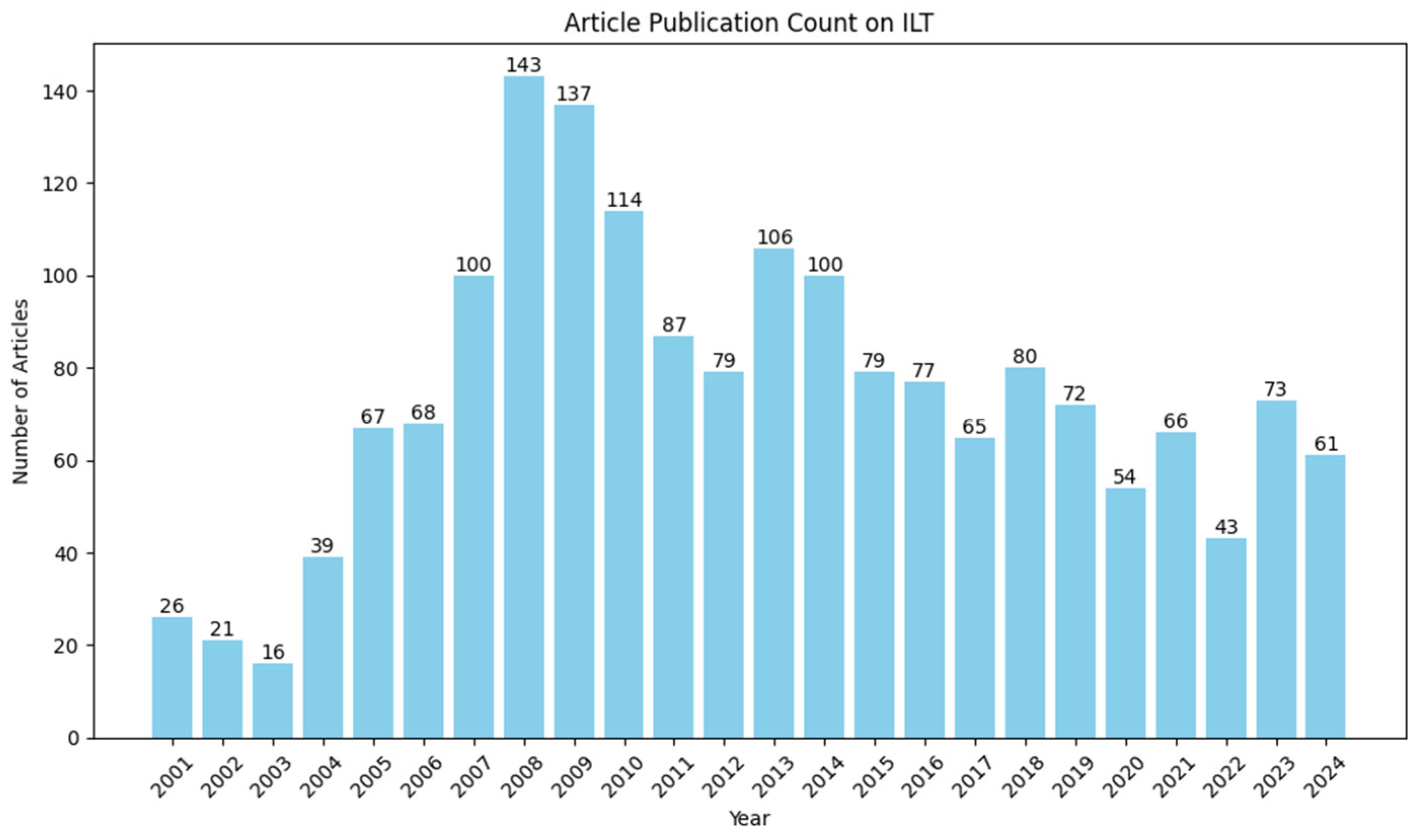
Figure 10.
Annual number of publications in the paper “Inverse lithography technology: 30 years from concept to practical, full-chip reality”.
Figure 10.
Annual number of publications in the paper “Inverse lithography technology: 30 years from concept to practical, full-chip reality”.
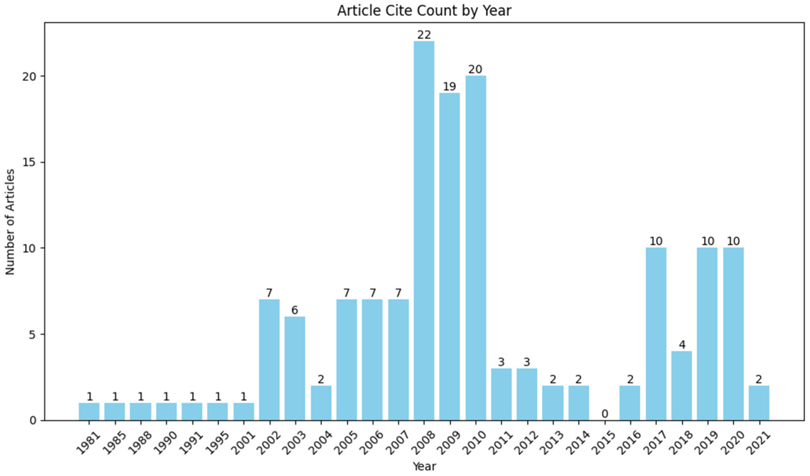
Figure 11.
A revolutionary improvement from VSB to MBMW has been achieved [84].
Figure 11.
A revolutionary improvement from VSB to MBMW has been achieved [84].
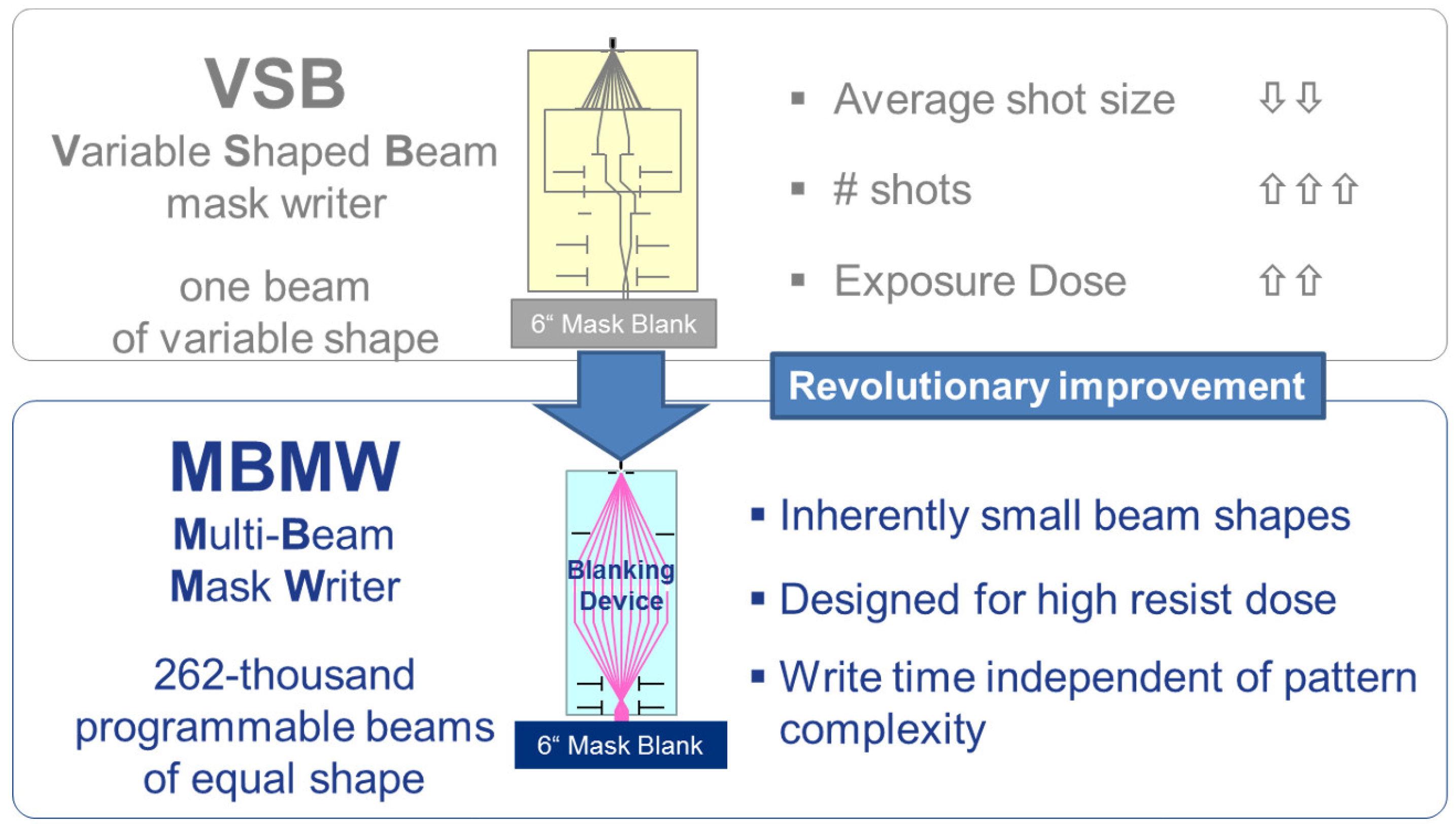
Figure 12.
MBMW-101 ALPHA Tool [84].
Figure 12.
MBMW-101 ALPHA Tool [84].
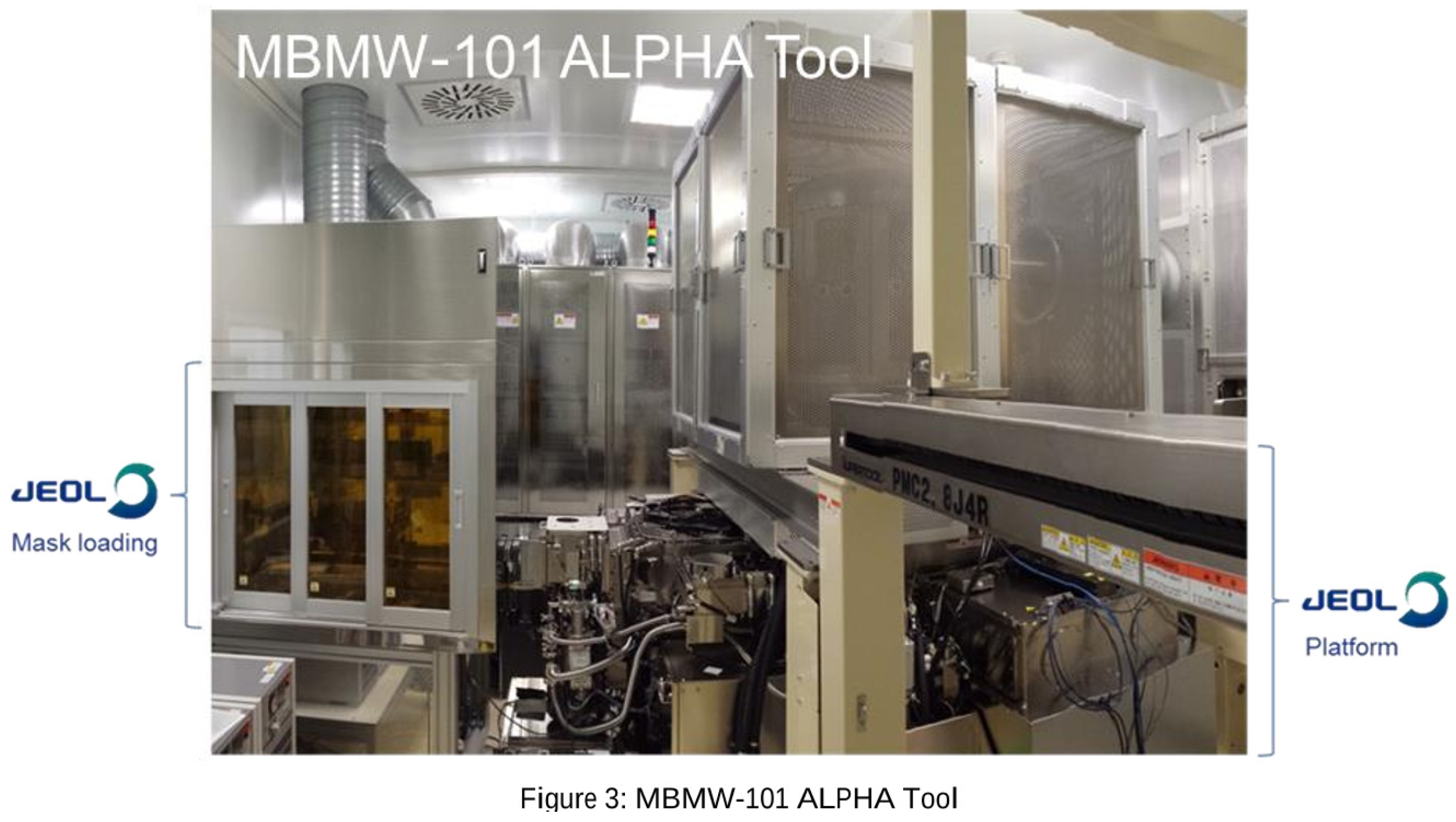
Figure 13.
TrueMask ILT GPU-CPU pairs [38].
Figure 13.
TrueMask ILT GPU-CPU pairs [38].
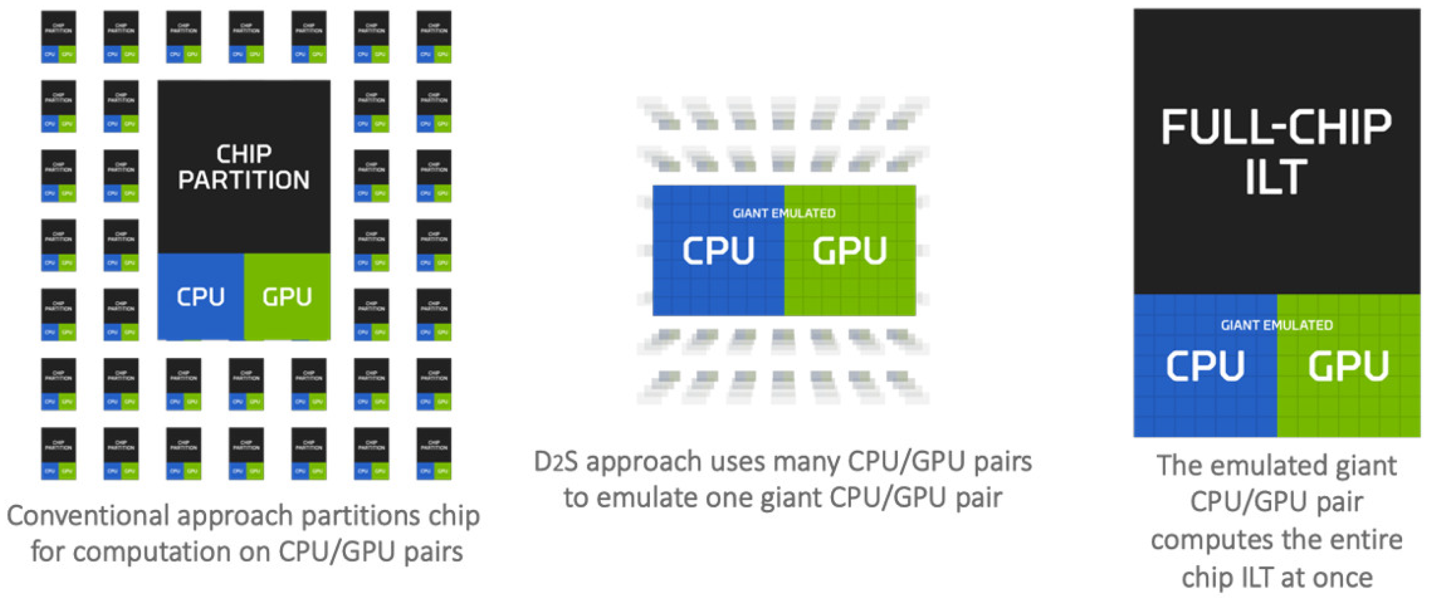
Figure 14.
Process window CD measurements. The highlighted regions are within an acceptable process window [38].
Figure 14.
Process window CD measurements. The highlighted regions are within an acceptable process window [38].
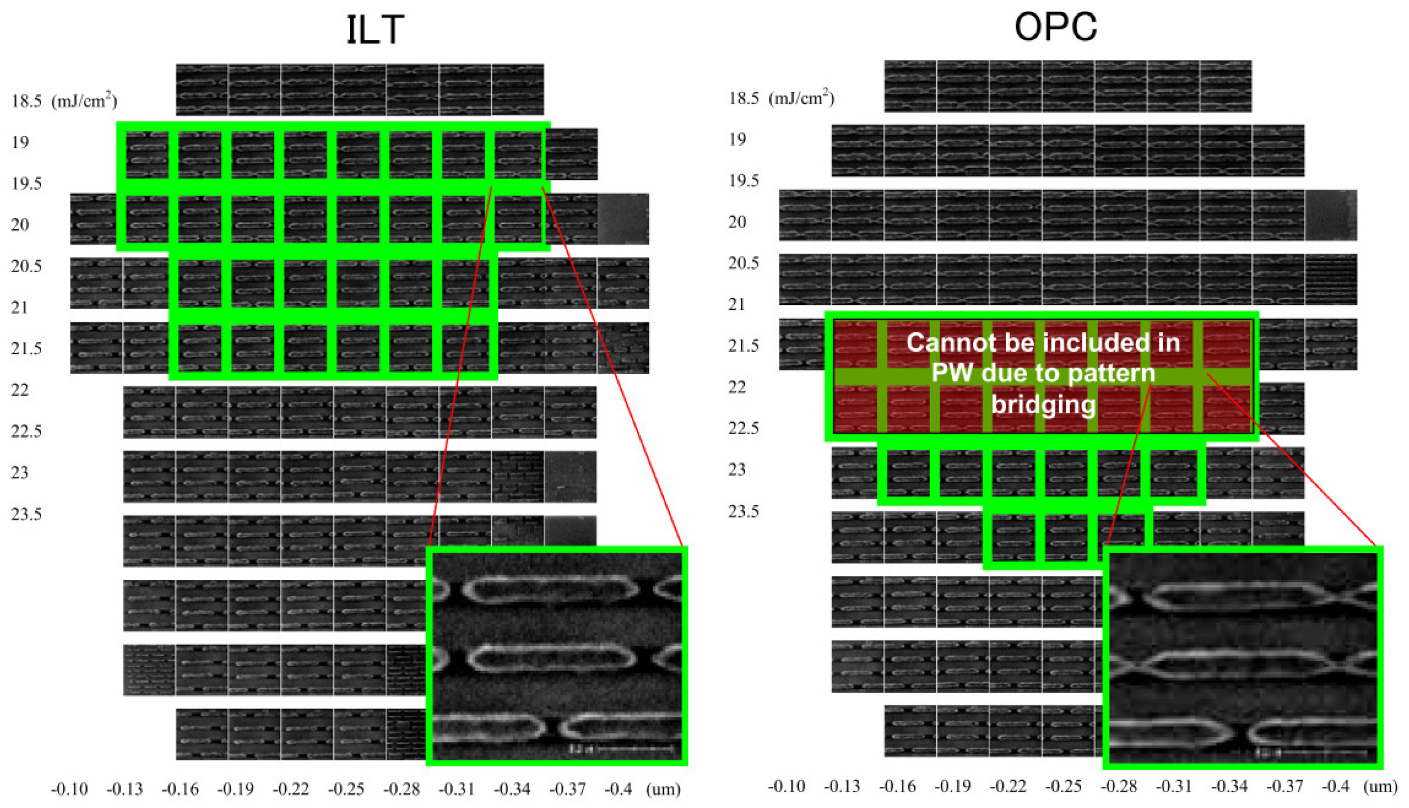
Figure 15.
ILT Performance Is Getting Faster with GPUs [3].
Figure 15.
ILT Performance Is Getting Faster with GPUs [3].
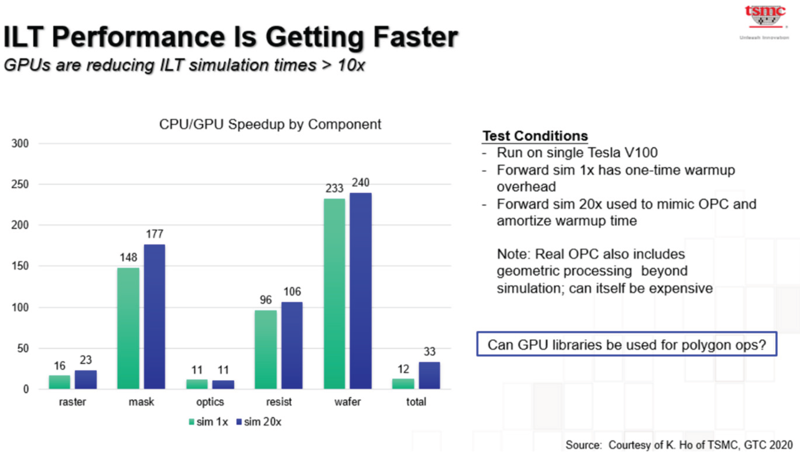
Disclaimer/Publisher’s Note: The statements, opinions and data contained in all publications are solely those of the individual author(s) and contributor(s) and not of MDPI and/or the editor(s). MDPI and/or the editor(s) disclaim responsibility for any injury to people or property resulting from any ideas, methods, instructions or products referred to in the content. |
© 2025 by the authors. Licensee MDPI, Basel, Switzerland. This article is an open access article distributed under the terms and conditions of the Creative Commons Attribution (CC BY) license (https://creativecommons.org/licenses/by/4.0/).
Copyright: This open access article is published under a Creative Commons CC BY 4.0 license, which permit the free download, distribution, and reuse, provided that the author and preprint are cited in any reuse.


