Submitted:
13 August 2025
Posted:
14 August 2025
You are already at the latest version
Abstract
Ferroelectric oxides, such as Pb(Zr,Ti)O3 (PZT), have been shown to maintain stable ferroelectricity even in ultrathin film configurations. However, achieving controllable modulation of microstructure and physical responses in these ultrathin films remains challenging, limiting their potential applications in modern nanoelectronics and optoelectronics. Here, we propose a single-pulse femtosecond (fs) laser micromachining technique for high-precision engineering of microstructure and ferroelectric/piezoelectric responses in ultrathin PZT films. The results show that various microstructures can be selectively fabricated through precise control of fs laser fluence. Specifically, nano-concave arrays are formed via low-fluence laser irradiation, which is mainly attributed to the fs laser peening effect. In contrast, nano-volcano (nano-cave) structures are generated when the laser fluence is close to or reaches the ablation threshold. Additionally, applying an fs laser pulse with fluence exceeding a critical threshold enables the formation of nano-cave structures with controlled depth and width in PZT/Pt/SiO2 multilayers. Piezoresponse force microscopy measurements demonstrate that the laser peening process significantly enhances the piezoelectric response while exerting minimal influence on the coercive field of PZT thin films. This improvement is attributed to polar structure reconstruction induced by lattice tensile deformation resulting from the laser peening effect. Our study not only offers an effective strategy for microstructure and property engineering in ferroelectric materials at the nanoscale, but also provides new insights into the underlying mechanism of ultrafast laser processing in ferroelectric thin films.
Keywords:
ferroelectric oxide thin films
; single-pulse femtosecond laser
; microstructural engineering
; fs laser peening
; ferroelectric and piezoelectric responses
Introduction
In recent years, the rapid development of intelligent electronics and internet of things technologies has driven an increasingly urgent demand for high-speed and highly reliable memory devices in embedded systems [1,2]. Ferroelectric random access memory (FeRAM), with its non-volatility, low power consumption, and high read/write speed, has emerged as a promising candidate for next-generation memory applications [3,4]. Among FeRAM configurations, ferroelectric oxides [e.g., Pb(Zr,Ti)O3] and their heterostructures have attracted extensive attention due to their high storage density and tunable interfacial coupling effects [5,6,7]. Moreover, it has been shown that ferroelectric oxides can maintain stable ferroelectricity in ultrathin films even down to one nanometer limit [8]. However, the modulation of microstructural and physical properties in ultrathin ferroelectric oxide films remains not fully explored [9,10,11,12], thereby limiting their potential applications in modern nanoelectronics and optoelectronics [13,14,15].
Femtosecond (fs) lasers, as ultrafast and ultra-intense energy carriers, enable high-precision micro-processing and induce phase changes in target materials within extremely short timescales [16,17,18,19]. Compared to longer laser pulses, fs lasers offer key advantage of minimizing the heat-affected zone, which facilities precise control of the microstructure features [20,21,22,23]. Previous studies have demonstrated that focused fs laser beams with fluence close to the ablation threshold can directly create crater, nano-bumps, jet-like structures, and complete material removal in various thin films [24,25,26,27]. Additionally, fs lasers have been widely applied in the fabrication of novel functional materials and the modulation of device performance [16,28,29]. However, the dynamic microstructural and physical responses of ferroelectric oxide ultrathin films under fs laser pulse irradiation remain largely unexplored.
In this work, we report on the high-precision engineering of microstructure and ferroelectric/piezoelectric responses in Pb(Zr,Ti)O3 (PZT) ultrathin films using single-pulse fs laser micromachining technique. Optical microscopy and atomic force microscopy (AFM) characterizations reveal a progressive evolution of microstructures with increasing fs laser pulse fluence. When employing laser fluence below 0.5 nJ, nano-concave arrays are achieved in PZT thin films, which are attributed to fs laser peening effect. As the laser fluence increases to 1 nJ, nano-volcano structures emerge, while ablation occurs at a fluence of approximately 2 nJ. Additionally, single-point fs laser irradiation with fluence exceeding 2 nJ enables the formation of nano-cave structures with controlled depth and width in PZT/Pt/SiO2 multilayers, which results from a combination of fs laser ablation and melting effects. Piezoresponse force microscopy (PFM) measurements demonstrate that the laser peening process significantly enhances the piezoelectric response while exerting minimal influence on the coercive field of PZT ultrathin films. The enhanced piezoelectric response originates from fs laser peening-induced atomic lattice deformation and residual stress field, where residual stress promotes efficient alignment of polar domains and enhancement of piezoelectric coefficient. Our study provides an ultrafast, non-contact laser-based approach for precisely modulating the microstructure and physical properties of ferroelectric ultrathin films, offering new pathways for the development of next-generation high-performance non-volatile memory devices.
Results and Discussion
For the ferroelectric oxide layer, we worked with 50-nm-thick PZT thin film deposited on SiO2(285 nm)/Si substrate (Figure S1), with a 150-nm-thick Pt buffer layer severing as the bottom electrode. The PZT thin films were grown by magnetron sputtering, followed by rapid thermal annealing (see Method) to improve the crystallinity of the perovskite phase. To analyze the intrinsic ferroelectric characteristics of PZT thin films, we performed PFM studies (see Method). Figure 1a displays the switching hysteresis of phase and amplitude responses taken on the as-grown PZT thin films, where the coercive voltages for the polarization down (Pdn) and polarization up (Pup) states are 0.78 V and -0.93 V, respectively. Figure 1b shows the AFM image of the PZT thin film deposited on Pt/SiO2/Si substrate, which exhibits relatively smooth surface with a root mean square of ~1.4 nm. Figure 1c and 1d represent the PFM amplitude and phase images of the box-in-box domain structure written on 50 nm PZT film by applying a DC bias voltage of ±10 V to the AFM tip, which exhibits uniform Pdn and Pup domain pattern. The above PFM characterizations confirm the exceptional polarization controllability and nanoscale domain engineering capability in the as-grown PZT ultrathin films.
Various laser-material interaction dynamics are considered to exist between single-pulse fs laser irradiation and PZT ultrathin film (Figure 1e). As shown in Figure 1e (left panel), during low-fluence single-pulse fs laser irradiation, high-energy photons induce nonlinear ionization effect that liberates surface electrons from atomic confinement, resulting in the generation of transient high-density plasma. The rapid expansion of this plasma produces ultrahigh-pressure shock waves that significantly exceed the material’s yield strength, thereby inducing plastic deformation in the PZT layer [30,31]. This shock peening effect is anticipated to enable surface modification of PZT thin film at nanoscale spatial resolution, such as the formation of nano-concave structures. When the singe-pulse fs laser fluence approaches the critical threshold, ablation begins to occur, leading to the formation of nano-volcano (nano-cave) structures in the PZT thin film (Figure 1e (middle panel)). Further increasing fs laser fluence beyond this threshold simultaneously triggers ablation in the PZT layer and melting in the Pt layer (Figure 1e, (right panel)), resulting in the formation of more complex nano-concave structures [32,33].
Based on the above assumption, we next employ a single-pulse fs laser micromachining technique for high-precision nano-engineering of PZT/Pt/SiO2 multilayers, through which various nanostructures could be controllably fabricated. Figure 2a schematically illustrates the fabrication of nanostructure arrays in PZT thin films via single fs laser pulse scan. A fs laser beam with the wavelength of 1030 nm was focused onto the surfaces of the PZT thin films, with a high-precision electrically controlled sample stage enabling two-dimensional (2D) scanning for nanostructure array fabrication. The spacing of nanostructure array can be well controlled by adjusting the laser scanning speed. Figure 2b,c show the optical and AFM images of PZT thin films by single fs laser pulse irradiation at different laser fluences (ranging from 0.2 nJ to 1 nJ) with a scanning pitch of approximately 0.96 μm. The white dashed circles represent fs laser pulse irradiation sites, and a distinct fluence-dependent nanostructure evolution is observed. When employing a weak laser fluence of 0.2 nJ, no apparent structural change is optically resolvable (Figure 2b1). However, the corresponding AFM topography and cross-sectional profile analyses reveal periodic height modulation (Figure 2c1), indicative of weak shock peening effect induced by single-pulse fs laser irradiation [34]. The laser shock peening effect has been predominantly applied to enhance fatigue resistance in bulk and metallic materials such as stainless steel [35]. Here, we for the first time realize fs laser peening-induced nanostructure engineering in ferroelectric oxide ultrathin films.
Upon increasing the single-pulse fs laser fluence to 0.3 nJ, discernible surface modification emerges optically (Figure 2b2), meanwhile AFM topography shows that the depth of depression is intensifying (Figure 2c2), confirming the enhancement of laser peening effect. Remarkably, under 0.4 - 0.5 nJ single-pulse fs laser irradiation conditions, the shock peening effect becomes more pronounced (Figure 2b3,b4), which leads to the formation of uniform and distinct nano-concave arrays in PZT thin films (Figure 2c3,c4). In contrast, under 1 nJ single-pulse fs laser irradiation, nano-volcano arrays are formed in the PZT thin film (Figure 2b5,c5), which can be attributed to thermomechanical coupling effect involving radial migration and resolidification of molten material [36]. Hence, 1 nJ is the critical transition threshold of PZT thin film between the shock peening-dominated regime (< 1 nJ) and ablation-initialized regime (≥ 1 nJ).
Figure 2d quantitatively analyzes the dependence of nanostructure (nano-concave or nano-volcano) depth on fs laser fluence. Here, the depth is defined as the height difference for the modified zone between adjacent peak level and valley level. In the weak fluence region (0.2 - 0.5 nJ), the depth of nanostructure (nano-concaves) linearly increases, reflecting highly fluence-dependent non-thermal shock peening effect (left inset). With a relatively higher fluence (~1 nJ), nano-volcano structures are formed and show significant depth fluctuation, suggesting that thermal ablation begins to occur beyond this threshold (right inset). The established fluence-dependent nanostructure evolution rules provide critical guidance for single-pulse fs laser high-precision nano-engineering in ferroelectric ultrathin films.
Next, we explore the effect of single-pulse fs laser irradiation on the ferroelectric and piezoelectric responses in PZT ultrathin films using PFM technique. Figure 3a compares the switching hysteresis of PFM phase response taken on PZT nanostructure arrays fabricated with fs laser peening at different laser fluences, where similar phase hysteresis curves are detected. Figure 3c quantitatively analyzes the dependence of coercive voltage (VC) extracted from Figure 3a on fs laser fluence. It is clear that VC remains stable (~0.5 ± 0.1 V) across a wide laser fluence range of 0.2 nJ to 1.0 nJ. This indicates that the ferroelectric polarization switching energy barrier does not alter. Thus, we can conclude that the fs laser peening process exerts minimal influence on the ferroelectric properties of PZT ultrathin films. Figure 3b compares the switching hysteresis of PFM amplitude response taken on the same sample in Figure 3a at different laser fluences. The dependence of maximum amplitude extracted from Figure 3b on fs laser fluence is shown in Figure 3d. It is found that, with increasing the laser fluence, the amplitude signal continuously increases, revealing significant enhancement of piezoelectric performance in PZT thin films. This improvement may originate from fs laser peening-induced atomic structural deformation and residual stress field (Figure 3d inset) [29], which promotes efficient alignment of polar domains and enhancement of piezoelectric coefficient.
To further confirm the effect of laser peening on the ferroelectric/piezoelectric responses in PZT thin films, we performed ferroelectric domain pattern writing in both laser peening and no laser peening regions. Figure 3e shows the optical image of a PZT thin film partially processed with fs laser peening at a fluence of 0.5 nJ, where the upper half corresponds to no laser peening region, and the lower half represents the laser-peening processed region. Figure 3f,g show the PFM amplitude and phase images of the square domain structure written on the same region as in Figure 3e by applying a bias voltage of ±10 V to the AFM tip. It is clear that both laser-peened and un-peened regions exhibit uniform Pdn and Pup domain pattern, thus confirming that fs laser peening does not suppress, but rather enhances, the ferroelectric/piezoelectric responses of PZT thin films. The established fs laser fluence and property correlation offers new pathway for developing high-performance ferroelectric non-volatile memory devices.
The aforementioned discussions are mainly focused on the dynamic responses of PZT ultrathin films under fs laser irradiation at relatively low-fluence levels (≤ 1 nJ), where complete ablation does not occur. In the following section, we investigate the impact of fs laser ablation on the microstructural characteristics of PZT thin films. It is predicted that complete ablation would occur at a fluence of 2 nJ, through which nano-cave structures could be obtained (Figure 1e (middle panel)).
The scanning pitch plays an important role in the nanostructure array fabrication. In Figure 4a–d, we designed nanostructure arrays to be formed in PZT thin film by single-pulse fs laser scan at different step sizes (ranging from 0.96 to 0.48 μm). Figure 4e and 4i show the optical and AFM images of the nanostructure arrays fabricated in PZT thin film with a fluence of 2 nJ at step size of 0.96 μm, confirming achievement of uniform and periodic nano-cave structures. The cross-sectional height profiles reveal that the average depth of nano-cave structure is 50 nm, which is in good agreement with the thickness of PZT thin film. It is demonstrated that single-pulse fs laser irradiation possess capability for atomic-level, selective removal of ultrathin films in the (PZT/Pt/SiO2) multilayer system.
When the step size is reduced to 0.8 μm (Figure 4b), as expected, nanoscale rhombic arrays are formed in the PZT layer, as evidenced by optical microscopy and AFM topography characterizations (Figure 4f,j). By reducing the step size to 0.64 μm (Figure 4c), we achieve the complete removal of the PZT layer (Figure 4g and 4k), without causing damage to the underlying Pt layer. This outcome can be attributed to the first-order overlap effect, which results in continuous spatial superposition of the fs laser beam. Concurrently, the accumulated equivalent pulse count within the overlapping region reaches approximately 2 pulses per unit area (Figure 4c). This value is sufficient to meet the ablation threshold of the PZT layer while remaining below the damage threshold of the Pt layer. When the step size is further reduced to 0.48 μm (Figure. 4d), a secondary overlap effect occurs, increasing the pulse density to approximately 3 pulses per unit area. Under this condition, a remarkable increase in surface roughness is observed in the fs laser-scanned region (Figure 4h,l), indicating that the Pt layer has been damaged. The aforementioned discovery provides a universally applicable fs laser-based methodology for high-precision “etching” of ferroelectric ultrathin films, demonstrating substantial potential for the nano-fabrication of integrated ferroelectric memory devices and piezoelectric micro-electromechanical systems.
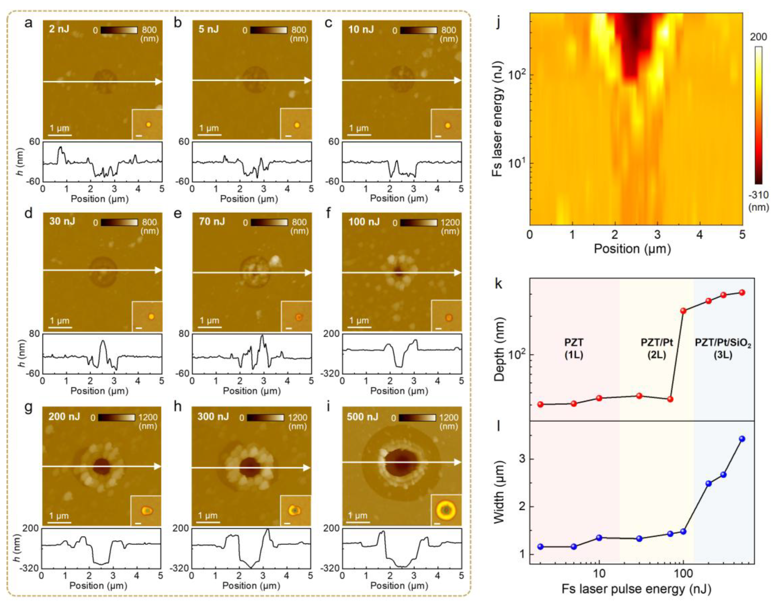
Finally, we investigate the controllable modulation of microstructures in PZT-based heterostructures under single-point fs laser irradiation. Figure 5a–i compare the AFM topographies of nanostructures fabricated on PZT/Pt/SiO2 multilayers using a single fs laser pulse with fluence ranging from 2 nJ to 500 nJ. The insets in Figure 5a–i show the corresponding optical images. In the relatively low fluence range (2 nJ to 10 nJ, Figure 5a–c), nano-cave structures are formed due to the laser ablation effect. These structures exhibit nearly consistent depth (~50 nm), while their diameter increases progressively with increasing fluence. At this stage, the applied fluence exceeds the ablation threshold of the PZT layer but remains below the damage threshold of the Pt/SiO2 substrate, enabling spatially selective removal of the PZT layer. In the medium-fluence range (30 nJ to 100 nJ), both AFM imaging and optical contrast (Figure 5d–f) indicate that fs laser melting and ablation occur in the Pt layer. Specifically, at a fluence of 30 nJ, a molten protrusion appears at the center of the laser-irradiated region (Figure 5d). This phenomenon is attributed to the Gaussian-type intensity profile of the laser beam [37], where only the central region receives sufficient fluence to exceed the melting point of the Pt layer. When the fluence increase to 70-100 nJ (Figure 5e,f), both ablation and melting processes occur within the Pt layer, resulting in the formation of nano-cavities at the central region. Concurrently, molten-solidified ring structures are observed in the peripheral area, which is attributed to the radial gradient of the laser energy distribution. In the high fluence regime (200 nJ to 500 nJ), fs laser melting and ablation occur across the entire PZT/Pt/SiO2 multilayer. At 200 nJ, the initial modification of SiO₂ layer is observed. Upon increasing fluence to 300 nJ, a four-tier annular structure forms, consisting of an outermost PZT ablation zone, an intermediate Pt molten ring, an inner Pt ablation region, and a central SiO₂ etching pit. At 500 nJ, this hierarchical architecture stabilizes and expands in both width and depth.
Figure 5j displays the 3D height profiles of nano-cave structures fabricated in PZT/Pt/SiO2 multilayer at different fs laser pulse fluences, offering a more intuitive understanding of the interaction between the fs laser and the multilayer system. In the lower energy regime, ablation of PZT layer dominates the process, with the ablation diameter expanding as the laser fluence increases. When the fluence reaches a critical threshold, both the interaction depth and diameter increase abruptly. Figure 5k and 5i quantitively analyze the dependence of nano-cave structure depth and width on fs laser pulse fluence, respectively. It can be observed that below 100 nJ, both depth and width exhibit gradual increases, whereas above 100 nJ, exponential growth is evident. This indicates that the penetration depth and interaction area in the multilayer system do not scale linearly with fs laser fluence. By precisely adjusting the fs laser fluence, nano-cave structures with controlled depth and width can be fabricated in PZT/Pt/SiO2 multilayers.
Conclusions
In summary, we have realized giant modulation of microstructure, as well as ferroelectric and piezoelectric responses, in ultrathin (~50 nm) PZT films through single-pulse fs laser irradiation. By precisely controlling the fs laser fluence and scanning pitch, various nanostructures arrays, including nano-concave array, nano-volcano array, and nano-cave array, can be selectively fabricated within the PZT thin layer. It is found that the fs laser peening (ablation) effect primarily governs the formation of nano-concaves (nano-caves) in the PZT thin film, while a combination of fs laser ablation and melting effects enable the controlled fabrication of complex nano-cavities with tunable depth and width in the PZT/Pt/SiO₂ multilayers. PFM investigations reveal that laser peening significantly enhances the piezoelectric performance while exerting minimal influence on the ferroelectric response of the PZT thin films. This enhancement is attributed to atomic structural deformation and residual stress field induced by fs laser peening. These findings present an efficient ultrafast laser-based strategy for precisely modulating the microstructure and functional properties of ferroelectric oxide thin films, opening new avenues for the development of high-performance non-volatile memory devices.
Methods
Preparation of PZT thin films. Ferroelectric PZT thin films were deposited by radio-frequency (RF) sputtering method on the Pt/Ti-coated SiO2/Si substrate, followed by the rapid thermal annealing. First, Pt/Ti/SiO2/Si substrates were prepared by sputtering 20 nm Ti and then 150 nm Pt onto SiO2(285 nm)/Si substrate. Second, PZT thin films were deposited using RF sputtering with PbZr0.48Ti0.52O3 target. The deposition was carried out at 200°C, with a gas flow of 70 sccm Ar and 0.5 sccm O2, under a working pressure of 1 Pa. The power of PbZr0.48Ti0.52O3 target was fixed at 67 W. The thickness of PZT film was controlled through the sputtering time. Third, the rapid thermal annealing treatment was performed at 650°C for 8 min in an O2 environment.
AFM and PFM measurements. The morphologies and thicknesses of the PZT thin films were measured using an AFM system (MFP-3D Origin, Oxford) with an AFM tip (Micromesh HQ:NSC14, k = 5) working at AC mode. PFM measurements were carried out using the same AFM system with Pt-coated AFM tip (Micromesh HQ:NSC18, k = 2.8) at DART mode. For domain writing, a DC bias of ±10 V was applied to AFM tip and the PZT thin films were grounded. For PFM imaging, a small AC voltage was applied to AFM tip.
Fs laser processing. Fs laser processing was conducted using a laser system with a wavelength of 1030 nm and a pulse duration of 138 fs. The laser output was linearly polarized, with its power controlled using a half-wave plate and a Glan prism. To enable high-resolution processing, the laser beam was focused onto the sample using an objective lens (100× magnification, working distance: 1 mm, NA = 0.9), achieving a focused spot size of approximately 0.63 μm. The samples were mounted on an electrically controlled three-axis sample stage and processed in ambient air. The system allowed for precise control of scanning speed and trajectory for micromachining applications. The laser parameters, including repetition rate and pulse energy, were optimized based on the material and processing conditions to ensure effective micromachining and patterning results.
Supplementary Materials
The following supporting information can be downloaded at: Preprints.org, Thickness measurement of PZT thin films.
Acknowledgements
This work was supported by the National Natural Science Foundation of China (Grant No. 12274051), the Natural Science Foundation of Liaoning Province (Grant No. 2024-MSBA-06), the Liaoning Province Xingliao Talents Plan Project (Grant No. XLYC2403069), the Chunhui Project Foundation of the Education Department of China (Grant No. HZKY20220423), the Fundamental Research Funds for the Central Universities (Grant Nos. DUT24RC(3)060, DUT22ZK109), and the National Key Research and Development Program of China (Grant No. 2024YFE0213500).
References
- Keshavarzi, A.; Ni, K.; Hoek, W.V.D.; Datta, S.; Raychowdhury, A. FerroElectronics for Edge Intelligence. IEEE Micro 2020, 40, 33–48. [Google Scholar] [CrossRef]
- Chen, C.; Zhou, Y.; Tong, L.; Pang, Y.; Xu, J. Emerging 2D Ferroelectric Devices for In-Sensor and In-Memory Computing. Advanced Materials 2025, 37, 2400332. [Google Scholar] [CrossRef]
- Guo, M.; Jiang, J.; Qian, J.; Liu, C.; Ma, J.; Nan, C.-W.; Shen, Y. Flexible Robust and High-Density FeRAM from Array of Organic Ferroelectric Nano-Lamellae by Self-Assembly. Advanced Science 2019, 6, 1801931. [Google Scholar] [CrossRef]
- Chiu, C.-H.; Huang, C.-W.; Hsieh, Y.-H.; Chen, J.-Y.; Chang, C.-F.; Chu, Y.-H.; Wu, W.-W. In-situ TEM Observation of Multilevel Storage Behavior in Low Power FeRAM Device. Nano Energy 2017, 34, 103–110. [Google Scholar] [CrossRef]
- Zou, D.; Liu, S.; Zhang, C.; Hong, Y.; Zhang, G.; Yang, Z. Flexible and Translucent PZT films Enhanced by the Compositionally Graded Heterostructure for Human Body Monitoring. Nano Energy 2021, 85, 105984. [Google Scholar] [CrossRef]
- Yue, Z.Y.; Zhang, Z.D.; Wang, Z.J. Enhanced Memristor Performance via Coupling Effect of Oxygen Vacancy and Ferroelectric Polarization. Journal of Materials Science & Technology 2024, 171, 139–146. [Google Scholar]
- Chen, X.; Zhang, X.; Koten, M.A.; Chen, H.; Xiao, Z.; Zhang, L.; Shield, J.E.; Dowben, P.A.; Hong, X. Interfacial Charge Engineering in Ferroelectric-Controlled Mott Transistors. Advanced Materials 2017, 29, 1701385. [Google Scholar] [CrossRef]
- Fong, D.D.; Stephenson, G.B.; Streiffer, S.K.; Eastman, J.A.; Auciello, O.; Fuoss, P.H.; Thompson, C. Ferroelectricity in Ultrathin Perovskite Films. Science 2004, 304, 1650–1653. [Google Scholar] [CrossRef]
- Yang, H.-L.; Wang, B.-M.; Zhu, X.-J.; Shang, J.; Chen, B.; Li, R.-W. Modulation of Physical Properties of Oxide Thin Films by Multiple Fields. Chinese Physics B 2016, 25, 067303. [Google Scholar] [CrossRef]
- Jiang, R.-J.; Cao, Y.; Geng, W.-R.; Zhu, M.-X.; Tang, Y.-L.; Zhu, Y.-L.; Wang, Y.; Gong, F.; Liu, S.-Z.; Chen, Y.-T.; Liu, J.; Liu, N.; Wang, J.-H.; Lv, X.-D.; Chen, S.-J.; Ma, X.-L. Atomic Insight into the Successive Antiferroelectric–Ferroelectric Phase Transition in Antiferroelectric Oxides. Nano Letters 2023, 23, 1522–1529. [Google Scholar] [CrossRef]
- Gong, J.; Du, P.; Li, W.; Yuan, G.; Mao, X.; Luo, L. The Enhancement of Photochromism and Luminescence Modulation Properties of Ferroelectric Ceramics via Chemical and Physical Strategies. Laser & Photonics Reviews 2022, 16, 2200170. [Google Scholar] [CrossRef]
- Lee, J.; Song, M.S.; Jang, W.-S.; Byun, J.; Lee, H.; Park, M.H.; Lee, J.; Kim, Y.-M.; Chae, S.C.; Choi, T. Modulating the Ferroelectricity of Hafnium Zirconium Oxide Ultrathin Films via Interface Engineering to Control the Oxygen Vacancy Distribution. Advanced Materials Interfaces 2022, 9, 2101647. [Google Scholar] [CrossRef]
- Li, D.; Huang, X.; Wu, Q.; Zhang, L.; Lu, Y.; Hong, X. Ferroelectric Domain Control of Nonlinear Light Polarization in MoS2 via PbZr0.2Ti0.8O3 Thin Films and Free-Standing Membranes. Advanced Materials 2023, 35, 2208825. [Google Scholar] [CrossRef]
- Li, D.; Huang, X.; Xiao, Z.; Chen, H.; Zhang, L.; Hao, Y.; Song, J.; Shao, D.-F.; Tsymbal, E.Y.; Lu, Y.; Hong, X. Polar Coupling Enabled Nonlinear Optical Filtering at MoS2/Ferroelectric Heterointerfaces. Nature Communications 2020, 11, 1422. [Google Scholar] [CrossRef]
- Sun, D.; Zhang, Y.; Wang, D.; Song, W.; Liu, X.; Pang, J.; Geng, D.; Sang, Y.; Liu, H. Microstructure and domain engineering of Lithium Niobate Crystal Films for Integrated Photonic Applications. Light: Science & Applications 2020, 9, 197. [Google Scholar] [CrossRef]
- Wang, M.; Li, D.; Liu, K.; Guo, Q.; Wang, S.; Li, X. Nonlinear Optical Imaging, Precise Layer Thinning, and Phase Engineering in MoTe2 with Femtosecond Laser. ACS Nano 2020, 14, 11169–11177. [Google Scholar] [CrossRef] [PubMed]
- Guo, J.; Zhang, L.; Zhang, M.; Ji, S.; Xiao, Z.; Gao, C.; Liu, F.; Hu, Z.; Zhou, Y.; Fu, X. Femtosecond Laser Manipulation of Multistage Phase Switching in Two-Dimensional In2Se3 Visualized via an In Situ Transmission Electron Microscope. ACS Nano 2025, 19, 13264–13272. [Google Scholar] [CrossRef]
- Fang, R.; Vorobyev, A.; Guo, C. Direct Visualization of the Complete Evolution of Femtosecond Laser-Induced Surface Structural Dynamics of Metals. Light: Science & Applications 2017, 6, e16256–e16256. [Google Scholar]
- Sugioka, K.; Cheng, Y. Ultrafast Lasers—Reliable Tools for Advanced Materials Processing. Light: Science & Applications 2014, 3, e149–e149. [Google Scholar] [CrossRef]
- Li, D.W.; Zhou, Y.S.; Huang, X.; Jiang, L.; Silvain, J.F.; Lu, Y.F. In Situ Imaging and Control of Layer-by-Layer Femtosecond Laser Thinning of Graphene. Nanoscale 2015, 7, 3651–3659. [Google Scholar] [CrossRef]
- Sugioka, K. Progress in Ultrafast Laser Processing and Future Prospects. Nanophotonics 2017, 6, 393–413. [Google Scholar] [CrossRef]
- Hirayama, Y.; Obara, M. Heat-Affected Zone and Ablation Rate of Copper Ablated with Femtosecond Laser. Journal of Applied Physics 2005, 97. [Google Scholar] [CrossRef]
- Chichkov, B.N.; Momma, C.; Nolte, S.; von Alvensleben, F.; Tünnermann, A. Femtosecond, Picosecond and Nanosecond Laser Ablation of Solids. Applied Physics A 1996, 63, 109–115. [Google Scholar] [CrossRef]
- Korte, F.; Koch, J.; Chichkov, B.N. Formation of Microbumps and Nanojets on Gold Targets by Femtosecond Laser Pulses. Applied Physics A 2004, 79, 879–881. [Google Scholar] [CrossRef]
- Koch, J.; Korte, F.; Bauer, T.; Fallnich, C.; Ostendorf, A.; Chichkov, B.N. Nanotexturing of Gold Films by Femtosecond Laser-Induced Melt Dynamics. Applied Physics A 2005, 81, 325–328. [Google Scholar] [CrossRef]
- Nakata, Y.; Miyanaga, N.; Okada, T. Effect of Pulse Width and Fluence of Femtosecond Laser on the Size of Nanobump Array. Applied Surface Science 2007, 253, 6555–6557. [Google Scholar] [CrossRef]
- Hu, D.; Lu, Y.; Cao, Y.; Zhang, Y.; Xu, Y.; Li, W.; Gao, F.; Cai, B.; Guan, B.-O.; Qiu, C.-W.; Li, X. Laser-Splashed Three-Dimensional Plasmonic Nanovolcanoes for Steganography in Angular Anisotropy. ACS Nano 2018, 12, 9233–9239. [Google Scholar] [CrossRef]
- Chen, X.; Liu, D.; Liu, S.; Mazur, L.M.; Liu, X.; Wei, X.; Xu, Z.; Wang, J.; Sheng, Y.; Wei, Z.; Krolikowski, W. Optical Induction and Erasure of Ferroelectric Domains in Tetragonal PMN-38PT Crystals. Advanced Optical Materials 2022, 10, 2102115. [Google Scholar] [CrossRef]
- Fan, L.; Ran, L.; Zhang, S.; Wu, L.; Wang, T.; Zhao, T.; Wang, Y.; Pan, J.; Song, Q.; Lu, J.; Yao, J.; Wu, H. Femtosecond-Laser-Enabled Geometric Microengineering of PZT Films for Boosted Piezoelectric Response and Rainfall Monitoring Demonstration. ACS Applied Materials & Interfaces 2024, 16, 66718–66726. [Google Scholar]
- Yoshida, M.; Nishibata, I.; Matsuda, T.; Ito, Y.; Sugita, N.; Shiro, A.; Shobu, T.; Arakawa, K.; Hirose, A.; Sano, T. Influence of pulse duration on mechanical properties and dislocation density of dry laser peened aluminum alloy using ultrashort pulsed laser-driven shock wave. Journal of Applied Physics 2022, 132, 075101. [Google Scholar] [CrossRef]
- Lian, Y.; Hua, Y.; Sun, J.; Wang, Q.; Chen, Z.; Wang, F.; Zhang, K.; Lin, G.; Yang, Z.; Zhang, Q.; Jiang, L. Martensitic Transformation in Temporally Shaped Femtosecond Laser Shock Peening 304 Steel. Applied Surface Science 2021, 567, 150855. [Google Scholar] [CrossRef]
- Park, M.; Gu, Y.; Mao, X.; Grigoropoulos, C.P.; Zorba, V. Mechanisms of Ultrafast GHz Burst fs Laser Ablation. Science Advances 2023, 9, eadf6397. [Google Scholar] [CrossRef]
- Lamela, J.; Lifante, G.; Han, T.P.J.; Jaque, F.; García-Navarro, A.; Olivares, J.; Agulló-López, F. Morphology of Ablation Craters Generated by fs Laser Pulses in LiNbO3. Applied Surface Science 2009, 255, 3918–3922. [Google Scholar] [CrossRef]
- Ayeb, M.; Frija, M.; Fathallah, R. Laser Peening: A Review of the Factors, Effects, Applications, Comparison with Shot Peening and State-of-the-Art. Metals and Materials International 2024, 30, 259–283. [Google Scholar] [CrossRef]
- Soyama, H. Comparison Between the Improvements Made to the Fatigue Strength of Stainless Steel by Cavitation Peening, Water Jet Peening, Shot Peening and Laser Peening. Journal of Materials Processing Technology 2019, 269, 65–78. [Google Scholar] [CrossRef]
- Chen, Y.; Sun, H.; Lin, G.; Song, S.; Ji, P. Multiphysics Modeling Femtosecond Laser Ablation of Ti6Al4V with Material Transient Properties. Journal of Alloys and Compounds 2024, 1002, 175360. [Google Scholar] [CrossRef]
- Cheng, C.W. Ablation of Copper by a Scanning Gaussian Beam of a Femtosecond Laser Pulse. The International Journal of Advanced Manufacturing Technology 2017, 92, 151–156. [Google Scholar] [CrossRef]
Figure 1.
Characterizations of ferroelectric PZT thin films grown on Pt/SiO2/Si substrate. (a) Switching hysteresis of (top) phase and (bottom) amplitude responses taken on as-grown PZT thin film (~50 nm). (b) AFM topography, PFM (c) amplitude and (d) phase images of square domains written on a PZT thin film. The lower panels in (b-d) show the cross-sectional signal profiles along the white solid lines. The dark and bright regions in (d) represent Pup and Pdown states, respectively. (e) Schematic view showing different interactions between PZT layers and fs laser pulse by varying the laser fluence: (left panel) laser peening effect, (middle panel) laser ablation effect, and (right panel) laser ablation & melting effects.
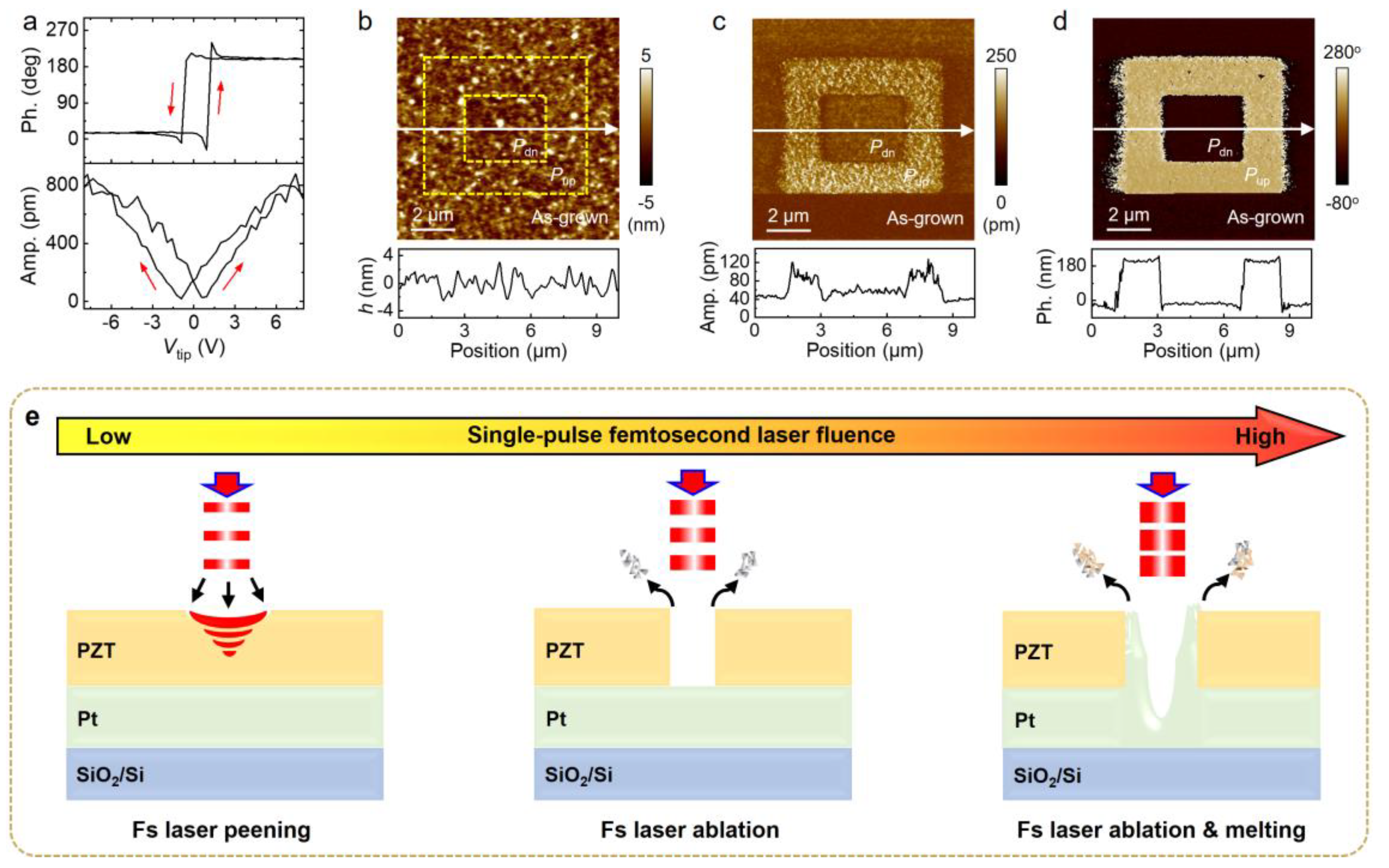
Figure 2.
Fabrication of nano-concave arrays in PZT thin films by fs laser peening. (a) Schematic illustration of microstructure engineering in PZT thin films by single fs laser pulse scan (scanning pitch: ~0.96 μm). (b-c) Optical images (b) and AFM topographies (c) of nanostructures generated on PZT thin film by single fs laser pulse irradiation at different laser fluences (ranging from 0.2 nJ to 1 nJ). The white dashed circles in (b-c) represent fs laser pulse irradiation sites. The lower panels in (c) show the cross-sectional height profiles along the yellow solid lines. The red dotted arrows point to the peening action area (0.2 nJ - 0.5 nJ), while the blue arrows point to the ablation action area (0.5 nJ - 1 nJ). (d) The dependence of nano-concave (or nano-volcano) depth on fs laser pulse fluence. The insets show schematics for nano-concave and nano-volcano formation mechanism via single fs laser pulse.
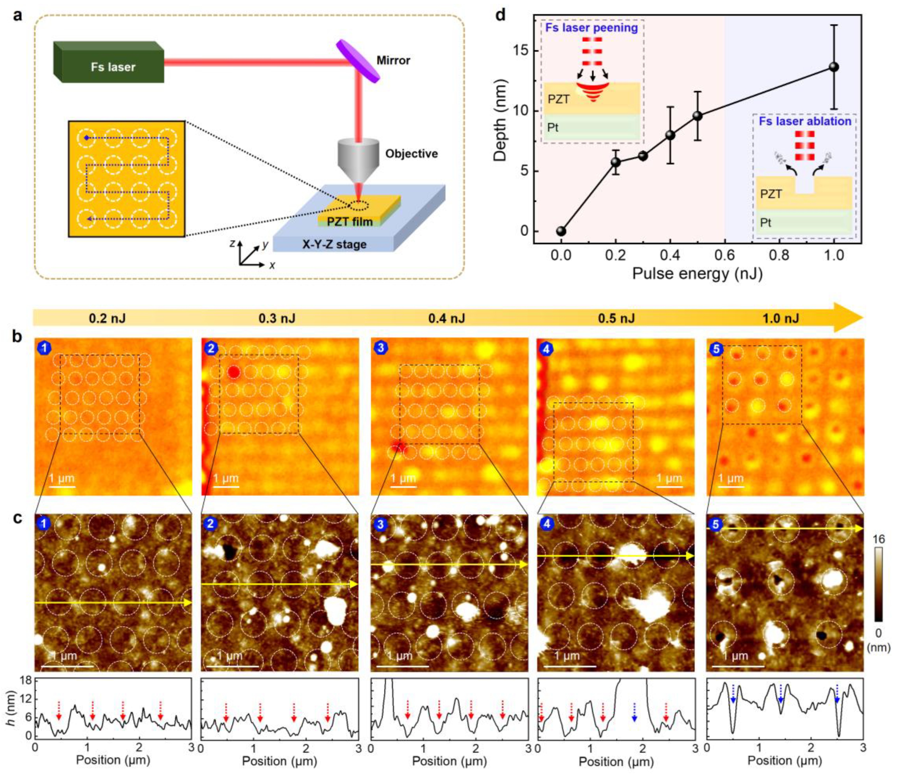
Figure 3.
The effect of fs laser peening on the ferroelectric/piezoelectric properties of PZT thin films. (a-b) Switching hysteresis of PFM (a) phase and (b) amplitude responses taken on PZT nanostructures fabricated with fs laser peening at different laser pulse fluences (from top to bottom: 0.2 nJ, 0.3 nJ, 0.4 nJ, 0.5 nJ, and 1 nJ). (c-d) The dependence of (c) coercive voltage and (d) maximum amplitude extracted from (a-b) on fs laser pulse fluence. Inset in (d): schematic diagrams of the atomic structural evolution in PZT by varying the fs laser pulse fluence. (e) Optical image of a selected region in PZT thin film, with the upper half showing no fs laser peening area and the lower half showing fs laser peening area. The white dotted line marks the boundary of these two areas. (f-g) PFM (f) amplitude and (e) phase images of the same region in (e) with square domains written in both fs laser treated and untreated areas. The lower panels in (f-g) show the cross-sectional signal profiles along the solid lines.
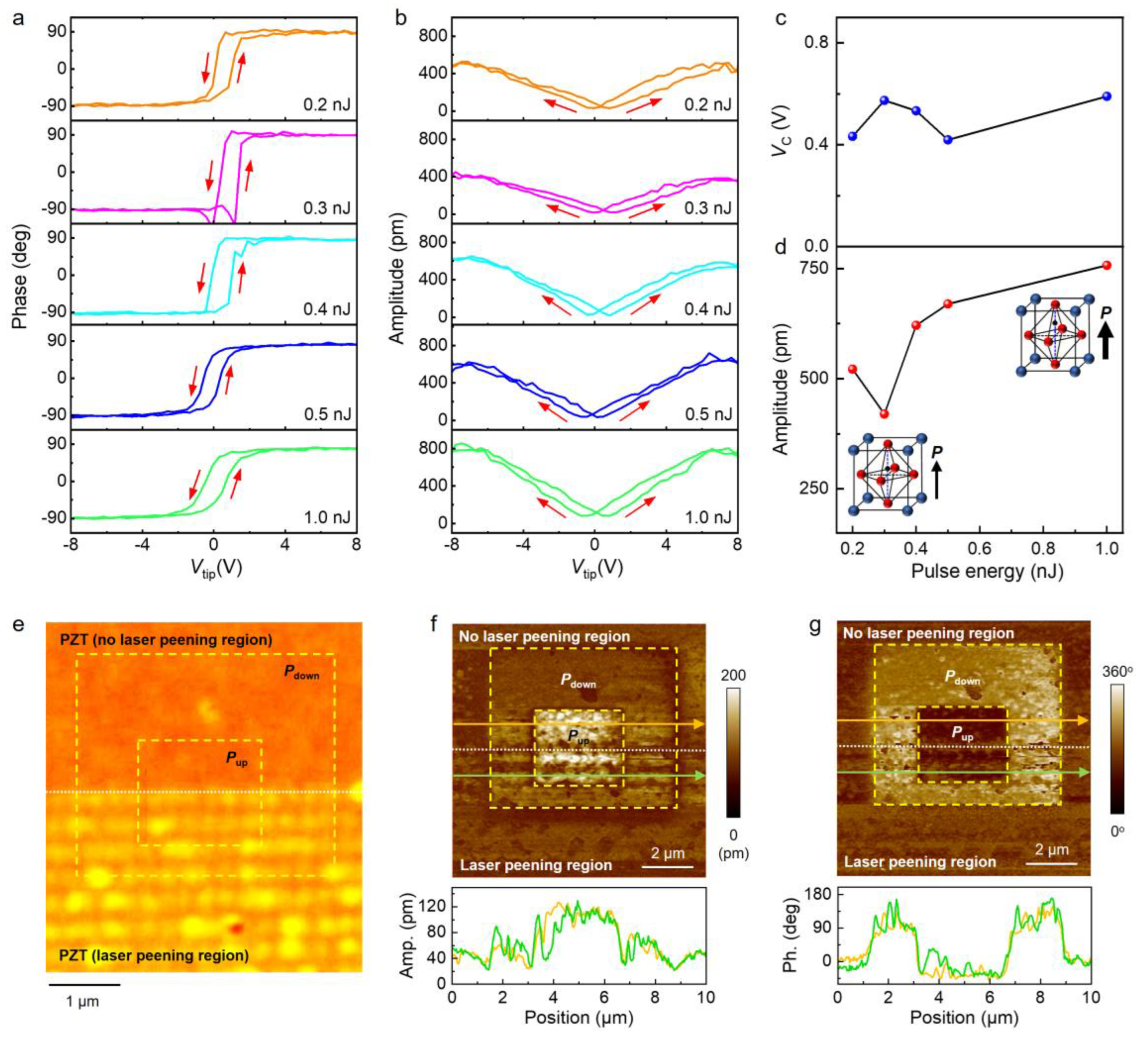
Figure 4.
Fabrication of nano-cave array in PZT thin films by fs laser ablation. (a-d) Schematics of nano-cave array formation in PZT thin film by fs laser scan at different step sizes (from left to right: 0.96 μm, 0.80 μm, 0.64 μm, and 0.48 μm). (e-h) Optical images and (i-l) AFM topographies of nano-cave array fabricated on PZT thin film with a fs laser pulse fluence of 2 nJ at different step sizes: (e,i) 0.96 μm, (f,j) 0.80 μm, (g,k) 0.64 μm, and (h,l) 0.48 μm. The lower panels in (i-l) show the cross-sectional height profiles along the solid lines. The black (blue) and red curves represent the height profiles along the center and edge positions of nano-cave array, respectively.
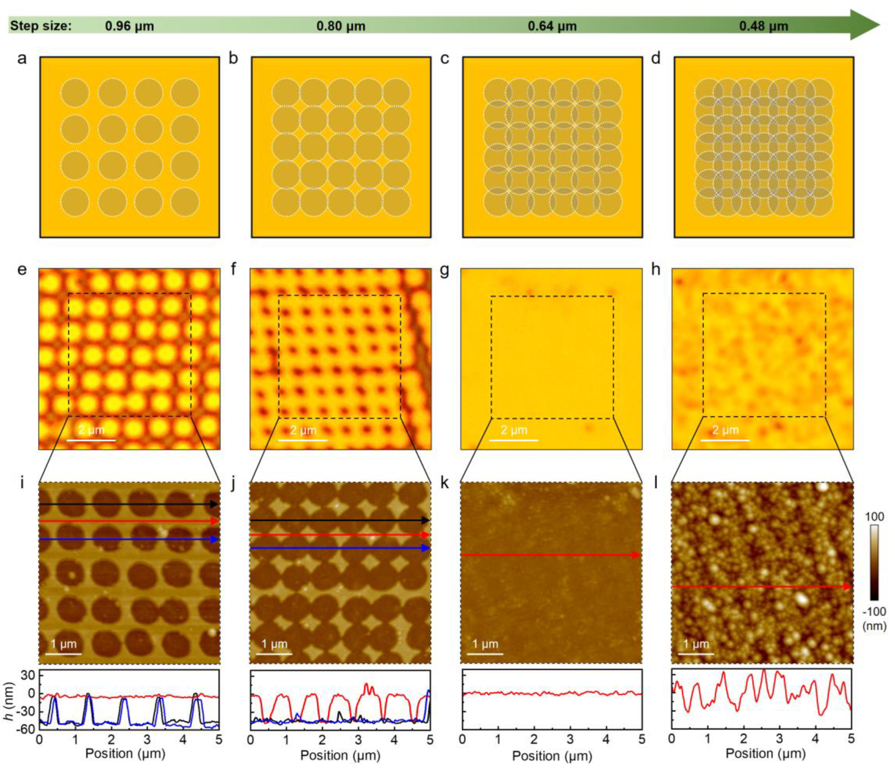
Figure 5.
Nanostructure evolution in PZT/Pt/SiO2 multilayers as laser pulse fluence under single-point fs laser irradiation. (a-i) AFM topographies of nano-cave structures fabricated on PZT/Pt/SiO2 multilayers by single fs lase pulse at a broad laser fluence range of 2 nJ to 500 nJ. Insets: the corresponding optical images. (j) 3D height profiles of nano-cave structures fabricated at different fs laser pulse fluences. (k-l) The dependence of nano-cave structure (k) depth and (l) width on fs laser pulse energy.
Disclaimer/Publisher’s Note: The statements, opinions and data contained in all publications are solely those of the individual author(s) and contributor(s) and not of MDPI and/or the editor(s). MDPI and/or the editor(s) disclaim responsibility for any injury to people or property resulting from any ideas, methods, instructions or products referred to in the content. |
© 2025 by the authors. Licensee MDPI, Basel, Switzerland. This article is an open access article distributed under the terms and conditions of the Creative Commons Attribution (CC BY) license (http://creativecommons.org/licenses/by/4.0/).
Copyright: This open access article is published under a Creative Commons CC BY 4.0 license, which permit the free download, distribution, and reuse, provided that the author and preprint are cited in any reuse.


