
Submitted:
12 August 2025
Posted:
13 August 2025
You are already at the latest version
Abstract
The quantum Hall effect is a paradigmatic example of topological order, characterized by precisely quantized Hall resistance and dissipationless edge transport. These edge states are chiral, propagating unidirectionally along the boundary, and their directionality is determined by the external magnetic field. While chirality is a central feature of the quantum Hall effect, directly probing it remains experimentally nontrivial. In this study, we introduce a simple and effective method to probe the chirality of edge transport using two independently controlled current sources in a Hall bar geometry. The system under investigation is a monolayer epitaxial graphene grown on a silicon carbide substrate, exhibiting robust quantum Hall states. By varying the configurations of the two current sources, we measure terminal voltages and analyze the transport characteristics. Our results demonstrate that the observed behavior can be understood as a linear superposition of chiral contributions to the edge transport. This superposition enables tunable combinations of longitudinal and Hall resistances and enables additive or canceling behavior of Hall voltages depending on current source configuration. The Landauer-Büttiker formalism provides a quantitative framework to de-scribe these observations, capturing the interplay between edge state chirality and the measurement configuration. This research offers a simple yet effective experimental and analytical approach for probing chiral edge currents and highlights the linear superposition principle in the quantum Hall effect.
Keywords:
quantum Hall effect
; edge states
; topological protection
; linear superposition
; Landauer-Büttiker formalism
; two current sources
MSC: 00A79
1. Introduction
The quantum Hall effect (QHE) is characterized by the precise quantization of Hall resistance and the vanishing of longitudinal resistance in the presence of a strong perpendicular magnetic field [1]. Depending on the system, the quantized values can correspond to integer [2], half-integer [3], or fractional multiples of the fundamental resistance quantum [4]. This quantization arises from the formation of topologically non-trivial insulating bulk states, which give rise to robust and dissipationless edge channels [5,6,7,8]. These topological features are believed to ensure the robustness and precision of quantized transport [9,10] and serve as the foundation for related phenomena such as the quantum anomalous Hall effect [11] and the quantum spin Hall effect [12], which can occur even in the absence of an external magnetic field. The exactness of quantized Hall resistance has enabled its use in applications such as quantum resistance standards and electrical metrology [9,10].
One of the defining features of QHE is the presence of chiral edge currents coexisting with an insulating bulk [1]. Classically, this behavior can be understood as arising from skipping cyclotron orbits along the sample boundaries [13]. Quantum mechanically, it originates from the formation of discrete Landau levels and their bending near the sample edge [13]. From a topological perspective, edge states arise from the bulk–edge correspondence [5,6,7,8]. The existence of chiral edge states and an insulating interior has been investigated through local probe techniques [14,15] and noise measurements [16,17]. This unique transport phenomenon has motivated the exploration of the QHE in a variety of geometries, including three-dimensional structures [18], series and parallel connections [19], and anti-Hall bar or Corbino type configurations [20,21,22,23,24,25,26]. The QHE remains at research frontier, with topics including the incompressible nature of the bulk [27], the appearance of hot spots [28], and the intriguing behavior of snake states [29].
In this work, we investigate the chirality of edge states in QHE using two current source (TCS) excitations in a standard Hall bar geometry. The use of TCS enables a variety of excitation and measurement configurations, offering new approaches to probing the chirality of edge currents generated by each source. All measurements across different configurations are analyzed using the Landauer-Büttiker formalism (LBF) [30,31]. The results are consistent with the presence of chiral edge currents and a bulk that remains incompressible: the total current contributed by each source flows in the same direction regardless of the configuration. This behavior contrasts sharply with that of conventional diffusive conductors, where oppositely directed currents would be expected to partially or fully cancel. The TCS-based method thus provides compelling additional evidence for the chiral nature of edge states in the QHE.
2. Materials and Methods
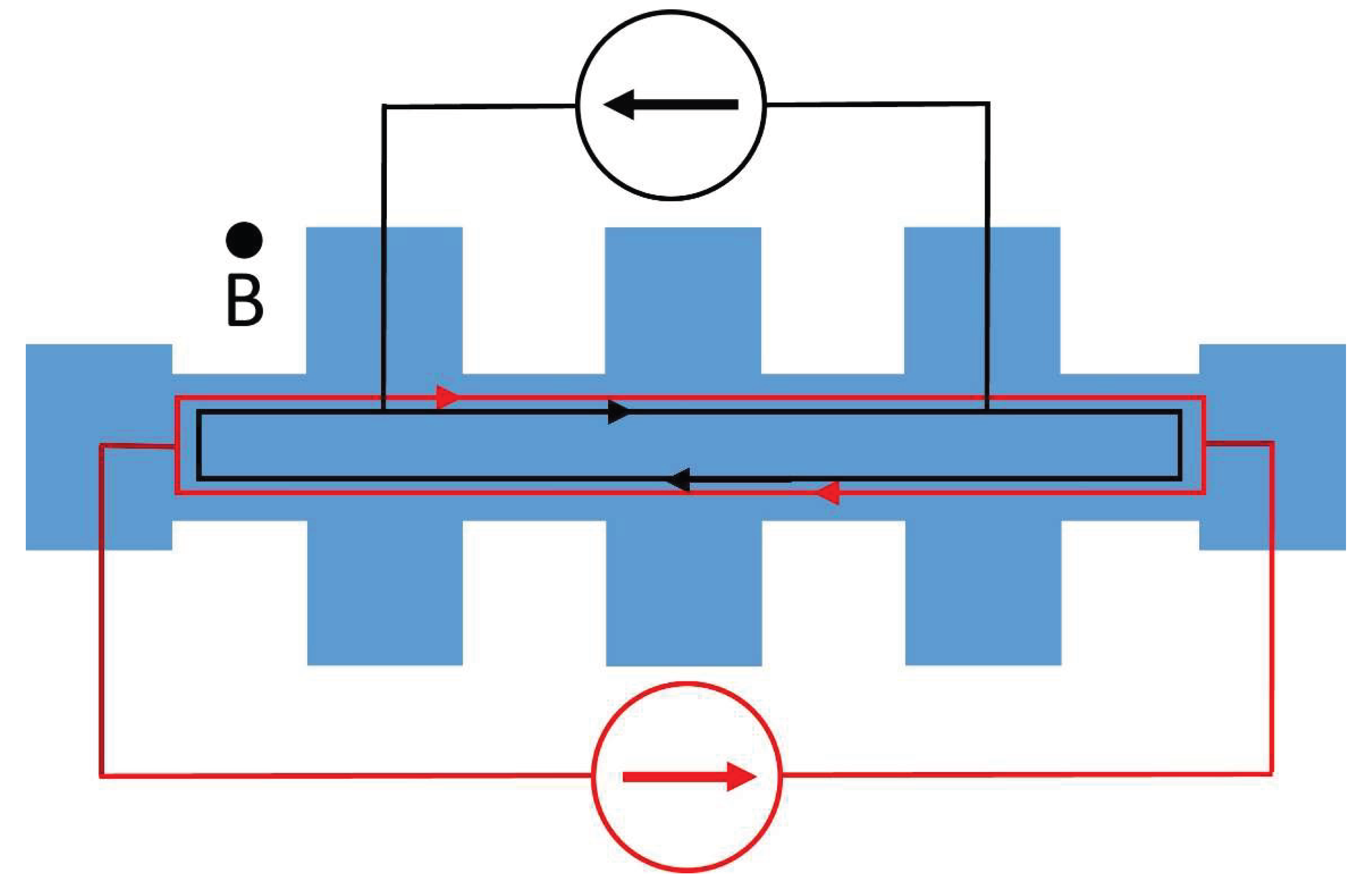
For this study, we used monolayer epitaxial graphene (epigraphene) grown on silicon carbide substrates as the two-dimensional channel [9,10]. The epigraphene was patterned into a Hall bar geometry (Figure 1(a), width = 30 µm, length = 180 µm) using electron-beam lithography and was doped near the charge neutrality point (~5 × 10¹⁰ electrons/cm2) through a molecular doping method (See Figure 1(f)) [32]. This low carrier density enables high mobility, resulting in a robust QHE. After doping, the sample exhibited a carrier mobility of 32,000 cm2/V·s and a sheet resistance of 4 kΩ/□ at a temperature of 2 K. A perpendicular magnetic field was applied to the sample surface to induce a QH state with a filling factor of ν = 2, corresponding to the first plateau in the half-integer QHE of epigraphene [3]. All measurements were performed at T = 2 K using two Keithley current sources and nanovoltmeters.
Before performing the main measurements, we evaluated the contact resistances of all eight terminals on the sample using the three-terminal method under quantum Hall conditions [33]. In the three-terminal method, contact resistance is estimated by measuring the longitudinal resistance with one of the voltage probes placed on the drain contact. Then the measured resistance is the sum of the contact resistance of the drain contact and the lead resistance. All contact resistances were found to be below 10 Ω, except for contact 2 (Rc = 60 Ω), contact 7 (Rc = 60 Ω), and contact 8 (Rc = 40 kΩ) (see Figure 1 for contact numbering). The carrier density extracted from the Hall voltage measured between terminals 2 and 8 was 3.5 × 10¹⁰ electrons/cm2, which deviates from the values obtained using other voltage probes (e.g., terminals 3–7 and 4–6), where the carrier density was approximately 5 × 10¹⁰ electrons/cm2. This discrepancy could be related to the high contact resistance of terminal 8. For the carrier density measurements, current was sourced through contacts 1 and 5. The robustness of the QHE in our sample is further confirmed by the observation of a critical current as high as 5 µA at a magnetic field of 2 T and a temperature of 2 K.
3. Results
Figure 1(a) shows a schematic of the TCS configuration, where the current source A and B supply currents and , which are directed horizontally and vertically, respectively. The voltage measured between terminals 8 and 6 when both current sources are active ( , ) is denoted by . Due to the chirality of the edge currents in the QH regime, we expect that the principle of superposition to hold in the TCS configuration: the voltage when both current sources are on should equal the sum of the voltages measured when each source is applied individually. To test this, we compare with and , where each is measured with the other current source turned off. As shown in Figure 1(b) we find that , consistent with the quantized Hall resistance or zero in the QH state. We further verify this superposition behavior by fixing = 100 nA and varying as 100 nA, 200 nA, 300 nA. The resulting voltage changes accordingly, with remaining constant and varying linearly, as expected (Figure 1(c,d)). The superposition principle is also confirmed at another voltage terminal pair: , where in the QH regime with as shown in Figure 1(e).
We explain the linear superposition behavior observed in the QHE with TCS as shown in Figure 1 using the LBF. In the QH regime at filling factor , the LBF accounts for chiral edge channels that contribute a quantum conductance of , while the bulk remains incompressible. This quantization arises from the half integer QH effect in monolayer graphene, where the Hall conductivity is given by with degeneracy reflecting the spin and valley degeneracy, and the zeroth Landau level () [3]. Within the LBF framework, the current and voltage at each terminal can be expressed as:
(Eq. 1)
Here, denotes the current flowing out of th terminal into the sample, is the voltage at the th terminal, and is the transmission probability for an electron injected from terminal to reach terminal . Charge conservation requires . For dissipationless chiral transport in the QH regime, the transmission probabilities are defined as if and otherwise [30,31]. When both current sources on, LBF allows linear superposition:
, , (Eq. 2)
where and are the total current and voltage at terminal with both sources are on, and , (respectively , ) are those when only source (respectively ) is on. In the specific configuration shown in Figure 1, where and , the LBF gives:
, ,
with zero currents at all other terminals. For the voltages, we find:
for , for
and zero for other terminals. From this, we obtain:
, . Each voltage drop is determined solely by the corresponding current source. These results are in excellent agreement with the experimental observations in Figure 1(b-e).
We investigate additional configurations and conclude that QHE with TCS consistently follows the additive nature of the LBF, regardless of the configuration. In Figure 2, the positions of the current sources are fixed as in Figure 1, but the voltage is measured between terminal 2 and 6. In this set up, both and contain contributions from both longitudinal and transverse conductance arising from current and , respectively. According to the LBF, the superposition of contributions from both sources predicts:
,
indicating that both currents contribute to the Hall voltage. This prediction is verified in Figure 2. In Figure 2(b), the Hall voltage is completely canceled when , consistent with the expected result. Figure 2(c) and 2(d) demonstrate that the Hall voltages can be tuned and made asymmetric by varying the relative magnitudes of the two current sources.
In Figure 3, we explore configurations where the two current sources and are applied parallel (Figure 3(a)) and antiparallel (Figure 3(d)) directions, such that the current either add or cancel. According to the LBF, for the parallel configuration in Figure 3(a), the currents are distributed as:
, ,
with zero currents at all other terminals. The corresponding voltages are:
for , and for
; the other terminals have zero voltage. In this configuration, the expected voltage differences are:
, .
The experimental results in Figure 3(b) and (c) confirm these predictions.
In the antiparallel configuration shown in Figure 3d, only the direction of current for source B is reversed.
and for
; voltages at the other terminals remain zero. The resulting voltage differences are:
and
, which are in excellent agreement with the experimental data shown in Figure 3(e) and (f). These results clearly demonstrate that even when is applied from terminal 4 to terminal 2 in the antiparallel configuration, the current does not flow directly from the short path 4→3→2. Instead, due to the chirality of the edge states, it follows a longer clockwise path: 4→5→6→7→8→1→2.
We further examine a configuration in which the two current sources share a common drain contact, as shown in Figure 4. According to the LBF, the current distribution in this setup is , , with zero currents at all other terminals. The corresponding voltages are for terminals and for . All other terminals have zero voltages. From this, we find the following voltage differences:
,
.
4. Discussion
We explored additional current source configurations and confirmed that the LBF consistently describes transport behavior in all cases. The chiral edge currents along the sample boundary are schematically illustrated in Figure 5 for a configuration where and are nominally applied in opposite directions. Unlike in conventional conductors, where opposing currents may cancel each other, the zero quantum Hall voltages observed in Figure 3(e) and 3(f) do not result from vanishing net current. Instead, they arise from the specific voltage distribution dictated by chiral edge transport, as described by Eq. (1).
5. Conclusions
We have experimentally demonstrated the linear superposition principle of QH transport under TCS excitations in a conventional Hall bar geometry. Our device is based on epitaxial monolayer graphene, doped near the charge neutrality point to enhance mobility and stabilize the QH state. The observed superposition reveals a combinatorial transport behavior in which both longitudinal and transverse QH resistances coexist in a tunable way. This TCS-based approach provides a powerful and flexible method for probing chirality and edge transport in QH systems.
Funding
This work was jointly supported by the IITP under Grant No. RS-2024-00437191, funded by the Ministry of Science and ICT (MSIT), Korea, the faculty research fund of Sejong University in 2025, and the Korean-Swedish Basic Research Cooperative Program of the NRF (No. NRF-2017R1A2A1A18070721), and the Swedish Foundation for Strategic Research (SSF) (No. IS14-0053, GMT14-0077, and RMA15-0024).
Data Availability Statement
We encourage all authors of articles published in MDPI journals to share their research data. In this section, please provide details regarding where data supporting reported results can be found, including links to publicly archived datasets analyzed or generated during the study. Where no new data were created, or where data is unavailable due to privacy or ethical restrictions, a statement is still required. Suggested Data Availability Statements are available in section “MDPI Research Data Policies” at https://www.mdpi.com/ethics.
Acknowledgments
K.H.K. thanks Hans He for fabricating the sample.
Conflicts of Interest
The authors declare no conflicts of interest.
Abbreviations
The following abbreviations are used in this manuscript:
| QHE | Quantum Hall Effect |
| TCS | Two Current Sources |
| LBF | Landauer-Büttiker formalism |
| QH | Quantum Hall |
References
- Tong, D. Lectures on the Quantum Hall Effect; arXiv: 1606.06687, 2016. [Google Scholar]
- von Klitzing, K.; Dorda, G.; Pepper, M. New method for high-accuracy determination of the fine-structure constant based on quantized Hall resistance. Phys. Rev. Lett. 1980, 45, 494–497. [Google Scholar] [CrossRef]
- Zhang, Y.; Tan, Y.-W.; Stormer, H.L.; Kim, P. Experimental observation of the quantum Hall effect and Berry’s phase in graphene. Nature 2005, 438, 201–204. [Google Scholar] [CrossRef]
- Stormer, H.L.; Tsui, D.C.; Gossard, A.C. The fractional quantum Hall effect. Rev. Mod. Phys. 1999, 71, S298–S305. [Google Scholar] [CrossRef]
- von Klitzing, K. The quantum Hall effect—An edge phenomenon? Physica B 1993, 184, 1–6. [Google Scholar] [CrossRef]
- Avron, J.E.; Osadchy, D.; Seiler, R. A topological look at the quantum Hall effect. Phys. Today 2003, 56, 38–43. [Google Scholar] [CrossRef]
- Thouless, D.J.; Kohmoto, M.; Nightingale, M.P.; den Nijs, M. Quantized Hall conductance in a two-dimensional periodic potential. Phys. Rev. Lett. 1982, 49, 405–408. [Google Scholar] [CrossRef]
- Hatsugai, Y. Chern number and edge states in the integer quantum Hall effect. Phys. Rev. Lett. 1993, 71, 3697–3700. [Google Scholar] [CrossRef]
- Tzalenchuk, A.; Lara-Avila, S.; Kalaboukhov, A.; Paolillo, S.; Syväjärvi, M.; Yakimova, R.; Kazakova, O.; Janssen, T.J.B.M.; Fal’ko, V.; Kubatkin, S. Towards a quantum resistance standard based on epitaxial graphene. Nat. Nanotechnol. 2010, 5, 186–189. [Google Scholar] [CrossRef]
- He, H.; Cedergren, K.; Shetty, N.; Lara-Avila, S.; Kubatkin, S.; Bergsten, T.; Eklund, G. Accurate graphene quantum Hall arrays for the new International System of Units. Nat. Commun. 2022, 13, 6933. [Google Scholar] [CrossRef] [PubMed]
- Chang, C.-Z.; et al. Colloquium: Quantum anomalous Hall effect. Rev. Mod. Phys. 2023, 95, 011002. [Google Scholar] [CrossRef]
- Bernevig, B.A.; Zhang, S.-C. Quantum Spin Hall Effect. Phys. Rev. Lett. 2006, 96, 106802. [Google Scholar] [CrossRef]
- Haug, R.J. Edge-state transport and its experimental consequences in high magnetic fields. Semicond. Sci. Technol. 1993, 8, 131–153. [Google Scholar] [CrossRef]
- Ji, Z.; Park, H.; Barber, M.E.; Hu, C.; Watanabe, K.; Taniguchi, T.; Chu, J.-H.; Xu, X.; Shen, Z.-X. Local probe of bulk and edge states in a fractional Chern insulator. Nature 2024, 635, 578–583. [Google Scholar] [CrossRef] [PubMed]
- Ilani, S.; Martin, J.; Teitelbaum, E.; Smet, J.H.; Mahalu, D.; Umansky, V.; Yacoby, A. The microscopic nature of localization in the quantum Hall effect. Nature 2004, 427, 328–332. [Google Scholar] [CrossRef] [PubMed]
- de Picciotto, R.; Reznikov, M.; Heiblum, M.; Umansky, V.; Bunin, G.; Mahalu, D. Direct observation of a fractional charge. Nature 1997, 389, 162–164. [Google Scholar] [CrossRef]
- Garg, M.; Maillet, O.; Samuelson, N.L.; Wang, T.; Feng, J.; Cohen, L.A.; Watanabe, K.; Taniguchi, T.; Roulleau, P.; Sassetti, M.; Zaletel, M.; Young, A.F.; Ferraro, D.; Roche, P.; Parmentier, F.D. Enhanced shot noise in graphene quantum point contacts with electrostatic reconstruction. arXiv 2025, arXiv:2503.17209. [Google Scholar]
- Tang, F.; Ren, Y.; Wang, P.; Zhong, R.; Schneeloch, J.; Yang, S.A.; Yang, K.; Lee, P.A.; Gu, G.; Qiao, Z.; Zhang, L. Three-dimensional quantum Hall effect and metal–insulator transition in ZrTe5. Nature 2019, 569, 537–541. [Google Scholar] [CrossRef]
- Delahaye, F. Series and parallel connection of multiterminal quantum Hall-effect devices. J. Appl. Phys. 1993, 73, 7914–7920. [Google Scholar] [CrossRef]
- Mani, R.G.; von Klitzing, K. Hall effect under null current conditions. Appl. Phys. Lett. 1994, 64, 1262–1264. [Google Scholar] [CrossRef]
- Mani, R.G. Transport study of GaAs/AlGaAs heterostructure- and n-type GaAs-devices in the anti Hall bar within a Hall bar configuration. J. Phys. Soc. Jpn. 1996, 65, 1751–1759. [Google Scholar] [CrossRef]
- Mani, R.G. Experimental technique for realizing dual and multiple Hall effects in a single specimen. Europhys. Lett. 1996, 34, 139–144. [Google Scholar] [CrossRef]
- Mani, R.G. Steady-state bulk current at high magnetic fields in Corbino-type GaAs/AlGaAs heterostructure devices. Europhys. Lett. 1996, 36, 203–208. [Google Scholar] [CrossRef]
- Oswald, M.; Oswald, J.; Mani, R.G. Voltage and current distribution in a doubly connected two-dimensional quantum Hall system. Phys. Rev. B 2005, 72, 035334. [Google Scholar] [CrossRef]
- Oswald, J.; Oswald, M. Magnetotransport in a doubly connected two-dimensional quantum Hall system in the low magnetic field regime. Phys. Rev. B 2006, 74, 153315. [Google Scholar] [CrossRef]
- Uiberacker, C.; Stecher, C.; Oswald, J. Microscopic details of the integer quantum Hall effect in an anti-Hall bar. Phys. Rev. B 2012, 86, 045304. [Google Scholar] [CrossRef]
- Kendirlik, E.M.; Sirt, S.; Kalkan, S.B.; Ofek, N.; Umansky, V.; Siddiki, A. The local nature of incompressibility of quantum Hall effect. Nat. Commun. 2017, 8, 14082. [Google Scholar] [CrossRef]
- Komiyama, S.; Sakuma, H.; Ikushima, K.; Hirakawa, K. Electron temperature of hot spots in quantum Hall conductors. Phys. Rev. B 2006, 73, 045333. [Google Scholar] [CrossRef]
- Rickhaus, P.; Makk, P.; Liu, M.-H.; Tóvári, E.; Weiss, M.; Maurand, R.; Richter, K.; Schönenberger, C. Snake trajectories in ultraclean graphene p–n junctions. Nat. Commun. 2015, 6, 6470. [Google Scholar] [CrossRef]
- Büttiker, M. Absence of backscattering in the quantum Hall effect in multiprobe conductors. Phys. Rev. B 1988, 38, 9375–9389. [Google Scholar] [CrossRef] [PubMed]
- Datta, S. Electronic Transport in Mesoscopic Systems; Cambridge University Press: Cambridge, UK, 1997. [Google Scholar]
- He, H.; Kim, K.H.; Danilov, A.; Montemurro, D.; Yu, L.; Park, Y.W.; Lombardi, F.; Bauch, T.; Moth-Poulsen, K.; Iakimov, T.; Yakimova, R.; Malmberg, P.; Müller, C.; Kubatkin, S.; Lara-Avila, S. Uniform doping of graphene close to the Dirac point by polymer-assisted assembly of molecular dopants. Nat. Commun. 2018, 9, 3956. [Google Scholar] [CrossRef]
- Yager, T.; Lartsev, A.; Cedergren, K.; Yakimova, R.; Panchal, V.; Kazakova, O.; Tzalenchuk, A.; Kim, K.-H.; Park, Y.-W.; Lara-Avila, S.; Kubatkin, S. Low contact resistance in epitaxial graphene devices for quantum metrology. AIP Adv. 2015, 5, 087134. [Google Scholar] [CrossRef]
Figure 1.
(a) Measurement configuration with two current sources in a Hall bar geometry. (b-d) Voltage between terminals 8 and 6 measured for different current combinations: (b) nA, nA; (c), nA , nA (d), nA, nA. (e) Voltage between terminals 2 and 8 for nA, nA. nA denotes the reference current unit. (f) Schematic of the molecular doping, showing multiple layers of poly(methyl methacrylate) (PMMA) and a PMMA+ 2,3,5,6-Tetrafluoro-tetracyano-quino-dimethane (F4TCNQ) blend on top of the epitaxial graphene.
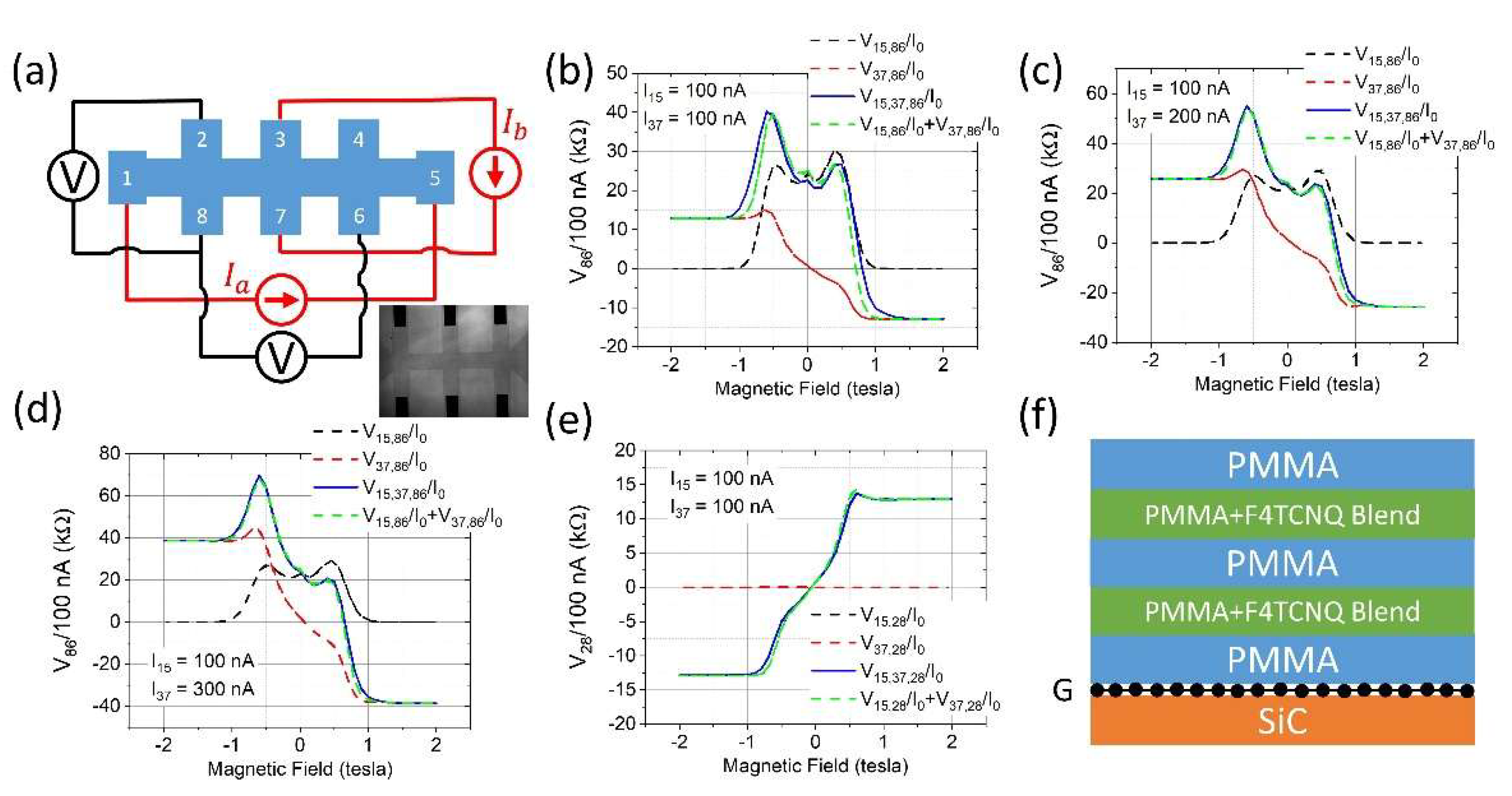
Figure 2.
(a) Measurement configuration with two current sources. (b-d) Voltage between terminals 2 and 6 measured under different conditions: (b) nA, nA (c) nA, nA (d) nA, nA. The reference current nA.
Figure 2.
(a) Measurement configuration with two current sources. (b-d) Voltage between terminals 2 and 6 measured under different conditions: (b) nA, nA (c) nA, nA (d) nA, nA. The reference current nA.
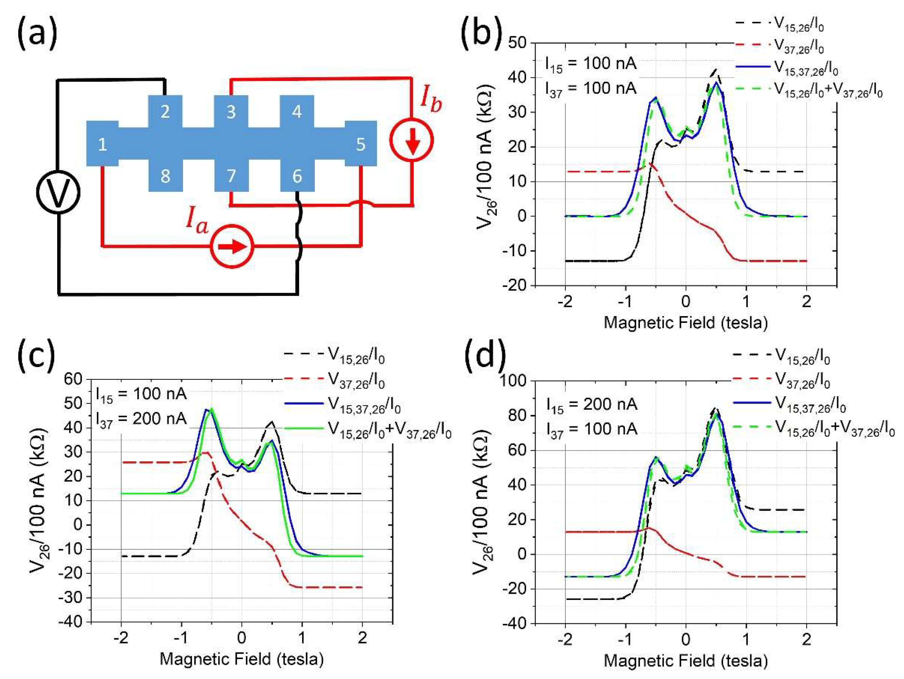
Figure 3.
(a) Measurement configuration for the parallel injection case, corresponding to panels (b) and (c). (b) Voltage between terminals 8 and 6 measured with nA and nA. (c) Voltage between terminals 3 and 7 under the same parallel current conditions. (d) Measurement configuration for the antiparallel current injection case, corresponding to panels (e) and (f). (e) Voltage between terminals 8 and 6 with nA and nA. (f) Voltage between terminals 3 and 7 under the same antiparallel conditions. The reference current nA.
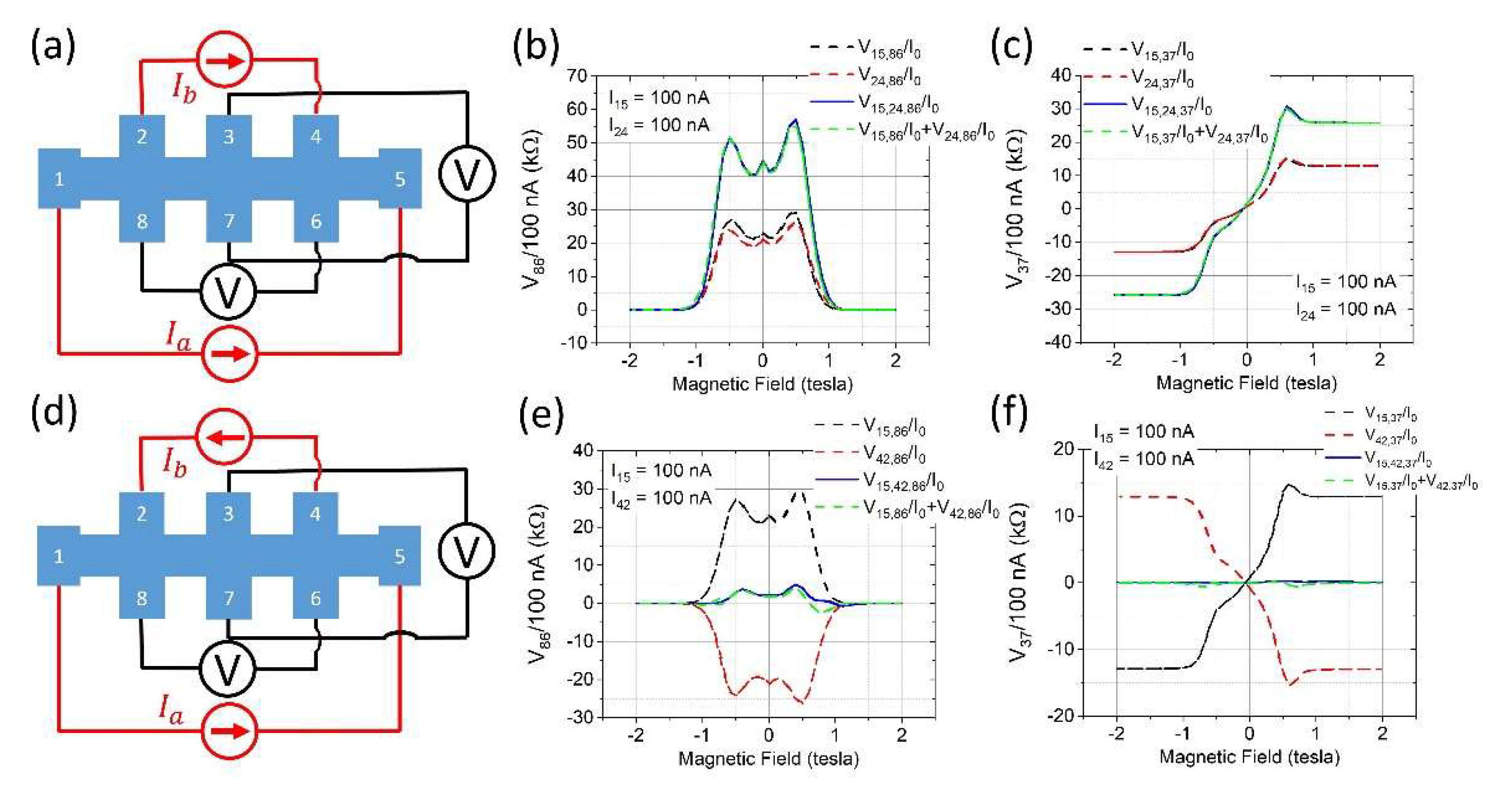
Figure 4.
Measurement configuration where two current sources share a common drain. (a) Setup corresponding to the measurement shown in (b). (b) Voltage between terminals 2 and 3 with 100 nA and 100 nA. (c) Setup corresponding to the measurement shown in (d). (d) Voltage between terminals 2 and 7 with 100 nA and 100 nA. The reference current 100 nA.
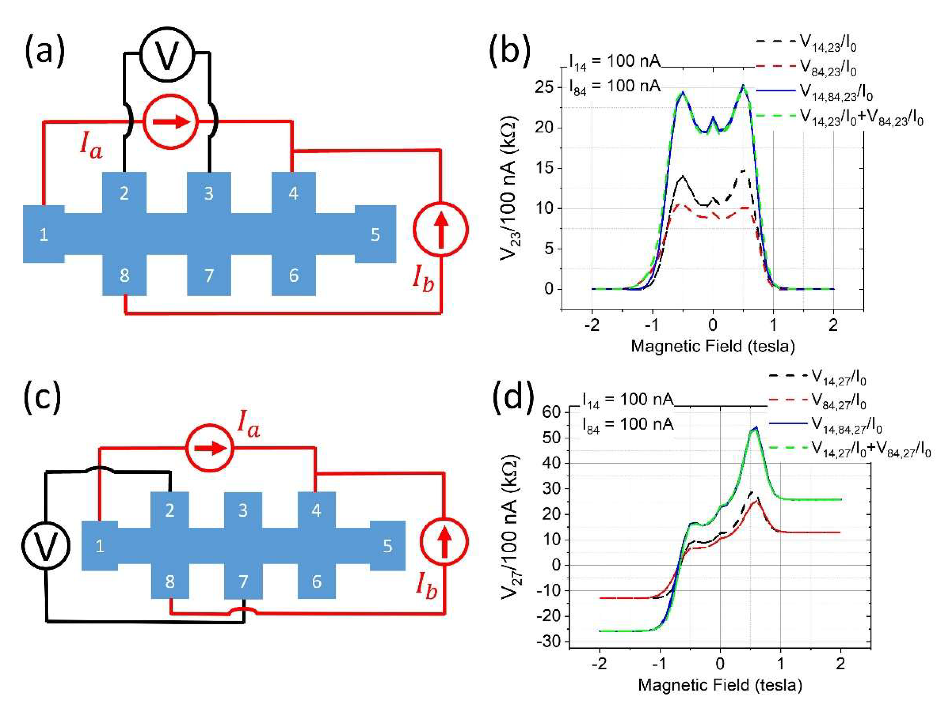
Figure 5.
Schematic of current distribution in multiple current source excitation configuration. Each current from the respective source follows the same chiral edge direction, resulting in the additive behavior of the QHE.
Figure 5.
Schematic of current distribution in multiple current source excitation configuration. Each current from the respective source follows the same chiral edge direction, resulting in the additive behavior of the QHE.
Disclaimer/Publisher’s Note: The statements, opinions and data contained in all publications are solely those of the individual author(s) and contributor(s) and not of MDPI and/or the editor(s). MDPI and/or the editor(s) disclaim responsibility for any injury to people or property resulting from any ideas, methods, instructions or products referred to in the content. |
© 2025 by the authors. Licensee MDPI, Basel, Switzerland. This article is an open access article distributed under the terms and conditions of the Creative Commons Attribution (CC BY) license (http://creativecommons.org/licenses/by/4.0/).
Copyright: This open access article is published under a Creative Commons CC BY 4.0 license, which permit the free download, distribution, and reuse, provided that the author and preprint are cited in any reuse.


