
Submitted:
28 July 2025
Posted:
28 July 2025
You are already at the latest version
Abstract
Studies on two-dimensional materials (such as topological insulators or transition metal dichalcogenides) have shown that they exhibit unique properties, including high charge carrier mobility and tunable bandgaps, making them attractive for next-generation electronics. Some of these materials (e.g., HfSe2) also offer thickness-dependent bandgap engineering. However, the standard device fabrication techniques often introduce processing contamination, which reduces device efficiency. In this paper, we present a modified mechanical exfoliation technique, the Reversed Structuring Procedure, which enables the fabrication of hybrid systems based on 2D micro-flakes with improved interface cleanliness and contact quality. Hall effect measurements on Bi2Se3 and HfSe2 devices confirm enhanced electrical performance, including increased carrier mobility. We also introduce a novel Star-Shaped Electrode Structure, which allows for accurate Hall measurements and the exploration of geometric magnetoresistance effects within the same device. This dual-purpose geometry enhances the flexibility and demonstrates broader functionality of the proposed fabrication method. The presented results validate the Reversed Structuring Procedure method as a robust and versatile approach for 2D material-based electronic and sensing applications.
Keywords:
layered materials
; mechanical exfoliation
; Hall effect
; topological insulators
; transition metal dichalcogenides
; geometrical magnetoresistance
1. Introduction
Two-dimensional (2D) materials have emerged as one of the most promising groups of materials for electronic applications, due to their tunable electronic properties and the ease of bandgap engineering [1]. The development of this class of materials began with the discovery of graphene by Novoselov et al. [2], which marked a significant milestone in semiconductor technology, enabling improved physical and electrical properties in nanoelectronics [3,4,5,6]. Beyond graphene, the family of 2D materials includes other advanced materials such as topological insulators (TIs) and transition metal dichalcogenides (TMDs) [7,8,9,10,11,12]. These materials are considered highly promising for next-generation hybrid electronic devices, including sensor platforms, where 2D material layers (or flakes) serve as the active channel [13,14]. A key parameter in the considered applications is charge carrier mobility at room temperature (RT) which has been predicted as for graphene [2], for bismuth selenide (Bi2Se3) [15], and ) for hafnium diselenide (HfSe2) [16]. Unlike graphene, which is semi-metallic regardless of thickness, the electronic properties of TIs and TMDs are highly dependent on the number of layers, with transitions from semiconducting to semi-metallic properties observed as the thickness increases [17,18,19].
The weak physical interactions between layers in 2D crystals enable the separation of single or few-layer flakes through mechanical exfoliation from bulk crystals [20]. This technique, initially demonstrated using adhesive tape for graphene [2,21,22], has been successfully adopted for other 2D materials, also for surface preparation [23,24]. The exfoliated flakes (layers) can then be transferred onto an insulating substrate and structured to form the active channels in microelectronic devices. In previous work, our research group has employed such a structuring approaches to fabricate 2D-materials-based sensors [24,25,26]. Mechanical exfoliation remains attractive due to its simplicity and accessibility, requiring no specialised equipment. However, parameters such as tape adhesion, transfer pressure, peeling speed, and ambient exposure time significantly affect the size, quality, and cleanliness of the transferred flakes [22,27]. Residual contamination, such as adhesive residues, can severely degrade contact quality and reduce the achievable electronic performance. As a result, enhancing exfoliation and transfer procedures to minimise surface contamination and structural defects remains a major challenge.
Several modified exfoliation and transfer techniques have been developed to address these issues. These include the use of polymeric supports such as polymethyl methacrylate (PMMA), PMMA-based water-soluble tapes, or even metallic (e.g., gold) transfer layers [27,28,29,30,31]. Despite improvements, complete removal of contaminants and preservation of pristine surface properties remain difficult. Surface impurities and defects not only degrade electrical performance but also reduce the mechanical stability of metal contacts [32,33]. Hence, chemical cleaning steps are often used before further device processing steps [26,29].
This study presents an elaborated Reversed Structuring Procedure (RSP), developed to improve the fabrication of microdevices based on 2D-material flakes. This method simplifies the process, reduces atmospheric exposure of the flake’s surface, and limits the impact of transfer-related contamination. The effects of the RSP method have been compared with the Standard Structuring Procedure (SSP) by fabricating and analysing several Hall structures based on Bi2Se3 (TI) and HfSe2 (TMD) flakes. Charge carrier mobility and concentration were estimated using Hall-effect measurements to evaluate the effectiveness of both procedures. The results demonstrate that the RSP significantly improves device performance, particularly for materials with chemically sensitive surfaces such as HfSe2. In addition, the star-shaped electrode structure (SSES) was introduced and used for device fabrication and characterisation. The SSES enables symmetrical current distribution and offers versatility in measurement configurations. While similar star-shaped geometries have been used for thin-film measurements [34,35], our approach applies this geometry in combination with the RSP. The SSES provides a flexible platform for evaluating transport properties, enabling reliable measurements for both Hall and geometric magnetoresistance (gMR) effects. Although the SSES is not proposed as a novel geometry, we highlight its utility as a dual-purpose platform for experimental validation of the structuring procedures.
2. Materials and Methods
The paper is focused on the experimental comparison of the SSP and the newly proposed RSP method. Both methods are based on fabricating a hybrid structure on a mechanically exfoliated micro-flake of the 2D material (Bi2Se3 and HfSe2). Figure 1 shows the SSP procedure in detail. The SSP consists of two stages: fabrication of the active channel (Figure 1a) and the formation of metallic contacts (electrodes) (Figure 1b). The thin flake was exfoliated from the 3D bulk crystal using adhesive tape during the first step. The exfoliation continued layer by layer until the flake reached sufficient thinness while maintaining mechanical integrity. The flake fabricated in this way was cut from the adhesive tape with a scalpel and transferred onto an insulating (or semi-insulating) substrate (e.g., ). To avoid contamination during the transfer process, the transfer tape was carefully separated to limit its negative impact on subsequent steps. Next, the flake—still supported by tape—was aligned and pressed onto the substrate using a pressure-controlled device to promote van der Waals bonding (using controlled pressure adjustment to achieve a repeatable procedure). After one hour, the pressure was released, and the tape was removed under an optical microscope using a needle. Finally, residual impurities were removed by sequential 1-minute baths in acetone and isopropanol, followed by compressed air drying to prepare the system for a further structuring process (Figure 1b).
The second process (formation of the electrodes) of the SSP is presented in detail in Figure 1b. For this purpose, the substrate with the deposited flake was coated with a resist layer (AR-P 3510 T, AllResist), diluted 1:1 with Milli-Q water, and spin-coated at 2000 rpm for 1 min. The resist layer was thermally treated to remove diluent (at 100 °C for 1 min). In the next step, the optical lithography was used to pattern the electrodes. The resist layer development procedure was performed using dedicated reagents. The electrodes (buffer layer 40 nm Cr and the outer electrode 400 nm Au for Bi2Se3 and a 20 nm Ni buffer layer combined with outer electrode 120 nm Au for HfSe2) were deposited using the DC magnetron sputtering method under high vacuum conditions. The lift-off process was carried out in an acetone bath. The final effects of the SSP procedure are presented in Figure 2.
The SSP method requires adapting the electrode pattern to match the individual shape and position of each deposited flake. Moreover, there is a risk of mechanical damage to the flake and its detachment from the substrate during structure processing. Furthermore, residual contamination after the flake transfer impairs contact quality between the flake and the deposited electrodes. These limitations significantly reduce fabrication reproducibility and device yield, motivating the development of a more robust approach. To address these issues, we developed a modified procedure—referred to as the RSP method—outlined in Figure 3. Unlike the SSP method, the first step of the RSP process focuses on the fabrication of the electrodes on top of an insulating substrate (Figure 3a).
To match the reduced thickness of electrodes in the RSP method, the photoresist parameters were adjusted to achieve a 400 nm layer—thinner than in the SSP approach (using a 1:5 dilution of photoresist in Milli-Q water, spin-coated at 4000 rpm for 1 minute). The fabricated electrodes consisted of 20 nm Ni buffer layer, covered by a 60 nm Au top electrode (Figure 3a). The second process of the RSP was the deposition of a flake in the centre of the electrode system. The flake exfoliation procedure was similar to that in the SSP method, with one modification (Figure 3b). The standard adhesive tape could damage the electrode system due to the reversed deposition geometry. To allow for easy removal, a water-soluble transfer tape (3M 5414 TRANSPARENT 1/2IN) was used. As mentioned above, the flake position on the electrode structure is crucial for device functionality. Therefore, optical microscopy was used for precise alignment to provide electrical contact quality before the mechanical pressing was applied. The flake was cleaned in an ultrasonic bath: 1 hour in Milli-Q water at 80 °C followed by 1-minute baths in acetone and isopropanol to remove transfer tape and other contaminants from the process. Finally, compressed air drying was applied, and the final results are shown in Figure 4b-c.
The RSP method offers several distinct advantages over the SSP approach. By reversing the fabrication sequence, the RSP enables the use of a universal SSES electrode pattern for various flake positions. This pattern consists of 12 pairs of electrodes (see Figure 4a). The RSP allows tuning of the electrode composition to enhance flake–electrode interaction and improve mechanical stability. Moreover, the exposure time of the exfoliated surface to ambient pressure is shortened, and the interface flake-electrode is not contaminated by transfer residuals in this procedure. Overall, the RSP approach was developed to address the inherent limitations of SSP, including poor contact reliability, contamination at the flake–electrode interface, and mechanical instability during processing. In the following sections, we compare the electrical performance of both methods with emphasis on Hall mobility and magnetoresistance to evaluate the practical effectiveness of the RSP technique.
Commercially available high-quality single crystals of Bi2Se3 and HfSe2 were used as source materials for the exfoliation of 2D flakes. The monocrystals were grown using the Chemical Vapour Deposition (CVD) method and supplied by HQ Graphene (Netherlands). Bi2Se3 (TI) and HfSe2 (TMD) were selected to represent two distinct classes of layered materials with differing charge transport mechanisms. In addition, the HfSe2 surface is extremely susceptible to oxidation under ambient conditions.
Hall effect measurements of all fabricated structures were performed at RT and in a fixed magnetic field ( T) using the Hall effect analyser Linseis HCS-1. Based on these measurements, the sheet carrier density was determined as follows:
where B is the magnetic field (T), I is the current (A), q is the elementary charge (C), and is the Hall voltage (V). The charge carrier mobility was determined using:
where is the sheet resistance (), determined using the van der Pauw (vdP) method [36].
The gMR is defined as the change of the electrical resistance in a certain magnetic field compared to the electrical resistance in the absence of a magnetic field. The resistance of a device for any terminal arrangement is defined as , with the indices i, j denoting driving current terminal numbers and the indices k, l denoting voltage terminal numbers. The gMR is defined as:
where is the electric resistance of a device in the absence of a magnetic field.
3. Results and Discussion
Four hybrid structures were fabricated to compare the Hall performance of the SSP and RSP methods, utilising active channels on different layered materials classes Bi2Se3 and HfSe2. Due to the small size of the exfoliated Bi2Se3 flakes, SSP-fabricated structures used a standard four-electrode Hall-cross configuration (Figure 2a). In other cases, the 12-electrode SSES layout was used, enabling precise positioning of the micro-flake between opposing electrode pairs for Hall measurements (Figure 2b and Figure 4). Representative devices based on Bi2Se3 and HfSe2 are shown in both Figure 2 and Figure 4.
Table 1 presents the results of Hall effect measurements, including sheet carrier density and mobility, for all considered samples. For the 4-electrode Bi2Se3 structure, Hall measurements were performed using the conventional method: opposing terminals were used to measure the Hall voltage while sequential terminal pairs were used in the van der Pauw (vdP) configuration to determine the sheet resistance. In the case of devices with the 12-electrode SSES layout, two pairs of opposing electrodes were selected to perform Hall and resistance measurements. Although the presence of additional electrodes in the SSES configuration may introduce minor perturbations in the measured Hall voltage these effects are expected to be of the same order across all SSES-based structures.
The data in Table 1reveal a consistent trend in carrier mobility across all samples. For both types of tested layered materials, the carrier mobility values were consistently higher for structures fabricated using the RSP method compared to SSP. However, they deviate significantly from the theoretical values reported in literature for pristine systems, especially in the case of the HfSe2-based device. The possible explanation of this effect could be the rapid surface oxidation, as it has already been proven to be a highly reactive substrate [16,37]. Forming an electrical contact with a 2D material is more challenging than with conventional 3D semiconductors. Ang et al. demonstrated that the effect of interfacial charge carriers injection through the contact barrier could improve the electrical characteristic of the contact by lowering the height of the Schottky barrier on the interface between 2D material and metal [38]. Charge carrier injection from a 3D metallic electrode into a 2D semiconductor can impact whether the semiconductor is 2D metallised through direct contact with metal. In the case of a van der Waals interface, at the contact interface, a Schottky barrier forms and reduces the efficiency of the charge carrier injection process [38]. In addition, the edge contact is more efficient in the case of 2D materials, particularly for chemically inert or oxidized surfaces [38]. By fabricating hybrid structures using the RSP method, the formation of edge contacts is facilitated by pressing the micro-flake into the electrode, thereby reducing the probability of damage. This effect improves the contact quality, decreases the Schottky barrier, and improves the efficiency of charge carriers’ injection into the layered material. The consequence is an improvement in the mobility of charge carriers, which is observed by comparing the results of Hall effect measurements for the structures fabricated using the SSP and RSP approaches for both considered layered materials.
The potential of the SSES structure for investigating the gMR effect is assessed based on the data presented in Figure 5.
The metal–semiconductor hybrid structure can be considered a magnetoresistive system where the geometric contribution dominates over intrinsic (physical) magnetoresistive effects. Several similarities can be identified between the SSES layout and extraordinary magnetoresistance (EMR) geometries, including the so-called raster geometry [24]. In all these systems, the structures have a set of connection terminals and a specific arrangement of a metallic non-magnetic shunt. In the case of SSES, the role of the metallic shunt is played by auxiliary electrodes.
Figure 5 presents the application of the SSES structure for investigating the gMR effects in a Bi2Se3 micro-flake-metal hybrid system. There is an observed characteristic increase in gMR for the asymmetric configuration when the voltage electrodes are approached symmetrically to one of the current electrodes. By analogy with the planar EMR configuration [39,40], to illustrate and confirm the gMR effect, three asymmetric connection configurations were selected: BD15, BD27, BDAC (terminals notation consistent with the terminal description in Figure 4a). The BD15 configuration represents the longest distance between the voltage terminals relative to terminal D, ACBD the average distance, and 27BD the shortest distance.
4. Conclusions
This paper presents an alternative approach to the fabrication of electrical devices based on 2D materials. The proposed RSP modifies the standard process sequence by forming the electrode system before transferring the active 2D micro-flake. Hall effect measurements confirmed enhanced electrical performance of RSP-fabricated devices, including notably higher charge carrier mobility. The observed improvements are attributed to the cleaner electrode-flake interface achieved by minimising exposure to atmospheric conditions and enabling the formation of more effective edge contacts, thus reducing the Schottky barrier and facilitating carrier injection. This is particularly beneficial for reactive layered materials such as HfSe2.
Moreover, integration of an SSES into the RSP expands the functionality of the devices. This geometry enables multi-point measurements, enhancing flexibility in studying charge transport properties. In addition to Hall effect characterisation, SSES allows investigation of gMR phenomena. The measured gMR responses, especially in asymmetric connection configurations, demonstrate the potential of this design for use in hybrid magnetic sensing systems. Together, these results emphasise that the RSP, in combination with SSES, not only simplifies fabrication but also improves the physical interface and extends measurement capabilities, establishing this approach as a promising platform for future applications in 2D-material-based sensors and nanoelectronic devices.
Author Contributions
Conceptualization,—PK, JR, SA, WK; methodology,—PK, JR; validation,—SA, WK; formal analysis, —SA, WK; investigation,—PK, JR, SA; resources,—WK; data curation,—JR, SA, KK, WR, AŻ; writing—original draft preparation,—PK, JR, SA, WK; writing—review and editing,—PK, JR, SA, WK; visualization,—PK, JR, MP, AŻ; supervision,—WK; project administration,—WK; funding acquisition,—WK. All authors have read and agreed to the published version of the manuscript.
Funding
The research has received funding from the Ministry of Education and Science (Poland) under Projects No. 0512/SBAD/2420.
Data Availability Statement
The raw/processed data required to reproduce the above findings cannot be shared at this time as the data also form part of an ongoing study.
Conflicts of Interest
The authors declare no conflicts of interest.
Abbreviations
The following abbreviations are used in this manuscript:
| 2D | two-dimensional |
| Bi2Se3 | Bismuth selenide |
| HfSe2 | Hafnium diselenides |
| TI | Topological insulators |
| TMD | Transition metal dichalcogenide |
| RT | Room temperature |
| PMMA | Polymethyl methacrylate |
| RSP | Reversed structuring procedure |
| SSP | Standard structuring procedure |
| SSES | Star-shaped electrode structure |
| CVD | Chemical Vapour Deposition |
| gMR | Geometric magnetoresistance |
| EMR | Extraordinary magnetoresistance |
References
- Fiori, G.; Bonaccorso, F.; Iannaccone, G.; Palacios, T.; Neumaier, D.; Seabaugh, A.; Banerjee, S.K.; Colombo, L. Electronics based on two-dimensional materials. Nature Nanotechnology 2014, 9, 768–779. [Google Scholar] [CrossRef]
- Novoselov, K.S.; Geim, A.K.; Morozov, S.V.; Jiang, D.; Zhang, Y.; Dubonos, S.V.; Grigorieva, I.V.; Firsov, A.A. Electric Field Effect in Atomically Thin Carbon Films. Science 2004, 306, 666–669. [Google Scholar] [CrossRef] [PubMed]
- Reddig, W.; Przychodnia, M.; Ciuk, T.; El-Ahmar, S. High-temperature Stability of Sensor Platforms Designed to Detect Magnetic Fields in A Harmful Radiation Environment. IEEE Sensors Letters 2023, 7, 1–4. [Google Scholar] [CrossRef]
- Akinwande, D.; Brennan, C.J.; Bunch, J.S.; Egberts, P.; Felts, J.R.; Gao, H.; Huang, R.; Kim, J.S.; Li, T.; Li, Y.; et al. A review on mechanics and mechanical properties of 2D materials—Graphene and beyond. Extreme Mechanics Letters 2017, 13, 42–77. [Google Scholar] [CrossRef]
- El-Ahmar, S.; Szary, M.J.; Ciuk, T.; Prokopowicz, R.; Dobrowolski, A.; Jagiełło, J.; Ziemba, M. Graphene on SiC as a promising platform for magnetic field detection under neutron irradiation. Applied Surface Science 2022, 590, 152992. [Google Scholar] [CrossRef]
- El-Ahmar, S.; Przychodnia, M.; Jankowski, J.; Prokopowicz, R.; Ziemba, M.; Szary, M.J.; Reddig, W.; Jagiełło, J.; Dobrowolski, A.; Ciuk, T. The Comparison of InSb-Based Thin Films and Graphene on SiC for Magnetic Diagnostics under Extreme Conditions. Sensors 2022, 22, 5258. [Google Scholar] [CrossRef]
- Wang, M.X.; Liu, C.; Xu, J.P.; Yang, F.; Miao, L.; Yao, M.Y.; Gao, C.L.; Shen, C.; Ma, X.; Chen, X.; et al. The coexistence of superconductivity and topological order in the Bi2Se3 thin films. Science 2012, 335, 52–55. [Google Scholar] [CrossRef] [PubMed]
- Qi, X.L.; Zhang, S.C. Topological insulators and superconductors. Reviews of Modern Physics 2011, 83. [Google Scholar] [CrossRef]
- Chhowalla, M.; Liu, Z.; Zhang, H. Two-dimensional transition metal dichalcogenide (TMD) nanosheets. Chemical Society Reviews 2015, 44, 2584–2586. [Google Scholar] [CrossRef]
- Pi, L.; Li, L.; Liu, K.; Zhang, Q.; Li, H.; Zhai, T. Recent Progress on 2D Noble-Transition-Metal Dichalcogenides. Advanced Functional Materials 2019, 29, 1–22. [Google Scholar] [CrossRef]
- Huang, H.H.; Fan, X.; Singh, D.J.; Zheng, W.T. Recent progress of TMD nanomaterials: Phase transitions and applications. Nanoscale 2020, 12, 1247–1268. [Google Scholar] [CrossRef]
- Raczyński, J.; Nowak, E.; Nowicki, M.; El-Ahmar, S.; Szybowicz, M.; Koczorowski, W. Studies of temperature-dependent Raman spectra of thin PtSe2 layers on Al2O3 substrate. Materials Science and Engineering B 2023, 297, 116728. [Google Scholar] [CrossRef]
- Culcer, D. Transport in three-dimensional topological insulators: Theory and experiment. Physica E: Low-Dimensional Systems and Nanostructures 2012, 44, 860–884. [Google Scholar] [CrossRef]
- Ilatikhameneh, H.; Tan, Y.; Novakovic, B.; Klimeck, G.; Rahman, R.; Appenzeller, J. Tunnel Field-Effect Transistors in 2-D Transition Metal Dichalcogenide Materials. IEEE Journal on Exploratory Solid-State Computational Devices and Circuits 2015, 1, 12–18. [Google Scholar] [CrossRef]
- Liu, Y.; Xu, Y.; Ji, Y.; Zhang, H. Monolayer Bi2Se3-xTex: Novel two-dimensional semiconductors with excellent stability and high electron mobility. Physical Chemistry Chemical Physics 2020, 22, 9685–9692. [Google Scholar] [CrossRef]
- Mirabelli, G.; McGeough, C.; Schmidt, M.; McCarthy, E.K.; Monaghan, S.; Povey, I.M.; McCarthy, M.; Gity, F.; Nagle, R.; Hughes, G.; et al. Air sensitivity of MoS2, MoSe2, MoTe2, HfS2, and HfSe2. Journal of Applied Physics 2016, 120. [Google Scholar] [CrossRef]
- Mirõ, P.; Ghorbani-Asl, M.; Heine, T. Two dimensional materials beyond MoS2: Noble-transition-metal dichalcogenides. Angewandte Chemie - International Edition 2014, 53, 3015–3018. [Google Scholar] [CrossRef]
- Villaos, R.A.B.; Crisostomo, C.P.; Huang, Z.Q.; Huang, S.M.; Padama, A.A.B.; Albao, M.A.; Lin, H.; Chuang, F.C. Thickness dependent electronic properties of Pt dichalcogenides. npj 2D Materials and Applications 2019, 3, 1–8. [Google Scholar] [CrossRef]
- Pandey, S.K.; Das, R.; Mahadevan, P. Layer-Dependent Electronic Structure Changes in Transition Metal Dichalcogenides: The Microscopic Origin. ACS Omega 2020, 5, 15169–15176. [Google Scholar] [CrossRef] [PubMed]
- Lv, R.; Robinson, J.A.; Schaak, R.E.; Sun, D.; Sun, Y.; Mallouk, T.E.; Terrones, M. Transition metal dichalcogenides and beyond: Synthesis, properties, and applications of single- and few-layer nanosheets. Accounts of Chemical Research 2015, 48, 56–64. [Google Scholar] [CrossRef]
- Yi, M.; Shen, Z. A review on mechanical exfoliation for the scalable production of graphene. Journal of Materials Chemistry A 2015, 3, 11700–11715. [Google Scholar] [CrossRef]
- Gao, E.; Lin, S.Z.; Qin, Z.; Buehler, M.J.; Feng, X.Q.; Xu, Z. Mechanical exfoliation of two-dimensional materials. Journal of the Mechanics and Physics of Solids 2018, 115, 248–262. [Google Scholar] [CrossRef]
- Kwiecień, K.; Koczorowski, W.; Grzela, T. Effect of surface preparation on PtSe2 crystal surface morphology. Surface Science 2022, 727, 122181. [Google Scholar] [CrossRef]
- El-Ahmar, S.; Koczorowski, W.; Poźniak, A.A.; Kuświk, P.; Strupiński, W.; Czajka, R. Graphene-based magnetoresistance device utilizing strip pattern geometry. Applied Physics Letters 2017, 110, 043503–5. [Google Scholar] [CrossRef]
- Koczorowski, W.; Raczyński, J.; El-Ahmar, S.; Nowicki, M.; Szybowicz, M.; Czajka, R. Processing of PtSe2 ultra-thin layers using Ar plasma. Materials Science in Semiconductor Processing 2023, 167, 107814. [Google Scholar] [CrossRef]
- Koczorowski, W.; Kuświk, P.; Przychodnia, M.; Wiesner, K.; El-Ahmar, S.; Szybowicz, M.; Nowicki, M.; Strupiński, W.; Czajka, R. CMOS- compatible fabrication method of graphene-based micro devices. Materials Science in Semiconductor Processing 2017, 67, 92–97. [Google Scholar] [CrossRef]
- Li, Y.; Kuang, G.; Jiao, Z.; Yao, L.; Duan, R. Recent progress on the mechanical exfoliation of 2D transition metal dichalcogenides. Materials Research Express 2022, 9. [Google Scholar] [CrossRef]
- Schranghamer, T.F.; Sharma, M.; Singh, R.; Das, S. Review and comparison of layer transfer methods for two-dimensional materials for emerging applications, 2021. [CrossRef]
- Zhang, R.; Chen, T.; Bunting, A.; Cheung, R. Optical lithography technique for the fabrication of devices from mechanically exfoliated two-dimensional materials. Microelectronic Engineering 2016, 154, 62–68. [Google Scholar] [CrossRef]
- Desai, S.B.; Madhvapathy, S.R.; Amani, M.; Kiriya, D.; Hettick, M.; Tosun, M.; Zhou, Y.; Dubey, M.; Ager, J.W.; Chrzan, D.; et al. Gold-Mediated Exfoliation of Ultralarge Optoelectronically-Perfect Monolayers. Advanced Materials 2016, 28, 4053–4058. [Google Scholar] [CrossRef]
- Liu, F.; Wu, W.; Bai, Y.; Chae, S.H.; Li, Q.; Wang, J.; Hone, J.; Zhu, X.Y. Disassembling 2D van der Waals crystals into macroscopic monolayers and reassembling into artificial lattices. Science 2020, 367, 903–906. [Google Scholar] [CrossRef] [PubMed]
- Zhao, Y.; Qiao, J.; Yu, Z.; Yu, P.; Xu, K.; Lau, S.P.; Zhou, W.; Liu, Z.; Wang, X.; Ji, W.; et al. High-electron-mobility and air-stable 2D layered PtSe2 FETs. Advanced Materials 2017, 29, 1604230. [Google Scholar] [CrossRef]
- Wang, Z.; Li, Q.; Besenbacher, F.; Dong, M. Facile synthesis of single crystal PtSe2 nanosheets for nanoscale electronics. Advanced Materials 2016, 28, 10224–10229. [Google Scholar] [CrossRef]
- Chen, X.; Xiaofeng, Z.; Cheng, R.; Zhang, J.; Wu, Y.; Ba, Y.; Li, H.; Sun, Y.; You, Y.; Zhao, Y.; et al. Electric field control of Néel spin–orbit torque in an antiferromagnet. Nature Materials 2019, 18, 931–935. [Google Scholar] [CrossRef]
- Nam, G.; He, Q.; Wang, X.; Yu, Y.; Junze, C.; Zhang, K.; Yang, Z.; Hu, D.; Lai, Z.; Li, B.; et al. In-Plane Anisotropic Properties of 1T’-MoS2 Layers. Advanced Materials 2019, 31, 2–7. [Google Scholar] [CrossRef] [PubMed]
- van der Pauw, L.J. A method of measuring specific resistivity and Hall effect of discs of aribtrary shape. Philips Research Reports 1958, 13, 1–11. [Google Scholar]
- Kwiecień, K.; Raczyński, J.; Puchalska, A.; Nowak, E.; Chłopocka, E.; Kot, D.; Szybowicz, M.; Jurczyszyn, L.; Koczorowski, W. The effects of short-term air exposure of the monocrystal HfSe2 surface. Applied Surface Science 2025, 690, 162546. [Google Scholar] [CrossRef]
- Ang, Y.S.; Cao, L.; Ang, L.K. Physics of electron emission and injection in two-dimensional materials: Theory and simulation. InfoMat 2021, 3, 502–535. [Google Scholar] [CrossRef]
- Oszwaldowski, M.; El-Ahmar, S.; Jankowski, J. Extraordinary magnetoresistace in planar configuration. Journal of Physics D: Applied Physics 2012, 45, 145002. [Google Scholar] [CrossRef]
- El-Ahmar, S.; Koczorowski, W.; Poźniak, A.; Kuświk, P.; Przychodnia, M.; Dembowiak, J.; Strupiński, W. Planar configuration of extraordinary magnetoresistance for 2D-material-based magnetic field sensors. Sensors and Actuators A: Physical 2019, 296, 249–253. [Google Scholar] [CrossRef]
Figure 1.
Schematic presentation of the standard structuring procedure (SSP) using an exfoliated flake as an on-bottom active channel in the device. Detailed description in the manuscript text.
Figure 1.
Schematic presentation of the standard structuring procedure (SSP) using an exfoliated flake as an on-bottom active channel in the device. Detailed description in the manuscript text.
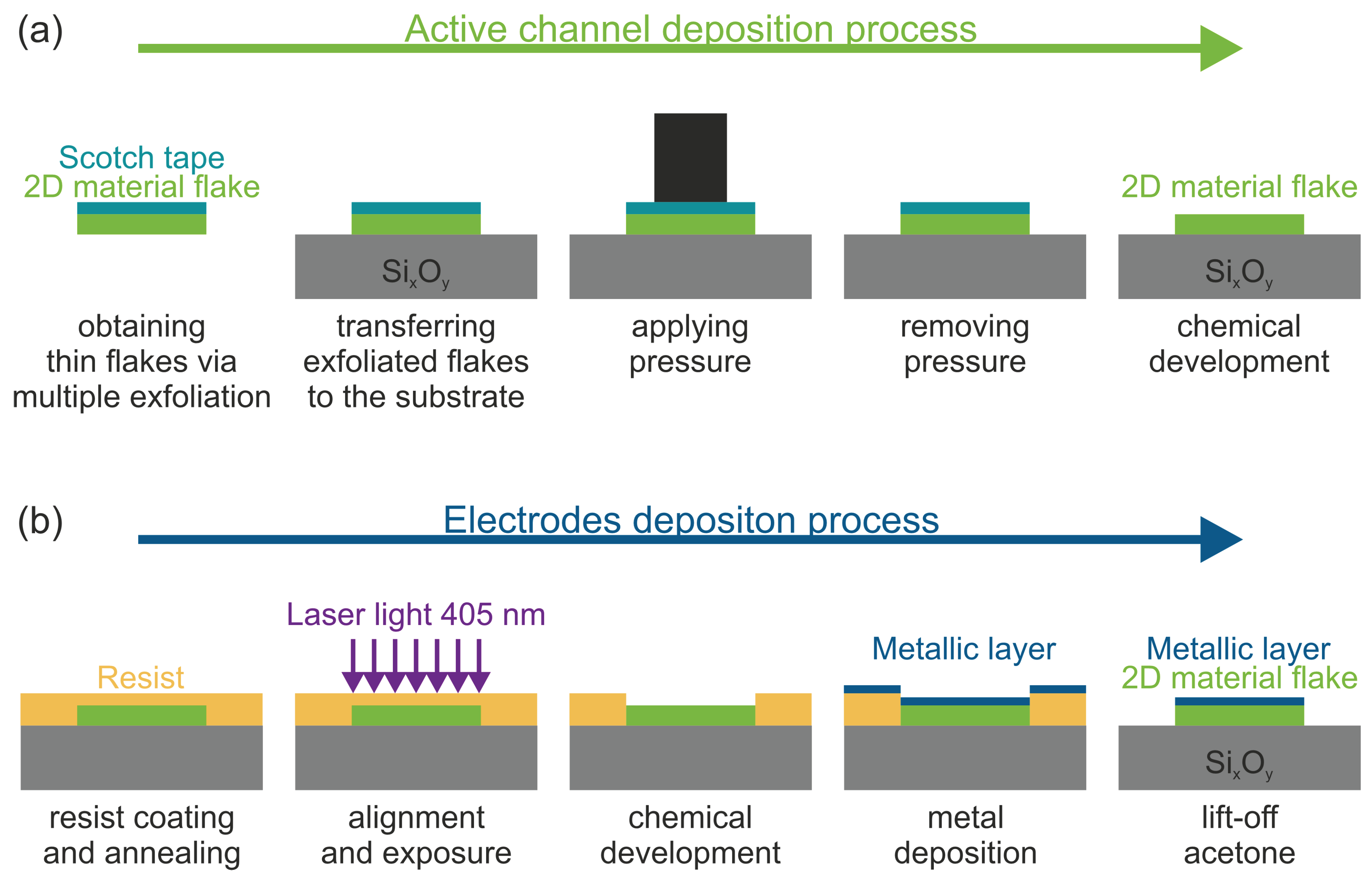
Figure 2.
Representative layered materials-based hybrid on-bottom structures, fabricated using SSP: a) Hall structure on Bi2Se3 flake, b) star-shaped electrode structure on HfSe2 flake.
Figure 2.
Representative layered materials-based hybrid on-bottom structures, fabricated using SSP: a) Hall structure on Bi2Se3 flake, b) star-shaped electrode structure on HfSe2 flake.
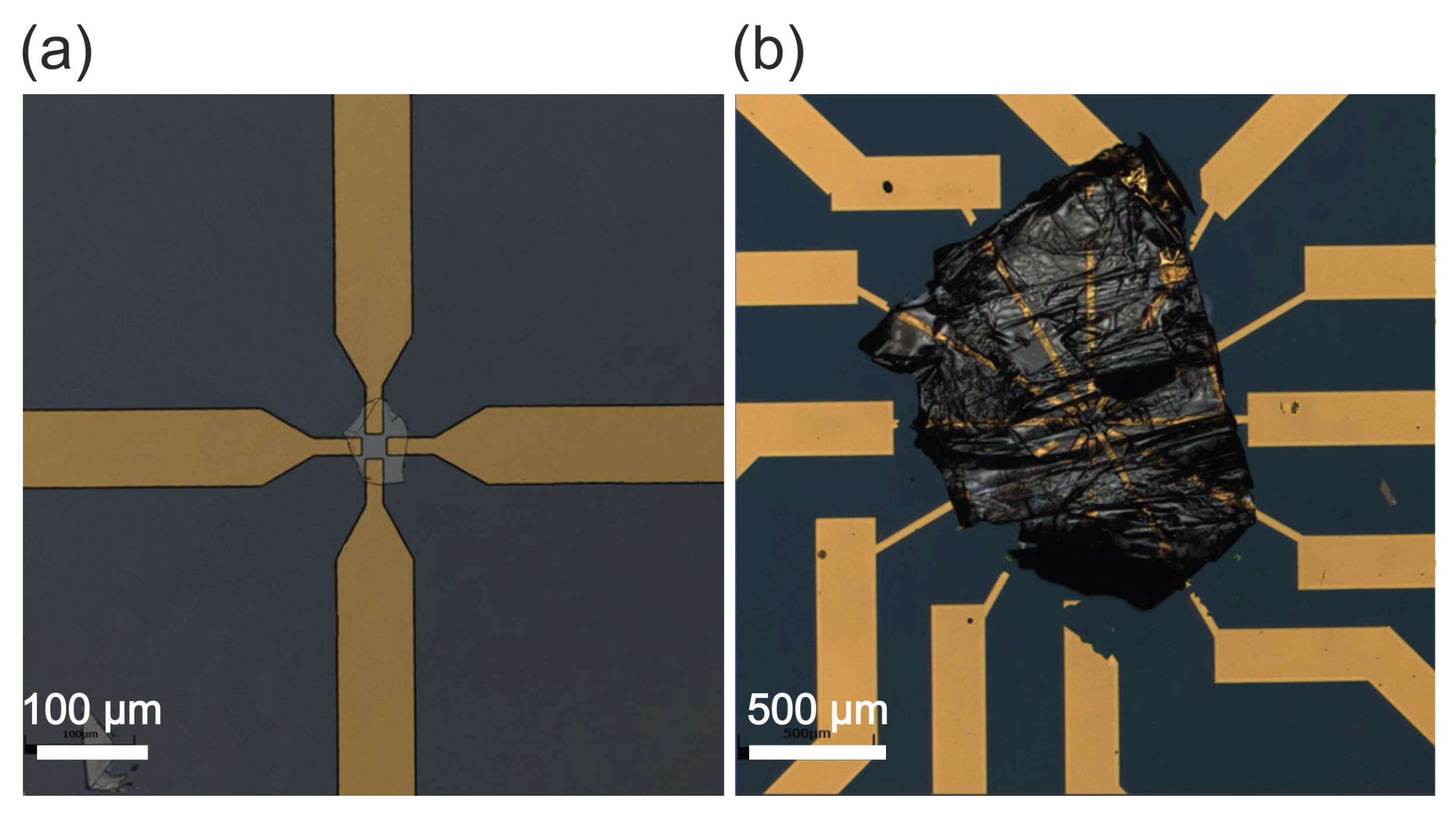
Figure 3.
Schematic presentation of the reversed structuring procedure using an exfoliated flake as an on-top active channel in the device. Detailed description in the manuscript text.
Figure 3.
Schematic presentation of the reversed structuring procedure using an exfoliated flake as an on-top active channel in the device. Detailed description in the manuscript text.
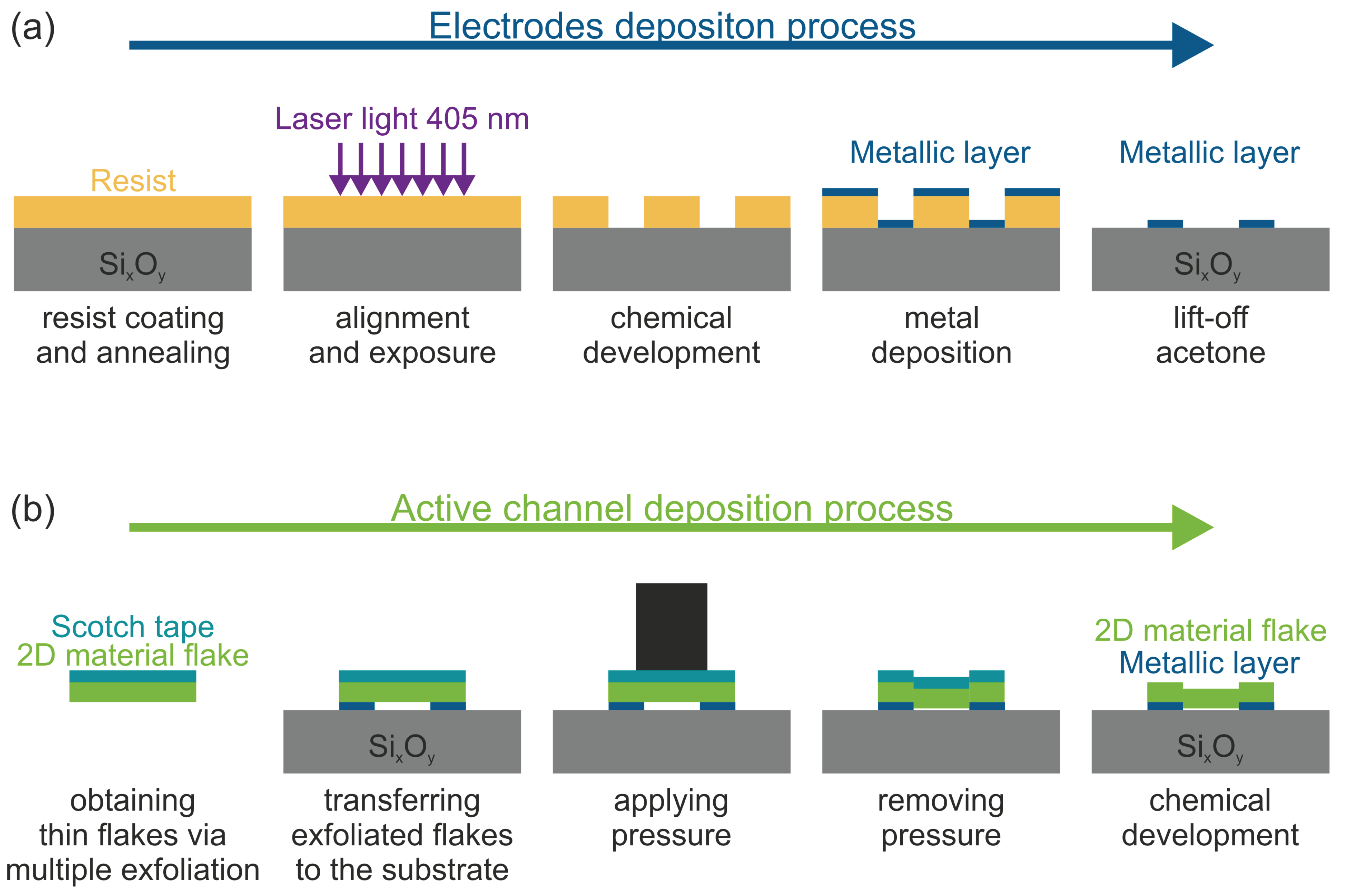
Figure 4.
Representative layered materials-based hybrid structures on-top fabricated using RSP: a) full-scale top-view image of SSES with deposited B2Se3 flake (electrodes pads at the corner allow for the use of needle measuring contacts); the labeling notation of the contacts is included; b) magnified image of the B2Se3 flake deposited on the SSES; c) magnified image of the HfSe2 flake deposited on the SSES.
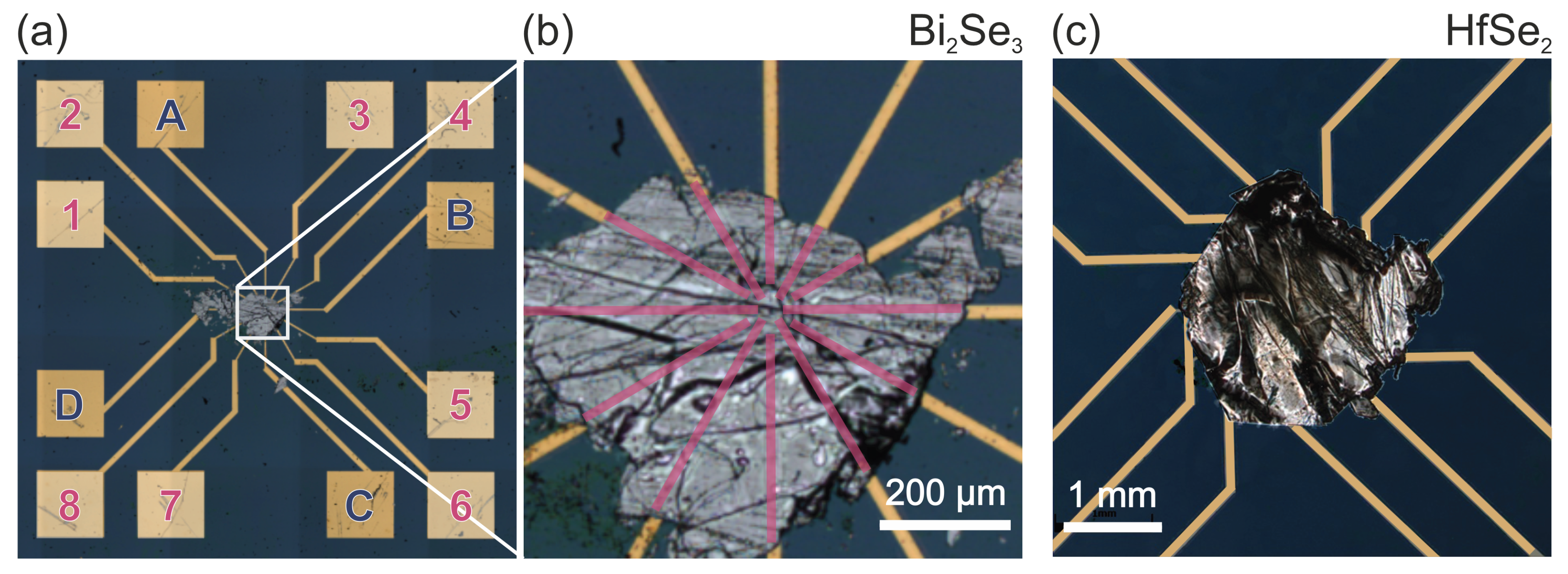
Figure 5.
Representative experimental dependencies of the gMR values as a function of magnetic field induction for the Bi2Se3 SSES device at defined configurations of the connections. The connection configurations correspond to the notation given in Figure 4a.
Figure 5.
Representative experimental dependencies of the gMR values as a function of magnetic field induction for the Bi2Se3 SSES device at defined configurations of the connections. The connection configurations correspond to the notation given in Figure 4a.
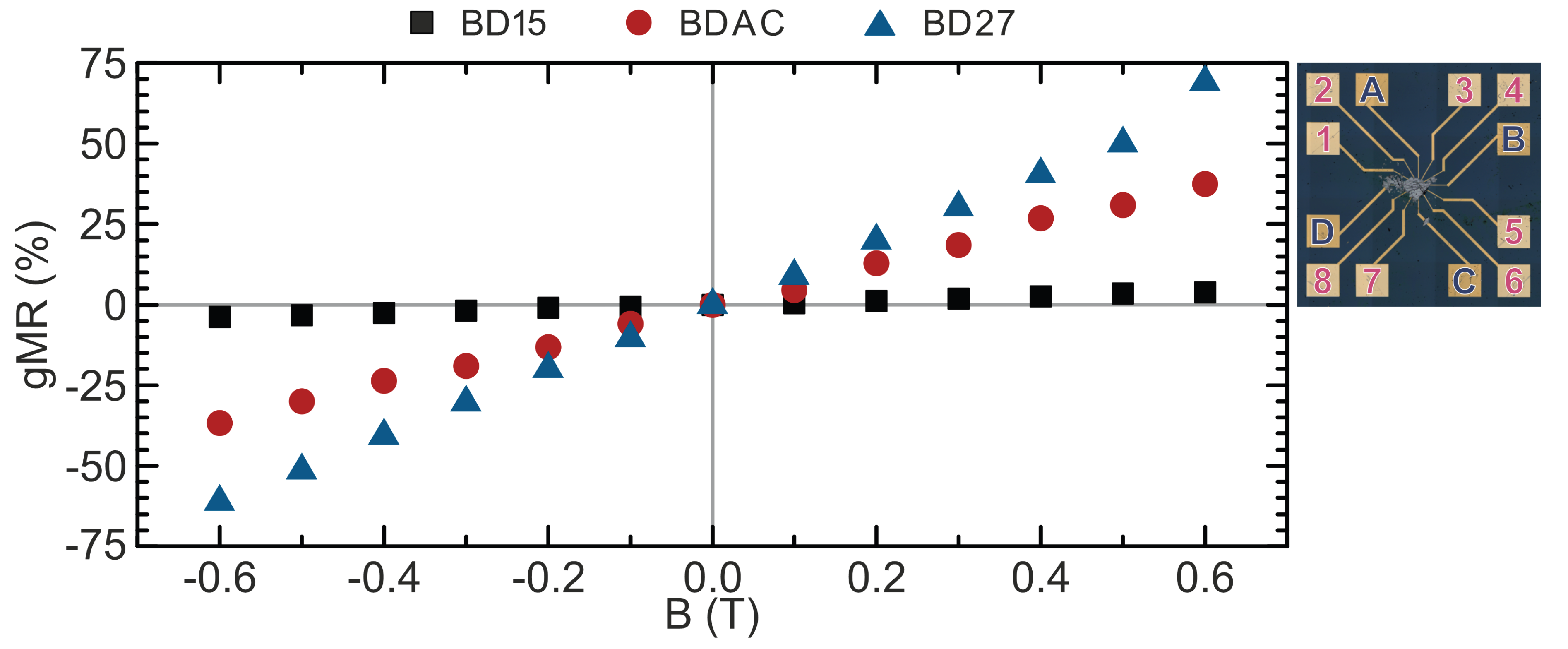

Table 1.
Determined materials parameters (charge carrier mobility ( ) and sheet charge concentration ()) for hybrid structures fabricated using SSP and RSP for Bi2Se3 and HfSe2 flakes.
Table 1.
Determined materials parameters (charge carrier mobility ( ) and sheet charge concentration ()) for hybrid structures fabricated using SSP and RSP for Bi2Se3 and HfSe2 flakes.
| Structure | (cm2/(V s)) | (1/cm2) |
|---|---|---|
| Bi2Se3 SSP | 60 | |
| Bi2Se3 RSP | 720 | |
| HfSe2 SSP | 20 | |
| HfSe2 RSP | 60 |
Disclaimer/Publisher’s Note: The statements, opinions and data contained in all publications are solely those of the individual author(s) and contributor(s) and not of MDPI and/or the editor(s). MDPI and/or the editor(s) disclaim responsibility for any injury to people or property resulting from any ideas, methods, instructions or products referred to in the content. |
© 2025 by the authors. Licensee MDPI, Basel, Switzerland. This article is an open access article distributed under the terms and conditions of the Creative Commons Attribution (CC BY) license (http://creativecommons.org/licenses/by/4.0/).
Copyright: This open access article is published under a Creative Commons CC BY 4.0 license, which permit the free download, distribution, and reuse, provided that the author and preprint are cited in any reuse.


