
Submitted:
25 June 2025
Posted:
26 June 2025
You are already at the latest version
Abstract
Two-dimensional (2D) intrinsic half-metal materials facilitate spin filtering, low-energy dissipation, and enhanced signal integrity, making them highly desirable for next-generation nanoelectronics and quantum technologies. In this work, we constructed two novel 2D half-metallic materials, α₁-ScSi₂N₄, and α₂-ScSi₂N₄, with unconventional ferromagnetism originating from N atoms rather than the transition metal Sc. First-principles calculations confirm their dynamic and thermal stability, as well as their intrinsic half-metallicity. We further demonstrate that their electronic and optical properties can be effectively tuned via strain, atomic adsorption, and external electric fields. A half-metal-to-metal transition occurs under compressive strain (α₁: 10%; α₂: 6-10%), while H/F adsorption induces a metallic state in α₁, and H adsorption does so in α₂. Furthermore, α₁ becomes metallic at electric fields of -0.2 to -0.5 V/Å and 0.2 to 0.5 V/Å, while α₂ undergoes a similar transition at electric fields of -0.3 to -0.5 V/Å and 0.3 to 0.5 V/Å. Both materials exhibit strong deep-UV absorption, indicating potential in optoelectronics. Symmetry breaking, charge transfer and energy level shifting maybe the tunability mechanisms caused the half-metal-to-metal transition. These findings not only expand the family of 2D half-metals with non-metal-derived magnetism but also provide new avenues for designing tunable magnetic materials for reconfigurable electronic, spintronic, and photonic applications.
Keywords:
intrinsic halfmetallicity
; 2D MA2Z4 materials
; non-metal-induced ferromagnetism
; first-principles calculations
1. Introduction
Two-dimensional (2D) materials have attracted widespread interest due to their exceptional electronic, mechanical, and thermal properties. These materials exhibit high carrier mobility [1], large on/off ratios [2], excellent thermal conductivity [3], and outstanding mechanical strength [4], making them highly promising for future technological advancements. However, most stable 2D materials, such as graphene [5], hexagonal boron nitride (h-BN) [6], and molybdenum disulfide (MoS₂) [7], are intrinsically non-magnetic, which limits their applications in magnetism-related fields.
Among magnetism-related 2D materials, half-metals stand out due to their unique electronic and spin-polarized properties, making them highly valuable for applications in data storage, magnetic field sensing, and spintronic devices. [8]Half-metals exhibit characteristics of both metals and semiconductors, behaving as a metal in one spin channel while acting as a semiconductor or insulator in the other. Their ability to provide 100% spin-polarized current makes them ideal for high-efficiency spintronic applications. [9] Moreover, their atomic-scale thickness enables ultra-compact device integration, while their 2D morphology allows precise external control. However, most pristine 2D materials are either nonmagnetic or lack intrinsic half-metallicity. Even when half-metallicity is present, the band gap is often too small to meet the essential requirements for spintronic applications. [10]These limitations have driven researchers to explore novel 2D magnetic materials through bottom-up design approaches, seeking optimal properties for next-generation spintronic devices.
Numerous studies have investigated the intrinsic properties of half-metals [11], exploring their topological characteristics [12], quantum transport phenomena [13], as well as their potential applications in nanoelectronics [14] and spintronics [15]. Extensive studies have demonstrated that strain engineering, chemical doping, and heterojunction construction represent effective approaches for modulating these materials’ electronic structure and magnetic characteristics. [16,17,18,19] However, the underlying mechanisms governing electronic phase transitions in half-metals remain largely unexplored. This raises a fundamental question: Can a half-metal be transformed into a metallic state through external perturbations, and what mechanisms drive this transition?
From a theoretical perspective, electronic phase transitions in 2D half-metals involve key mechanisms such as band overlap [20], Fermi level shifting [21], charge transfer [22], and symmetry breaking [23]. Understanding these processes advances knowledge in band engineering, electron correlation, and quantum phase transitions in low-dimensional materials. Additionally, controlling the electronic structure of half-metals could lead to topological phase transitions, potentially unlocking novel quantum states relevant to quantum computing and spintronics. [24]On the application side, the ability to induce a metallic state in half-metals opens up possibilities for reconfigurable electronic devices, low-power field-effect transistors, and phase-change memory. [25] Furthermore, their tunable conductivity makes them promising candidates for transparent conducting films [26], plasmonic materials, and optoelectronic applications [27].
In 2020, Hong et al. successfully synthesized monolayer MoSi₂N₄, a representative member of the MA₂Z₄ family, via chemical vapor deposition (CVD). [28]This material exhibited remarkable environmental stability, excellent mechanical strength, and strong optical absorption capability. [29] Inspired by this advancement, we constructed a novel monolayer structure of ScSi₂N₄ through a rational elemental substitution approach. Compared with the previously reported α₁-phase and related heterostructures [30,31,32], we identified an energetically favorable new structural phase, referred to as the α₂-ScSi₂N₄ phase. A comprehensive theoretical investigation was subsequently conducted on both α₁- and α₂-ScSi₂N₄, focusing on their electronic structures, optical responses, and magnetic properties. The results provide valuable insights into the structure-property relationships in this emerging class of two-dimensional materials.
In this work, we systematically investigate the stability, magnetic properties, and tunable electronic and optical characteristics of 2D α₁-ScSi₂N₄ and α₂-ScSi₂N₄ using first-principles density functional theory (DFT) calculations. The structural stability of both phases is verified through phonon spectrum analysis and molecular dynamics simulations. Our results confirm that α₁-ScSi₂N₄ and α₂-ScSi₂N₄ exhibit halfmetallic behavior, with metallic conductivity in the spin-down channel and semiconducting behavior in the spin-up channel. By constructing different magnetic configurations, we identify ferromagnetism as the magnetic ground state and reveal that the magnetism primarily originates from nitrogen atoms. This discovery, where magnetism arises from non-transition metal elements, provides new theoretical insights into magnetic 2D materials.
Furthermore, we demonstrate that both α₁-ScSi₂N₄ and α₂-ScSi₂N₄ undergo a transition from half-metallicity to metallicity under three distinct external perturbations: atomic adsorption, strain engineering, and electric field application. In the α₁-ScSi₂N₄ system, a compressive strain of 10% induces a half-metal-to-metal transition, whereas α₂-ScSi₂N₄ exhibits a similar transition under 6%-10% compressive strain. Additionally, the half-metallicity of α₁-ScSi₂N₄ disappears upon the adsorption of H or F atoms, while α₂-ScSi₂N₄ undergoes a comparable transition upon H adsorption. Under the action of an external electric field, when the field strength is -0.2 to -0.5 V/Å and 0.2 to 0.5 V/Å, α₁-ScSi₂N₄ transforms into a metallic state; when the field strength is -0.3 to -0.5 V/Å and 0.3 to 0.5 V/Å, α₂-ScSi₂N₄ becomes a metallic state. Our analysis reveals that charge transfer, symmetry breaking, and the Stark effect play crucial roles in these electronic transitions, offering new insights into phase changes in 2D half-metals.
Finally, we explore the optical properties of these materials and find that both α₁-ScSi₂N₄ and α₂-ScSi₂N₄ exhibit strong absorption peaks in the deep ultraviolet region, indicating their potential for photodetection applications. These findings highlight ScSi₂N₄ as a highly tunable material with promising applications in reconfigurable electronic and optoelectronic devices.
2. Computational Details
All structural optimizations and property evaluations were performed based on density functional theory (DFT) [33], as implemented in the Vienna Ab initio Simulation Package (VASP) [34]. The ion–electron interactions were described using the projector augmented-wave (PAW) method. [35] The exchange–correlation potential was treated with the generalized gradient approximation (GGA) [36] in the Perdew-Burke-Ernzerhof (PBE) formulation [37]. A plane-wave cutoff energy of 520 eV was adopted, and the electronic self-consistency was achieved with a total energy convergence threshold of 10-6 eV. Full relaxation was carried out until the Hellmann-Feynman force on each atom was less than 10-3 eV/Å.
To accurately simulate the monolayer structure, a vacuum spacing of ~30 Å was introduced along the out-of-plane (z) direction to suppress spurious interactions between periodic images. Phonon dispersion relations were calculated using the finite displacement method with a 2 × 2 × 1 supercell, as implemented in the PHONOPY package. [38] Additionally, first-principles molecular dynamics (FPMD) simulations were conducted on a 3 × 3 × 1 ScSi₂N₄ supercell within the canonical (NVT) ensemble at 300 K, with a time step of 2 fs and a total simulation duration of 8 ps. [39]
The VASPKIT utility [40] was employed for both preprocessing and postprocessing tasks. The frequency-dependent complex dielectric function ε(ω) was extracted from the dielectric tensor computed by VASP, and the optical absorption coefficient α(ω) was subsequently derived via the Kramers-Kronig transformation. The peak positions and intensities of α(ω) provide direct insight into the optical band gap and interband transition characteristics of the material.
3. Results and Discussion
3.1. Structure and Stability
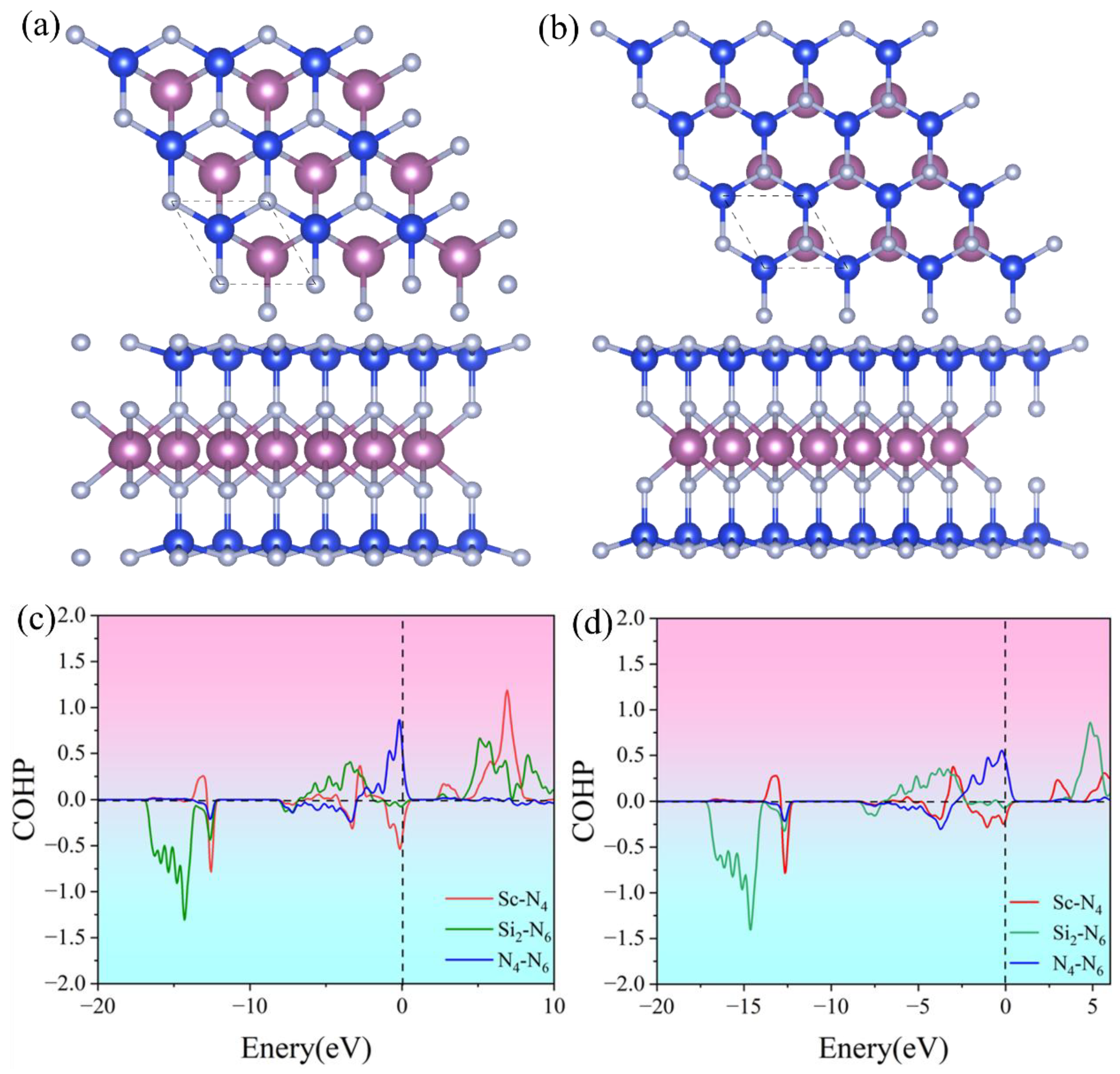
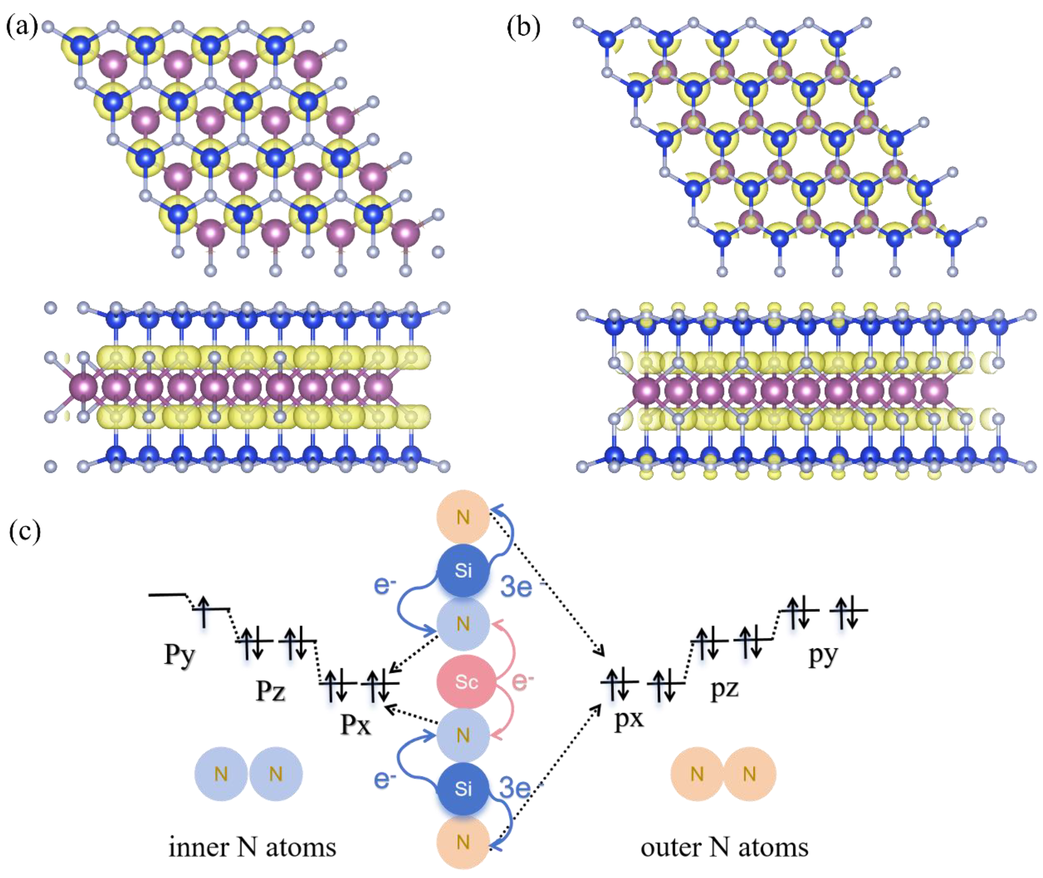
α1-ScSi₂N₄ and α2-ScSi₂N₄ phases belong to the emerging family of two-dimensional MA₂Z₄ materials, which consist of M-site (Group IVB, VB, or VIB elements), A-site (Group IVA), and Z-site (Group VA) atoms [Figure 1a,b]. These materials exhibit diverse electronic structure characteristics, spanning semiconductors, metals, insulators, and magnetic phases, rendering them promising for low-dimensional physics and device applications. [41,42,43,44,45,46] The α1-ScSi₂N₄ and α2-ScSi₂N₄ phases we constructed both adopt a quasi-hexagonal lattice, featuring a seven-layer atomic arrangement (N-Si-N-Sc-N-Si-N), where the Sc atomic layer is symmetrically embedded between Si–N layers, forming a stable sandwich-like monolayer structure. The ScN₂ layer resembles the structural motif of a MoS₂-type monolayer. Structural optimization reveals lattice constants of a = b = 2.97 Å (α₁) and a = b = 2.99 Å (α₂), both crystallizing in the space group (see Supplementary Table S1 for detailed structural parameters). Notably, the α₂ phase exhibits subtle differences in local atomic arrangement and interlayer coupling compared to the α₁ phase.
In the ScSi2N4 system, Sc and Si are sandwiched between different N layers. To analyze their bonding interactions, we calculated the crystal orbital Hamilton population (COHP). As shown in Figure 1c,d, the negative COHP value between Sc-N indicates that the Sc-N bond is in a bonding state and plays a skeletal support role in the structure. Si and N usually form strong covalent bonds. Si-N covalent bonds exist in nitride materials such as Si₃N [47], and electrons are filled in a lower energy range, which means that these bonds contribute to the structural stability of the material. Negative COHP values indicate that these N-N interactions are bonding and that they contribute to the crystal stability of the material. On the other hand, the charge density difference in Figure S1(a-b) clearly supports the formation of strong Si-N covalent bonds and Sc-N ionic bonds. This is further confirmed by Bader charge analysis [48] (As shown in Table S2). Each Sc atom transfers about 1e- to inner N atoms, and each Si transfers 1e- to inner N atoms and 3e- to outer N atoms, forming a polar covalent bond.
Figure 1.
Structures of (a) α1-ScSi2N4 and (b) α2-ScSi2N4, COHP diagrams of (c) α1-ScSi2N4 and (d) α2-ScSi2N4. Red, green, and blue represent the bonding between Sc and N, Si and N, and N and N, respectively.
Figure 1.
Structures of (a) α1-ScSi2N4 and (b) α2-ScSi2N4, COHP diagrams of (c) α1-ScSi2N4 and (d) α2-ScSi2N4. Red, green, and blue represent the bonding between Sc and N, Si and N, and N and N, respectively.
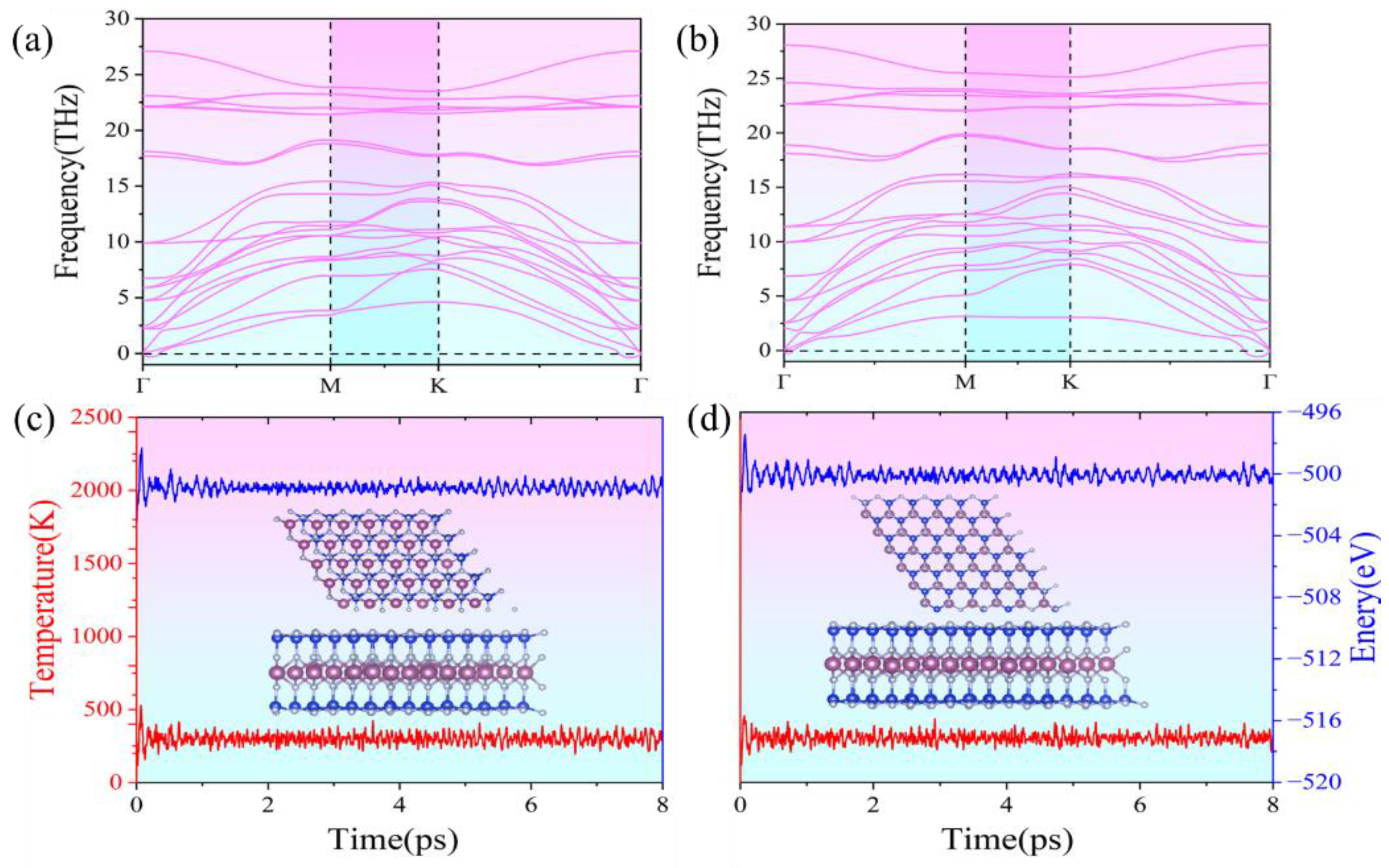
The stability of a compound is a crucial factor influencing its potential applications, as it directly impacts the feasibility of synthesis, device integration, and long-term operational reliability. Thermodynamic stability determines whether a material can be synthesized under practical conditions, while kinetic and mechanical stability ensure structural integrity under external perturbations such as temperature fluctuations and mechanical stress. Understanding these stability aspects aids in selecting appropriate synthesis routes, optimizing fabrication techniques, and predicting real-world performance in electronic, spintronic, and optoelectronic applications. Stability considerations include thermodynamic, kinetic, and mechanical aspects. The dynamic stability of ScSi2N4 was assessed using phonon dispersion calculations. As shown in Figure 2a,b, neither α1-ScSi2N4 nor α2-ScSi2N4 exhibits imaginary frequencies on all high-symmetry paths, which confirms their dynamic stability. In particular, the highest frequency (27-28 THz) of α1-ScSi2N4 and α2-ScSi2N4 structure indicates the robust connection between the Sc, Si, and N atoms in the two phases [49]. To further investigate the thermal stability of the ScSi2N4 monolayer, we performed AIMD simulations using a 2×2×1 supercell at 300 K. After 8 ps, slight atomic vibrations and well-converged energy were observed in the ab initio molecular dynamics (AIMD) results for both α1-ScSi2N4 and α2-ScSi2N4, demonstrating their thermodynamic stability. The absence of obvious structural distortions and bond breaking indicates the excellent thermal stability of the structure at 300K, as displayed in Figure 2c,d.
Figure 2.
Phonon spectra of (a) α1-ScSi2N4 and (b) α2-ScSi2N4, molecular dynamics of (c) α1-ScSi2N4 and (d) α2-ScSi2N4 at 300K for 8ps.
Figure 2.
Phonon spectra of (a) α1-ScSi2N4 and (b) α2-ScSi2N4, molecular dynamics of (c) α1-ScSi2N4 and (d) α2-ScSi2N4 at 300K for 8ps.
Cohesive energy is a key criterion for assessing the feasibility of material synthesis. A more negative cohesive energy indicates greater material stability. The cohesive energy of α1-ScSi2N4 is -7.706 eV/atom, and that of α2-ScSi2N4 is -7.714 eV/atom. The cohesive energy is close to that of C3N (-7.07 eV/atom) [50]and is comparable to the cohesive energy of the FeCN2 monolayer (-7.56 eV/atom) [51]. Mechanical stability has a certain impact on the synthesis of materials on substrates and determines the structural response under strain. The calculated elastic constants of α1-ScSi2N4 (i.e., C11=348.16N/m, C12=152.70N/m, C66=97.73N/m) and α2-ScSi2N4 (i.e., C11=333.00N/m, C12=130.72N/m, C66=101.14N/m) satisfy the Born stability criterion [52,53] for a Hexagonal system (i.e., C66>0, and C11>|C12|). The results indicate that they are mechanically stable, can maintain stability during the synthesis process, and their response under strain should be reliable. The Young’s modulus and Poisson’s ratio, which vary with angle, exhibit isotropy, as shown in Figure S2(a, c). The Young’s modulus for α1-ScSi2N4, reflecting the material’s flexibility/stiffness, is 281.19 N/m, while for α2-ScSi2N4, it is 281.67N/m. These values are much smaller than the 340 N/m of graphene [54], but larger than the 130 N/m of MoS2 [55], suggesting flexibility within the plane. In two-dimensional materials, the Poisson’s ratio (defined as the mechanical response to external strain) is 0.44 for α1-ScSi2N4 and 0.40 for α2-ScSi2N4, as shown in Figure S2(b, d). Overall, Young’s modulus and Poisson’s ratio show high structural flexibility, facilitating device preparation.
3.2. Electronic Behavior
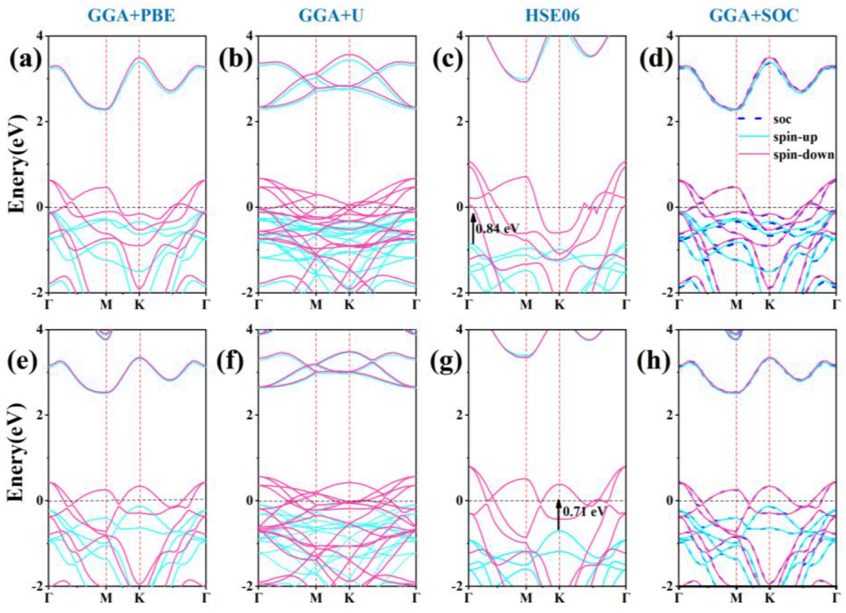
For two-dimensional materials, electronic properties are crucial as they determine the material’s nature and significantly influence its practical applications. The electronic band structure of α1-ScSi2N4 and α2-ScSi2N4 are calculated from GGA+PBE, GGA+U (U=1 eV [8]), HSE06, and GGA+SOC methods as shown in Figure 3. The high symmetry paths of the two structures are both along Γ–M–K–Γ. In the spin-down channel, the valence band crosses the Fermi level, indicating metallic properties. In the spin-up channel, the band gaps are 2.29 eV for α1-ScSi2N4 and 2.53 eV for α2-ScSi2N4 at the GGA+PBE level. And the band gap values in the spin-up channel are similar at GGA+PBE, GGA+U, and GGA+SOC methods (HSE06 band structure results show a relatively large spin-up band gap). Although the band positions calculated by different methods are offset, half-metallicity is significant and well preserved in both α1-ScSi2N4 and α2-ScSi2N4 at various calculation methods.
Half-metal has great application prospects in spintronic devices, but a wide half-metal energy gap is the key to achieving this property. We usually call the absolute minimum of CBM and VBM in the spin direction of the semiconductor the half-metal gap ( ). [56] The HSE06 band structure results further confirm that the α1 and α2-ScSi₂N₄ monolayers are intrinsically half-metal materials. According to this criterion, the equilibrium of the α1-ScSi2N4 monolayer is 0.84 eV, which is larger than YSi2N4 (0.248 eV) [56]. The equilibrium EHM of the α2-ScSi2N4 monolayer is 0.71 eV, which prevents spin flipping. These properties have significant implications for the electronic transport properties, thermoelectric performance, spintronic characteristics, and topological features of the materials. As the data using the PBE functional gives consistent qualitative analysis results, in the subsequent calculation, we use the GGA+PBE method for all calculations.
Figure 3.
Electronic band structure of (a-d, the upside line) α1-ScSi2N4 and (e-h, the downside line) α2-ScSi2N4 calculated from GGA+PBE, GGA+U, HSE06, and GGA+SOC methods.
Figure 3.
Electronic band structure of (a-d, the upside line) α1-ScSi2N4 and (e-h, the downside line) α2-ScSi2N4 calculated from GGA+PBE, GGA+U, HSE06, and GGA+SOC methods.
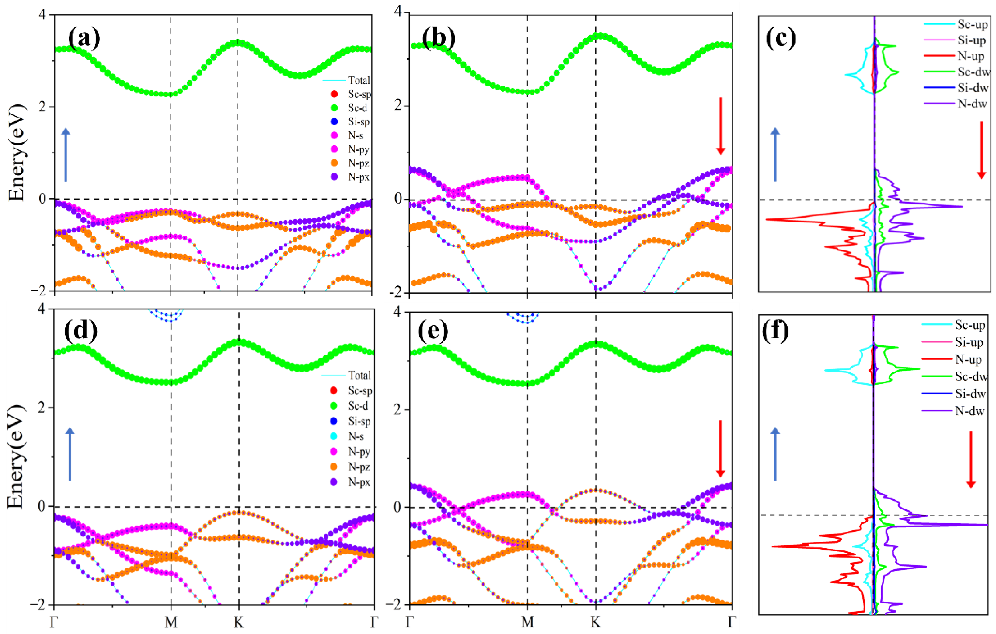
Understanding the origin of half-metallicity is essential for further exploration of the material’s magnetic and spintronic properties. To elucidate the underlying mechanism, we computed the orbital-resolved electronic band structures and spin-polarized density of states (DOS) for both α₁- and α₂-ScSi₂N₄ monolayers, as depicted in Figure 4. The results reveal that the electronic states near the Fermi level are primarily derived from N and Sc atoms. Specifically, in both phases, the spin-down components of N-p orbitals (px, py, and pz) intersect the Fermi level, whereas the corresponding spin-up orbitals lie entirely below it, indicating complete occupancy of spin-up states and partial occupancy of spin-down states.
For α₁-ScSi₂N₄, the conduction band minimum (CBM) in the spin-down channel is located at the M point and mainly originates from Sc-d orbitals, while the valence band maximum (VBM) appears at the Γ point and is dominated by N-px states. In α₂-ScSi₂N₄, the CBM remains at the M point with significant Sc-d character, whereas the VBM at the Γ point is primarily contributed by N-py orbitals. The spin-resolved DOS shown in Figure 4c,f further supports that the unpaired states at the Fermi level predominantly arise from the N-p orbitals, with negligible contributions from Sc and Si atoms.
These findings clearly demonstrate that the half-metallic behavior is chiefly governed by the spin asymmetry of nitrogen p orbitals, with spin-up states being fully occupied and spin-down states partially unoccupied. Moreover, the presence of spin-down band crossings at the Fermi level suggests a robust spin polarization, implying asymmetric electron distribution between spin channels. Such a feature confirms the half-metallic nature and provides a foundation for subsequent investigations into the magnetic characteristics of the ScSi₂N₄ monolayers.
Figure 4.
Orbital projection band structure and spin projection density of states (DOS) of α1-ScSi2N4 (a, b, c) and α2-ScSi2N4 (d, e, f). The ⬆ or ⬇ represents spin-up or spin-down, respectively.
Figure 4.
Orbital projection band structure and spin projection density of states (DOS) of α1-ScSi2N4 (a, b, c) and α2-ScSi2N4 (d, e, f). The ⬆ or ⬇ represents spin-up or spin-down, respectively.
3.3. Magnetic Properties
The unique electronic properties of ScSi2N4 monolayers inspired us to explore their magnetic properties. We established four magnetic state configurations to explore the magnetic ground state of α1-ScSi2N4 and α2-ScSi2N4. (As shown in the supporting information Figure S3), Calculations found that both α1-ScSi2N4 and α2-ScSi2N4 are ferromagnetic ground states. Surprisingly, the ferromagnetism in ScSi2N4 primarily originates from N atoms, rather than the transition metal Sc. In α1-ScSi2N4, the local magnetic moment of Sc is approximately 0.05μB, while two types of N atoms exhibit magnetic moments of 0.34 μB (type 1 N: near Sc atom) and 0.05 μB (type 2 N: far from Sc atom), respectively. The magnetic moment of Sc atoms in α2-ScSi2N4 is about 0.04 μB, the local magnetic moment of type 1 N atoms is about 0.3 μB, and the local magnetic moment of type 2 N atoms is 0.05 μB. These observations raise two key questions: (1) why does magnetism originate from non-metallic atoms, and (2) why do the N atoms in α1-ScSi2N4 and α2-ScSi2N4 exhibit different magnetic moments?
To gain deeper insight into the origin of magnetism, we analyzed the spin-orbit coupling (SOC) effect. If the bands near the Fermi level were primarily formed by the d orbitals of transition metal atoms, SOC would significantly alter these band structures, potentially introducing energy gaps, as seen in the 29 meV gap in the half-metallic VCl3 monolayer [57]. However, for the ScSi₂N₄ monolayer, since the bands near the Fermi level are mainly composed of the p orbitals of non-metallic N atoms, the SOC of the N-p orbitals is weaker than that of the TM-d orbitals. To verify this, we recalculated the electronic band structure using the GGA+SOC method (as shown in Figure 3d,h). The results show that the energy bands near the Fermi level are almost the same as those calculated by the GGA-PBE method. Since the GGA-PBE method cannot accurately describe the strongly correlated system containing unfilled d subshells, we used the GGA+U method to further verify the half-metallic properties of ScSi₂N₄ (see Figure 3b,f). The half-metallic properties of ScSi₂N₄ are well preserved except for a small shift in the energy band position. In addition, the magnetic moment calculation results show that the magnetic moment of each ScSi₂N₄ unit is about 1μB. These results prove that the magnetic moment is mainly contributed by the N-p orbital rather than the Sc-d orbitals.
We further examined the spin-polarized charge distribution (Figure 5a,b) and observed that the spin density is more delocalized in the intermediate region between the metal atoms, which is consistent with the magnetic moment properties in YN2 [58]. In conventional transition metal magnetic materials, the magnetic moment is mainly contributed by transition metal atoms. In ScSi₂N₄ monolayers, the Pauli electronegativity of N atoms (3.04) is much greater than the Pauli electronegativity of Sc atoms (about 1.36) and the electronegativity of Si (about 1.90). Therefore, Sc (3d¹4s²) and Si (3s²3p²) atoms will provide electrons to N (2s²2p³) atoms. Based on the Bader charge transfer analysis, each Sc atom transfers about one electron to adjacent N atoms. Each Si atom also transfers one electron to the N atoms adjacent to Sc. In short, both Sc and Si atoms transfer electrons to inner N atoms rather than outer N atoms. This results in the valence electrons of Sc atoms transferring to the N atoms, forming ionic bonds, Therefore, the Sc atom remains in the 3d²4s⁰ state, in which the two occupied 3d electrons are spin-antiparallel and exhibit a nearly zero magnetic moment.
This mechanism is analogous to the situation in TaN2 [59], where the strong electronegativity of N atoms destroys the magnetic ground state of metal atoms. Similarly, in TiC₂ [60],the electronic states near the Fermi level of transition metals are removed. At the same time, the 3p states of two inner N atoms share three foreign electrons, so that two N atoms carry nine 3p electrons. If we use the “nearly free electron gas” [61,62] model to describe these valence electrons, nine 3p electrons will present the electronic layer structure as shown in Figure 5c. This results in a magnetic moment of approximately 1μB per ScSi₂N₄ unit, which aligns with the results obtained using various methods, including GGA+PBE, GGA+U, and HSE06.
Figure 5.
(a) Spin charge density diagram of α1-ScSi2N4 and (b) α2-ScSi2N4. (c) Magnetic exchange mechanism diagram.
Figure 5.
(a) Spin charge density diagram of α1-ScSi2N4 and (b) α2-ScSi2N4. (c) Magnetic exchange mechanism diagram.
3.4. Optical Properties
As half-metals, α₁-ScSi₂N₄ and α₂-ScSi₂N₄ exhibit large band gaps in the spin-up direction, which contribute to their strong light absorption properties. As illustrated in Figure 6a,e, both phases display pronounced absorption peaks within the 0–200 nm range. This behavior is primarily attributed to their similarly large indirect band gaps in the spin-up channel, resulting in a low absorption coefficient in the visible light spectrum [63]. The half-metallicity of ScSi₂N₄ monolayers induces spin-polarized semiconducting behavior in the majority-spin channel, enabling optical transitions between the valence and conduction bands across this spectral range. These transitions correspond to fundamental bandgap excitations typical of semiconductors and insulators, or may involve intra-band excitations within the material’s molecular framework [64].
Moreover, the inherently wide bandgap of these materials enhances their resistance to strong light irradiation, making them highly suitable for ultraviolet (UV) applications. As shown in Figure 6, both α₁-ScSi₂N₄ and α₂-ScSi₂N₄ monolayers exhibit remarkable optical absorption in the deep ultraviolet (DUV, <200 nm) region, with absorption coefficients exceeding 3.2 × 10⁵ cm⁻¹, peaking in the 120-200 nm range. This material exhibits a pronounced absorption peak in the deep ultraviolet region, with an optical absorption capability comparable to that of other reported two-dimensional materials. For instance, monolayer MoS₂ [65]exhibits an absorption edge around 450 nm, with maximum UV absorption coefficients below 1.0 × 10⁵ cm⁻¹. The absorption intensity of α₁-and α₂-ScSi₂N₄ is also comparable to that of WSi₂N₄, which has a reported maximum absorption coefficient of 3.61 × 10⁵ cm⁻¹ [66].
Therefore, with their excellent deep-ultraviolet absorption capability, along with superior structural and thermal stability, α₁- and α₂-ScSi₂N₄ are promising candidates for next-generation high-performance ultraviolet optoelectronic devices, exhibiting performance comparable to some conventional two-dimensional materials in this field.
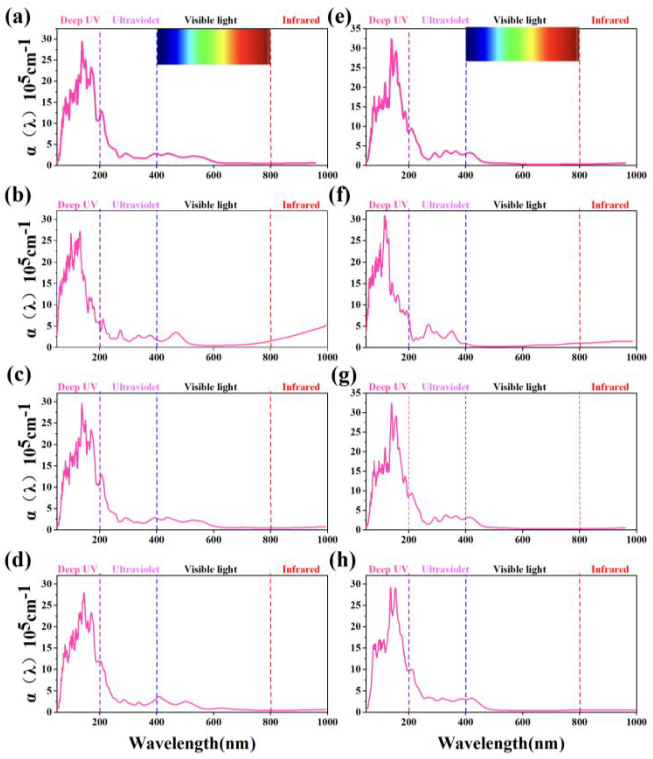
Figure 6.
Absorption spectra of (a-d, the left side row) α1-ScSi2N4 and (e-h, the right side row) α2-ScSi2N4 under different conditions. (a, e) Intrinsic monolayers, (b, f) under 10% biaxial compressive strain, (c, g) under an electric field of 5 V/A, (d, h) adsorbing an H atom.
Figure 6.
Absorption spectra of (a-d, the left side row) α1-ScSi2N4 and (e-h, the right side row) α2-ScSi2N4 under different conditions. (a, e) Intrinsic monolayers, (b, f) under 10% biaxial compressive strain, (c, g) under an electric field of 5 V/A, (d, h) adsorbing an H atom.
3.5. Regulation of Electronic and Optical Properties
Half-metals are a unique class of materials whose electronic structure exhibits characteristics of both metals and semiconductors. This distinctive electronic structure endows half-metals with numerous advantages, granting them broad application potential in fields such as electronics, spintronics, thermoelectric materials, and optical devices. To investigate the stability of half-metals, we employed methods such as strain, atomic adsorption, and external electric fields to modulate their half-metallic properties. These approaches effectively alter the band structure of the materials, enabling precise control over their electronic and optical properties and opening avenues for optimizing material performance.
3.5.1. Strain Effects
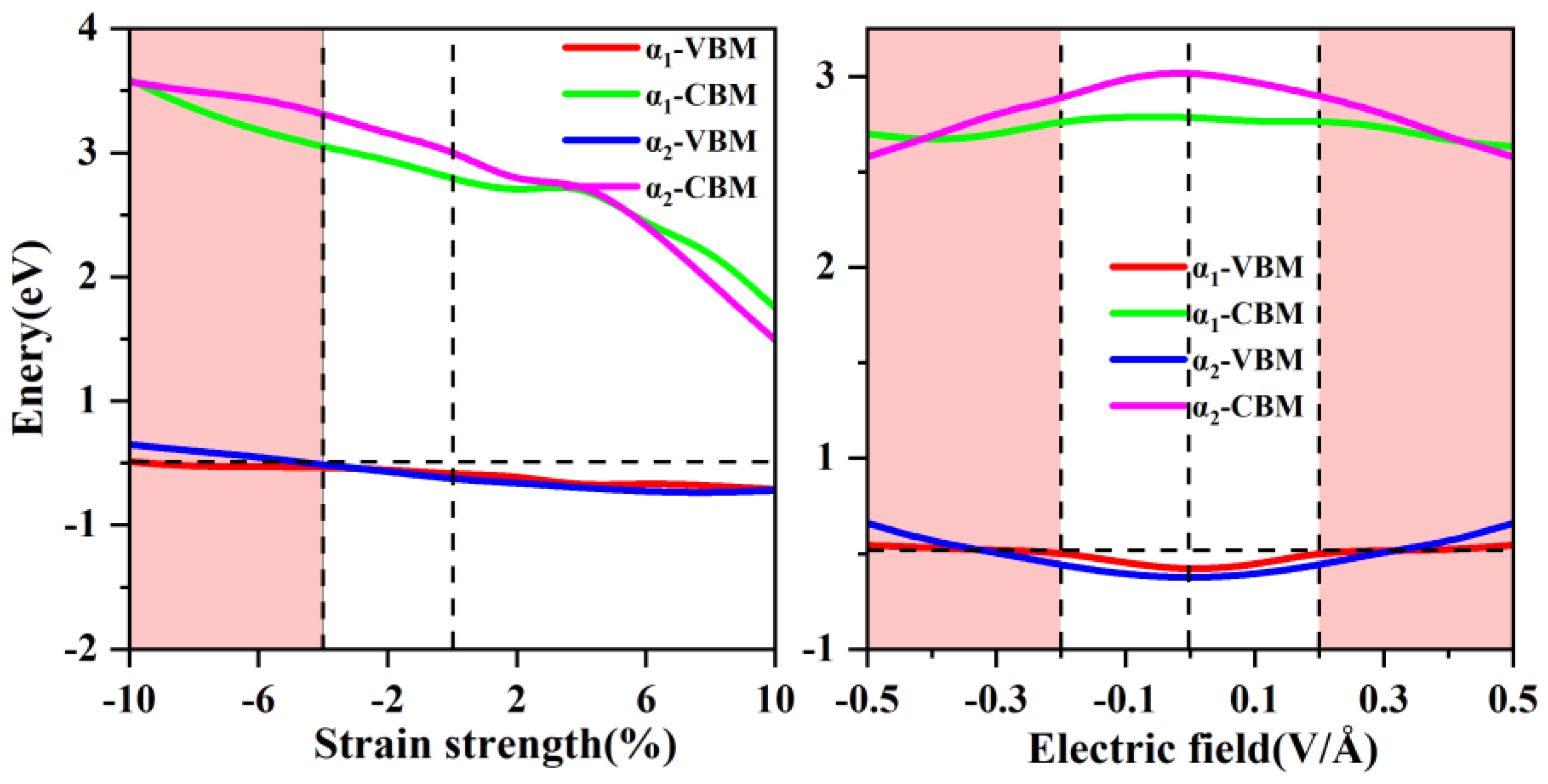
Strain engineering is a powerful technique for modulating the electronic [67], magnetic [68]and optical properties [66] of two-dimensional materials. Biaxial strain can be experimentally realized through thermal expansion mismatch [69]. In our calculations, we applied biaxial strain ranging from -10% to 10% to adjust the interatomic distances and analyzed its effects on the spin-up valence band maximum (VBM) and conduction band minimum (CBM) of α1-ScSi2N4 and α2-ScSi2N4, as shown in Figure 7a. For α1-ScSi2N4, a 10% compressive strain induces a transition to metallic behavior by causing the spin-up band to cross the Fermi level at the M point (see Figure S4, the blue circle indicates the half-metal to metal transition). Under tensile strain, the lattice expands, which can widen previously overlapping bands, leading to modifications in electronic band distribution. However, even under tensile strain, α1-ScSi2N4 retains its half-metallic nature (see Figure S4). In α2-ScSi2N4, a compressive strain in the range of 6%-10% induces a transition to metallicity, with the spin-up band crossing the Fermi level at the K point. (see Figure S5, the blue circle indicates the half-metal to metal transition) As tensile strain increases, α2-ScSi2N4 also retains its half-metallic properties, as confirmed in Figure S5.
Additionally, applying a 10% biaxial compressive strain modifies the optical properties of both α1-ScSi2N4 and α₂-ScSi₂N₄ (as depicted in Figure 6b,f); their primary absorption peaks remain and sharpen in the deep ultraviolet region. Interestingly, an additional peak emerges in the visible range of α1-ScSi2N4 under 10% compressive strain. These results indicate that strain can serve as an effective tuning parameter for regulating the electronic properties of ScSi2N4 monolayers, which is crucial for their application in high-performance electronic and optoelectronic devices.
Figure 7.
(a) The spin-up VBM and CBM of α1 and α2-ScSi2N4 vary with biaxial strain. (b) The band gap of α1 and α2-ScSi2N4 varies with increasing electric field strength.
Figure 7.
(a) The spin-up VBM and CBM of α1 and α2-ScSi2N4 vary with biaxial strain. (b) The band gap of α1 and α2-ScSi2N4 varies with increasing electric field strength.
3.5.2. Atoms Adsorption
Atomic or molecular adsorption is an effective strategy for modifying the physical properties of materials [63,64,70]. We examined the effects of adsorption on the physical properties of a ScSi2N4 monolayer based on a 2×2×1 supercell. During the adsorption of H, O, and F atoms on the ScSi2N4 supercell, four different adsorption sites were selected for structural optimization: the top of the N atom, the top of the Si atom, the Si-N bridge site, and the ring center position [71], as shown in Figure S6. By calculating the adsorption energy ( ), the most stable adsorption positions of atoms on the ScSi2N4 surface were determined.
Where represents the total energy of the adsorption system, is the energy of the pristine α1-ScSi2N4 or α2-ScSi2N4 monolayer, and is the energy of the isolated H, O, or F atom. Tables S3 and S4 list the total energies and adsorption energies of the ScSi2N4 monolayer at different adsorption sites. The results indicate that in the α1 system, H, O, and F atoms preferentially adsorb at the top of the N atom (a-site), with H-N, O-N, and F-N bond lengths of 1.10 Å, 1.60 Å, and 1.50 Å, respectively, representing the most stable configuration. In the α2-ScSi2N4 system, H and O atoms tend to adsorb at the top of the N atom (a-site), with H-N and O-N bond lengths of 1.10 Å and 1.60 Å, respectively, while the F atom prefers to adsorb at the top of the Si atom (b-site), with an F-Si bond length of 1.60 Å, forming the most stable configuration. Figure S7 presents the AIMD simulation results of H, O, and F atom adsorption on the α1-ScSi2N4 and α2-ScSi2N4 monolayers. No bond breaking, phase transitions, or significant structural distortions were observed during the simulation, confirming the excellent thermal stability of the atomic adsorption system at room temperature.
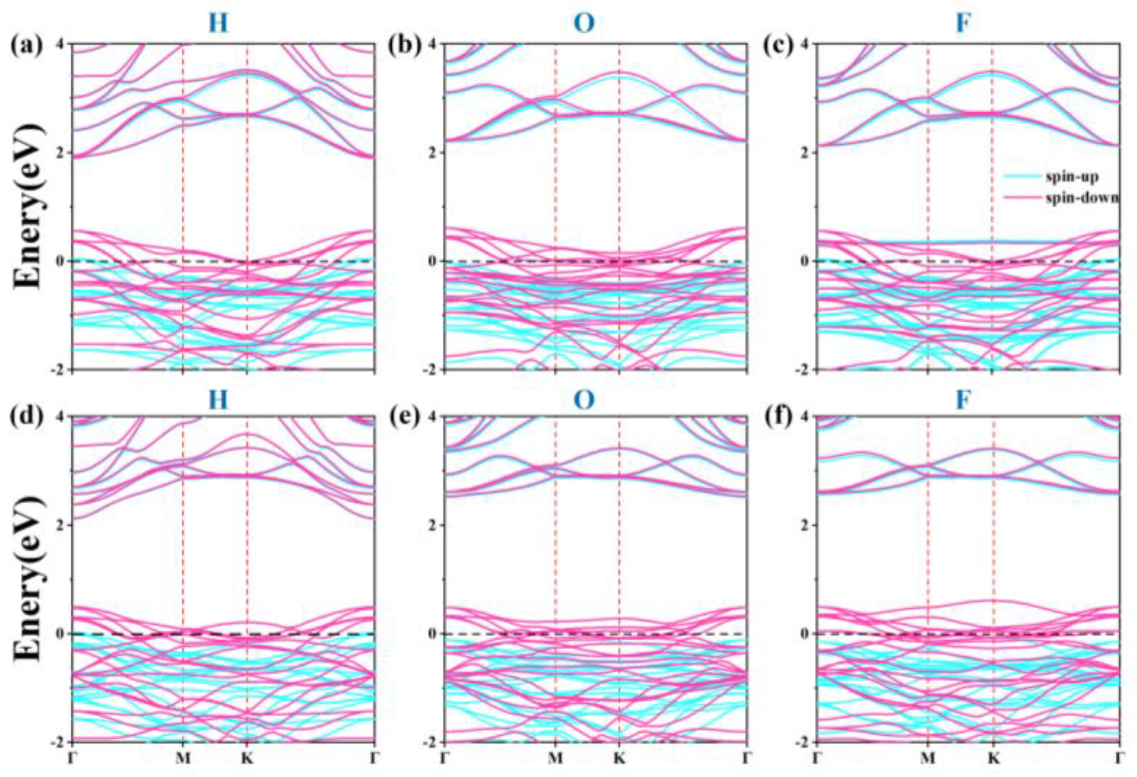
Subsequently, the electronic properties of hydrogen, oxygen, and fluorine atoms at their most stable adsorption sites were investigated. The electronic structures of the optimal adsorption sites were calculated, and the results are shown in Figure 8. It reveals that after the adsorption of H and F atoms, the half-metallic characteristics of the α1-ScSi2N4 monolayer disappear, transitioning to metallic properties. For the α2-ScSi2N4 monolayer, the electronic properties change from half-metallic to metallic only upon H atom adsorption.
Further calculations of the optical properties of the H atom adsorption system exhibits an absorption peak in the near-ultraviolet region, along with weak absorption peaks in the visible light region (blue and green light) (shown in Figure 6d,h). Tables S5 and S6 list total and partial magnetic moments of H, O, and F atoms adsorbed at the most stable site of α1-ScSi2N4 and α2-ScSi2N4 under adsorption conditions. The data show that the N atom remains the primary contributor to the total magnetic moment.
Figure 8.
Energy bands of (a-c) α1-ScSi2N4 and (d-f) α2-ScSi2N4 after adsorption of H, O, and F atoms.
Figure 8.
Energy bands of (a-c) α1-ScSi2N4 and (d-f) α2-ScSi2N4 after adsorption of H, O, and F atoms.
3.5.3. Electric Field Control
The electronic properties of 2D materials are also highly responsive to external electric fields [72,73,74]. We investigated the effects of applying an electric field along the z-direction, varying its strength from -0.5 to 0.5 V/Å. Electronic structure calculations (Figure 8b) indicate that increasing the electric field strength gradually reduces the spin-up band gap. When the electric field strength is -0.2 to -0.5 and 0.2 to 0.5, the spin-up conduction band at the Γ point moves down and crosses the Fermi level, which enhances the metallicity of α1-ScSi2N4. (As shown in Figure S8, the blue circle indicates the transition from half-metal to metal). In α2-ScSi2N4, the system maintains half-metallicity for field strengths in the range of -0.1 to -0.2 V/Å and 0.1 to 0.2 V/Å. However, for stronger fields (-0.3 to -0.5 V/Å or 0.3 to 0.5 V/Å), the spin-up valence band crosses the Fermi level at the K point, inducing a transition to metallic behavior. (As shown in Figure S9, the blue circle indicates the transition from half-metal to metal)
Additionally, the optical properties of α1-ScSi2N4 remain robust under an applied electric field, with its deep ultraviolet absorption peak intensifying as the field strength increases. Furthermore, a new absorption peak emerges in the visible region (Figure 6c). The optical response of α2-ScSi2N4 follows a similar trend, with increasing deep ultraviolet absorption intensity and the emergence of weak visible light absorption peaks (Figure 6g).
3.5.4. Mechanism of Regulating Electronic and Optical Properties
Half-metallic properties and optical properties of α1-ScSi2N4 and α2-ScSi2N4 are modulated under strain, atomic adsorption, and external electric fields. We thought that the mechanisms were different from the diverse regulating methods. The underlying mechanism for strain-induced property modulation is likely symmetry breaking, which alters electronic band structures and facilitates phase transitions. The primary mechanism driving the adsorption-induced modifications is mainly caused by charge transfer, which alters the electronic band structure and magnetic properties of the system. The dominant mechanism underlying electric-field-induced transitions is energy level shifting, where the applied field modulates charge distributions and band alignments, leading to phase transitions between half-metallic and metallic states. These findings highlight the potential of electric fields as a precise tuning parameter for controlling the electronic and optical properties of ScSi2N4 monolayers, paving the way for their application in reconfigurable spintronic and optoelectronic devices.
4. Conclusions
In this work, we calculated two novel 2D materials, α1-ScSi2N4 and α2-ScSi2N4 monolayers, and systematically investigated their structural stability, electronic properties, magnetic origin, and tunability under external perturbations. Phonon dispersion and ab initio molecular dynamics calculations confirm that both structures are dynamically and thermally stable. Our results reveal that α1-ScSi2N4 and α2-ScSi2N4 exhibit intrinsic half-metallicity, where the half-metallic behavior is predominantly governed by N-p orbitals rather than the transition metal Sc, highlighting an unconventional origin of magnetism in these materials. Furthermore, we explore the tunability of their electronic and optical properties under strain, atomic adsorption, and external electric fields. In the α1-ScSi2N4 system, a half-metal-to-metal transition occurs under a compressive strain of 10%, while α2-ScSi2N4 exhibits a similar transition within a 6%-10% strain range. Atomic adsorption studies show that H and F adsorption eliminate the half-metallicity of α1-ScSi2N4, leading to a metallic state, whereas in α2-ScSi2N4, only H adsorption induces a transition to metallic behavior. Under an applied electric field, α1-ScSi2N4 transforms from a half-metal to metal at -0.2 to -0.5 V/Å and 0.2 to 0.5 V/Å, while when subjected to an electric field strength of -0.3 to -0.5 V/Å or 0.3 to 0.5 V/Å, α2-ScSi2N4 exhibits metallic behavior. These tunability mechanisms (symmetry breaking, charge transfer, and energy level shifting) provide new insights into electronic phase transitions in 2D half-metals. Additionally, optical absorption calculations reveal that both α1-ScSi2N4 and α2-ScSi2N4 exhibit strong absorption peaks in the deep ultraviolet region, suggesting potential applications in photodetectors. Our findings not only expand the family of 2D half-metals with unconventional magnetic origins but also establish ScSi2N4 monolayers as promising candidates for reconfigurable spintronic, electronic, and optoelectronic devices.
Supplementary Materials
The following supporting information can be downloaded at the website of this paper posted on Preprints.org.
Data Availability Statement
The data that support the findings of this study are available from the corresponding author upon reasonable request.
Acknowledgments
This work was supported by the National Natural Science Foundation of China (No. 12204194) and the Program for the Development of Science and Technology of Jilin Province (No.20250101059JJ).
Conflicts of Interest
The authors declare no competing financial interest.
References
- Kou, L.; Frauenheim, T.; Chen, C. Phosphorene as a Superior Gas Sensor: Selective Adsorption and Distinct I – V Response. J Phys Chem Lett 2014, 5, 2675–2681. [CrossRef]
- Das, S.; Zhang, W.; Demarteau, M.; Hoffmann, A.; Dubey, M.; Roelofs, A. Tunable Transport Gap in Phosphorene. Nano Lett 2014, 14, 5733–5739. [CrossRef]
- Balandin, A.A.; Ghosh, S.; Bao, W.; Calizo, I.; Teweldebrhan, D.; Miao, F.; Lau, C.N. Superior Thermal Conductivity of Single-Layer Graphene. Nano Lett 2008, 8, 902–907. [CrossRef]
- King, A.; Johnson, G.; Engelberg, D.; Ludwig, W.; Marrow, J. Observations of Intergranular Stress Corrosion Cracking in a Grain-Mapped Polycrystal. Science (1979) 2008, 321, 382–385. [CrossRef]
- Geim, A. K.; Novoselov, K.S. The Rise of Graphene. Nat Mater 2007, 6, 183–191. [CrossRef]
- Pacilé, D.; Meyer, J.C.; Girit, Ç.Ö.; Zettl, A. The Two-Dimensional Phase of Boron Nitride: Few-Atomic-Layer Sheets and Suspended Membranes. Appl Phys Lett 2008, 92, 133107. [CrossRef]
- Yadav, V.K.; Mir, S.H.; Singh, J.K. A Computational Study of Structural, Electronic and Carrier Mobility of Boron and Phosphorus/Nitrogen Co-Doped Graphene. Physica B Condens Matter 2019, 571, 291–295. [CrossRef]
- Jiang, X.; Liu, Q.; Xing, J.; Liu, N.; Guo, Y.; Liu, Z.; Zhao, J. Recent Progress on 2D Magnets: Fundamental Mechanism, Structural Design and Modification. Appl Phys Rev 2021, 8, 31305. [CrossRef]
- Gupta, S.; Chakraborty, S.; Pakhira, S.; Barreteau, C.; Crivello, J.-C.; Bandyopadhyay, B.; Greneche, J.M.; Alleno, E.; Mazumdar, C. Coexisting Structural Disorder and Robust Spin-Polarization in Half-Metallic FeMnVAl. Phys Rev B 2022, 106, 115148. [CrossRef]
- Wu, Q.; Zhang, Y.; Zhou, Q.; Wang, J.; Zeng, X.C. Transition-Metal Dihydride Monolayers: A New Family of Two-Dimensional Ferromagnetic Materials with Intrinsic Room-Temperature Half-Metallicity. Journal of Physical Chemistry Letters 2018, 9, 4260–4266. [CrossRef]
- Zhu, M.X.; Ji, W.X.; Zhu, H.W.; Cao, Q.; Zhang, B.M. Symmetry-Protected Two-Dimensional Half-Semi-Metal NiVS6As2 Monolayer. J Electron Mater 2024, 53, 6250–6257. [CrossRef]
- Yan, B.; Felser, C. Topological Materials: Weyl Semimetals. Annu Rev Condens Matter Phys 2017, 8, 337–354. [CrossRef]
- Griffin, S.M.; Neaton, J.B. Prediction of a New Class of Half-Metallic Ferromagnets from First Principles. Phys Rev Mater 2017, 1, 044401. [CrossRef]
- Li, B.G.; Zheng, Y.F.; Cui, H.; Wang, P.; Zhou, T.W.; Wang, D.D.; Chen, H.; Yuan, H.K. First-Principles Investigation of a New 2D Magnetic Crystal: Ferromagnetic Ordering and Intrinsic Half-Metallicity. J Chem Phys 2020, 152, 244704. [CrossRef]
- Dihingia, K.D.; Saikia, S.; Yedukondalu, N.; Saha, S.; Sastry, G.N. 2D-Double Transition Metal MXenes for Spintronics Applications: Surface Functionalization Induced Ferromagnetic Half-Metallic Complexes. J Mater Chem C Mater 2022, 10, 17886–17898. [CrossRef]
- Tao, W.-L.; Lan, J.-Q.; Hu, C.-E.; Chen, X.-R.; Geng, H.-Y. Biaxial Strain Tuned Electronic Structure, Lattice Thermal Conductivity and Thermoelectric Properties of MgI2 Monolayer. Mater Sci Semicond Process 2022, 148, 106791. [CrossRef]
- Qi, W.; Abdugopur, H.; Xu, W.; Gao, M.; Hushur, A.; Zhang, H. Pressure-Induced Phase Transition toward High Symmetry in Zero-Strain Li2TiO3. Physical Chemistry Chemical Physics 2023, 25, 14918–14927. [CrossRef]
- Wang, Y.; Li, A.; Cheng, C. Ultrathin Co(OH)2 Nanosheets@Nitrogen-Doped Carbon Arrays as Efficient Air Cathodes for Rechargeable–Air Batteries. Small 2021, 17, 2101720. [CrossRef]
- Huang, H.M.; Cao, M.L.; Jiang, Z.Y.; Xiong, Y.C.; Zhang, X.; Luo, S.J.; Laref, A. High Spin Polarization in Formamidinium Transition Metal Iodides: First Principles Prediction of Novel Half-Metals and Spin Gapless Semiconductors. Physical Chemistry Chemical Physics 2019, 21, 16213–16222. [CrossRef]
- Maymoun, M.; Oukahou, S.; Bahou, Y.; Hasnaoui, A.; Sbiaai, K. Strain- and Electric Field-Enhanced Optical Properties of the Penta-Siligraphene Monolayer. New Journal of Chemistry 2022, 46, 13905–13917. [CrossRef]
- Huang, L.; Li, J. Tunable Electronic Structure of Black Phosphorus/Blue Phosphorus van Der Waals p-n Heterostructure. Appl Phys Lett 2016, 108, 083101. [CrossRef]
- Wu, Q.; Cao, L.; Ang, Y.S.; Ang, L.K. Semiconductor-to-Metal Transition in Bilayer MoSi2N4 and WSi2N4 with Strain and Electric Field. Appl Phys Lett 2021, 118, 1–5. [CrossRef]
- Friák, M.; Schindlmayr, A.; Scheffler, M. Ab Initio Study of the Half-Metal to Metal Transition in Strained Magnetite. New J Phys 2007, 9, 5–5. [CrossRef]
- Nayak, A.P.; Bhattacharyya, S.; Zhu, J.; Liu, J.; Wu, X.; Pandey, T.; Jin, C.; Singh, A.K.; Akinwande, D.; Lin, J.-F. Pressure-Induced Semiconducting to Metallic Transition in Multilayered Molybdenum Disulphide. Nat Commun 2014, 5, 3731. [CrossRef]
- Bafekry, A.; Faraji, M.; Fadlallah, M.M.; Bagheri Khatibani, A.; abdolahzadeh Ziabari, A.; Ghergherehchi, M.; Nedaei, Sh.; Shayesteh, S.F.; Gogova, D. Tunable Electronic and Magnetic Properties of MoSi2N4 Monolayer via Vacancy Defects, Atomic Adsorption and Atomic Doping. Appl Surf Sci 2021, 559, 149862. [CrossRef]
- Siwal, S.S.; Saini, A.K.; Rarotra, S.; Zhang, Q.; Thakur, V.K. Recent Advancements in Transparent Carbon Nanotube Films: Chemistry and Imminent Challenges. J Nanostructure Chem 2021, 11, 93–130.
- Li, Y.; Liu, J.; Zhang, P.; Jing, Q.; Liu, X.; Zhang, J.; Xiao, N.; Yu, L.; Niu, P. Electrical Transport Properties of EuTe under High Pressure. J Mater Chem C Mater 2021, 9, 17371–17381. [CrossRef]
- Hong, Y.-L.; Liu, Z.; Wang, L.; Zhou, T.; Ma, W.; Xu, C.; Feng, S.; Chen, L.; Chen, M.-L.; Sun, D.-M.; et al. Chemical Vapor Deposition of Layered Two-Dimensional MoSi2N4 Materials. Science (1979) 2020, 369, 670–674. [CrossRef]
- Mortazavi, B.; Javvaji, B.; Shojaei, F.; Rabczuk, T.; Shapeev, A. V; Zhuang, X. Exceptional Piezoelectricity, High Thermal Conductivity and Stiffness and Promising Photocatalysis in Two-Dimensional MoSi2N4 Family Confirmed by First-Principles;
- Pedroza-Rojas, B.; Sanchez-Castillo, A.; Ponce-Pérez, R. Structural, Electronic, and Magnetic Properties of the van Der Waals ScSi2N4/VSi2N4 Heterostructure: A First-Principles Study. ACS Omega 2025. [CrossRef]
- Huang, H.; Zhao, W.; Yang, M.; Xue, S.; He, Z.; Laref, A. Half-Metallic Behavior and Anisotropy of Two-Dimensional MoSi2N4/ScSi2N4 Heterojunction. J Magn Magn Mater 2024, 610. [CrossRef]
- Zhao, Z.; Wang, X.; Mi, W. Ferroelectric Polarization Tailored Spin Polarized Electronic Structure and Magnetic Anisotropy in Two-Dimensional ScSi2N4/CuInP2S6 Multiferroic Heterostructures. J Phys D Appl Phys 2023, 56. [CrossRef]
- Cohen, A.J.; Mori-Sánchez, P.; Yang, W. Challenges for Density Functional Theory. Chem Rev 2012, 112, 289–320. [CrossRef]
- Allouche, A.R. Gabedita - A Graphical User Interface for Computational Chemistry Softwares. J Comput Chem 2011, 32, 174–182. [CrossRef]
- Blöchl, P.E. Projector Augmented-Wave Method. Phys Rev B 1994, 50, 17953–17979. [CrossRef]
- Perdew, J.P.; Burke, K.; Ernzerhof, M. Generalized Gradient Approximation Made Simple. Phys Rev Lett 1996, 77, 3865–3868. [CrossRef]
- Paier, J.; Hirschl, R.; Marsman, M.; Kresse, G. The Perdew-Burke-Ernzerhof Exchange-Correlation Functional Applied to the G2-1 Test Set Using a Plane-Wave Basis Set. Journal of Chemical Physics 2005, 122. [CrossRef]
- Togo, A.; Tanaka, I. First Principles Phonon Calculations in Materials Science. Scr Mater 2015, 108, 1–5. [CrossRef]
- Martyna, G.J.; Klein, M.L.; Tuckerman, M. Nosé-Hoover Chains: The Canonical Ensemble via Continuous Dynamics. J Chem Phys 1992, 97, 2635–2643. [CrossRef]
- Wang, V.; Xu, N.; Liu, J.C.; Tang, G.; Geng, W.-T. VASPKIT: A User-Friendly Interface Facilitating High-Throughput Computing and Analysis Using VASP Code. 2019. [CrossRef]
- Wang, L.; Shi, Y.; Liu, M.; Zhang, A.; Hong, Y.-L.; Li, R.; Gao, Q.; Chen, M.; Ren, W.; Cheng, H.-M.; et al. Intercalated Architecture of MA2Z4 Family Layered van Der Waals Materials with Emerging Topological, Magnetic and Superconducting Properties. Nat Commun 2021, 12, 2361. [CrossRef]
- Li, S.; Wu, W.; Feng, X.; Guan, S.; Feng, W.; Yao, Y.; Yang, S.A. Valley-Dependent Properties of Monolayer MoSi2N4, WSi2N4 and MoSi2As4. Phys Rev B 2020, 102, 235435. [CrossRef]
- Bafekry, A.; Faraji, M.; Hoat, D.M.; Shahrokhi, M.; Fadlallah, M.M.; Shojaei, F.; Feghhi, S.A.H.; Ghergherehchi, M.; Gogova, D. MoSi2N4 Single-Layer: A Novel Two-Dimensional Material with Outstanding Mechanical, Thermal, Electronic, Optical, and Photocatalytic Properties. J Phys D Appl Phys 2021, 54, 155303. [CrossRef]
- Kang, L.; Lin, Z. Second Harmonic Generation of MoSi2N4 Layer. Phys Rev B 2021, 103, 195404. [CrossRef]
- Cao, L.; Zhou, G.; Wang, Q.; Ang, L.K.; Ang, Y.S. Two-Dimensional van Der Waals Electrical Contact to Monolayer MoSi2N4. Appl Phys Lett 2021, 118, 013106. [CrossRef]
- Yin, Y.; Gong, Q.; Yi, M.; Guo, W. Emerging Versatile Two-Dimensional MoSi2N4 Family. Adv Funct Mater 2023, 33, 2214050. [CrossRef]
- Wang, L.G.; Sun, J.X.; Yang, W.; Tian, R.G. Analytic Equation of State and Thermodynamic Properties for α-, β-, and γ-Si 3 N 4 Based on Analytic Mean Field Approach. Acta Phys Pol A 2008, 114, 807–818. [CrossRef]
- Bader, R.F.W. Atoms in Molecules. Acc Chem Res 1985, 18, 9–15. [CrossRef]
- Han, F.; Yan, X.; Li, F.; Yu, H.; Li, W.; Zhong, X.; Bergara, A.; Yang, G. Prediction of Monolayer FeP4 with Intrinsic Half-Metal Ferrimagnetism above Room Temperature. Phys Rev B 2023, 107, 024414. [CrossRef]
- Bai, K.; Cui, Z.; Li, E.; Ding, Y.; Zheng, J.; Liu, C.; Zheng, Y. Adsorption of Gas Molecules on Group III Atoms Adsorbed G-C3N4: A First-Principles Study. Vacuum 2020, 175, 109293. [CrossRef]
- Wang, Z.; Lou, H.; Han, F.; Yan, X.; Liu, Y.; Yang, G. An Antiferromagnetic Semiconducting FeCN2 Monolayer with a Large Magnetic Anisotropy and Strong Magnetic Coupling. Physical Chemistry Chemical Physics 2023, 25, 21521–21527. [CrossRef]
- Waller, I. Dynamical Theory of Crystal Lattices by M. Born and K. Huang. Acta Crystallogr 1956, 9, 837–838. [CrossRef]
- Zhang, S.; Zhou, J.; Wang, Q.; Chen, X.; Kawazoe, Y.; Jena, P. Penta-Graphene: A New Carbon Allotrope. Proc Natl Acad Sci U S A 2015, 112, 2372–2377. [CrossRef]
- Papageorgiou, D.G.; Kinloch, I.A.; Young, R.J. Mechanical Properties of Graphene and Graphene-Based Nanocomposites. Prog Mater Sci 2017, 90, 75–127.
- Cooper, R.C.; Lee, C.; Marianetti, C.A.; Wei, X.; Hone, J.; Kysar, J.W. Nonlinear Elastic Behavior of Two-Dimensional Molybdenum Disulfide. Phys Rev B 2013, 87, 035423. [CrossRef]
- Yu, Q.; Huang, H.; Zhao, W.; Xue, S.; Tong, R.; Chen, J.; Hu, Y.; Laref, A.; Luo, S. Electronic and Half-Metallic Properties of Novel Two-Dimensional YSi2N4 Monolayer by Theoretical Exploration. Mater Sci Semicond Process 2024, 169, 107862. [CrossRef]
- He, J.; Ma, S.; Lyu, P.; Nachtigall, P. Unusual Dirac Half-Metallicity with Intrinsic Ferromagnetism in Vanadium Trihalide Monolayers. J Mater Chem C Mater 2016, 4, 2518–2526. [CrossRef]
- Liu, Z.; Liu, J.; Zhao, J. YN2 Monolayer: Novel p-State Dirac Half Metal for High-Speed Spintronics. Nano Res 2017, 10, 1972–1979. [CrossRef]
- Liu, J.; Liu, Z.; Song, T.; Cui, X. Computational Search for Two-Dimensional Intrinsic Half-Metals in Transition-Metal Dinitrides. J Mater Chem C Mater 2017, 5, 727–732. [CrossRef]
- Gao, G.; Ding, G.; Li, J.; Yao, K.; Wu, M.; Qian, M. Monolayer MXenes: Promising Half-Metals and Spin Gapless Semiconductors. Nanoscale 2016, 8, 8986–8994. [CrossRef]
- Ulises Reveles, J.; Khanna, S.N. Nearly-Free-Electron Gas in a Silicon Cage. Phys Rev B 2005, 72, 165413. [CrossRef]
- Liu, Z.; Wang, X.; Cai, J.; Zhu, H. Room-Temperature Ordered Spin Structures in Cluster-Assembled Single V@Si 12 Sheets. The Journal of Physical Chemistry C 2015, 119, 1517–1523. [CrossRef]
- Cui, Z.; Yang, K.; Ren, K.; Zhang, S.; Wang, L. Adsorption of Metal Atoms on MoSi2N4 Monolayer: A First Principles Study. Mater Sci Semicond Process 2022, 152, 107072. [CrossRef]
- Bafekry, A.; Faraji, M.; Fadlallah, M.M.; Abdolahzadeh Ziabari, A.; Bagheri Khatibani, A.; Feghhi, S.A.H.; Ghergherehchi, M.; Gogova, D. Adsorption of Habitat and Industry-Relevant Molecules on the MoSi2N4 Monolayer. Appl Surf Sci 2021, 564, 150326. [CrossRef]
- Samy, O.; Zeng, S.; Birowosuto, M.D.; El Moutaouakil, A. A Review on MoS2 Properties, Synthesis, Sensing Applications and Challenges. Crystals (Basel) 2021, 11. [CrossRef]
- Xue, S.; Huang, H.; Zhao, W.; Yu, Q.; Yang, J.; Tong, R.; Hu, Y.; Laref, A.; Luo, S. Theoretical Exploration of Promising Optoelectronic Two-Dimensional Materials MSi2N4 (M=Cr, Mo, W). Vacuum 2024, 219, 112757. [CrossRef]
- Lv, P.; Tang, G.; Yang, C.; Deng, J.; Liu, Y.; Wang, X.; Wang, X.; Hong, J. Half-Metallicity in Two-Dimensional Co2Se3 Monolayer with Superior Flexibility. 2d Mater 2018, 5, 045026. [CrossRef]
- Han, F.; Yan, X.; Li, F.; Yu, H.; Li, W.; Zhong, X.; Bergara, A.; Yang, G. Prediction of Monolayer FeP4 with Intrinsic Half-Metal Ferrimagnetism above Room Temperature. Phys Rev B 2023, 107, 024414. [CrossRef]
- Guo, S.-D.; Mu, W.-Q.; Zhu, Y.-T.; Chen, X.-Q. Coexistence of Intrinsic Piezoelectricity and Ferromagnetism Induced by Small Biaxial Strain in Septuple-Atomic-Layer VSi2P4. Physical Chemistry Chemical Physics 2020, 22, 28359–28364. [CrossRef]
- Bafekry, A.; Faraji, M.; Fadlallah, M.M.; Bagheri Khatibani, A.; abdolahzadeh Ziabari, A.; Ghergherehchi, M.; Nedaei, Sh.; Shayesteh, S.F.; Gogova, D. Tunable Electronic and Magnetic Properties of MoSi2N4 Monolayer via Vacancy Defects, Atomic Adsorption and Atomic Doping. Appl Surf Sci 2021, 559, 149862. [CrossRef]
- Chen, R.; Chen, D.; Zhang, W. First-Principles Calculations to Investigate Stability, Electronic and Optical Properties of Fluorinated MoSi2N4 Monolayer. Results Phys 2021, 30, 104864. [CrossRef]
- Yuan, G.; Cheng, Z.; Cheng, Y.; Duan, W.; Lv, H.; Liu, Z.; Han, C.; Ma, X. Highly Sensitive Band Alignment of the Graphene/MoSi2N4 Heterojunction via an External Electric Field. ACS Appl Electron Mater 2022, 4, 2897–2905. [CrossRef]
- Bafekry, A.; Stampfl, C.; Naseri, M.; Fadlallah, M.M.; Faraji, M.; Ghergherehchi, M.; Gogova, D.; Feghhi, S.A.H. Effect of Electric Field and Vertical Strain on the Electro-Optical Properties of the MoSi2N4 Bilayer: A First-Principles Calculation. J Appl Phys 2021, 129, 155103. [CrossRef]
- Wu, Q.; Cao, L.; Ang, Y.S.; Ang, L.K. Semiconductor-to-Metal Transition in Bilayer MoSi2N4 and WSi2N4 with Strain and Electric Field. Appl Phys Lett 2021, 118, 1–5. [CrossRef]
Disclaimer/Publisher’s Note: The statements, opinions and data contained in all publications are solely those of the individual author(s) and contributor(s) and not of MDPI and/or the editor(s). MDPI and/or the editor(s) disclaim responsibility for any injury to people or property resulting from any ideas, methods, instructions or products referred to in the content. |
© 2025 by the authors. Licensee MDPI, Basel, Switzerland. This article is an open access article distributed under the terms and conditions of the Creative Commons Attribution (CC BY) license (http://creativecommons.org/licenses/by/4.0/).
Copyright: This open access article is published under a Creative Commons CC BY 4.0 license, which permit the free download, distribution, and reuse, provided that the author and preprint are cited in any reuse.


