
Submitted:
16 July 2025
Posted:
16 July 2025
You are already at the latest version
Abstract
Hybrid electric vehicles (HEVs) have attracted much attention due to their better energy economy and have now become a major mode of urban transportation systems. The DC/DC converter is one of the most important components in the energy conversion system of a hybrid vehicle. In order to match the voltage level between the battery and the DC bus, this paper presents a novel DC/DC converter with high gain and a wide input voltage range based on coupled inductors. As the required power interface, the converter implements ZVS and ZCS to reduce the voltage/current stress on the power switch. The proposed topology includes a resonant cavity that significantly reduces losses during switch operation. The detailed operating modes of the proposed converter are analyzed, and the conditions for the realization of voltage stress, voltage gain, and soft switching are derived. Based on the dsPIC33FJ64GS606 digital controller, a prototype rated at 300W is built and achieves high efficiency 90% at a voltage gain of 10 times. The experimental results successfully validate the effectiveness of the proposed converter.
Keywords:
Coupled inductance
; High-gain DC converter
; soft-switching
; low voltage stress
; Non-Isolatted
1. Introduction
The deep damage caused by fossil fuel burning to ecosystems and public health has become a major global challenge that needs to be addressed urgently. To address these negative impacts, a systematic shift to renewable energy systems is not only a key initiative to mitigate climate change, but it has also become a core strategy for the international community to jointly promote [1,2,3]. DC microgrids are often integrated with renewable energy systems such as solar and wind. However, the output voltage level of these power generation systems is low, making it difficult to meet the DC bus voltage requirements of microgrids. In the field of hybrid electric vehicles (HEVs), due to the low output voltage of new energy sources such as fuel cells, it is often necessary to connect multiple battery cells in series. This increases system cost and efficiency, so DC-DC converters with high voltage gain and high efficiency have become the focus of current research [4,5,6,7].
Current research on high-gain converters has two main technical routes: isolated and non-isolated [8,9]. For example, isolated DC-DC converters with push-pull, half-bridge, full-bridge, and forward-flyback are used to realize high-voltage gain by adjusting the number of turns of the transformer [10,11,12,13]. However, due to the unavoidable leakage inductance of the transformer, these converters often have high power losses and are prone to high spikes in switching voltage [14]. In order to minimize the impact of voltage spikes on converter stability, additional active clamping techniques and buffer circuits are often used [15]. However, the use of drivers increases the cost and complexity of the circuit.
Even if the conventional Boost converter operates under higher duty cycle conditions, its actual voltage gain is still difficult to meet the high gain requirements, and there is a technical problem of low efficiency. Ref. [16] architect the Boost converter and Cuk converter together using switched capacitor doubling units with magnetic coupling of the input and output inductors. This approach reduces the current ripple and decreases the size of the converter. Although the article analyzes the peak diode current caused by capacitor imbalance and selects appropriate devices accordingly. However, a capacitor imbalance still occurs during actual operation, affecting the stability and reliability of the circuit. In [17], a novel high-boost converter suitable for fuel cell systems is proposed. The interleaving structure reduces input and output ripples, and the addition of additional capacitors as voltage dividers reduces the voltage stress of active switches and diodes, enabling the use of lower-rated voltage devices to reduce switching and conduction losses. However, the structure of the new converter is complex, including multiple parts such as the interleaving structure and an additional capacitor voltage divider. Ref. [18] proposes a modularly expandable high-gain boost converter, which can flexibly adjust the voltage gain by increasing the number of booster modules, and all its switches can realize Zero Voltage Switching (ZVS) opening in the entire load range. The conversion efficiency of this converter is higher, but the average current of the input inductance is larger. Ref. [19] presents an improved Y-source DC-DC converter. It utilizes resonance to realize the ZVS of the switch, so the circuit structure is simple and requires fewer devices. Magnetic coupling between the coupled inductors can reduce inductor current fluctuation, lower the switch voltage drop, and reduce the conduction loss, thus improving the efficiency of the system. However, the leakage of the transformer causes voltage spikes, increasing losses and electromagnetic interference. Reference [20] addresses this problem. It designs a passive absorption circuit by combining a multiwinding coupled inductor and a voltage-multiplying capacitor unit to recover leakage energy and suppress voltage spikes. Ref. [21] uses a lossless passive clamping circuit to reduce the voltage stress of the main switch. Therefore, the large voltage spikes on the main switch are alleviated and efficiency is improved. However, the circuit design is complicated and the stability performance of the converter needs to be improved. Reference [22] effectively reduces current ripple by series coupling the input inductor. The high voltage gain is realized by adjusting the turn ratio of the coupled inductor.
In conclusion, high-gain converters generally suffer from high energy loss and limited conversion efficiency. There are various parasitic parameters in the circuit, such as the resistance of the inductor and the on-resistance of the switch. As a result, energy is lost in large amounts during high-gain conversion, reducing the overall efficiency of the converter. It is difficult for the converter to maintain high conversion efficiency at high power outputs or with a wide range of input voltage variations. Its conversion efficiency may decrease significantly with changes in load or input conditions.
In this paper, an integrated high-gain DC/DC converter topology based on coupled inductors with a voltage multiplier unit is proposed to match the battery voltage and dc bus voltage in the energy conversion system of a hybrid vehicle. The capacitors at both ends of the coupled inductor can be used as energy-exchange capacitors to improve the circuit voltage gain. It also absorbs peak voltages caused by leakage inductance to reduce the voltage stress on the switches. The voltage multiplier unit allows for higher output voltages to be achieved without adding additional components. The voltage multiplier inductor is involved in constructing the resonant cavity to realize the soft switching characteristics of the power tube, resulting in lower switching losses. The main contributions of this paper can be summarized as follows.
(1) This paper presents a high-gain DC/DC converter based on a coupled inductor with a wide input voltage range. As the required power interface, it implements ZVS and Zero Current Switching (ZCS) to reduce the voltage/current stress on the power switch. It also matches the voltage level between the battery and the DC bus.
(2) Capacitors at the ends of the coupled inductors can be used as energy exchange capacitors to increase the voltage gain of the circuit. Peak voltages caused by leakage inductance can also be absorbed, thereby reducing the voltage stress on the switching tube.
(3) The voltage multiplier unit allows for higher output voltages to be realized without adding additional components. The voltage-multiplying inductor is involved in the construction of the resonator, which realizes the soft-switching characteristics of the power tubes and reduces the switching losses.
(4) According to the experimental results, the high efficiency of 90% can be achieved at a voltage gain of 10 times.
The rest of this manuscript is arranged as follows: Section II introduces in detail the system topology and operation principle. The voltage and current performance of the system is analyzed in Section III. In Section IV, the realization condition of the soft switch. Section V shows the closed-loop simulation and experimental verification results. Finally, a brief conclusion is given in Section VI.
2. Coupled Inductance Based High Gain DC/DC Conversion System Configuration
2.1. System Configuration
In this paper, a coupled inductor-based high-gain DC-DC converter topology is proposed, which centers on the establishment of a two-stage energy modulation architecture. The high voltage gain is realized through the series connection structure of the coupled inductor and the voltage doubling unit. Among them, the latter voltage-doubling unit is composed of an interleaved LC resonant network. Specifically, the coupled inductor is used first to improve the voltage gain through the magnetic coupling effect. Then the voltage gain is further improved by the voltage doubling unit in series in the back stage. The main switch performs zero voltage turn-on by connecting the resonant capacitors in parallel at both ends to reduce converter losses. The topology realizes efficient energy transfer through the dynamic coupling of the magnetic energy-electric field. This structure provides a low-ramp and high-efficiency power supply to the load.
The circuit topology of the proposed is shown in Figure 1. The converter consists of two parts: the coupling inductance boost structure and the later stage voltage doubling unit, including the input inductance , the switch (Q), three diodes (, , ), and five capacitors (, , , , ), a rear inductor (L), and a double-winding coupled inductor (the winding turns are , , respectively). and are input and output voltages, respectively. Diode and the Q switching transistor enable the input inductor to operate in continuous current mode. Capacitor and the inductor exchange energy to enhance the output voltage, while also absorbing the leakage energy of the coupled inductor to suppress voltage spikes. The rear inductor L, winding , and capacitors , , , , form a resonant cavity. includes a parasitic switch capacitor and an external capacitor.
2.2. Operation Principle of the Proposed Converter
The proposed single-switch converter topology employs a single active power device. Its operation mechanism is controlled by the interaction of the gate drive signal with the polarity of the current in the coupled inductor. In steady-state operation, the switching cycle consists of six distinct phases (Figure 2). Each operating phase has a corresponding equivalent circuit configuration (Figure 3).
State 1 [-]: The switch achieves ZVS in this state, and the diodes , , are reverse cutoff. The equivalent power conversion circuit is shown in Figure 3(a). The input voltage charges the input inductor , which serves as the input energy storage. The coupled inductor front stage winding transfers energy to the rear stage winding . The voltage doubling unit inductor L and capacitors and form a loop. The input inductor voltage is equal to the input voltage, and the input inductor current rises linearly with the rate of change:
The inductor L of the voltage doubling unit is boosted in series with the capacitors and . The current and voltage expressions for the rear inductor L are as follows:
and are charged by the input inductor current. and are charged by the inductor current of the doubling unit. does not participate in the charging and discharging of the preceding circuit and releases energy by supplying power to the load.
State 2 [-]: In this state, the switching diode renews the current and the capacitor network is charged. The equivalent power conversion circuit is shown in Figure 3(b). At this point, the main switch Q is cut off, and the diode remains cut off due to reverse bias. At this time, the input voltage is charged to the resonant capacitor through the input inductor . The input inductor current decreases linearly:
The voltage of the input inductor is:
The input inductor transfers energy to the back stage inductor L and the capacitor network. The current and voltage of the rear inductor L are:
State 3 [-]: This state is the phase of inductor energy release and fast charging of the capacitor network. The equivalent power circuit is shown in Figure 3(c). The main switch Q stays off and the charging of the resonant capacitor is complete. Diodes , , naturally conduct due to forward bias. At this time, the input inductor current expression is:
The voltage of the input inductor is:
In this state, the current of the front-stage coupled inductor increases linearly and the back-stage coupled inductor current decays linearly. The input inductor . and the coupled inductors together perform energy injection to the capacitor networks , , and . The formula for the back-stage inductor current is the same as that of state 2, which still maintains a linear decrease. The voltage of the rear inductor can be expressed as:
State 4 [-]: This state is the stage of energy redistribution of the capacitor network in the voltage-doubling unit. The equivalent power conversion circuit is shown in Figure 3(d). The main switch Q continues to be off. Diode cuts off, and conduct. The energy of the system is redistributed through magnetic coupling with the capacitor network. and discharge to through the rear inductor. The input inductor charges . At this point, the input inductor current can be expressed as:
The voltage of the input inductor is the following:
The voltage expression for the rear inductor is the same as for state 3. The current grows linearly in the reverse direction, and its rate of change is with leakage inductance neglected:
State 5 [-]: This state is the reset phase of the cycle and the balance of energy. The equivalent power conversion circuit is shown in Figure 3(e). The main switch Q is continuously turned off and all diodes are cut off due to reverse bias. The input inductor current expression is:
The voltage of the input inductor is as follows:
The final transfer of energy from the converter in this state is accomplished through the load. The inductor current and voltage expressions of the voltage doubling unit are:
At the completion of this state, a cycle has been completed without considering the ZVS of the main switch in the next cycle.
State 6 [-]: This state prepares for the ZVS of the main switch in the next cycle. The equivalent power conversion circuit is shown in Figure 3(f). The main switch Q remains off and all diodes are cut off in reverse. The resonant capacitor energy is fully discharged in state 5. The drain source voltage of switch Q is reduced to near zero due to resonance. The current in the rear inductor decays to the soft-switching boundary condition.
The operating cycle of this converter is characterized by a multistage energy cycle. The base gain boost is realized by coupled inductor and capacitor storage. Then the voltage-doubling unit is utilized for energy redistribution and soft switching transition. Finally, the ZVS preparation is realized by resonance and diode renewal.
3. System Performance Analysis
The winding turn ratio is specified as n=/ (where in this proposal n=1), and the influence of leakage induction on the circuit is ignored. The coupling inductance voltage has the following relationship:
3.1. Output Voltage Gain of the System
The voltage gain characteristic of this DC-DC converter exhibits a two-mode segmentation characteristic with the level of duty cycle D. In the low duty cycle mode, the voltage doubling unit inductor enters a quasi-steady state at the end of state 5. Neglecting the transient process of state 6, its stored energy is temporarily stored until the next cycle. At this time, the inductor current will remain unchanged and the voltage across the input inductor L is zero. The volt-second balance equation for in this mode can thus be listed as follows:
The voltage gain expression of this mode can be solved as:
The expression for voltage gain in this mode is obtained by simplifying formula (20):
in the above equation is the time constant. The relationship between the gain of voltage and duty cycle and time constant is shown in Figure 4. It can be seen that the voltage gain is a combination of duty cycle and time constant. The time constant depends on and , which are the equivalent inductance and capacitance of the resonant network. The equivalent inductance can be changed by changing the coupled inductor turn ratio n or the core air gap to change the time constant to select the optimum time constant to improve the gain of the converter:
where represents the vacuum conductivity, is the cross-sectional area of the core, and is the magnetic circuit length.
The transient process of the state and the energy feedback effect are further considered in the low-duty cycle mode. The volt-second balance equations are again written for both ends of the input inductor :
In the high duty cycle mode, when the switch-off time in one cycle is less than the time duration of states 3 and 4. The capacitive network energy redistribution process continues to affect the inductor current. Time-varying energy exchange must be considered when calculating the gain. The volt-second balance equation is written for the input inductor to obtain the following:
The gain expression in high duty cycle mode can be solved from Equation (24):
The converter proposed in this paper realizes a non-linear jump in gain characteristics by magnetic coupling and a series voltage doubling unit. The voltage gain is switched from the quasi-linear region to the exponential growth mode when the duty cycle . The disadvantage of low gain at low duty cycle of the conventional high-gain converter is compensated.
3.2. Analysis of Voltage Stress on Capacitors and Inductors
Voltage stress is a key indicator for assessing the reliability and system economy of power electronic devices. Accurate analysis and optimal design of voltage stress are significant for single-switch high-gain DC-DC converters. In this paper, the voltage stress of the main devices is limited by the leakage inductance energy circulation of the coupled inductor and the voltage clamping effect of the capacitor network. This makes the proposed converter have less voltage stress when realizing a higher voltage gain.
According to the principle of volt-second equilibrium of the input inductor , it can be seen that the average value of the inductor voltage is zero during the entire switching cycle. The relationship between the input inductor voltage and the capacitor voltage contained in the energy transfer network can be obtained:
When analyzing the voltage stress, it is assumed that the circuit is in steady state and the capacitor voltage remains constant. The expression for the capacitive voltage stress in the converter can be solved by combining Eq. (6), Eq. (10), and Eq. (17):
The voltage stress on capacitors and of the capacitor network in the voltage-doubling unit is only half of the input/output voltage difference. The symmetrical structure of the voltage doubling unit significantly reduces the voltage stress of the capacitors. Through the capacitor network and magnetic coupling, the capacitor voltage is effectively controlled. The problem of linear growth of the capacitor voltage with gain is avoided in the single-switch boost topology.
3.3. Analysis of Voltage Stress on Power Switches
When the circuit is in steady state, the voltage stress of the switch is the same in each cycle. For state 3, diode is switched on, the expression of the power switch voltage can be obtained from the Kirchoff voltage law as follows:
The diode voltage stress can be expressed as:
The voltage stress of the switch Q is not linearly related to the gain G and the duty cycle D. However, voltage stress can be significantly reduced by optimizing the turn ratio n of the coupled inductor. Meanwhile, the capacitor absorbs the leakage inductance energy under soft-switching conditions, which can further suppress the voltage spike to suppress the switching voltage stress.
3.4. Performance Comparison of Different Converters
Table 1 shows the comparison of various parameters of different converters. By comparing the performance of different converters, the following table can be obtained. n represents the number of expansion modules from Ref. [18] and the rest is the turn ratio of the coupled inductors.
Figure 5 shows the comparison curves of voltage gains of different converters. The voltage gain is obtained for turns ratio n=2 and coupling factor k=1. Although the gain of Ref. [20] and Ref. [21] is higher than the proposed converter in the higher and lower duty cycles. However, in practical applications, the lower duty cycle cannot meet the need for a high gain. And a higher duty cycle often means an increase in losses and a decrease in efficiency. The proposed converter has a higher gain in the duty cycle range of 30% to 72% compared to other converters. It realizes the ZVS conduction of the switch, which reduces the losses.
3.5. Soft Switching Condition
In order to facilitate analysis, the rear inductance L, input inductance and the secondary side winding are equivalent to an inductance , the capacitors and can be treated as voltage sources.
When the capacitor starts to discharge, the equivalent inductance resonates with . Taking as the time origin analysis, the expression of voltage between and can be obtained as follows:
In formula (30), is the resonant angular frequency. From the above formula, the expression of angular frequency and resonant period can be obtained as follows:
The resonance ends when the capacitor voltage drops to zero, from which the resonance duration can be calculated as:
In formula (33), G is the voltage gain. During state 6, the switch body diode conducts a continuous current and the current decreases linearly. When reduced to zero, the resonance will occur again and the maximum diode conduction time can be obtained, that is, .
The durations of state 3 and state 4 can be expressed as follows:
From the definition of soft switch, it can be seen that the drain source voltage of the switch must be zero when the circuit conduction signal comes, and the will rise again after the switch diode current drops to zero. Figure 6 shows the waveforms at both ends of the switch when resonance occurs.
In Figure 6, is the time period from the beginning of resonance to the time when the circuit conduction signal arrives, and is the current of the switch diode. As can be seen in the figure above, to achieve zero-voltage switching, must meet the following relations:
By solving formula (36), it can be concluded that the conditions for the switch to achieve ZVS are as follows:
Figure 7 shows the simulation waveform of the drive signal and switching voltage. When the duty cycle changes, the soft switching of the switch can be realized by properly adjusting the resonant capacitance, which greatly reduces the switching loss.
4. Control System Design
Output voltage control aims to regulate the magnitude of the converter’s output voltage and enhance the converter’s dynamic response characteristics. Its control block diagram is shown in Figure 8. Where represents the reference value of the output voltage. is the transfer function of the main switch control signal duty cycle d to the average value of the output voltage, is the transfer function of the voltage sensor and is the transfer function of the feedback loop.
In Figure 8, is the actual value of the output voltage and is the transfer function of the PI controller. The transfer function of the average output voltage with respect to the duty cycle of the main switch control signal is derived using the small signal modeling method, as shown in Equation (38).
By incorporating the converter parameters, the Bode plot of the system’s open-loop transfer function before PI controller compensation can be plotted in MATLAB, as shown in Figure 9.
As can be seen in Figure 9, the open-loop system exhibits a small slope in the characteristic amplitude-frequency curve in the low-frequency band, resulting in a slow dynamic response. The crossover frequency of the system is 215.85 kHz, and the phase margin is -, so the system is unstable. Compensation design of control parameters for the PI controller to stabilize the system and improve its dynamic performance. The Bode plot of the compensated system transfer function is shown in Figure 10.
The compensated system has an infinite gain margin and a phase margin of , satisfying the stability criteria of the control system and validating the correctness of the controller designed in this paper.
5. Analysis of Simulation Results
The PSIM simulation software is simulated according to the parameters in Table 2. Because the duty cycle range of the soft switch realized by resonance is not large, the scheme of non-parallel resonant capacitor is used to collect the voltage gain under each duty cycle when verifying the correctness of the voltage gain. The coupling inductance turn ratio n is 1, and the circuit parameters are not changed during the simulation. That is, when the time constant is fixed, only the variation of the voltage gain with duty cycle is considered.
5.1. Open-Loop Scanning
From the theoretical analysis, it can be seen that when the input voltage of the converter is constant, the output voltage is positively correlated with the duty cycle of the main switching control signal. Under the condition of 12V input voltage and 50 load, open-loop scanning of the output voltage and voltage gain is carried out under different duty cycles.
The output voltage and voltage gain curves obtained from the open-loop scan are shown in Figure 11. The correctness of the theoretical analysis is verified.
5.2. Closed-Loop Simulation
Closed-loop control is incorporated in the simulation. The validation of the effectiveness of the closed-loop controller is carried out under the condition of sudden change in voltage at the energy input port and sudden change in load. The input voltage at the energy input port is varied from 12V to 18V and the load is 50. The output voltage is set to 80V and the closed-loop simulation results are shown in Figure 12.
The input voltage is constant at 12V and the load is changed from 50 to 25. The output voltage is set to 90V. The closed-loop simulation results are shown in Figure 13.
6. Analysis of Experimental Results
In order to verify the feasibility of the proposed coupled inductor high-gain converter, an experimental prototype is fabricated based on the parameters of Table 2 under the existing conditions in the laboratory, as shown in Figure 14. The system uses the DSPIC33F development board as the main control unit. A half-bridge driver circuit is used to drive the MOSFET to generate the control signal. The RXLG resistor is used as the load unit. The voltage output port is fed back to the ADC interface of the DSP through a parallel voltage acquisition board to form a closed loop.
6.1. Open-Loop Scanning
Experimental verification is carried out to verify the reasonableness of the theoretical analysis and simulation results. The fixed load resistance is 50 ohms, and the energy input port voltage is set to . The duty cycle of the control switch is varied in the interval [0.1,0.85] in steps of 0.05. The open-loop scanning results of the actual gain of the converter and the output voltage with the variation of the switching duty cycle are obtained as shown in Figure 15.
When the duty cycle of the control signal is in the interval [0.1,0.85], the load power is provided by the output port. Energy flows from the input port to the output port. When the duty cycle of the control signal reaches 0.8, the open-loop gain reaches 11.7 times. The open-loop scan curve of the converter efficiency is shown in Figure 16. The efficiency of the converter is at a high level throughout the operating range. It reaches a maximum of 93% at a switching duty cycle of 0.65.
The comparison of simulation and experimental open-loop scanning is shown in Figure 17. The output voltage and gain in the finite duty cycle range are basically consistent with the simulation results. The correctness of the converter theory is verified.
6.2. Closed-Loop Scanning of the Converter
Based on the previous section, the feasibility of the closed-loop system is next verified. The reference values for the output voltage are set to , , and , respectively. The waveforms of the trigger and steady state and the duty cycle in steady state are measured. The results are shown in Figure 18.
The output voltage is fed back to the DSP through the distributor for PID closed-loop control. Reasonable adjustment parameters can basically achieve rapid voltage response. It can be seen that the output voltage is basically the same as the given voltage in steady state.
From the theoretical analysis, it can be seen that the output voltage is mainly dependent on the duty cycle of the main switch control signal. The fixed duty cycle is 0.5 and the input voltage is 12 V. The power and efficiency of the system with different load resistances are scanned as shown in Figure 19. The maximum efficiency of the system reaches 94% at a load of 110.
7. Conclusion
In this paper, a high-gain DC-DC converter based on coupled inductance with soft-switching characteristics is proposed. The feasibility is verified by a prototype built by experiments. The switch can work in ZVS using a parallel resonant capacitor, and the switching voltage stress is reduced. All diodes can be ZCS turned off, so the converter has low losses. At the same time, the voltage gain of the converter is greatly improved in the duty cycle range. The tight wounds of the primary and secondary winding of the coupling inductor make the coupling coefficient of the converter very high, which is conducive to reducing leakage induction and improving overall efficiency. The common ground of input and output can reduce the ground impedance and improve the anti-interference ability of the converter.
Author Contributions
Conceptualization, Y.Y. , S.X.,W.J. and S.H.; methodology, S.X.; validation, Y.Y., S.X. and W.J.; formal analysis, Y.Y.; resources, S.X.; data curation, Y.Y.; writing—original draft preparation, Y.Y.; writing—review and editing, S.X.,W.J. and S.H.; funding acquisition, S.X. All authors have read and agreed to the published version of the manuscript.
Funding
This work was funded by the Jiangsu Higher Education Institutions Foundation of China, No. 24KJB470010.
Data Availability Statement
The original contributions presented in this study are included in the article.Further inquiries can be directed the corresponding author.
Conflicts of Interest
The authors declare no conflicts of interest.
References
- Angizeh, F.; Bae, J.; Chen, J.; Klebnikov, A.; Jafari, M.A. Impact Assessment Framework for Grid Integration of Energy Storage Systems and Renewable Energy Sources Toward Clean Energy Transition. IEEE Access 2023, 11, 134995–135005. [CrossRef]
- Bollen, J.; Hers, S.; van der Zwaan, B. An integrated assessment of climate change, air pollution, and energy security policy. Energy Policy 2010, 38, 4021–4030. [CrossRef]
- Khan, S.A.R.; Zaman, K.; Zhang, Y. The relationship between energy-resource depletion, climate change, health resources and the environmental Kuznets curve: Evidence from the panel of selected developed countries. Renewable and Sustainable Energy Reviews 2016, 62, 468–477. [CrossRef]
- Rajabi, A.; Rajaei, A.; Tehrani, V.M.; Dehghanian, P.; Guerrero, J.M.; Khan, B. A Non-Isolated High Step-Up DC-DC Converter Using Voltage Lift Technique: Analysis, Design, and Implementation. IEEE Access 2022, 10, 6338–6347. [CrossRef]
- Qin, Y.; Yang, Y.; Li, S.; Huang, Y.; Tan, S.C.; Hui, S.Y. A High-Efficiency DC/DC Converter for High-Voltage-Gain, High-Current Applications. IEEE Journal of Emerging and Selected Topics in Power Electronics 2020, 8, 2812–2823. [CrossRef]
- Alavi, P.; Mohseni, P.; Babaei, E.; Marzang, V. An Ultra-High Step-Up DC–DC Converter With Extendable Voltage Gain and Soft-Switching Capability. IEEE Transactions on Industrial Electronics 2020, 67, 9238–9250. [CrossRef]
- Subhani, N.; May, Z.; Alam, M.K.; Khan, I.; Hossain, M.A.; Mamun, S. An Improved Non-Isolated Quadratic DC-DC Boost Converter With Ultra High Gain Ability. IEEE Access 2023, 11, 11350–11363. [CrossRef]
- Malvekar, S.A.; Bhattar, C.L.; B.Savakhande, V. Non-Isolated High Voltage Gain DC-DC Converters using Inductors for DC Microgrid. In Proceedings of the 2018 International Conference on Control, Power, Communication and Computing Technologies (ICCPCCT), 2018, pp. 455–459. [CrossRef]
- Rajesh, R.; Prabaharan, N.; Santhosh, T.K. Design and Analysis of a Non-Isolated DC-DC Converter With a High-Voltage Conversion Ratio. IEEE Transactions on Circuits and Systems II: Express Briefs 2023, 70, 2036–2041. [CrossRef]
- Wu, Q.; Wang, Q.; Zhu, J.; Lan, X. Dual-Channel Push–Pull Isolated Resonant Gate Driver for High-Frequency ZVS Full-Bridge Converters. IEEE Transactions on Power Electronics 2019, 34, 4019–4024. [CrossRef]
- Tandon, S.; Rathore, A.K. Analysis and Design of Series LC Resonance-Pulse Based Zero-Current-Switching Current-Fed Half-Bridge DC–DC Converter. IEEE Transactions on Industrial Electronics 2021, 68, 6784–6793. [CrossRef]
- Oluwasogo, E.S.; Cha, H. A Quadratic Quasi-Z-Source Full-Bridge Isolated DC–DC Converter With High Reliability for Wide Input Applications. IEEE Transactions on Industrial Electronics 2022, 69, 10090–10100. [CrossRef]
- Liang, T.J.; Huynh, K.K.N.; Chen, K.H.; Huang, W.Y.; Tran, T.A.A. Forward–Flyback Integrated Converter With Voltage Clamping and Soft Switching. IEEE Transactions on Power Electronics 2024, 39, 13365–13376. [CrossRef]
- Schmitz, L.; Martins, D.C.; Coelho, R.F. A Simple, Accurate Small-Signal Model of a Coupled-Inductor-Based DC-DC Converter Including the Leakage Inductance Effect. IEEE Transactions on Circuits and Systems II: Express Briefs 2021, 68, 2533–2537. [CrossRef]
- Tang, C.Y.; Lin, W.Z.; Tan, Y.C. An Active Clamp Flyback Converter With High Precision Primary-Side Regulation Strategy. IEEE Transactions on Power Electronics 2022, 37, 10281–10289. [CrossRef]
- Li, H.; Huang, C.; Liu, F.; Hongfan, L. Magnetic Integrated Boos-Cuk Combined Converter With Voltage Doubler Unit. Power Electronics 2021, 55, 103–107.
- Pan, C.T.; Lai, C.M. A High-Efficiency High Step-Up Converter With Low Switch Voltage Stress for Fuel-Cell System Applications. IEEE Transactions on Industrial Electronics 2010, 57, 1998–2006. [CrossRef]
- Xing, X.; Ling, Q.; Jingfeng, M.; Yu, Y.; Bingying, D.; Lei, Z. Modularly Expandable ZVS High-Gain Converter with High Light-Load Efficiency and Reduced Power Components. Proceedings of the CSEE 2024, 44, 3235–3248. [CrossRef]
- Guan, Y.; Cheng, Y.; Yao, T.; Wang, Y.; Wang, W.; Xu, D. A High-Performance DC–DC Converter With Soft Switching Characteristic and High Voltage Gain. IEEE Transactions on Power Electronics 2022, 37, 12279–12288. [CrossRef]
- Xi, L.; Chunlin, L.; Zhaojun, S.; Tianqiang, W. High Voltage Gain DC/DC Converter Based on Coupled Inductor Voltage-doubler Cell. Electric Drive 2020, 50, 27–32. [CrossRef]
- Tseng, K.C.; Cheng, C.A.; Chen, C.T. High Step-Up Interleaved Boost Converter for Distributed Generation Using Renewable and Alternative Power Sources. IEEE Journal of Emerging and Selected Topics in Power Electronics 2017, 5, 713–722. [CrossRef]
- Ardi, H.; Ajami, A.; Sabahi, M. A Novel High Step-Up DC–DC Converter With Continuous Input Current Integrating Coupled Inductor for Renewable Energy Applications. IEEE Transactions on Industrial Electronics 2018, 65, 1306–1315. [CrossRef]
Figure 1.
Converter topology.
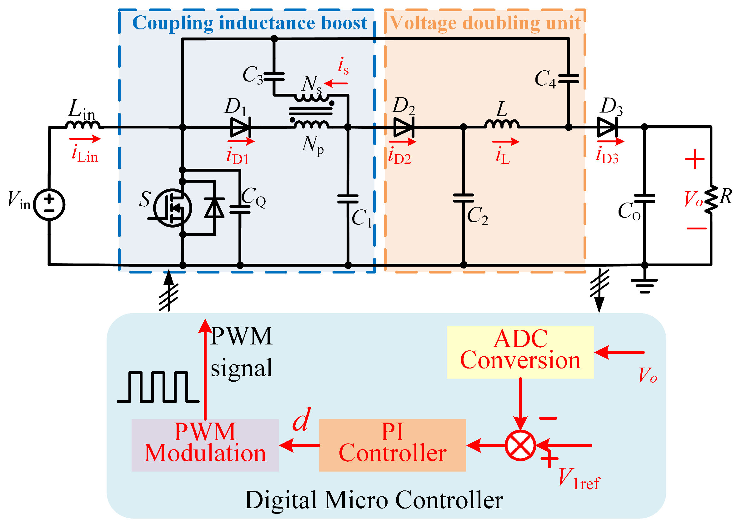
Figure 2.
The main waveform in a switching cycle.
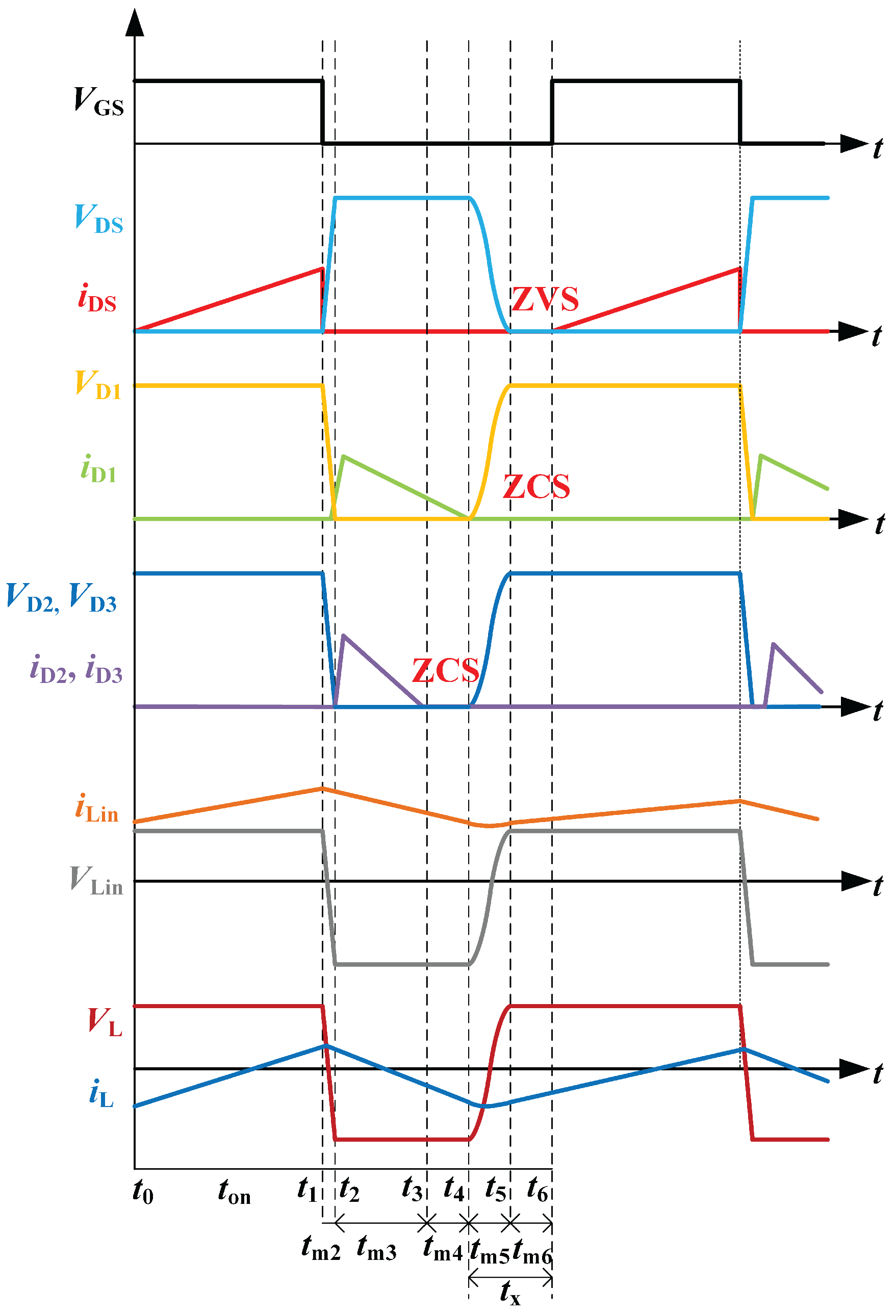
Figure 3.
This is the equivalent circuit for each mode of the circuit. The circuit has six states: (a) State 1 equivalent circuit. (b) State 2 equivalent circuit. (c) State 3 equivalent circuit. (d) State 4 equivalent circuit. (e) State 4 equivalent circuit. (f) State 6 equivalent circuit.
Figure 3.
This is the equivalent circuit for each mode of the circuit. The circuit has six states: (a) State 1 equivalent circuit. (b) State 2 equivalent circuit. (c) State 3 equivalent circuit. (d) State 4 equivalent circuit. (e) State 4 equivalent circuit. (f) State 6 equivalent circuit.
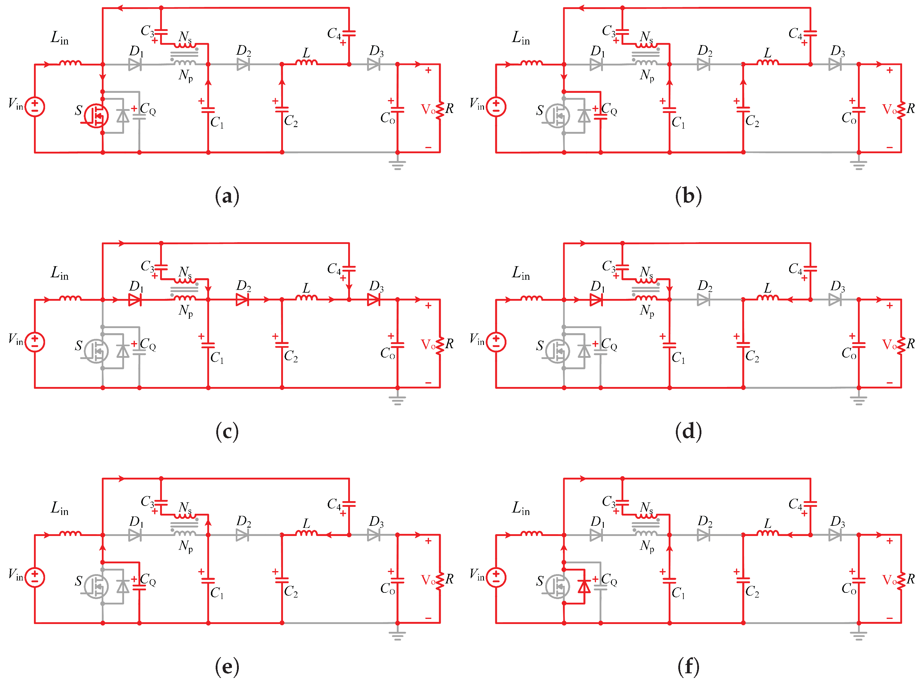
Figure 4.
Variation of voltage gain, duty cycle and time constant.
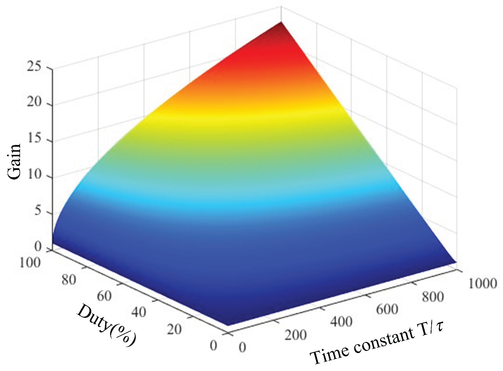
Figure 5.
Comparison of voltage gains among different converters.
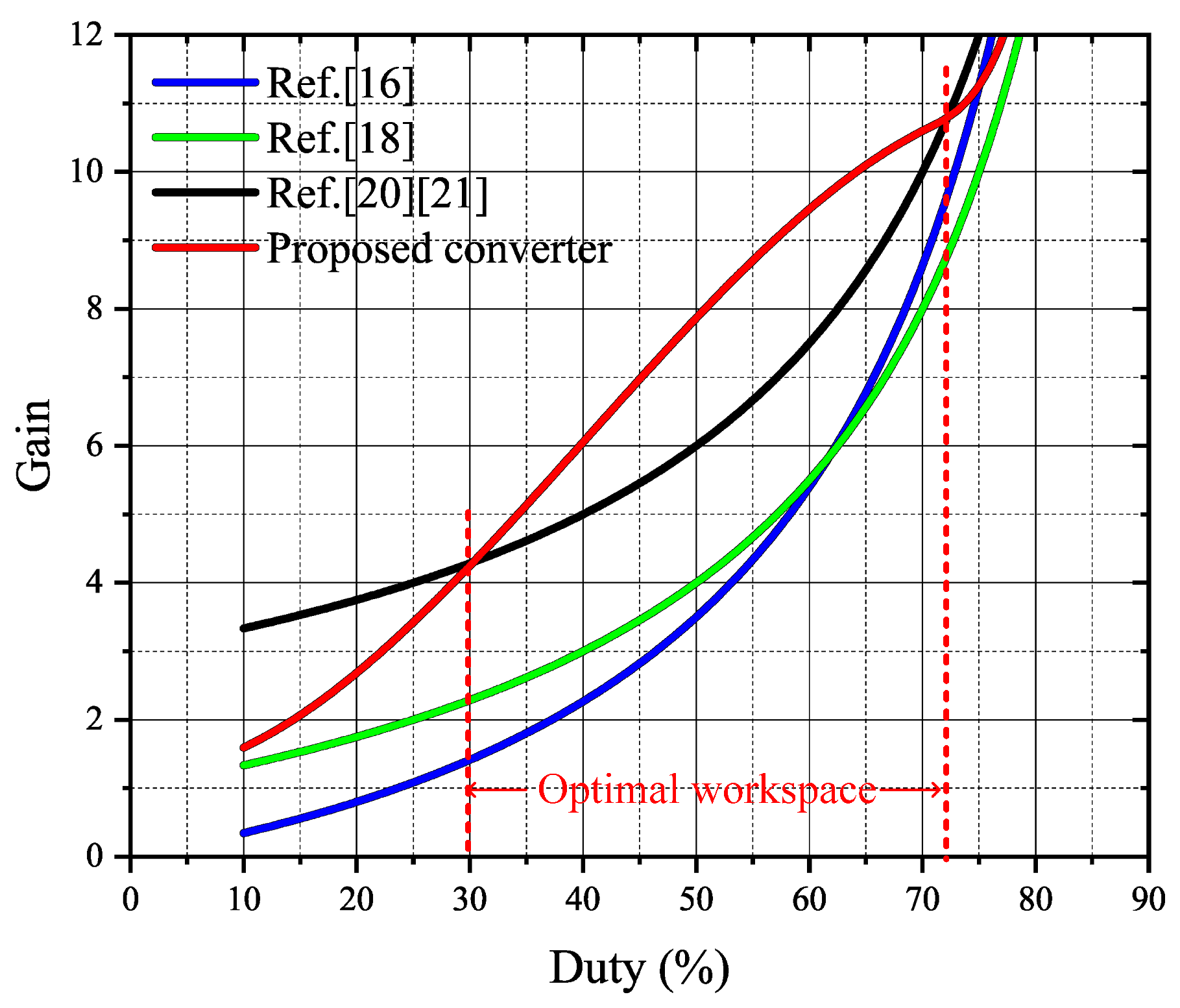
Figure 6.
Switching waveform during resonance.
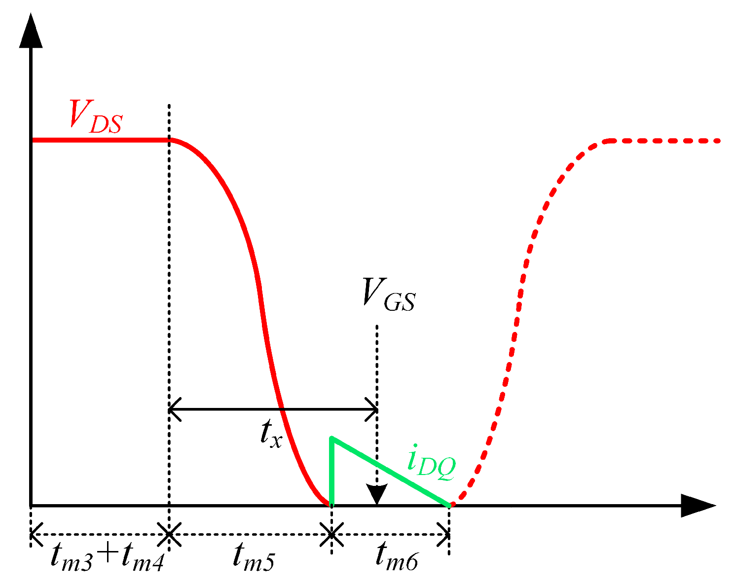
Figure 7.
ZVS simulation curve.
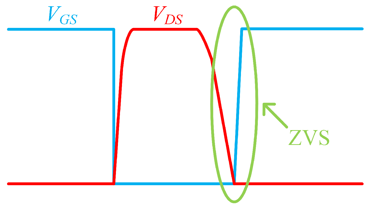
Figure 8.
Control block diagram for average output voltage.
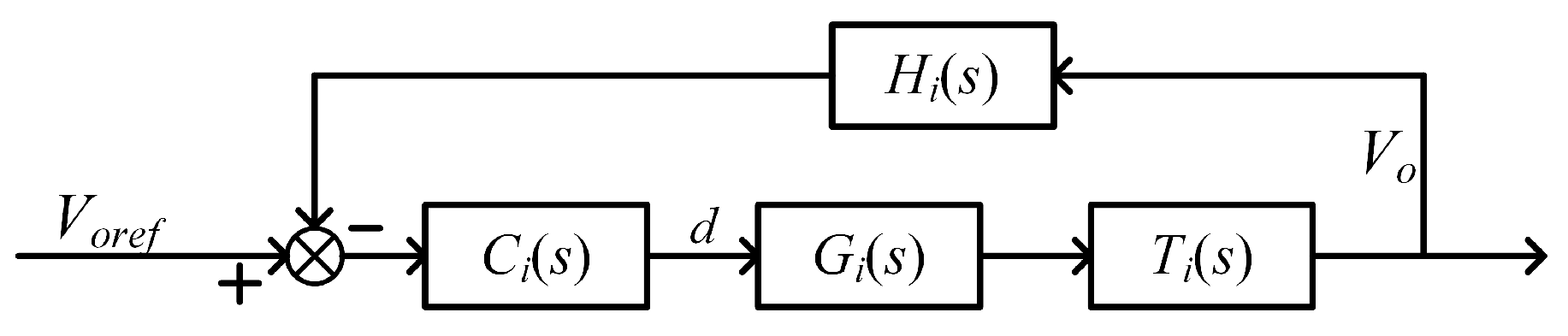
Figure 9.
Bode plot of open-loop transfer function before system compensation.
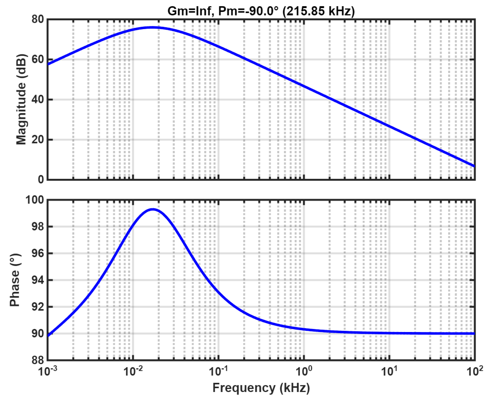
Figure 10.
Bode plot of open-loop transfer function after system compensation.
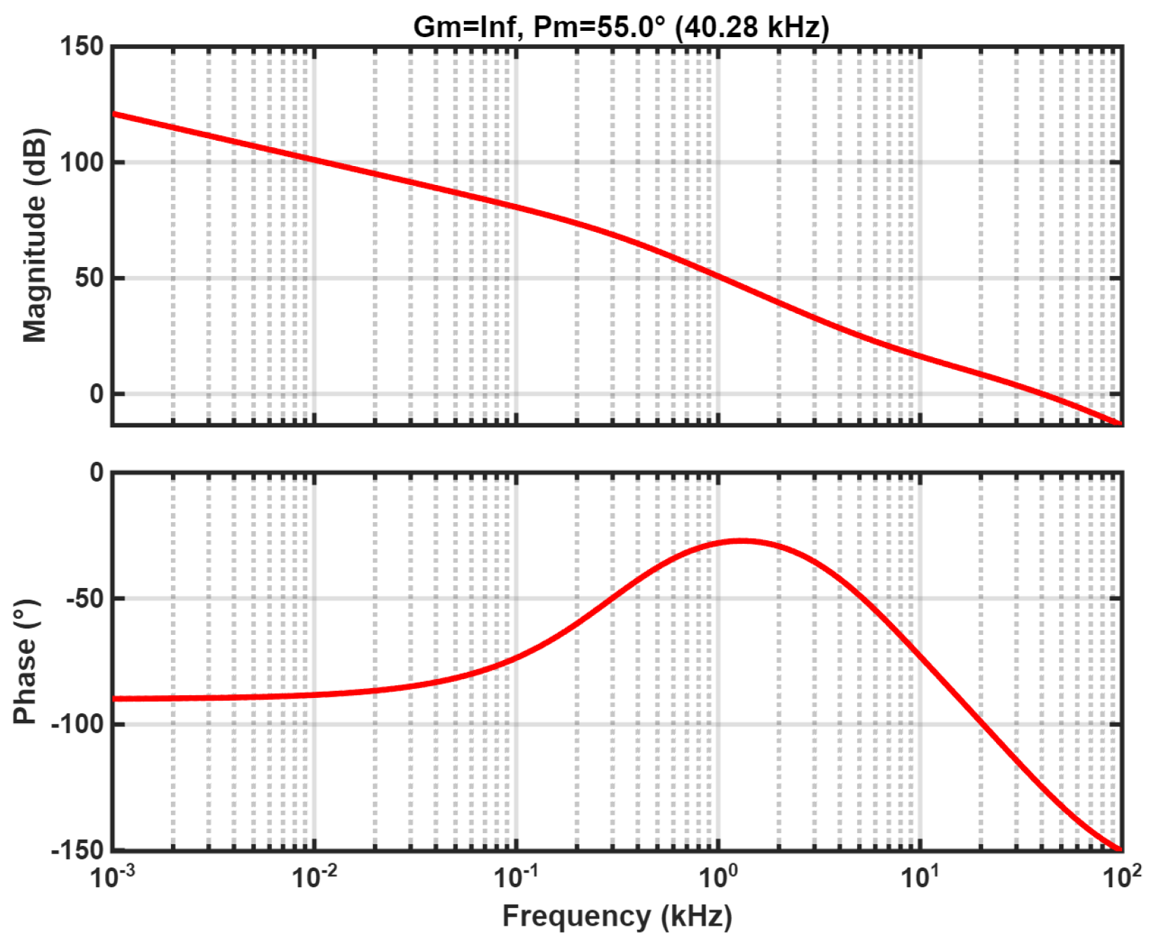
Figure 11.
Open-loop sweep curves of output voltage and voltage gain.
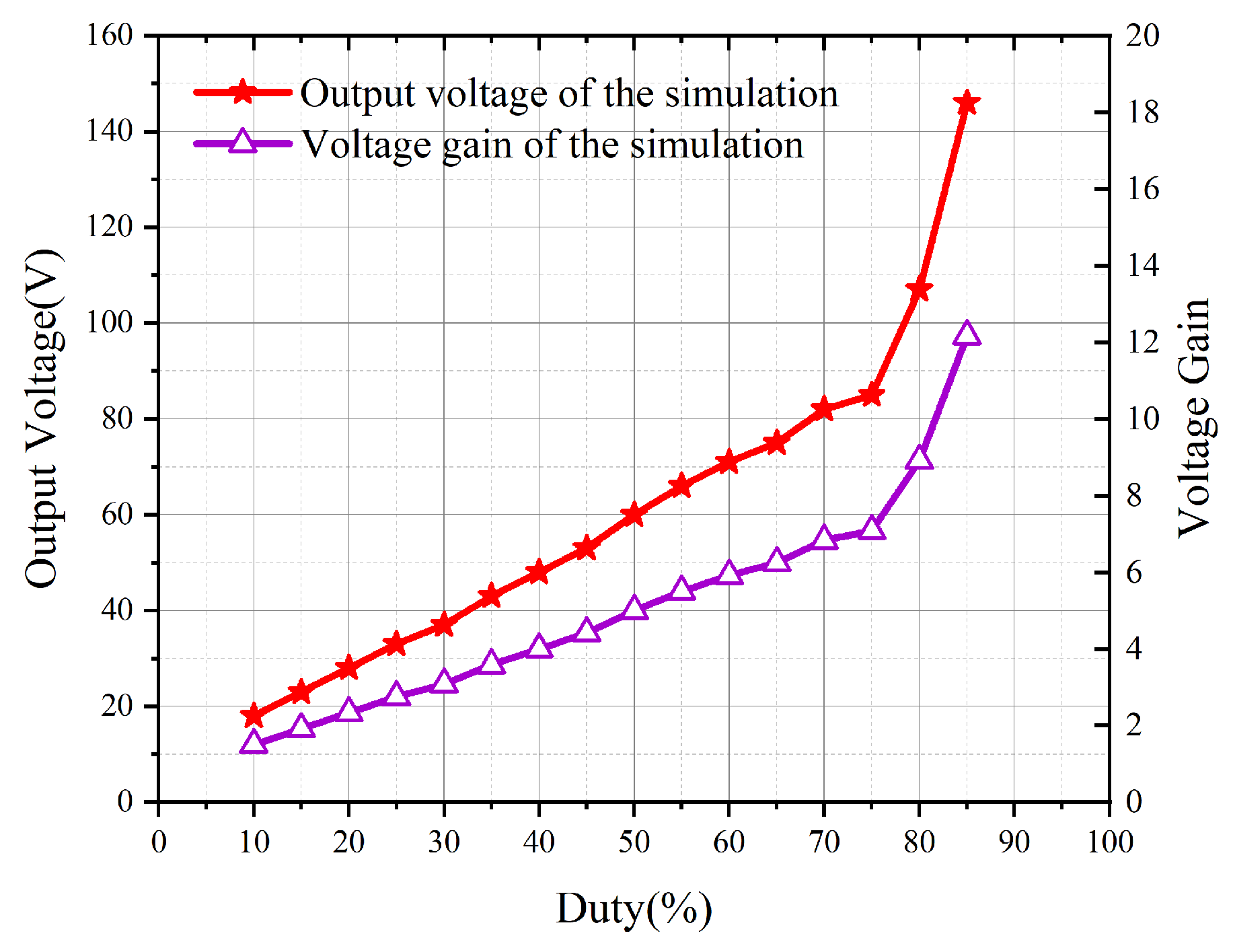
Figure 12.
Waveform of the input voltage with dynamic variations.
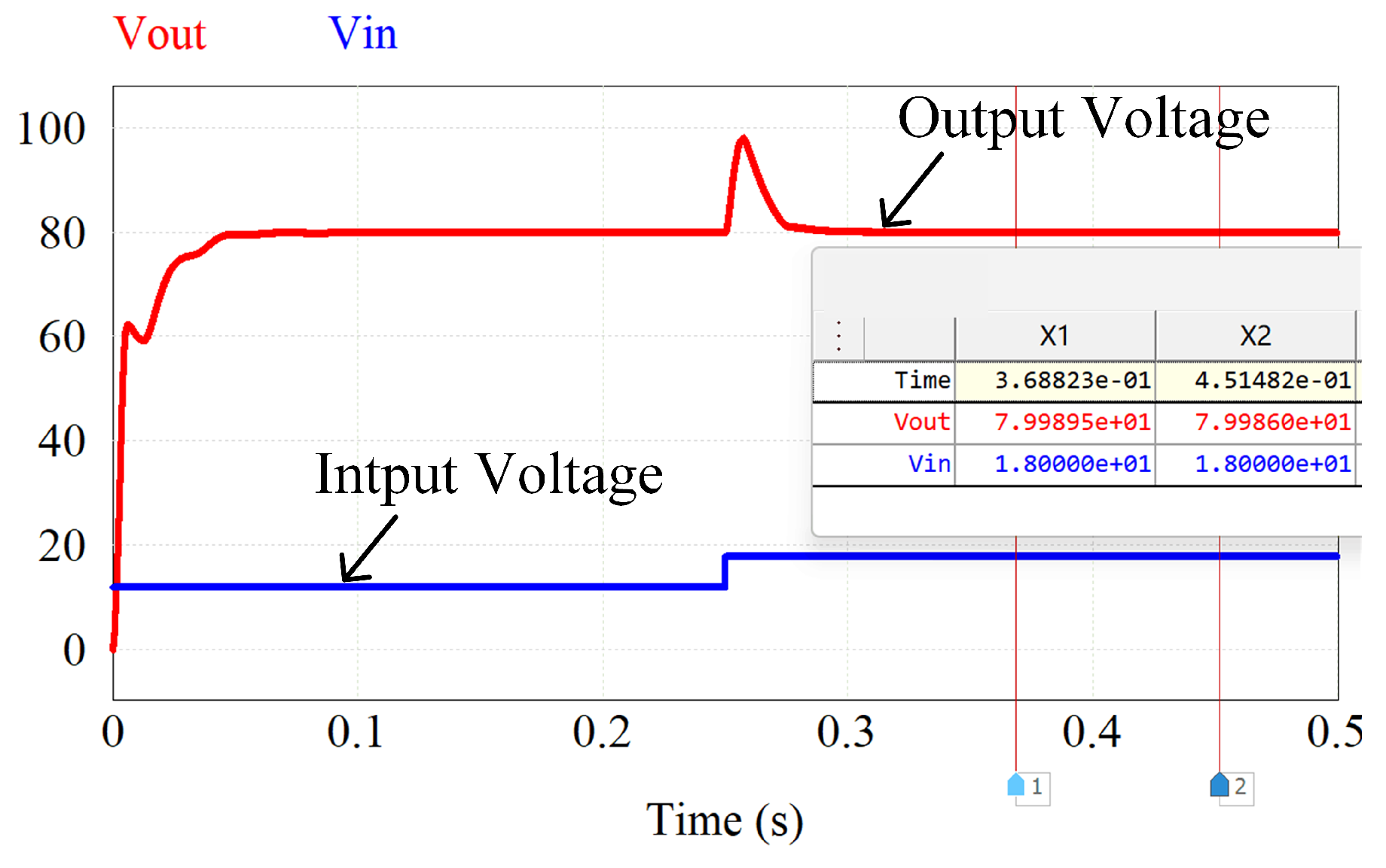
Figure 13.
Closed-loop simulation waveforms for sudden load changes.
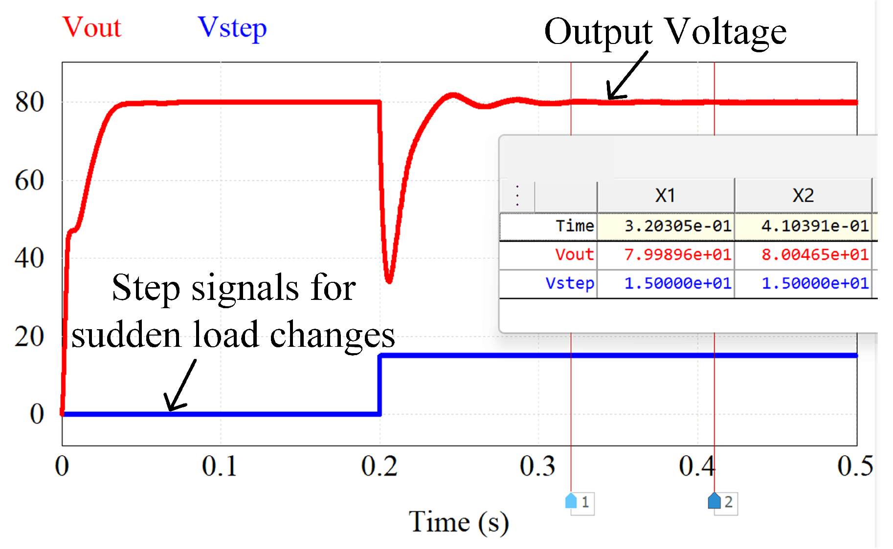
Figure 14.
Experimental platform.
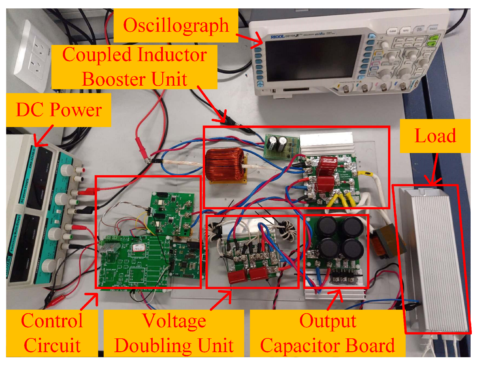
Figure 15.
Actual output voltage and gain open loop scan curve.
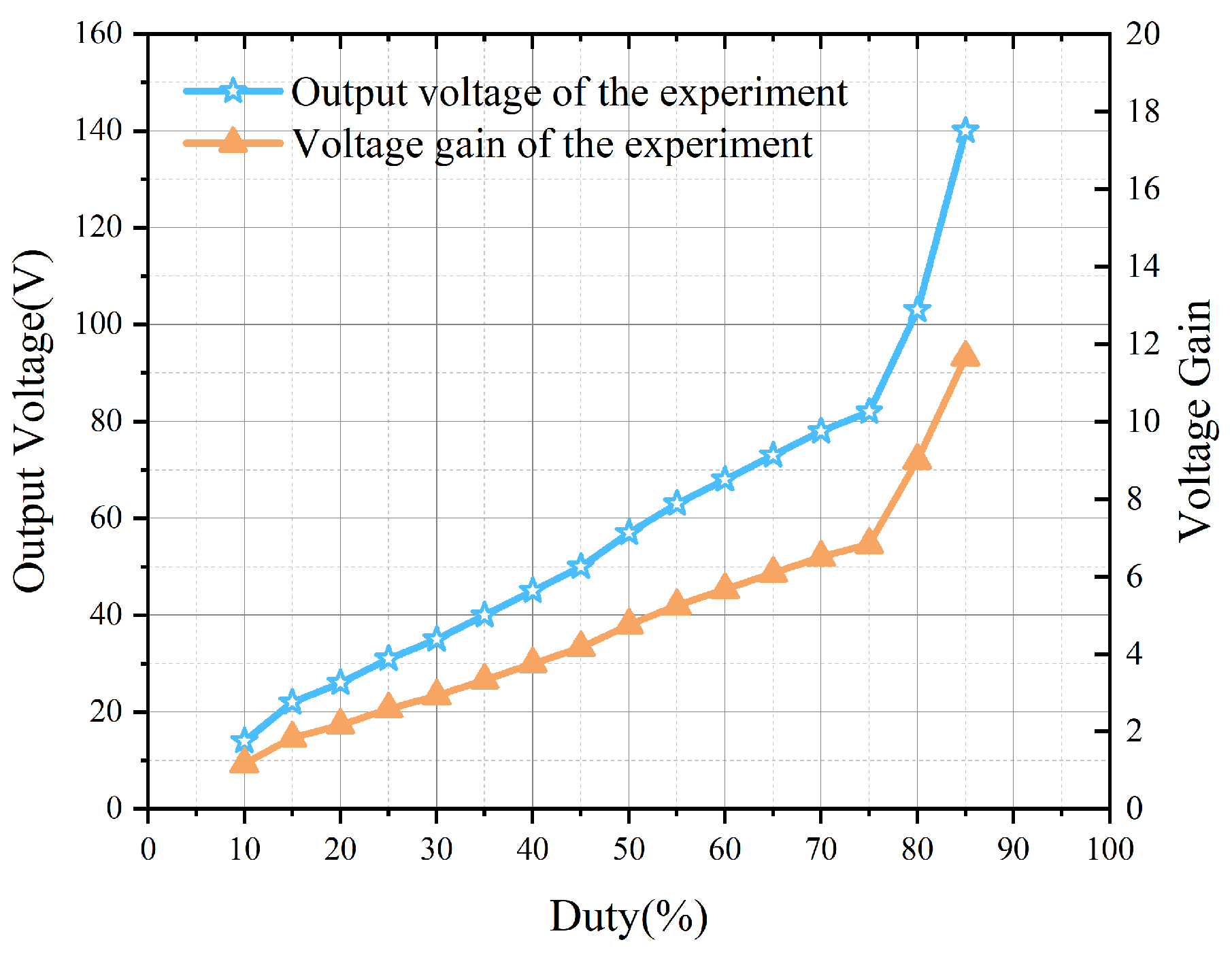
Figure 16.
Open-loop scan curve of converter efficiency.
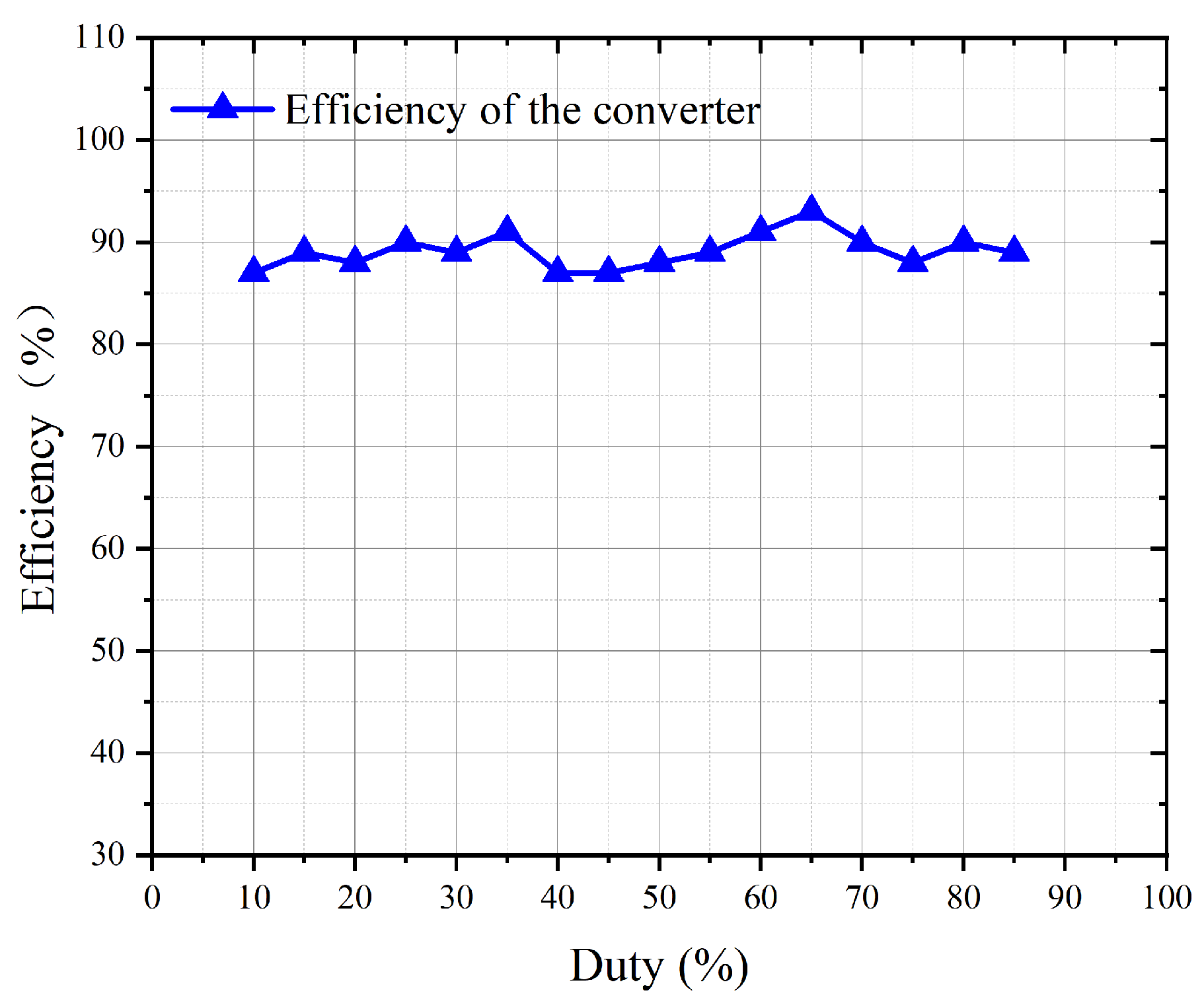
Figure 17.
Open-loop scanning of simulation and experimentation.
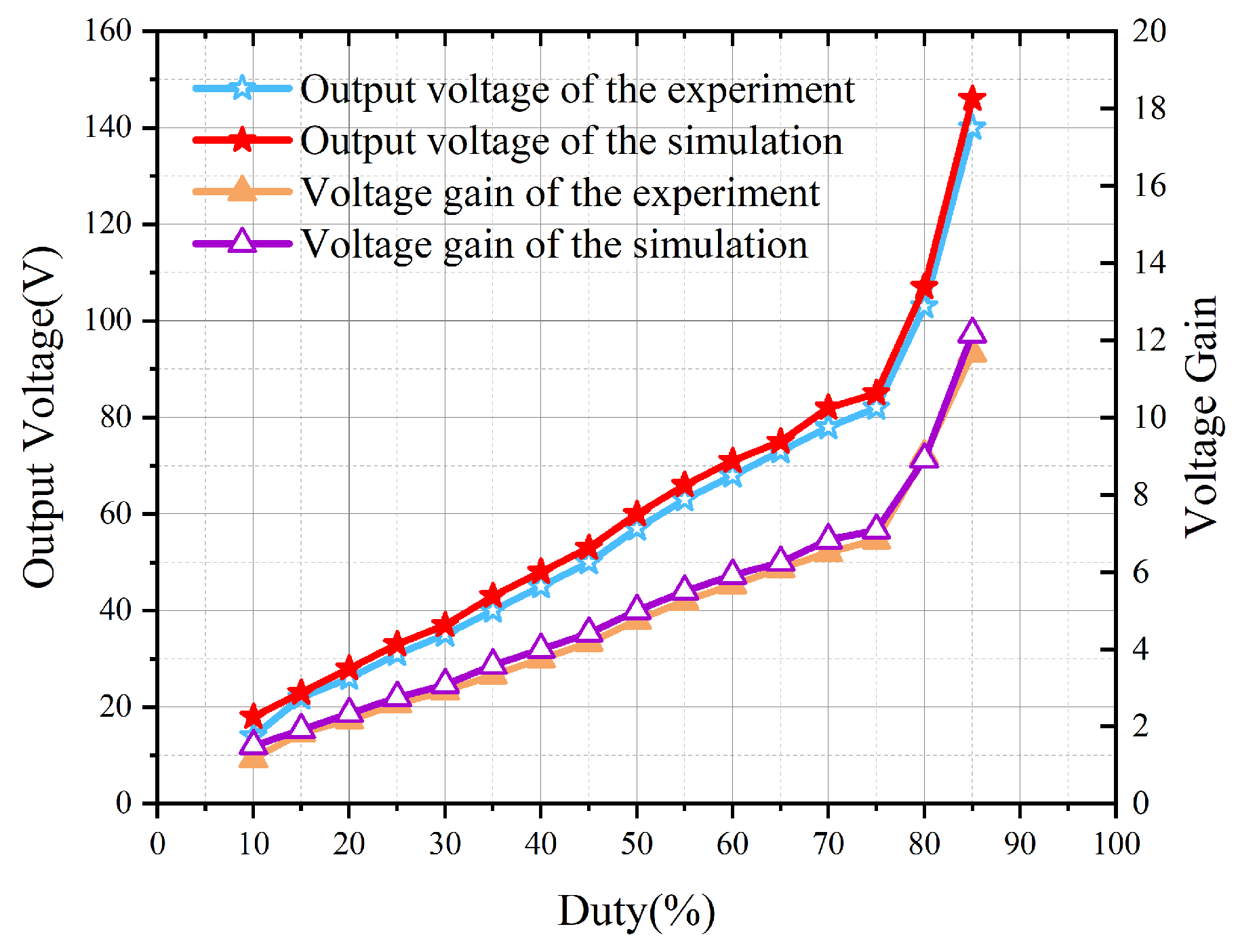
Figure 18.
This is the graph to verify the feasibility of the closed-loop system. The reference values of the output voltages are set to 70 V, 80 V and 100 V. The trigger waveform, steady state waveform and steady state duty cycle are measured. (a) =70V, D=0.50. (b) =80V, D=0.65. (c) =100V, D=0.80.
Figure 18.
This is the graph to verify the feasibility of the closed-loop system. The reference values of the output voltages are set to 70 V, 80 V and 100 V. The trigger waveform, steady state waveform and steady state duty cycle are measured. (a) =70V, D=0.50. (b) =80V, D=0.65. (c) =100V, D=0.80.
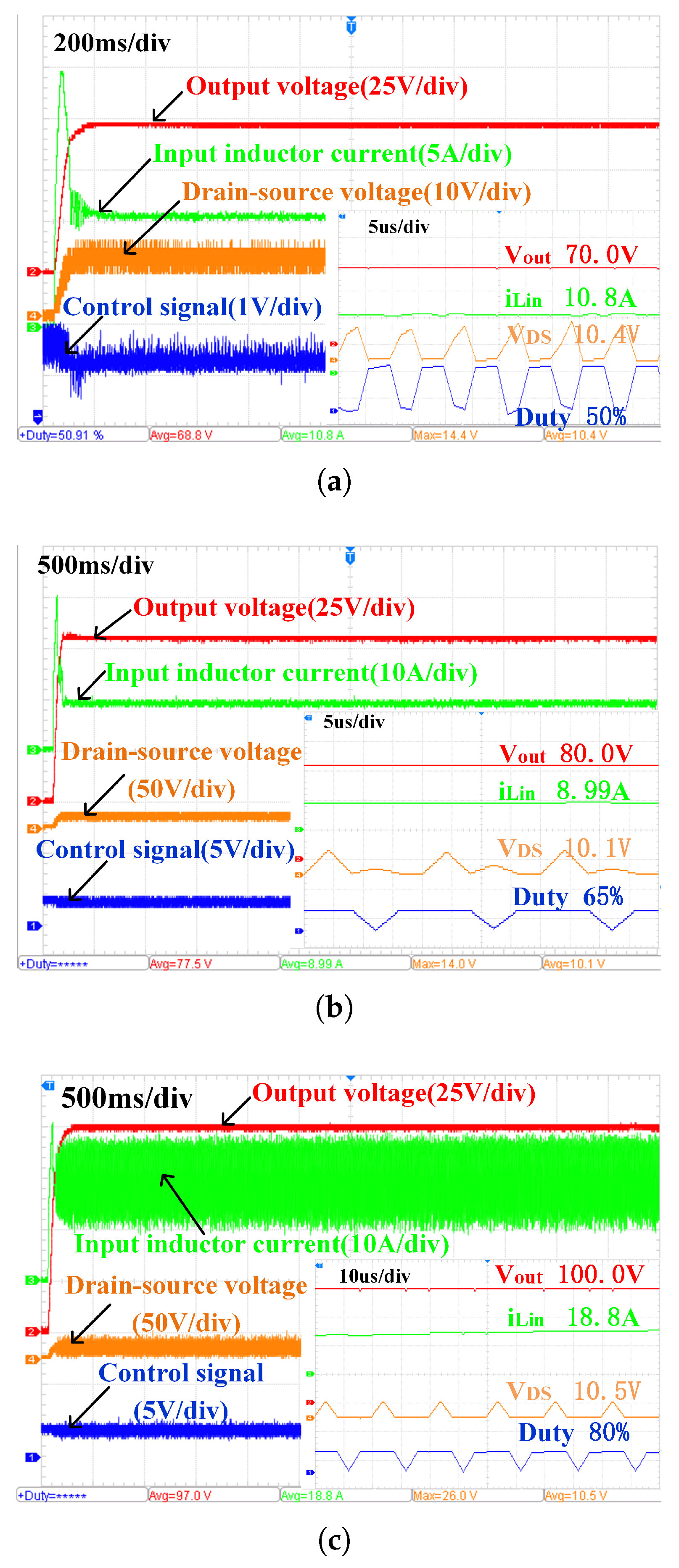
Figure 19.
Converter efficiency curve.
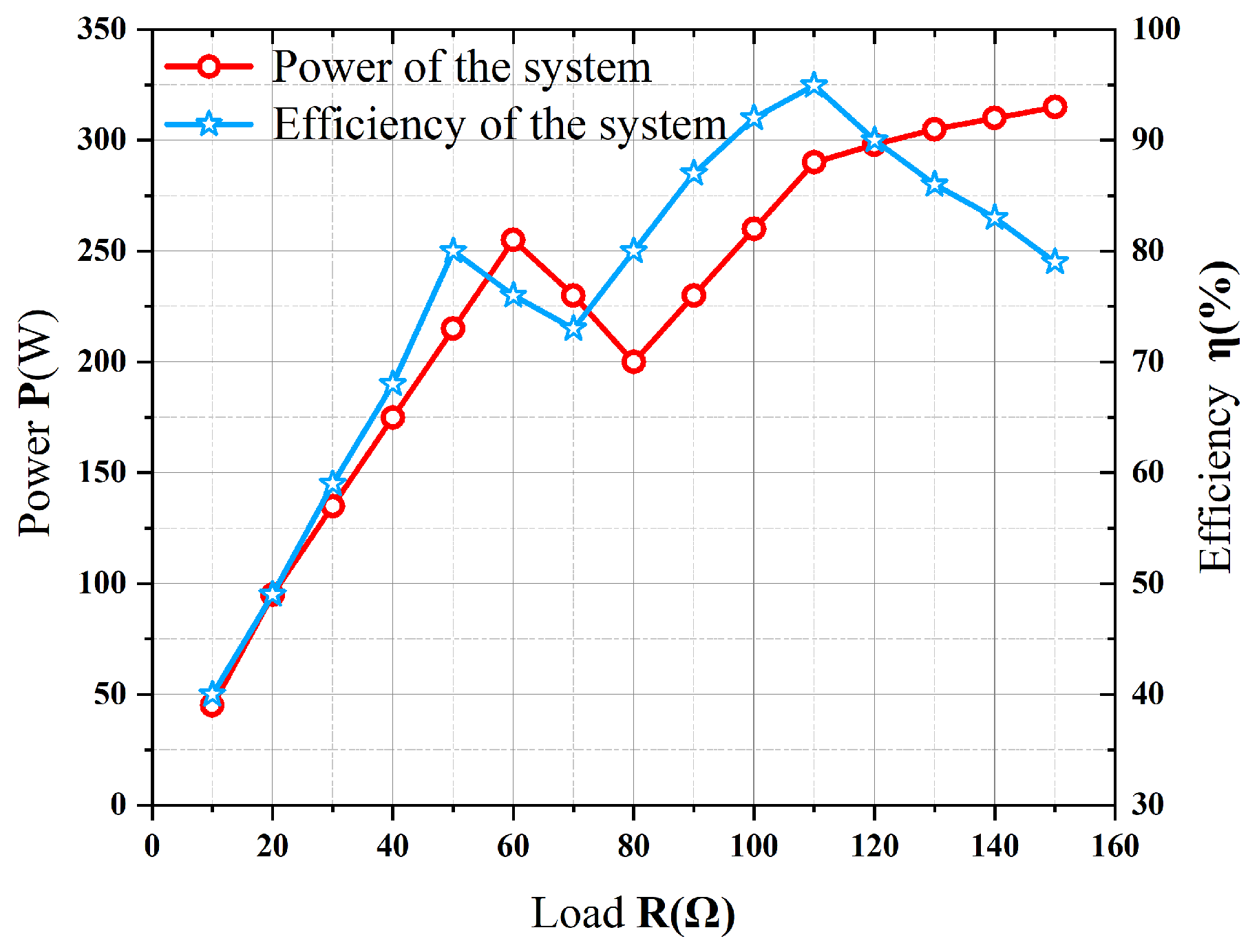

Table 1.
Performance Parameters Of Different Converters.
| Converter | Number of switches |
Number of diodes |
Switching voltage stress | Voltage gain |
|---|---|---|---|---|
| Ref. [16] | 1 | 4 | ||
| Ref. [18] | 2 | 8 | ||
| Ref. [20] | 2 | 4 | ||
| Ref. [21] | 1 | 3 | ||
| Proposed converter | 1 | 3 |
Table 2.
Main Circuit Parameters of Experimental Prototype.
| Mods | Model number |
|---|---|
| 100 kHz | |
| DPF30I300PA | |
| , | |
| , | |
| 1mH, | |
| n | |
| Load R |
Disclaimer/Publisher’s Note: The statements, opinions and data contained in all publications are solely those of the individual author(s) and contributor(s) and not of MDPI and/or the editor(s). MDPI and/or the editor(s) disclaim responsibility for any injury to people or property resulting from any ideas, methods, instructions or products referred to in the content. |
© 2025 by the authors. Licensee MDPI, Basel, Switzerland. This article is an open access article distributed under the terms and conditions of the Creative Commons Attribution (CC BY) license (http://creativecommons.org/licenses/by/4.0/).
Copyright: This open access article is published under a Creative Commons CC BY 4.0 license, which permit the free download, distribution, and reuse, provided that the author and preprint are cited in any reuse.


