
Submitted:
07 July 2025
Posted:
08 July 2025
You are already at the latest version
Abstract
If electronics manufacturers and users are to have confidence in the reliability of the solder joints on which they rely, it is essential to have an understanding of the solder joint failure mechanisms and the role of dynamic recrystallisation in failure. However, due to difficulties in real-time atomistic scale analysis during deformation, we still do not fully understand these mechanisms. Here, we report the development of an innovative in-situ method using high voltage transmission electron microscopy (HV-TEM) for observation of the microstructural response of a solder joint to room temperature tensile loading. This technique was used to observe events including dislocation formation, dynamic recrystallisation, grain boundary separation, and crack formation and propagation in a Sn-3wt.%Ag-0.5wt.%Cu (SAC305) alloy joint formed between copper substrates.
Keywords:
electronics packaging
; Pb-free solder
; in-situ deformation
; high-voltage transmission electron microscopy
1. Introduction
Tin (Sn)-based alloys that wet and react with copper (Cu) substrates to form solder joints remain an essential part of the electronics manufacturing practice. During the process of soldering to Cu substrates a multi-phase structure is formed that typically includes intermetallic compounds (IMCs) such as Cu6Sn5 and Cu3Sn. In service these joints are subjected to mechanical stresses that result from mismatches in the coefficients of thermal expansion (CTE) of the components and the substrates to which they are attached during the thermal cycles generated by the operation of the device and/or the environment to which the device is exposed [1,2,3,4,5,6,7,8,9,10]. The solder joint failure mechanism is complex and dependent on the stress, the rate at which it is applied, the temperature and the previous thermal history as well as the composition of the alloy and substrate [9,10]. Failure may occur between the substrate and the IMC layer, between the solder and the IMC layer, or in the bulk solder [11,12,13,14,15,16]. Numerous researchers have found a relationship between the recrystallisation of the β-Sn phase that occurs during thermal cycling and the path followed by the cracks that ultimately cause joint failure [10,17]. While this work has drawn attention to the role that strain-induced recrystallisation can play in solder joint failure mechanisms, it is based on examination of cross-sections of joints taken from the thermal cycling chamber at intervals during the expected time to failure. While representing a significant advance of our understand of the solder joint failure mechanism, these studies can tell only part of the story of solder joint failure in service. Despite advances in atomic scale in-situ analysis [18,19,20], the mechanisms of recrystallisation and crack propagation during solder joint deformation are not fully understood. As well as contributing to solder joint failure, it has been reported that recrystallisation can play a role in the processes that result in the growth of tin whiskers [21,22]. Tin whiskers are recognised cause of failure in critical circuitry and a better understanding of recrystallisation could therefore be a useful contributor to the formulation of whisker resistant solder alloys. An understanding of the recrystallisation mechanisms and the relationship to crack initiation and propagation in solder joints based on real time in-situ observation could provide a stronger basis for the formulation of solder alloys that can deliver more reliable interconnects on electronic circuitry.
This paper reports recent advances in the in-situ observation of dynamic recrystallisation and crack propagation in a Sn-3wt%Ag-0.5wt%Cu/Cu joint during room temperature tensile loading.
2. Materials and Methods
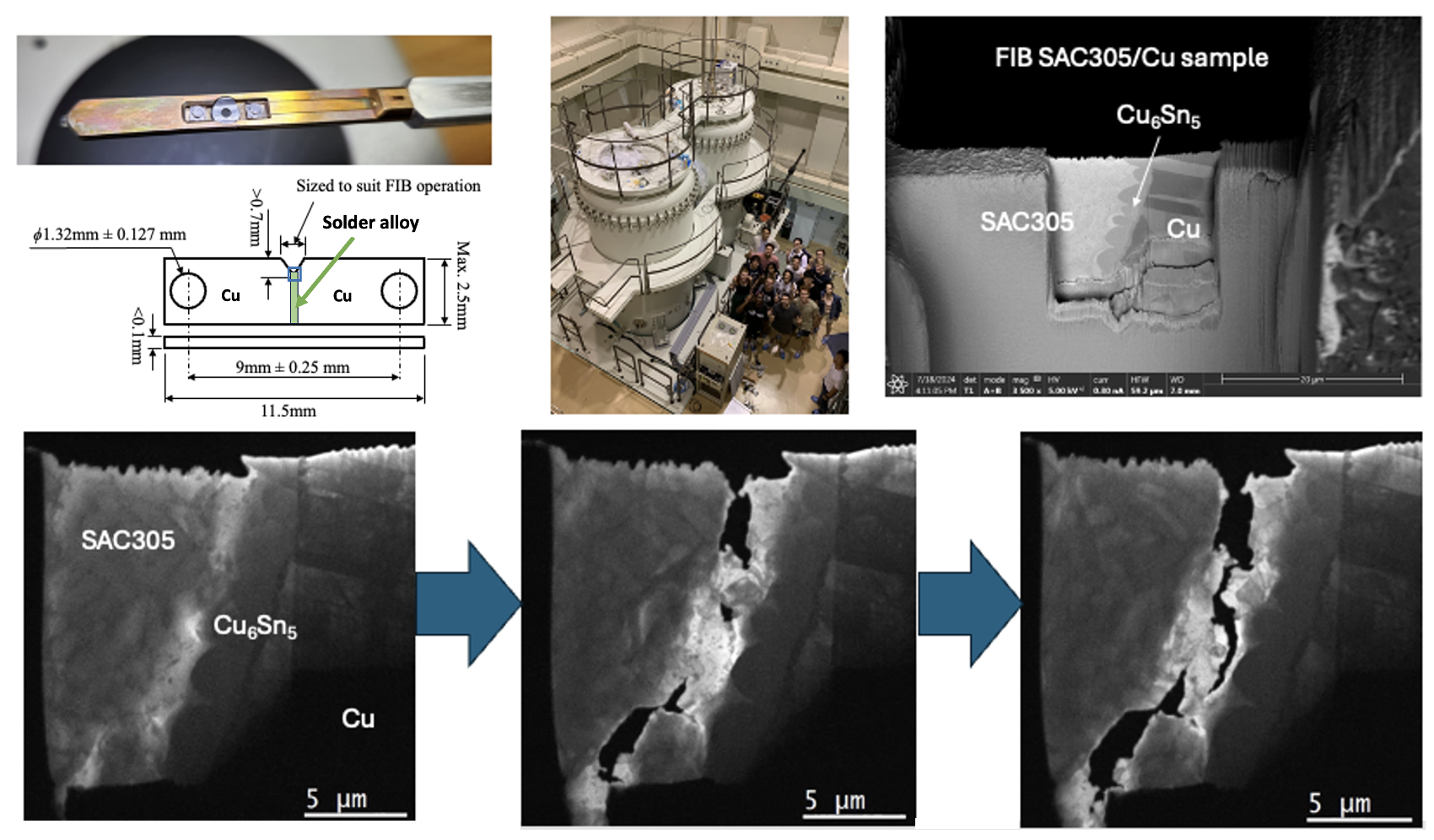
Two laser-cut notched Cu plates (thickness of <0.1mm) were hand-soldered using Sn-3wt.%Ag-0.5wt.%Cu (SAC305) solder (supplied by Nihon Superior Co. Ltd., Osaka, Japan) with a soldering iron set at 350°C, to fabricate a Cu/SAC305/Cu solder joint, as shown in Figure 1. An electron-transparent region, (approximately 0.5 μm in thickness) was prepared at the tip of the notch using a focused ion beam (FIB) milling process (FEI, Scios FIB - Dual Beam SEM). A platinum-rich precursor was deposited to form a protective layer.
The sample was prepared for TEM observation by placing on a holder (Gatan, Single Tilt Heating Straining Holder, Model 672) in a HV-TEM (JEOL, JEM-1300NEF) operated at an accelerating voltage of 1,250 kV with the Omega-type energy-filter. Tensile strain was applied at a crosshead speed of 1.0 μm/s. Due to the complex sample geometry, the loading is not purely tensile but the results nevertheless provide a new insight into the failure mechanism in solder joints and, in particular, the role recrystallisation in the deformed area plays in the ultimate failure. Video was recorded at a rate of 10 frames per second during tensile loading. The average strain rate of the sample was measured in the direction of crosshead travel from the recorded video (Video S1) as shown in Figure 2 and was approximately 0.0015s-1.
3. Results and Discussion
Energy-filtered TEM images of the observation area in the SAC305/Cu6Sn5/Cu3Sn/Cu sample before tensile loading shows the dendritic primary Sn within the SAC305 solder alloy microstructure (in Figure 3(a)) along with the layer of Cu6Sn5. At higher magnification (in supplemental Figure 3(b)), the eutectic Ag3Sn phase is visible in the interdendritic regions, along with a 2-3 μm thick, scalloped layer of Cu6Sn5 and a sub-micron thick Cu3Sn layer adjacent the Cu substrate. This distribution of phases is typical of the joint microstructure that results from the reaction between liquid SAC305 and the Cu substrate followed by solidification during soldering.
The entire experimental in-situ observations are provided as supplemental Video S1 (x30). Figure 4(a)-(f), Figure 5(a)-(c) and supplemental Video S2a (x4) shows in-situ TEM during tensile loading of the SAC305/Cu6Sn5/Cu, solder connection revealing deformation, dislocation accumulation and crack formation and propagation and the related formation of recrystallised grain boundaries. The observations were successful in identifying the moment of crack initiation in the SAC305 solder alloy, which occurred in the β-Sn adjacent to the Cu6Sn5 intermetallic, but not within Cu6Sn5 or Cu3Sn or the interface between the SAC305 solder and Cu6Sn5. This mode of failure is similar to that observed in SAC305 solder joints to ball grid array (BGA) packages during thermal cycling [6,7,8,9,10,15].
The crack path in the area of dislocation accumulation adjacent to the Cu6Sn5 intermetallics, followed the recrystallised grain boundaries, which were revealed by variations in contrast in the TEM images with the strain due to the dislocations and new grain boundary movement as well as bend contours movement, displayed dynamic behaviour during tensile loading. Due to the time resolution limit of 10 frames per second, it was difficult to record the moment of recrystallisation (see Figure 6), however, crack initiation and propagation along with dislocation accumulation were clearly observable (e.g., Figure 4 (c) - (f)).
During continued tensile loading, multiple dislocations could be seen in front of the tip of the advancing crack that migrate to nearby subgrain boundaries, growing recrystallised grains as well as nucleating new subgrains, in a process of discontinuous recrystallisation (DDRX) (in Figure 6), similar to refs. [5,23,24,25]. There are two main mechanisms in the process of recrystallisation [23,24,26], (i) discontinuous or classical dynamic recrystallisation (DDRX), occurring by nucleation and growth of new grains consuming rapidly the surrounding strain hardened matrix, and (ii) continuous dynamic recrystallisation (CDRX) involving the generation of new grain boundaries by the progressive misorientation of neighbouring subgrains by dislocation climb. Since we found new grains at the tip of the crack and a low density of dislocations after dynamic recrystallisation, the mechanism operating is expected to be (i) a DDRX mechanism, as evident in Figure 4(d) and (e), Figure 5, Figure 6 and supplemental Video S2a. This mechanism corresponds well with the report by B. Zhou et. al.[25] that shows the recrystallisation process at a solder/substrate interface during thermal cycling.
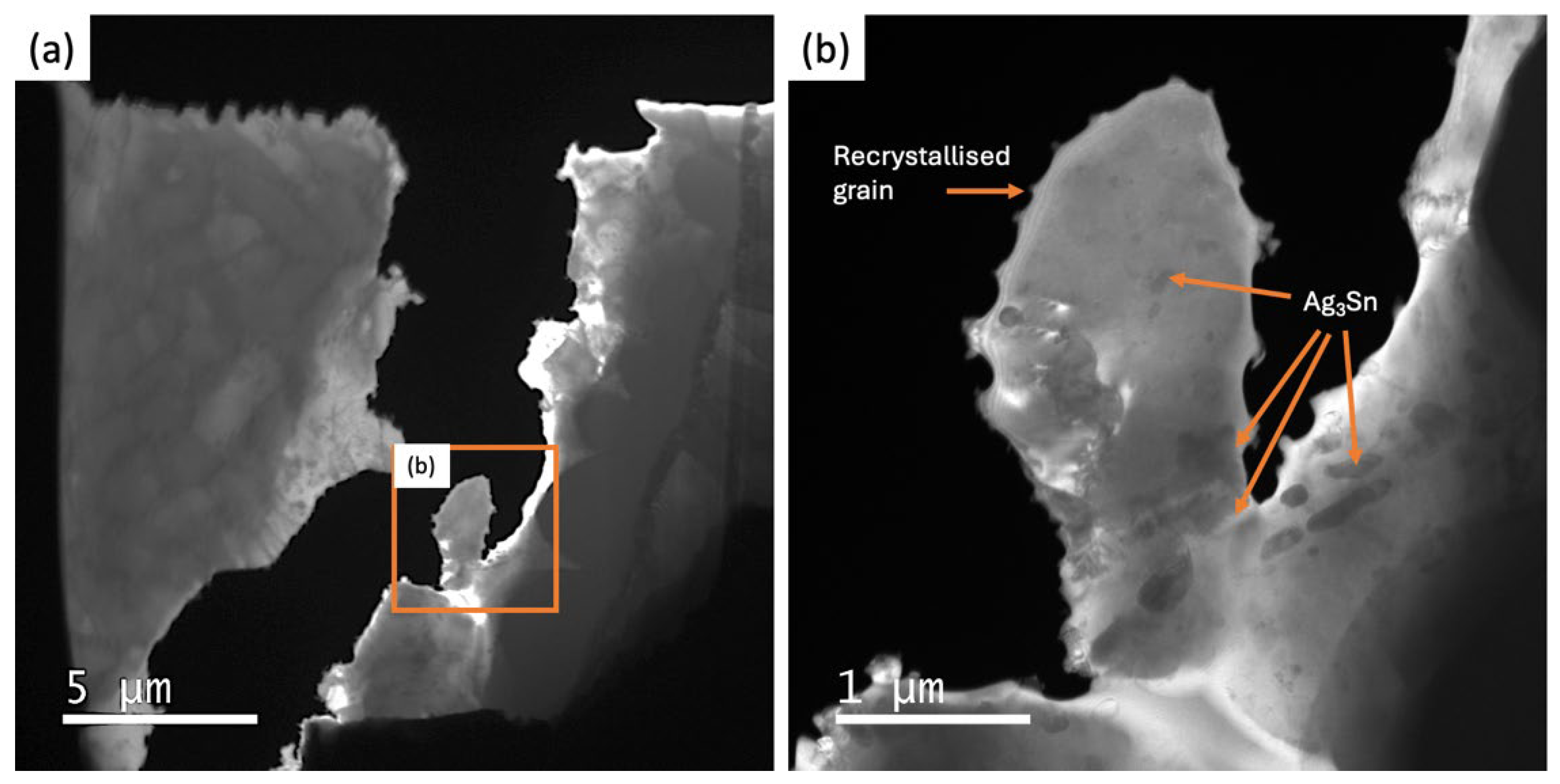
Figure 7(a)-(f), 8(a)-(d) and supplemental Video S2b (x4) show higher magnification imaging after recrystallisation and continued crack propagation. It can be seen that the recrystallised grain boundary sliding and subsequent recrystallised grain separation together represent the crack propagation event. Bieler et. al. [5] reported cracks form at random recrystallised boundaries, which then spread through recrystallised regions. Our observations provide clear visual evidence of this cracking process. There is some Ag3Sn remaining in the recrystallised grains but most of the Ag3Sn particles are present along the grain boundaries or in the non-recrystallised regions, as can be seen in supplemental Figure 9. This result is consistent with previous work on thermally cycled BGAs that reported that coarsened Ag3Sn particles are often located at recrystallised grain boundaries whereas the interior of recrystallised grains are, in many places, particle free zones [10]. This suggests that the design of crack-resistant BGAs should further consider the effect of IMC particles on both recrystallisation and crack growth processes, including the interactions between recrystallisation and accelerated particle coarsening.
4. Conclusions
In conclusion, we successfully fabricated a mechanical test specimen with a microstructure representative of a typical SAC305 solder joint that was locally thinned for in-situ TEM observation using HV-TEM. The observations during deformation showed the moment of crack initiation and the relationship between dynamic recrystallisation and crack propagation, both of which were observed in-situ, during tensile loading at room temperature. The processes of dislocation accumulation and nucleation of new grains through discontinuous recrystallisation, and the importance of recrystallised grain boundary sliding and subsequent recrystallised grain separation during the crack propagation process were revealed. In the future this technique will be used to examine recrystallisation occurring in both static and dynamic loading over a range of temperatures in a variety of solder alloys.
Supplementary Materials
The following supporting information can be downloaded at the website of this paper posted on Preprints.org. Video S1. In-situ TEM video for whole tensile loading process.; Video S2a. In-situ TEM video for dislocation accumulation at crack tip and nucleation of recrystallised grains.; Video S2b. In-situ TEM video for grain boundary sliding and crack propagations.
Author Contributions
Conceptualisation, K.N., X.T., S.M., K.S. and K.Y.; methodology, J.Z., F.S., G.Z., K.N. and H.M.; validation, K.N., X.T., S.M. and C.G.; formal analysis, H.M. and K.N..; investigation, K.N. and H.M.; resources, K.N., X.T., and S.M.; writing—original draft preparation, K.N.; writing—review and editing, X.T., K.S., C.G, S.M., and K.N.; visualisation, K.N.; supervision, K.N.; project administration, K.N.; funding acquisition, K.N., X.T., and S.M. All authors have read and agreed to the published version of the manuscript.
Funding
This work is funded by the University of Queensland-Kyushu University (UQ-KU) Oceania project, the Advanced Research Infrastructure for Materials and Nanotechnology in Japan (ARIM) of the Ministry of Education, Culture, Sports, Science and Technology (MEXT) [JPMXP1224KU0032], Nihon Superior – the University of Queensland (UQ) collaborative grants [2021002341, 2024003478] and an ARC Discovery project [DP200101949].
Institutional Review Board Statement
Not applicable
Informed Consent Statement
Not applicable
Data Availability Statement
Not applicable
Acknowledgments
The authors acknowledge Mr Xiaozhou Ye (UQ) for strain rate measurement, the facilities and the scientific and technical assistance, of the Australian Microscopy & Microanalysis Research Facility at the Centre for Microscopy and Microanalysis, The University of Queensland, in particular for the access to the FIB SCIOS system for TEM sample preparation.
Conflicts of Interest
The authors declare no conflict of interest.
References
- Tu, P. L.; Chan, Y. C.; Lai, J. K. L. Effect of intermetallic compounds on the thermal fatigue of surface mount solder joints. IEEE Transactions on Components, Packaging, and Manufacturing Technology: Part B 1997, 20(1), 87–93. [Google Scholar] [CrossRef]
- Bieler, T. R.; Jiang, H.; Lehman, L. P.; Kirkpatrick, T.; Cotts, E. J. In Influence of Sn grain size and orientation on the thermomechanical response and reliability of Pb-free solder joints, 56th Electronic Components and Technology Conference 2006, 30 May-2 June 2006, 2006; p 6 pp.
- Davis, J. A.; Bozack, M. J.; Evans, J. L. Effect of (Au, Ni)Sn $_{4}$ Evolution on Sn-37Pb/ENIG Solder Joint Reliability Under Isothermal and Temperature-Cycled Conditions. IEEE Transactions on Components and Packaging Technologies 2007, 30(1), 32–41. [Google Scholar]
- Nousiainen, O.; Kangasvieri, T.; Rautioaho, R.; Vähäkangas, J. Thermal fatigue endurance of Sn3Ag0.5Cu0.5In0.05Ni and Sn2.5Ag0.8Cu0.5Sb solders in composite solder joints of LTCC/PWB assemblies. Soldering & Surface Mount Technology 2011, 23(1), 30–39. [Google Scholar] [CrossRef]
- Bieler, T. R.; Zhou, B.; Blair, L.; Zamiri, A.; Darbandi, P.; Pourboghrat, F.; Lee, T.-K.; Liu, K.-C. , The Role of Elastic and Plastic Anisotropy of Snin Recrystallization and Damage Evolution DuringThermal Cycling in SAC305 Solder Joints. J. Electron. Mater. 2012, 41(2), 283–301. [Google Scholar]
- Arfaei, B.; Mahin-Shirazi, S.; Joshi, S.; Anselm, M.; Borgesen, P.; Cotts, E.; Wilcox, J.; Coyle, R. In Reliability and failure mechanism of solder joints in thermal cycling tests, 2013 IEEE 63rd Electronic Components and Technology Conference, 28-31 May 2013, 2013; pp 976-985.
- Tegehall, P.-E.; Wetter, G. Impact of laminate cracks under solder pads on the fatigue lives of ball grid array solder joints. Microelectronics Reliability 2015, 55(11), 2354–2370. [Google Scholar] [CrossRef]
- Ben Romdhane, E.; Roumanille, P.; Guédon-Gracia, A.; Pin, S.; Nguyen, P.; Frémont, H. From early microstructural evolution to intergranular crack propagation in SAC solders under thermomechanical fatigue. Microelectronics Reliability 2021, 126, 114288. [Google Scholar] [CrossRef]
- Bender, E.; Bernstein, J. B.; Boning, D. S., Modern Trends in Microelectronics Packaging Reliability Testing. In Micromachines, 2024; Vol. 15. [CrossRef]
- Xian, J. W.; Xu, Y. L.; Stoyanov, S.; Coyle, R. J.; Dunne, F. P. E.; Gourlay, C. M. The role of microstructure in the thermal fatigue of solder joints. Nature Communications 2024, 15(1), 4258. [Google Scholar] [CrossRef]
- Darveaux, R.; Reichman, C.; Islam, N. In Interface failure in lead free solder joints, 56th Electronic Components and Technology Conference 2006, 30 May-2 June 2006, 2006; p 12 pp.
- Liu, D.-S.; Kuo, C.-Y.; Hsu, C.-L.; Shen, G.-S.; Chen, Y.-R.; Lo, K.-C. Failure mode analysis of lead-free solder joints under high speed impact testing. Materials Science and Engineering: A 2008, 494(1), 196–202. [Google Scholar] [CrossRef]
- Jing, J.; Gao, F.; Johnson, J.; Liang, F. Z.; Williams, R. L.; Qu, J. Brittle Versus Ductile Failure of a Lead-Free Single Solder Joint Specimen Under Intermediate Strain Rate. IEEE Transactions on Components, Packaging and Manufacturing Technology 2011, 1(9), 1456–1464. [Google Scholar] [CrossRef]
- Tsukamoto, H.; Nishimura, T.; Suenaga, S.; McDonald, S. D.; Sweatman, K. W.; Nogita, K. The influence of solder composition on the impact strength of lead-free solder ball grid array joints. Microelectronics Reliability 2011, 51(3), 657–667. [Google Scholar] [CrossRef]
- Coyle, R. J.; Sweatman, K.; Arfaei, B. Thermal Fatigue Evaluation of Pb-Free Solder Joints: Results, Lessons Learned, and Future Trends. JOM 2015, 67(10), 2394–2415. [Google Scholar]
- Min, K. E.; Jang, J. W.; Kang, S.; Kim, C.; Yi, S. Identification of Solder Joint Failure Modes Using Machine Learning. IEEE Transactions on Components, Packaging and Manufacturing Technology 2023, 13(12), 2032–2039. [Google Scholar] [CrossRef]
- Yin, L.; Wentlent, L.; Yang, L.; Arfaei, B.; Oasaimeh, A.; Borgesen, P. Recrystallization and Precipitate Coarsening in Pb-Free Solder Joints During Thermomechanical Fatigue. J. Electron. Mater. 2012, 41(2), 241–252. [Google Scholar] [CrossRef]
- Zhou, J.; Yao, T.; Cao, D.; Lian, J.; Lu, F. In-situ TEM study of radiation-induced amorphization and recrystallization of hydroxyapatite. J. Nucl. Mater. 2018, 512, 307–313. [Google Scholar] [CrossRef]
- Li, Z.; Zhang, L. In-situ TEM investigation of dislocation healing and recrystallization in nanoscratched silicon at elevated temperatures up to 800 °C. Journal of Materials Research and Technology 2024, 31, 1939–1944. [Google Scholar] [CrossRef]
- Hu, X. J.; Sun, W.; Liao, J. L.; Zhang, Y. H.; Wang, B.; Shuai, S. S.; Liu, C.; Zeng, G. The influences of microstructural length scale on the tensile properties and deformation mechanisms of Sn-3.0Ag-0.5Cu solder alloys. Materials Science and Engineering: A 2024, 916, 147300. [Google Scholar] [CrossRef]
- Chang, J.; Kang, S. K.; Lee, J.-H.; Kim, K.-S.; Lee, H. M. Recrystallization as a Growth Mechanism for Whiskers on Plastically Deformed Sn Films. J. Electron. Mater. 2015, 44(10), 3486–3499. [Google Scholar] [CrossRef]
- Kuwano, N.; Binti Lias, M.; Nordin, N. A.; Soejima, Y.; bin Nayan, A. R. Preliminary Study on Deformation and Recrystallization Behavior of Pure Tin for Mitigation of Whisker Growth. Solid State Phenomena 2018, 273, 107–111. [Google Scholar] [CrossRef]
- Montheillet, F.; Lépinoux, J.; Weygand, D.; Rauch, E. , Dynamic and Static Recrystallization. Adv. Eng. Mater. 2001, 3(8), 587–589. [Google Scholar]
- Huang, K.; Logé, R. E. A review of dynamic recrystallization phenomena in metallic materials. Materials & Design 2016, 111, 548–574. [Google Scholar] [CrossRef]
- Zhou, B.; Bieler, T. R.; Lee, T.-k.; Liu, W. Characterization of Recrystallization and Microstructure Evolution in Lead-Free Solder Joints Using EBSD and 3D-XRD. J. Electron. Mater. 2013, 42(2), 319–331. [Google Scholar] [CrossRef]
- Sunada, T.; Otsuka, M.; Yamagata, H.; Fujiwara, M. Dynamic Recrystallization of Pure Tin. J. Japan Inst. Metals 1999, 63(4), 467–473. [Google Scholar] [CrossRef]
Figure 1.
Sample geometry for in-situ tensile loading experiment in high-voltage TEM. An electron-transparent region is prepared at the tip of the notch using FIB.
Figure 1.
Sample geometry for in-situ tensile loading experiment in high-voltage TEM. An electron-transparent region is prepared at the tip of the notch using FIB.
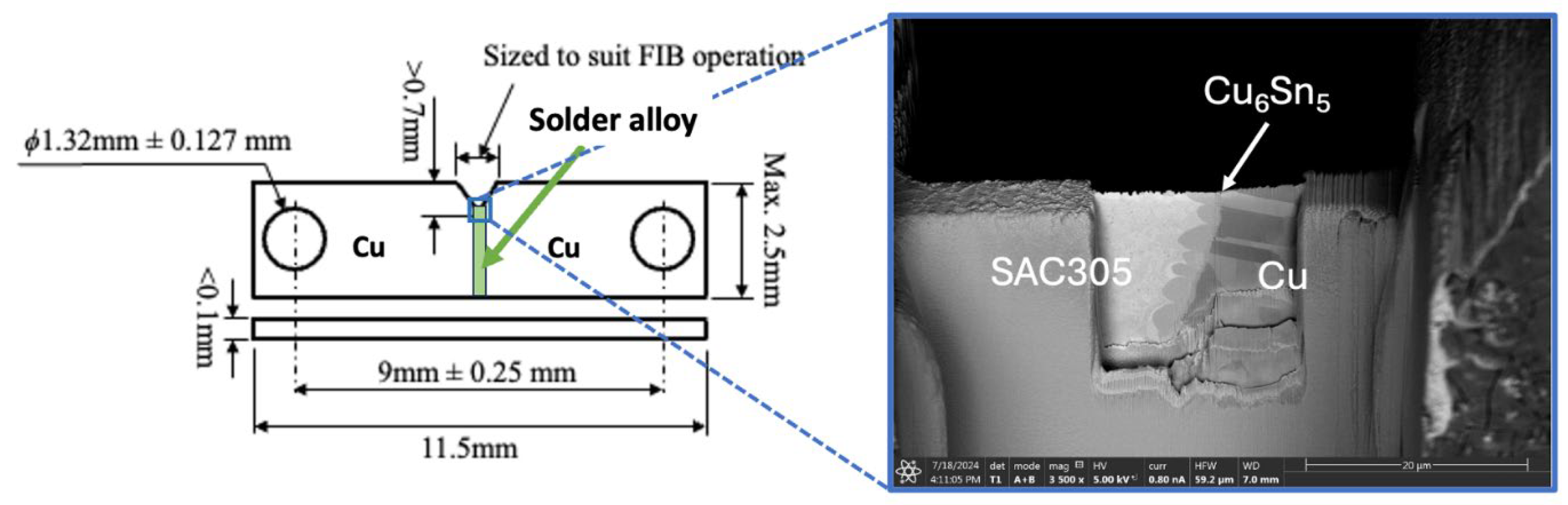
Figure 2.
(a) Strain (%) and (b) average strain rate (%s-1), measured from Video S1.
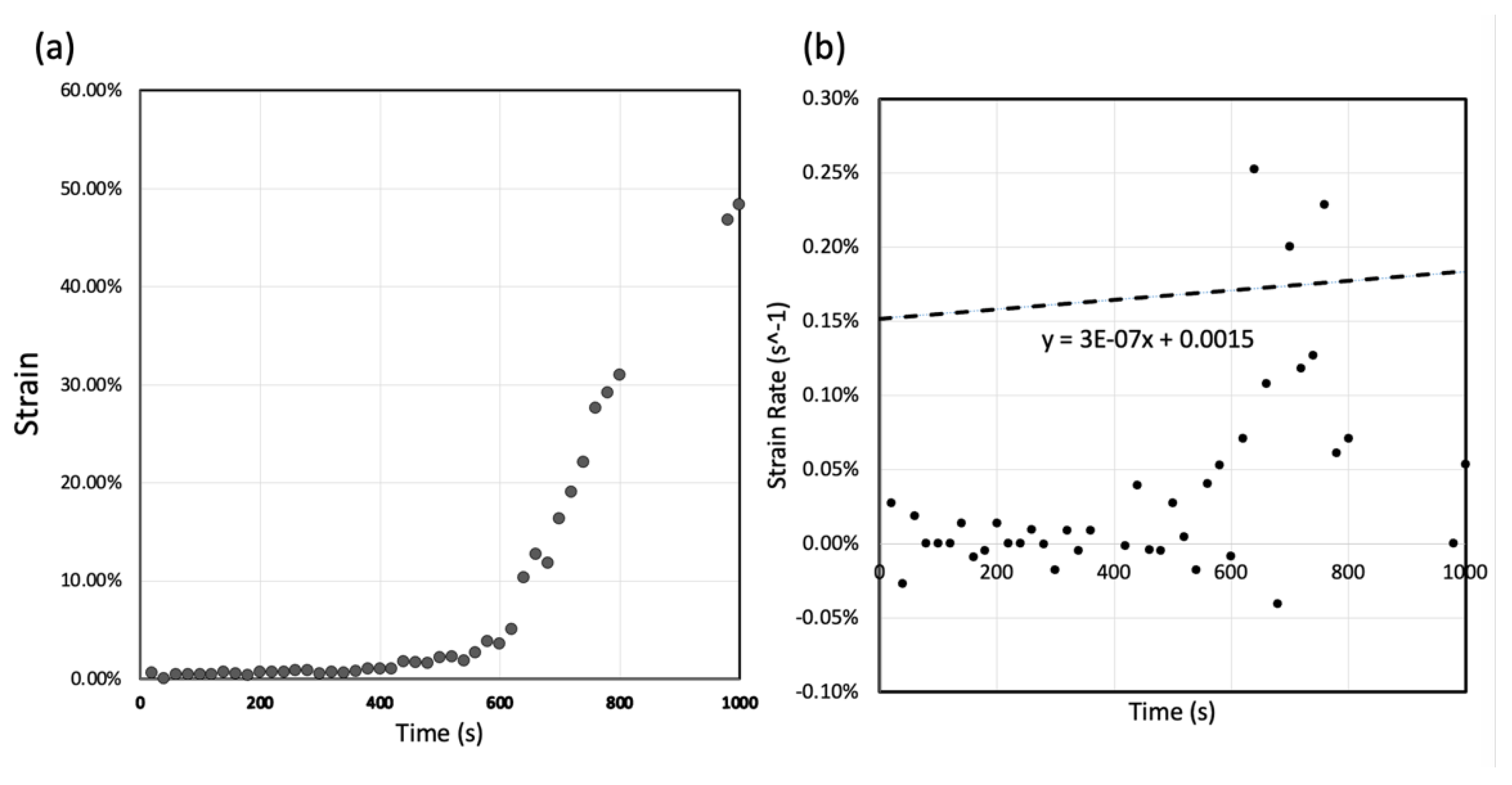
Figure 3.
Energy-filtered TEM images of the solder joint observation area before tensile loading, (a) low magnification and (b) high magnification. Tensile loading is in the horizontal direction at a crosshead speed of 1.0 μm/s.
Figure 3.
Energy-filtered TEM images of the solder joint observation area before tensile loading, (a) low magnification and (b) high magnification. Tensile loading is in the horizontal direction at a crosshead speed of 1.0 μm/s.
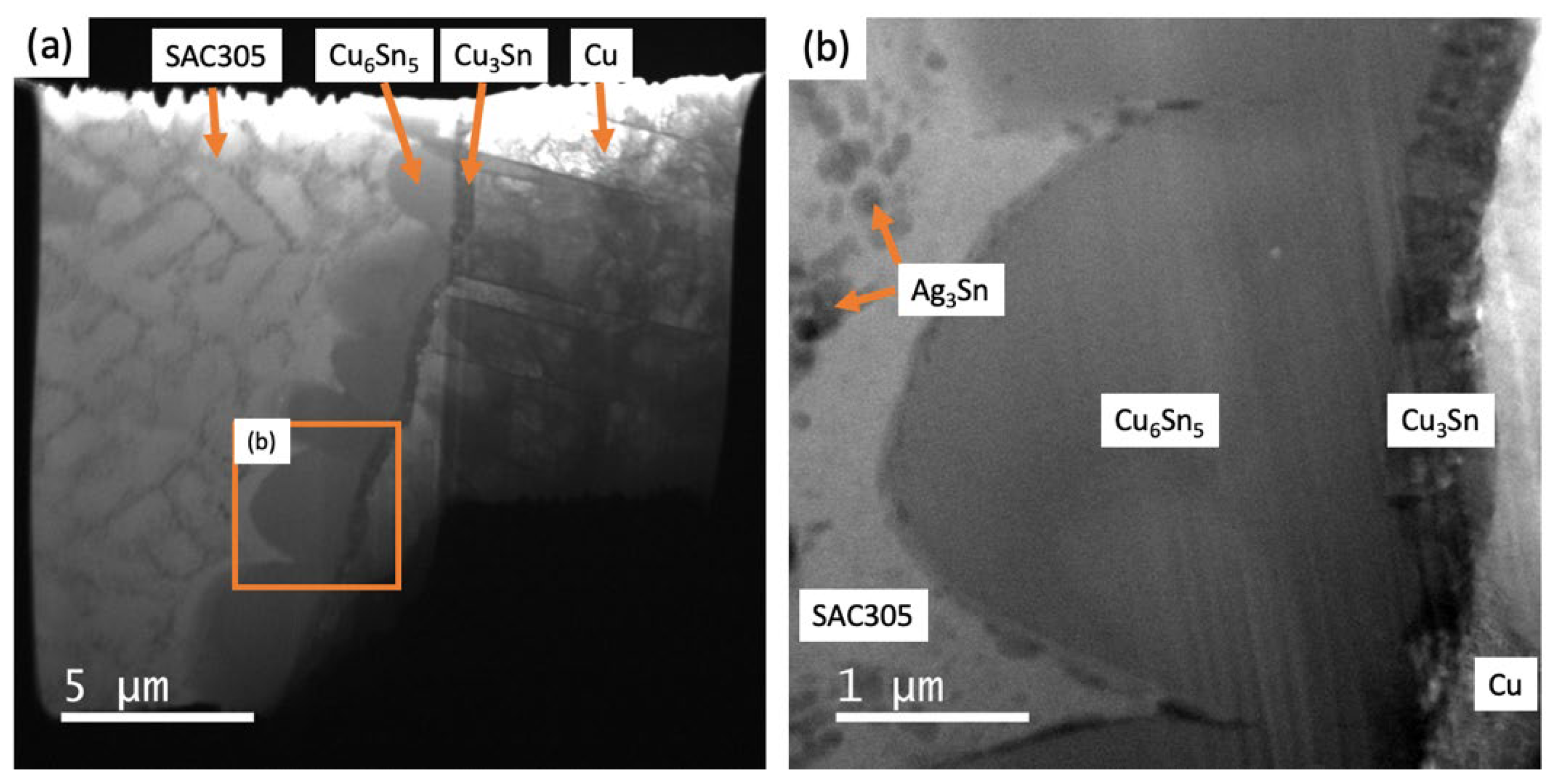
Figure 4.
Still images from supplemental Video S2a. In-situ TEM observations of the solder joint with a tensile loading at a crosshead speed of 1.0 μm/s. (a) and (b) Sample thickness (indicated by brightness) is reducing in the area of the SAC305 solder adjacent to the Cu6Sn5, (c) crack initiation occurs in several regions, (d) dislocation accumulation at the crack propagation front, (e) and (f) crack propagation in the boundaries between recrystallised grains.
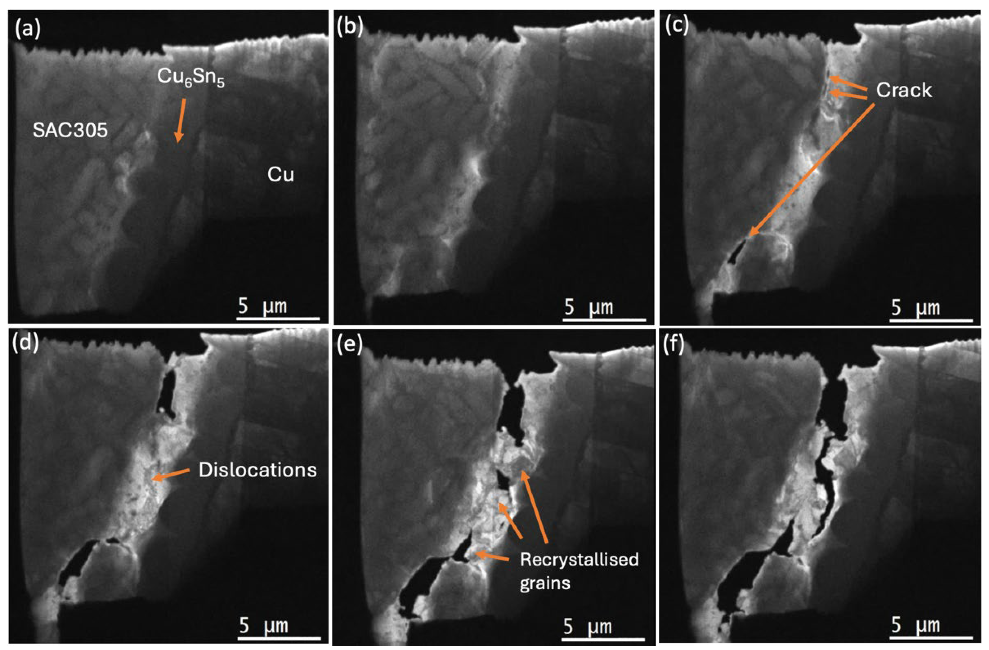
Figure 5.
Still images from supplemental Video S2a. Crack propagation process, (a) Dislocation accumulation, (b) Crack formation and nucleation of new grains, (c) Crack propagations along new grain boundaries.
Figure 5.
Still images from supplemental Video S2a. Crack propagation process, (a) Dislocation accumulation, (b) Crack formation and nucleation of new grains, (c) Crack propagations along new grain boundaries.
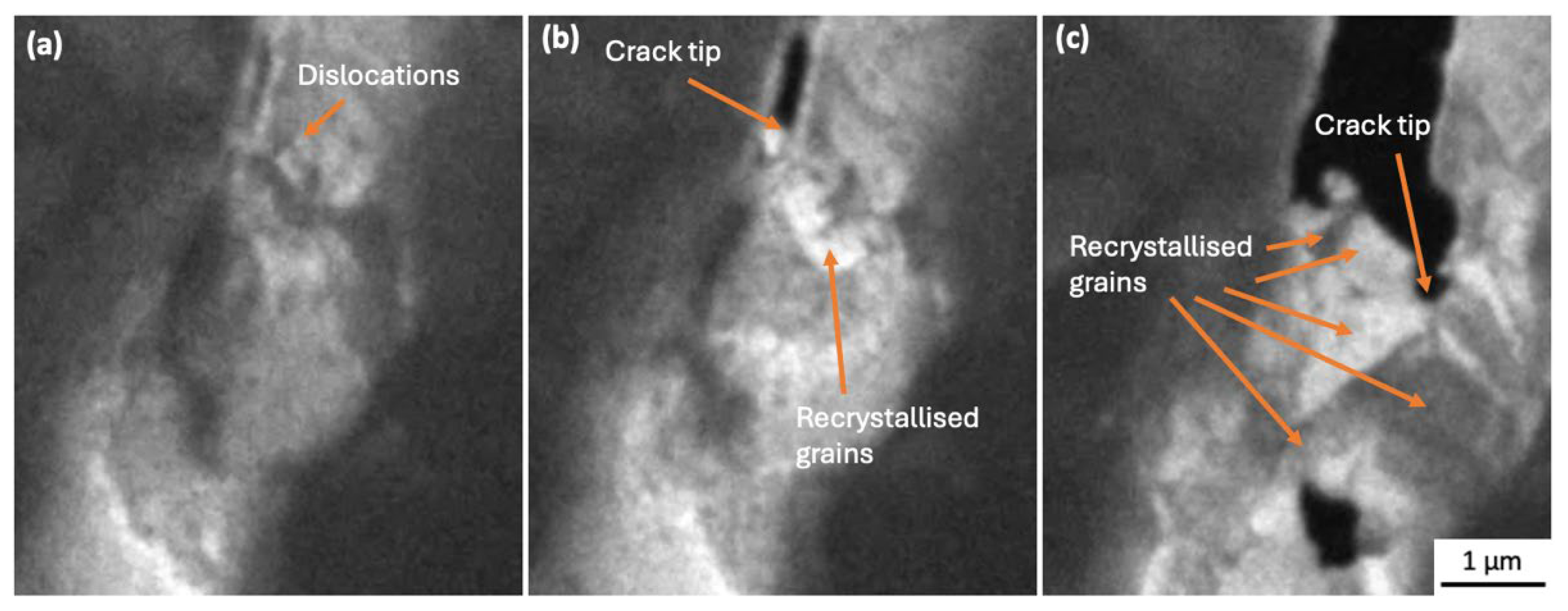
Figure 6.
Still images from supplemental Video S2b. Recrystallised grains nucleate at dislocation pile-up at crack tip, (a) Nucleation of recrystallised grains, (b)-(d) Growth of recrystallised grains.
Figure 6.
Still images from supplemental Video S2b. Recrystallised grains nucleate at dislocation pile-up at crack tip, (a) Nucleation of recrystallised grains, (b)-(d) Growth of recrystallised grains.
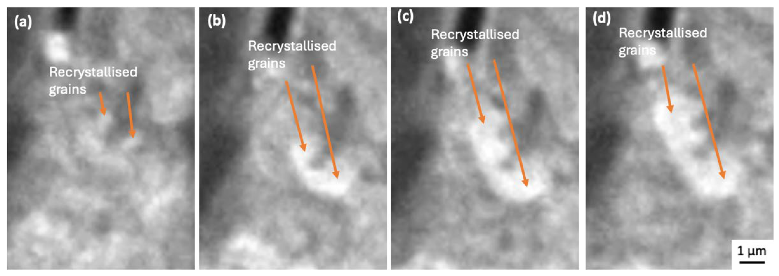
Figure 7.
Still images from supplemental Video S2b. In-situ energy-filtered TEM images of the solder joint with tensile loading at a crosshead speed of 1.0 μm/s, after crack formation. The process of crack propagation along with sliding at the boundaries of recrystallised grains is apparent.
Figure 7.
Still images from supplemental Video S2b. In-situ energy-filtered TEM images of the solder joint with tensile loading at a crosshead speed of 1.0 μm/s, after crack formation. The process of crack propagation along with sliding at the boundaries of recrystallised grains is apparent.
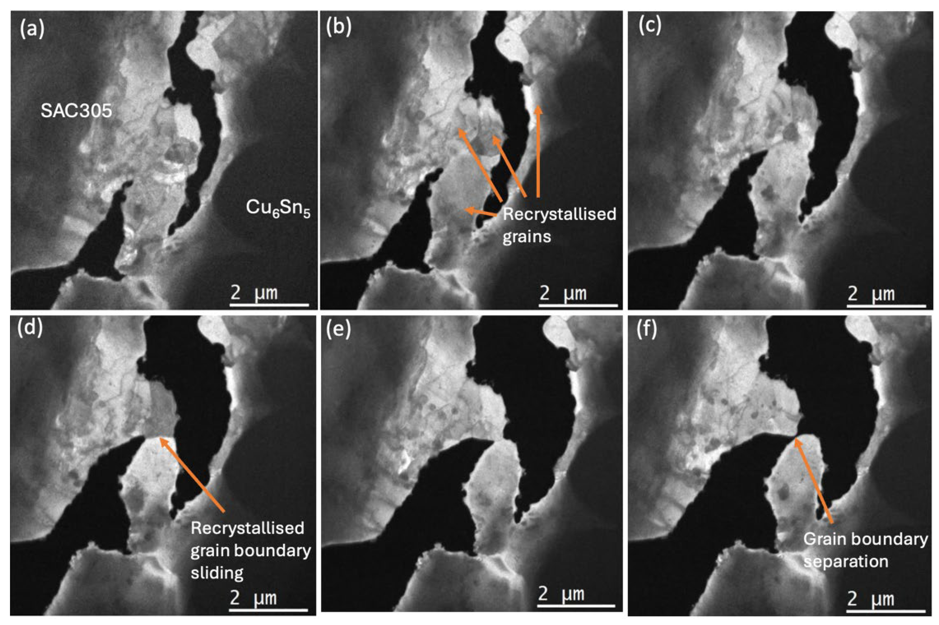
Figure 8.
Still images from supplemental Video S2b. Higer magnification of Figure 4. Crack propagation with recrystallised grain boundary sliding.
Figure 8.
Still images from supplemental Video S2b. Higer magnification of Figure 4. Crack propagation with recrystallised grain boundary sliding.
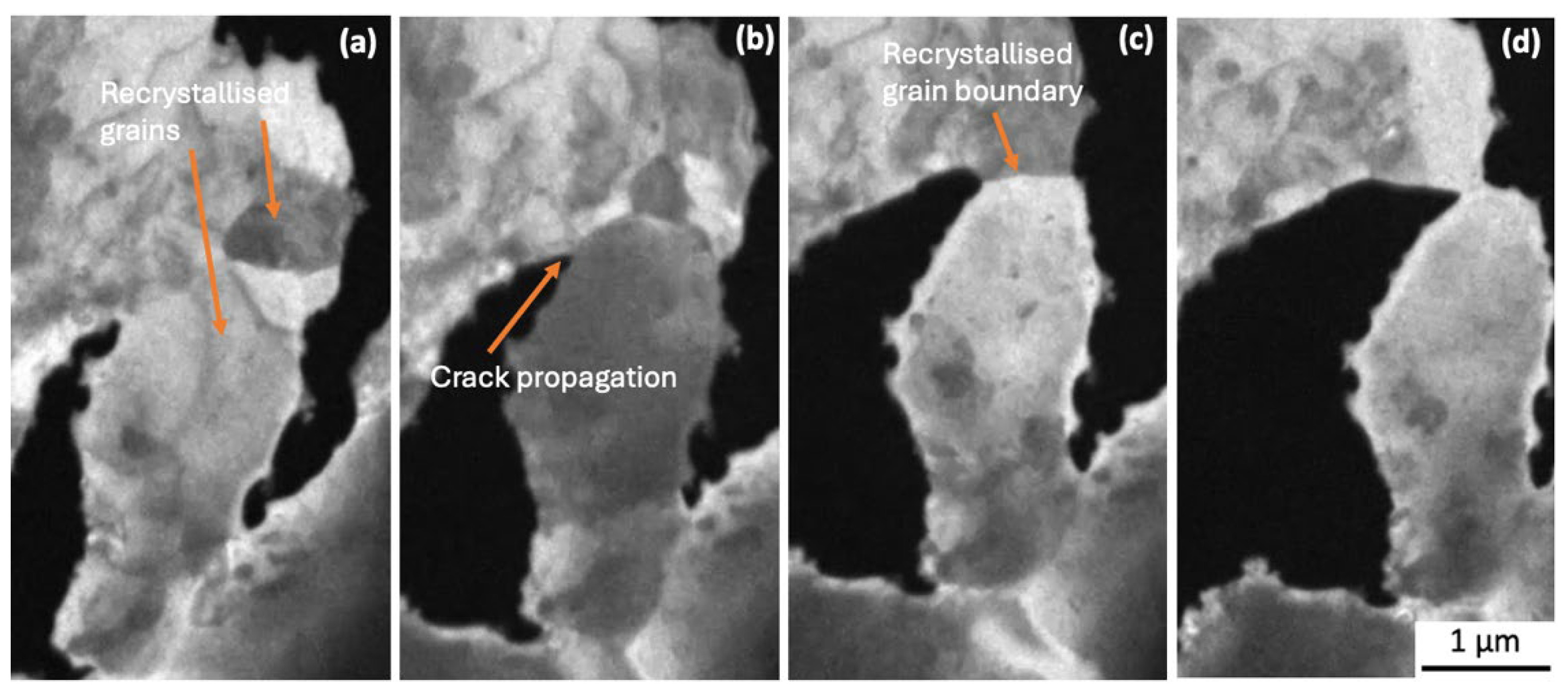
Figure 9.
Energy-filtered TEM images of recrystallised grains after total separation during testing. (a) Low magnification, and (b) higher magnification of square marked region of (a). Recrystallised grains containing some Ag3Sn particles.
Figure 9.
Energy-filtered TEM images of recrystallised grains after total separation during testing. (a) Low magnification, and (b) higher magnification of square marked region of (a). Recrystallised grains containing some Ag3Sn particles.
Disclaimer/Publisher’s Note: The statements, opinions and data contained in all publications are solely those of the individual author(s) and contributor(s) and not of MDPI and/or the editor(s). MDPI and/or the editor(s) disclaim responsibility for any injury to people or property resulting from any ideas, methods, instructions or products referred to in the content. |
© 2025 by the authors. Licensee MDPI, Basel, Switzerland. This article is an open access article distributed under the terms and conditions of the Creative Commons Attribution (CC BY) license (http://creativecommons.org/licenses/by/4.0/).
Copyright: This open access article is published under a Creative Commons CC BY 4.0 license, which permit the free download, distribution, and reuse, provided that the author and preprint are cited in any reuse.


