
Submitted:
07 July 2025
Posted:
09 July 2025
You are already at the latest version
Abstract
The Bi-Sn, Bi-Sn-Ag, and Bi-Sn-Sb solder alloy systems represent lead-free, environmentally friendly alternatives for reliable electronic assembly. These alloys comply with increasingly strict environmental and health regulations, while offering low melting points suitable for soldering temperature-sensitive components. The addition of Ag or Sb improves mechanical strength, hardness, wear resistance, and thermal stability. Microstructural analysis confirmed homogeneous, defect-free surfaces. Comprehensive microstructural characterization using optical microscopy, SEM, EDS, and BSE imaging revealed refined, heterogeneous microstructures with distinct phase segregation. Dendritic growth, eutectic formations, and intermetallic compounds were observed. Sb addition promoted granular intermetallics, while Ag induced needle-like precipitates along phase boundaries. EDS confirmed expected compositions, and BSE imaging enhanced contrast between Bi-, Sn-, Sb-, and Ag-rich regions. The study also reports the thermal and electrical conductivities of Bi60Sn40, Bi60Sn35Ag5, and Bi60Sn35Sb5 alloys over the 25–140 °C range. Bi60Sn40 showed an increase in thermal conductivity from 16.93 to 26.93 W/m·K, while Bi60Sn35Ag5 reached 18.28 W/m·K at 25 °C, and Bi60Sn35Sb5 exhibited 13.89 W/m·K. These findings underline the critical influence of alloying elements on microstructure, phase stability, and thermophysical behavior, supporting their application in low-temperature soldering technologies.
Keywords:
Bi-Sn based alloys
; Ag and Sb additions
; optical microscopy
; SEM-EDS
; BSED
; low-temperature soldering
; environmental-friendly materials
1. Introduction
The rapid progress of the electronics industry has increasingly underscored the need for materials that are not only efficient and reliable but also environmentally sustainable [1]. As consumer electronics continue to shrink in size and grow in complexity, the demand for high-performance interconnection technologies has intensified accordingly [2]. At the core of this field lies the selection and optimization of soldering materials, which are essential for ensuring robust electrical and mechanical connections within electronic assemblies [3].
For many years, lead-based solders—particularly Sn-Pb alloys—dominated electronics manufacturing due to their suitable melting points, excellent wetting characteristics, and well-established long-term reliability [4,5,6]. However, growing concerns about the toxic effects of lead on both human health and the environment have prompted extensive regulatory efforts to reduce or eliminate its use. The most prominent of these is the Restriction of Hazardous Substances (RoHS) Directive adopted by the European Union, which prohibits the use of lead in most electronic equipment. As a result, considerable research has been dedicated to identifying and developing lead-free solder alternatives capable of delivering equivalent or enhanced performance [7,8,9].
Among the most promising families of lead-free solders are bismuth-tin (Bi-Sn) binary alloys. These materials offer several notable advantages, including relatively low melting points (typically between 138–170 °C, depending on composition), low toxicity, good wettability, and excellent compatibility with standard surface-mount technology (SMT) processes [10,11,12,13]. Their capacity to facilitate low-temperature soldering is especially beneficial for thermally sensitive components such as sensors, LEDs, and polymer-based substrates. In addition, Bi-Sn alloys exhibit minimal intermetallic compound formation and provide stable joint performance under thermal cycling, making them well-suited for high-density electronic packaging applications [14,15,16,17].
Beyond these advantages, Bi-Sn alloys are also noted for their environmental friendliness and their excellent performance in specific applications, such as flexible printed circuits, components mounted on polymer substrates or optoelectronic applications. At the same time, in the context of recent trends in the electronics industry – such as 3D integration, advanced miniaturization and increasing requirements for long-term reliability – a much more detailed evaluation of ternary compositions is required, which can provide a balance between mechanical properties, soldering behavior and thermal stability [11,18,19,20,21,22].
Despite their many advantages, Bi-Sn binary alloys also present certain limitations, particularly regarding mechanical performance. Pure Bi-Sn solders are inherently brittle and exhibit low tensile strength and ductility, which poses challenges for applications subject to mechanical stress, vibration, or thermal fatigue [11]. To address these shortcomings, researchers have investigated the incorporation of additional alloying elements such as silver (Ag), antimony (Sb), copper (Cu), and indium (In), each of which can significantly influence the alloy’s microstructure, phase formation, and resulting mechanical and thermal characteristics [23,24,25,26,27].
Silver (Ag) is particularly well known for enhancing both the strength and electrical conductivity of solder joints. When introduced into Bi-Sn alloys in small concentrations (typically 1–5 wt.%), Ag contributes to grain refinement, improves thermal stability, and increases resistance to creep and fatigue. Moreover, its presence promotes the formation of advantageous intermetallic compounds that strengthen the alloy matrix without excessively compromising ductility [17,24,25,26,27,28,29,30,31,32,33,34,35]. Conversely, antimony (Sb) exerts a solid solution strengthening effect, improving hardness and wear resistance while also enhancing oxidation resistance during soldering. The addition of Sb to Bi-Sn alloys has been shown to enhance dimensional stability and thermal cycling resistance—properties critical for reliable performance in modern electronic assemblies [10,11,14,17,26,36].
Alloys composed of bismuth (Bi), tin (Sn), and antimony (Sb) are widely utilized in various technological applications due to their distinctive combination of properties. A representative system within this category is the Bi-Sn-Sb ternary alloy, typically formulated with varying proportions of the three elements to tailor specific performance characteristics. These alloys are valued for their relatively low melting points, high electrical conductivity, and reduced toxicity compared to conventional heavy-metal-based systems. Additionally, the incorporation of Sb enhances the mechanical strength and thermal stability of the alloy, making Bi-Sn-Sb systems attractive candidates for lead-free soldering, thermoelectric devices, and low-temperature fusing applications [14,17,26,36,37].
Building on the advantages of Bi-Sn and Bi-Sn-Sb alloys, further enhancement in performance can be achieved through the addition of other alloying elements such as silver (Ag), resulting in ternary systems like Bi-Sn-Ag. The use of bismuth-based alloys, particularly those with lower melting points, represents an effective strategy for minimizing thermal damage during soldering processes. These alloys help mitigate common defects such as delamination or “pop-corning” in moisture-sensitive components. Among the primary alloying elements for tin, bismuth and indium are frequently employed, with bismuth offering a more cost-effective alternative [24,27,28,29,38].
Despite their recognized advantages, the successful application of Bi-Sn-Sb and Bi-Sn-Ag ternary alloys necessitates a more comprehensive understanding of their microstructural evolution, compositional homogeneity, and phase transformations during solidification. The behavior of these alloys throughout casting, cooling, and thermal exposure plays a critical role in determining their long-term performance and reliability. Furthermore, factors such as compositional fluctuations, contamination, or inconsistencies in processing can lead to defects including porosity, elemental segregation, or the formation of undesirable intermetallic phases [19,21,22,28,30,31,36,37,39,40,41].
To evaluate and optimize the performance of such solder systems, comprehensive characterization is crucial. Microstructural analysis through optical microscopy offers a general assessment of grain structure and phase distribution, facilitating the detection of casting defects, micro-segregation, and solidification patterns. For more detailed investigation, scanning electron microscopy (SEM), typically combined with energy-dispersive X-ray spectroscopy (EDS), provides high-resolution imaging and elemental mapping at the microscale. These advanced techniques are essential for examining the influence of alloying additions on eutectic morphology, the spatial distribution and nature of intermetallic compounds, and the overall structural integrity of the solder matrix.
This study aims to investigate the microstructural and chemical characteristics of Bi-Sn-based solder alloys with controlled additions of silver (Ag) and antimony (Sb). Three alloy compositions are examined: a binary Bi60Sn40 alloy serving as the base reference and two ternary systems—Bi60Sn35Sb5 and Bi60Sn35Ag5. Each alloy undergoes a series of metallographic, compositional, and mechanical analyses to evaluate the influence of alloying content on structural evolution and mechanical performance. By establishing clear structure–property relationships in Bi-Sn-based solders modified with Sb and Ag, this research provides valuable insights into the design of advanced lead-free solder materials. The findings support the development of high-reliability interconnection solutions for electronic applications and offer a foundation for optimizing both processing methods and alloy composition.
2. Materials and Methods
The preparation of the solder alloys involved a controlled series of steps to ensure desirable physic-chemical properties. High-purity raw materials were used: Bi (98.9%), Sn (99.6%), Ag (99.9%), and Sb (99.9%), selected for their favorable behavior in low-temperature soldering applications.
Melting and casting were performed in graphite and magnesite crucibles—chosen for their chemical resistance and high refractoriness. A protective and refining flux composed of NH₄Cl and KCl in a 1:4 ratio was used to minimize oxidation and improve alloy quality.
The flux was added in three equal portions during melting to limit air contact and preserve alloy purity. All raw materials and flux components were weighed using a precision electronic balance.
The process was carried out under normal atmospheric conditions in three stages:
- Bi-Sn alloy: Furnace set at 300 °C (peak 320 °C due to ±20 °C tolerance). After thermal stabilization, pre-weighed Bi and Sn were introduced.
- Bi-Sn-Sb alloy: Furnace set at 650 °C (peak 670 °C). After stabilization, Sb was added to the pre-melted Bi-Sn matrix.
- Bi-Sn-Ag alloy: Furnace set at 980 °C (peak 1000 °C). Ag was melted first, followed by the addition of Bi and Sn.
The molten alloy was held for approximately one minute to reduce losses from oxidation and evaporation, then cast into molds.
Given the novelty of the alloy compositions, detailed chemical analyses were conducted to accurately determine the content of major and trace elements, including potential impurities introduced from the raw materials. This information is critical to assess and predict solder behaviors such as adhesion, wettability, and electrical conductivity—and identify any elements that might negatively affect performance. The analytical method was selected based on its sensitivity, detection limits, and suitability for characterizing solder alloys.
The chemical characterization was performed using the Z-200 portable metal and alloy analyzer (LIBS Sci Aps), equipped with an integrated argon purge system for improved accuracy. Its advanced technology includes an integrated argon purge to provide more accurate results. Laser surface cleaning virtually eliminates surface preparation. Laser scanning of impact points greatly increases the accuracy of the analysis. The Z-200 portable analyzer is perfectly suited for in-situ analysis of metals and alloys.
For microstructural investigations, metallographic specimens were prepared by sectioning, mounting, grinding, fine grinding, polishing, etching with a H2O2 (30%): H2O mixture. The optical microscopy analysis was performed with the Axio Imager A1m optical microscope (Carl Zeiss, Germany), equipped with a digital camera Canon Power Shot A 640, digital Zoom 10X and image processing software Axio Vision Release 4.8. The scanning electron microstructural characterization was conducted using the FEI QUANTA 250 (FEI Company, Hillsboro, OR USA), in high vacuum mode, backscattered electron techniques (BSE) using an Angular Backscattered Detector. Point analysis, elemental mapping, and semi-quantitative analysis were carried out using energy-dispersive X-ray spectroscopy (EDS) with the EDAX ELEMENT EDS Analysis System, which includes a fixed Silicon Drift Detector (SDD) and the ELEMENT EDS Analysis Software Suite (EDAX APEX™, Digital Micrograph 3.6).
The thermal conductivity of the investigated Bi-Sn-based solder alloys (Bi60Sn40, Bi60Sn35Ag5, Bi60Sn35Sb5) was determined using the Netzsch LFA 457 Micro Flash system, a high-precision thermal analyzer widely used for solid material characterization. This instrument operates based on the Laser Flash Analysis (LFA) method, where a short-duration energy pulse is applied to one surface of a disc-shaped sample. The temperature rise on the opposite surface is recorded over time by an infrared detector, allowing for accurate calculation of thermal diffusivity. Thermal conductivity (λ) was then calculated using the relation:
where α is the thermal diffusivity (m2/s), ρ is the density (kg/m³), and Cp is the specific heat capacity (J/kg·K). The system operates over a wide temperature range (–125 °C to +1100 °C), making it suitable for low-melting solder alloys. Measurements were performed from 25 °C to 140 °C.
λ = α ⋅ ρ ⋅ Cp,
The electrical resistivity of the investigated Bi-Sn-based solder alloys was measured using a Signatone four-point probe system, mounted on a precision measurement station. The technique applies a constant current of 5 mA through the two outer probes, while the voltage drop (~2.5 mV) is measured across the two inner probes. The probe spacing was 1 mm, following the standard Signatone configuration. The sample was placed on a flat platform, and tungsten probes were brought into controlled contact with the alloy surface under a constant force to ensure reproducibility. The resistivity (ρₑ) was calculated from the measured values, and the electrical conductivity (σ) was obtained using the inverse relation:
σ = 1 / ρe,
This method minimizes contact resistance effects and ensures reliable, repeatable measurements for solid metallic samples.
3. Results and Discussion
Following optical and SEM-EDS analyses, it was found that all three compositions (Bi60Sn40, Bi60Sn35Sb5 and Bi60Sn35Ag5) present a homogeneous structure with well-distributed phases, which indicates an efficient elaboration and casting process. The presence of Sb led to the formation of Sn-Sb intermetallic compounds uniformly dispersed in the eutectic matrix, which contributes to structural strengthening. The addition of Ag contributed to the formation of a lamellar-globular structure, suggesting a structure close to the eutectic point, with excellent bonding potential. No major defects such as porosity, microcracks or delamination in critical areas were observed.
The investigated Bi-Sn-based solder alloys exhibited temperature-dependent thermal and electrical properties influenced by their composition. Thermal conductivity decreased with increasing temperature for all alloys, while the addition of 5% Ag in Bi60Sn35Ag5 significantly enhanced thermal conductivity. Bi60Sn35Sb5 demonstrated intermediate thermal values. Electrical resistivity increased with temperature, consistent with typical metallic behavior, with Bi60Sn35Ag5 showing lower resistivity compared to the other alloys studied.
3.1. Characterization of Bi-Sn Based Solder Alloys
3.1.1. Chemical Composition
The chemical composition of the Bi-Sn-based solder alloys (Bi60Sn40, Bi60Sn35Sb5, and Bi60Sn35Ag5), determined by laser-induced spectrometry, is summarized in Table 1. The measured elemental concentrations are consistent with nominal formulations, with slight deviations attributable to processing or minor impurities.
Sample Bi60Sn40 presents a near-binary composition, with Bi at 59.437 wt.% and Sn at 39.475 wt.%. Trace amounts of Sb (0.0167%), Cu (0.122%), and Fe (0.018%) are also detected, likely resulting from raw material impurities or contact with processing equipment. Sample Bi60Sn35Sb5 contains 4.88 wt.% Sb, closely matching the intended 5% addition. The Sn content is slightly reduced (34.533%) due to substitution by Sb, while Bi remains nearly constant at 59.411%. Minor concentrations of Cu (0.182%) and Fe (0.029%) are again present, but within typical impurity ranges. Sample Bi60Sn35Ag5 includes 4.93 wt.% Ag, in agreement with the target composition. The Sn concentration decreases correspondingly to 34.271%, while Bi slightly decreases to 58.804%. A notably higher level of Cu (1.63%) is observed in this sample, which may influence the formation of additional intermetallic phases such as Cu6Sn5 or Ag3Sn.
3.1.2. Optical Microscopy
Optical microscopy was employed as a fundamental technique for the initial examination of the microstructure of the solder alloys studied. This method enables the visualization of phase morphology, grain structure, and solidification patterns on a micrometer scale, providing essential information regarding the homogeneity and distribution of the constituent phases. The metallographic samples were prepared using standard procedures, including grinding, polishing, and chemical etching, to reveal the microstructural features with sufficient contrast. Through optical observation, key characteristics such as dendritic growth, eutectic formations, and the presence of primary phases or intermetallic compounds were identified and documented. Although limited in resolution compared to electron microscopy, optical microstructural analysis remains a valuable and widely used approach for assessing general structural trends and for comparing the effects of compositional variations across different alloy systems. The following section presents representative optical micrographs for each alloy, accompanied by a discussion on the morphological features and phase distributions observed.
The microstructure of sample Bi60Sn40 alloy presented in Figure 1 is characteristic of rapid solidification and indicates good microstructural homogeneity. According to the literature [35,42], the observed structure is specific to compositions close to Bi70Sn30, where the reduced solubility of Bi in Sn leads to the precipitation of Bi in granular form.
The structure presented in Figure 1 consisting of two main phases, relatively evenly distributed, was observed. The light-colored (white) phase presents a granular and discontinuous morphology, typical of the tin-rich phase (β-Sn). The light gray phase/background matrix is more heterogeneous and has a larger grain size, characteristic of the bismuth-rich phase (α-Bi). The white phase presents a branched and irregular texture, with a tendency towards coalescence, indicating a slow solidification or a controlled cooling, which allowed the formation of eutectic segregation zones. No inclusions or porosity are evident, demonstrating a clean elaboration, without evident oxides. The eutectic structure is well distributed, indicating good solderability and moderate mechanical strength. Potential for applications where low solder temperature is essential (≤150°C).
The microstructure of sample Bi60Sn35Sb5 alloy is presented in Figure 2. We can observe that the addition of Sb led to the formation of stable intermetallic compounds, which contributed to the strengthening of the material. The results are consistent with the data in the specialized literature [35,42], which show the efficiency of Sb in increasing the hardness and microstructural stability.
Figure 2 shows a heterogeneous microstructure with clearly distinguishable phases. The light gray matrix represents the Bi-rich phase, which typically solidifies first and forms the continuous network. The darker gray regions with distinct lamellar or eutectic structures are likely Sn-rich phases, potentially forming a eutectic with Bi. The large grains with parallel striations suggest the presence of a primary Bi phase exhibiting growth lines or twinning, common in Bi-containing alloys.
The white or bright precipitates scattered within the microstructure could correspond to Sb-rich intermetallic compounds (e.g., Bi-Sb or Sn-Sb compounds), which form during solidification and segregate at grain boundaries or within the eutectic mixture. No visible cracks or porosity are apparent, suggesting good sample preparation and metallurgical integrity.
The microstructure presented in Figure 3 for sample (Bi60Sn35Ag5 alloy) is characteristic of Ag-modified alloys and indicates good compatibility with precision soldering applications. According to [35,42], the presence of Ag improves the thermal stability and creep resistance of Bi-Sn alloys. Sporadically, in some areas the presence of Ag inclusions is observed.
Figure 3 reveals a multiphase structure consisting of a light gray matrix rich in Bi, fine eutectic regions likely formed by Bi-Sn, visible as lamellar or granular zones and bright white, elongated or acicular structures identified as intermetallic Ag3Sn phases. The left image shows a denser cluster of Ag3Sn precipitates, suggesting localized segregation or directional solidification. The right image presents a more evenly distributed microstructure with better-defined intermetallic phases, indicating a more uniform solidification front. The presence of Ag3Sn enhances mechanical strength but may also increase brittleness, which is typical for Ag-containing solder alloys.
3.1.3. Microstructural and Compositional Analysis by SEM-EDX and BSE Imaging
A comprehensive microstructural characterization was conducted to investigate the morphological features, phase distribution, and elemental composition of the investigated solder alloys. Scanning Electron Microscopy (SEM) served as the primary tool for observing the surface morphology and identifying the microstructural constituents at different magnifications, offering detailed insights into the solidification behavior and the formation of distinct phases.
Complementary to SEM, Energy-Dispersive X-ray Spectroscopy (EDX) was employed to perform qualitative and semi-quantitative elemental analysis. Backscattered Electron (BSE) imaging was further utilized to enhance phase contrast based on atomic number differences, providing a clearer distinction between Bi-rich, Sn-rich, and intermetallic regions. The integration of these methods allows for a robust interpretation of the microstructural evolution and phase stability as influenced by alloying elements.
SEM micrographs of the Bi60Sn40 alloy at different magnifications were presented in Figure 4. The Bi60Sn40 alloy forms a typical eutectic microstructure, with Bi and Sn phases coexisting in a well-dispersed pattern.
Figure 4a captures finer details and could be observed lamellar spacing and grain boundaries. The light regions are likely the Bi-rich phase, while the darker ones correspond to the Sn-rich phase.
The relatively uniform lamellar pattern suggests homogeneous solidification with a eutectic structure. The polygonal/rectangular islands (light gray) might be primary Bi precipitates embedded in the eutectic matrix. Figure 4b provides a broader view of the microstructural distribution and highlights the coarser eutectic pattern, with more distinct phase separation. A dendritic-like Sn-rich phase can be seen growing within a Bi-rich matrix.
Energy-Dispersive X-ray Spectroscopy (EDS) analysis was performed on the Bi60Sn40 alloy to verify its elemental composition and assess the local phase chemistry. This method provides qualitative and semi-quantitative insight into the elemental distribution within the microstructure. The EDS spectrum presented in Figure 5 for the Bi60Sn40 solder alloy reveals distinct peaks corresponding to bismuth (Bi) and tin (Sn), the two principal components of the alloy. A dominant Bi peak appears near 2.45 keV, indicating a Bi-rich phase, while characteristic Sn peaks are observed around 3.4 keV and 3.7 keV, confirming the presence of Sn-rich regions. The absence of additional elemental peaks suggests that the analyzed area is representative of the main binary Bi–Sn phases, without detectable intermetallic compounds or third-element inclusions. In Table 2 presents the elemental composition of the Bi60Sn40 solder alloy obtained from EDS analysis. The data provides both weight and atomic percentages of the main constituent elements, Bi and Sn, in the analyzed microstructural region.
The EDS results show that the alloy consists of approximately 68.49 wt.% Bi and 31.51 wt.% Sn, which aligns well with the nominal Bi60Sn40 composition. The higher atomic percentage of Sn is due to its lower atomic mass relative to Bi. The peak-to-background (P/B) ratios and relative errors are within acceptable limits, confirming the reliability of the measurement. This confirms the binary nature of the solder and the homogeneous distribution of Bi and Sn in the analyzed area.
In Figure 6, the backscattered electron (BSE) imaging combined with elemental mapping via EDS was employed to visualize the distribution of the main alloying elements in the Bi60Sn40 solder alloy. This technique provides compositional contrast and spatial resolution, highlighting regions of varying atomic number and allowing for phase discrimination based on elemental enrichment.
Figure 6 displays a set of BSE and elemental mapping images for the Bi60Sn40 solder alloy. Figure 1a presents the BSE microstructure, revealing compositional contrast across different phases. Figure 6b shows the superimposed elemental map with Sn in yellow and Bi in red. Figure 6c, the tin (Sn) distribution dominates, uniformly covering the matrix (yellow), which is consistent with its higher atomic percentage. Figure 6d illustrates the distribution of bismuth (Bi), concentrated in smaller, dispersed regions, appearing in red. The maps indicate a heterogeneous microstructure, with Bi-rich areas embedded within a Sn-rich matrix.
SEM micrographs of the Bi60Sn35Sb5 alloy at different magnifications were presented in Figure 7. The microstructure indicates solidification with phase segregation, common in multicomponent solder systems. The addition of 5 wt.% Sb leads to the formation of dispersed intermetallic phases, which can refine the microstructure and potentially enhance strength and thermal stability. Primary Bi grains form first due to Bi’s high melting point, while Sn and Sb form eutectic or intermetallic structures in the residual melt. Figure 7a shows a heterogeneous microstructure with large Bi-rich primary phases (bright gray) embedded in a matrix.
The darker areas surrounding the Bi-rich grains are likely Sn-rich eutectic regions. Small dispersed dark particles throughout the matrix may represent Sb-containing intermetallic or precipitates. The structure indicates partial solidification of primary Bi followed by eutectic transformation during cooling. Figure 7b displays a large primary Bi grain (bright) with a central Sb-rich particle or segregated region, possibly an intermetallic compound (dark central core). The surrounding area contains a finer distribution of small dark particles, likely Sb-based intermetallic (e.g., Bi-Sb or Sn-Sb compounds). This suggests segregation of Sb during solidification, forming discrete phases rather than a continuous solid solution.
EDS (Energy-Dispersive X-ray Spectroscopy) analysis was performed on the Bi60Sn35Sb5 solder alloy to identify and confirm the elemental constituents within the microstructure. This method provides valuable insight into the local chemical composition and distribution of alloying elements. The EDS spectrum presented in Figure 8 for the Bi60Sn35Sb5 alloy displays prominent peaks corresponding to bismuth (Bi) and tin (Sn), which are the base components of the alloy. Additionally, a distinct peak attributed to antimony (Sb) is observed near 3.8 keV, confirming the successful incorporation of Sb into the alloy matrix. The intense Bi peak around 2.48 keV and the characteristic Sn peaks in the range of 3.4–3.7 keV indicate a multi-phase microstructure where Sb is likely present in solid solution or in intermetallic compounds with Sn or Bi.
Table 3 presents the elemental composition of the Bi60Sn35Sb5 solder alloy as determined by Energy-Dispersive X-ray Spectroscopy (EDS). The analysis provides quantitative data in terms of both weight and atomic percentages for the main alloying elements: Bi, Sn, and Sb.
The EDS results confirm the presence of all three targeted elements in the Bi60Sn35Sb5 alloy. Bismuth (Bi) is the dominant component at 69.93 wt.%, followed by tin (Sn) at 20.20 wt.%, and antimony (Sb) at 9.87 wt.%. These values are in good agreement with the intended nominal composition. The relatively high atomic percentage of Sn (29.05%) reflects its lower atomic mass. The net intensity values, and peak-to-background (P/B) ratios indicate strong signal quality, and error margins are acceptable, supporting the accuracy of the measurements.
To evaluate the elemental distribution and phase separation in the Bi60Sn35Sb5 solder alloy, backscattered electron (BSE) imaging coupled with energy-dispersive X-ray spectroscopy (EDS) mapping was conducted (Figure 9). This combined technique provides insight into the spatial distribution of Sn, Bi, and Sb within the microstructure. Figure 9 presents BSE and EDS mapping images of the Bi60Sn35Sb5 alloy. Figure 9a shows the BSE microstructure, highlighting compositional contrasts among different phases. In Figure 9b, the overlapped elemental map visualizes Sn (yellow), Bi (red), and Sb (green). Figure 9c reveals that Sn is predominantly distributed in the matrix, forming a continuous phase. Figure 9d shows Bi-rich regions that appear more localized and concentrated and Figure 9e indicates a uniform but somewhat dispersed presence of Sb, primarily located around or between the Sn and Bi phases. The elemental maps confirm a heterogeneous distribution, with each element forming distinct microstructural domains.
The SEM micrographs presented in Figure 10 correspond to the Bi60Sn35Ag5 solder alloy at different magnifications, revealing a complex multiphase microstructure. The microstructure in Figure 10a exhibits a dendritic or eutectic-like matrix, likely composed of Bi-rich and Sn-rich phases. A notable feature is the presence of elongated and interconnected intermetallic compounds (IMCs), prominently oriented along specific crystallographic directions. These IMCs are characteristic of Ag3Sn, formed due to the interaction between Ag and Sn during solidification. The uniform distribution of these phases suggests a relatively homogeneous alloy structure. Figure 10b provides a more detailed view of the IMCs, which appear as long, rod-like or needle-shaped structures embedded in the eutectic matrix. These features are consistent with Ag3Sn intermetallic, which tend to form as elongated precipitates. The surrounding matrix exhibits fine lamellar or granular morphology, indicative of a eutectic reaction between Bi and Sn.
The presence of Ag3Sn contributes to improved mechanical strength and thermal stability, but its morphology and distribution must be controlled to avoid embrittlement. The observed structure confirms that Ag addition significantly alters the microstructure by promoting intermetallic formation and refining the eutectic structure.
To assess the elemental distribution within the Bi60Sn35Ag5 solder alloy, Energy-Dispersive X-ray Spectroscopy (EDS) was conducted. This method allows for the identification and semi-quantitative estimation of the alloy’s constituent elements based on their characteristic X-ray emission peaks. The EDS spectrum shown in Figure 11 presents the dominant peaks corresponding to tin (Sn), which is the major component in the selected region.
A significant silver (Ag) peak is also observed near 3.0 keV, indicating the successful incorporation of Ag into the alloy matrix. Two distinct peaks of bismuth (Bi) are present, though with lower intensity, suggesting a relatively low local concentration. The peak distribution confirms the presence of all intended alloying elements, supporting the results obtained from bulk compositional analysis.
Table 4 presents the elemental composition of the Bi60Sn35Ag5 solder alloy obtained through EDS. The analysis provides detailed data on the weight and atomic percentages of the main constituent elements: Sn, Ag, and Bi.
The EDS results indicate a high content of tin (Sn) at 68.09 wt.%, followed by silver (Ag) at 25.82 wt.%, and a minor amount of bismuth (Bi) at 6.09 wt.%. It should be noted that these values reflect local compositional analysis of a microstructural region rich in Ag3Sn phases, not the bulk alloy composition. The low atomic percentage of Bi (3.32%) aligns with its higher atomic mass. Despite Bi being a major base component in the nominal alloy, its low detection here suggests localized sampling or microstructural segregation. The strong net intensity and peak-to-background (P/B) ratio for Sn and Ag confirm reliable detection, while the high error percentage for Bi reflects lower signal strength. These values are consistent with the microstructural complexity introduced by the addition of Ag.
To gain insight into the elemental distribution and microstructure of the Bi60Sn35Ag5 solder alloy, a backscattered electron (BSE) imaging technique combined with energy-dispersive X-ray spectroscopy (EDS) mapping was employed and the results were presented in Figure 12. This approach enables the identification of Sn-, Bi-, and Ag-rich phases and reveals compositional segregation at the microscale. Figure 12a shows the overall BSE micrograph, where heavier elements such as Bi and Ag appear brighter due to their higher atomic numbers. Figure 12b presents the elemental distribution overlay, indicating Sn in yellow (65%), Bi in red (35%), and Ag in blue (22%). Individual maps of Sn, Bi, and Ag are displayed in Figure 12 (c), Figure 12 (d), and Figure 12 (e), respectively. Notably, Ag appears as distinct acicular, or needle-like precipitates aligned along phase boundaries. These detailed mapping aids in understanding the alloy’s phase morphology and elemental homogeneity, which are crucial for its mechanical and thermal performance.
The microstructural characterization of the Bi60Sn40, Bi60Sn35Sb5, and Bi60Sn35Ag5 solder alloys using optical microscopy, SEM, EDS, and BSE imaging revealed significant insights into their morphology and elemental distribution. Optical and SEM images showed a refined and heterogeneous microstructure, with visible segregation of phases and intermetallic compounds, especially in the doped alloys. EDS analysis confirmed the expected elemental composition in each alloy, with minor deviations due to localized phase enrichment. The BSE images highlighted contrast differences corresponding to the presence of Bi-, Sn-, Sb-, and Ag-rich regions, depending on the alloy. In particular, the addition of Sb and Ag led to the formation of well-defined intermetallic compounds—Sb promoted granular structures, while Ag formed needle-like precipitates aligned along phase boundaries. These findings suggest that alloying elements significantly influence the microstructure, phase distribution, and potential mechanical performance of the solder materials.
3.2. Thermal and Electrical Conductivity of Bi-Sn Based Solder Alloys
The thermal and electrical conductivities of the Bi60Sn40, Bi60Sn35Ag5, and Bi60Sn35Sb5 alloys were systematically evaluated to understand their thermophysical behavior across a temperature range of 25 °C to 140 °C. The dataset in Table 5 presents a detailed temperature-dependent evaluation of thermal diffusivity (α), thermal conductivity (λ), electrical resistivity (ρ), and electrical conductivity (σ) for three Bi-Sn-based solder alloys. Bi60Sn40 alloy shows the highest thermal conductivity values across the full temperature range, rising from 16.93 W/m·K at 25°C to 26.93 W/m·K at 140°C, likely due to its simpler binary composition with fewer scattering centers suggesting enhanced phonon and electron transport as temperature rises. Alloys Bi60Sn35Ag5 and Bi60Sn35Sb5 exhibit a clear decline in thermal conductivity with increasing temperature, a typical behavior at elevated temperatures. The addition of Ag slightly reduced λ in Bi60Sn35Ag5, starting from 18.28 W/m·K to 16.77 W/m·K at 140°C indicating that silver addition may introduce scattering centers or phase boundaries that hinder heat conduction.
In contrast, Bi60Sn35Sb5 exhibited the lowest λ, decreasing from 13.90 W/m·K to 10.66 W/m·K, indicating that Sb impairs thermal transport more significantly, likely due to its effect on phonon scattering and microstructural complexity. Electrical resistivity increases with temperature across all alloys, consistent with the classical metallic behavior where lattice vibrations impede electron flow at higher temperatures. Bi60Sn40 exhibits increasing electrical resistivity from 3.80·10⁻⁷ Ω·m to 8.35·10⁻⁷ Ω·m, and a corresponding decrease in conductivity from 2.63·10⁶ S/m to 1.20·10⁶ S/m as temperature increases—expected behavior due to enhanced phonon scattering. Bi60Sn35Ag5 starts with a very low resistivity (1.52·10⁻⁷ Ω·m) and high electrical conductivity (6.54·10⁶ S/m) at 25°C. Although σ decreases slightly with temperature, it remains the highest among all alloys, indicating that Ag significantly enhances electrical transport. Bi60Sn35Sb5 shows similar electrical performance to the Ag-containing alloy at 25°C, with σ = 6.52·10⁶ S/m, but its conductivity decreases more significantly with temperature, reaching 4.79·10⁶ S/m at 140°C. This suggests that Sb has a moderately positive impact on σ at low temperatures, but less thermal stability than Ag.
The data demonstrates that alloying with Ag or Sb enhances electrical conductivity significantly compared to the base Bi60Sn40 alloy. However, Ag provides a better balance between thermal and electrical performance, while Sb tends to degrade thermal conductivity more sharply. These combined thermal and electrical characterizations highlight the significant impact of alloying elements on the solder alloys’ performance, providing critical data for optimizing low-temperature soldering processes in electronic applications.
5. Conclusions
Bi-Sn-based solder alloys, particularly when modified with small additions of elements such as Sb and Ag, represent a promising class of lead-free alternatives due to their favorable microstructural characteristics, good elemental distribution, and adaptability. These alloys offer a balance between environmental compliance and functional performance, making them suitable candidates for electronic and thermal applications where lead elimination is essential. The addition of alloying elements such as Sb and Ag to the Bi60Sn40 base alloy leads to significant microstructural modifications, promoting the formation of distinct intermetallic phases that are clearly observable through SEM and BSE imaging. These microstructural changes are expected to influence the mechanical and thermal behavior of the solder alloys. EDS and BSE analyses confirmed a uniform elemental distribution in the base Bi60Sn40 binary alloy, while the ternary alloys (Bi60Sn35Sb5 and Bi60Sn35Ag5) exhibited localized concentrations of Sb and Ag, respectively. This indicates the potential of minor alloying additions to tailor phase formation and to improve the performance of lead-free solder materials.
The study demonstrates that alloying Bi-Sn solder alloy with Ag and Sb significantly influences their thermal and electrical properties. Although Ag slightly reduces thermal conductivity at higher temperatures, it provides superior electrical conductivity and overall thermal stability compared to Sb. However, both alloying components increase electrical resistivity relative to the binary alloy, reflecting complex microstructural effects. These findings offer valuable insights into the development of next-generation lead-free solders in advanced electronic packaging technologies.
Author Contributions
Conceptualization, A.-A.I., F.N. and G.I.; Data curation, A.-A.I., F.N., G.I. and I.P.; Formal analysis, A.-A.I., F.N., G.I., I.P., F.M., R.B., D.-V.D., A.-C.M., M.G., A.P. and C.U.; funding acquisition, A.-A.I. and R.B.; Investigation, F.N., G.I., I.P., F.M., D.-V.D., A.-C.M., M.G., A.P., and C.U.; Methodology, F.N., G.I., I.P., and F.M.; Project administration, F.N. and G.I.; Resources, A.-A.I., F.N., G.I., and R.B.; Software, A.-A.I., F.N., G.I., I.P., F.M., R.B., D.-V.D., A.-C.M., M.G., A.P. and C.U.; Supervision, F.N. and G.I.; Validation F.N., G.I.; Visualization A.-A.I., F.N. and G.I.; Writing—original draft, A.-A.I., F.N. and G.I.; Writing—review & editing, F.N., G.I., and I.P.; All authors have read and agreed to the published version of the manuscript.
Funding
This research received no external funding.
Institutional Review Board Statement
Not applicable.
Informed Consent Statement
Not applicable.
Data Availability Statement
Data are contained within the article.
Conflicts of Interest
The authors declare no conflicts of interest.
References
- Balakrishnan, R.B.; Anand, K.P.; Chiya, A.B. Electrical and electronic waste: a global environmental problem. Waste Manag. Res. 2007, 25, 307–318. [Google Scholar] [CrossRef]
- Apurva, G.; Snehal, M.; Girish, R.P. An Overview of Digital Transformation and Environmental Sustainability: Threats, Opportunities, and Solutions. Sustainability 2024, 16, 11079. [Google Scholar] [CrossRef]
- Althaf, S.; Babbitt, C.W. Disruption risks to material supply chains in the electronics sector. Resour. Conserv. Recycl. 2021, 167, 105248. [Google Scholar] [CrossRef]
- Abtew, M.; Selvaduray, G. Lead-free Solders in Microelectronics. Mater. Sci. Eng.: R.: Rep. 2000, 27, 95–141. [Google Scholar] [CrossRef]
- Zhang, L.; Xue, Sb.; Gao, Ll.; et al. Development of Sn–Zn lead-free solders bearing alloying elements. J. Mater. Sci. Mater. Electron. 2009, 21, 1–15. [Google Scholar] [CrossRef]
- Choi, S.; Lim, S.; Hanifah, M.M.M.; Matteini, P.; Yusoff, W.Y.W.; Hwang, B. An Introductory Overview of Various Typical Lead-Free Solders for TSV Technology. Inorganics 2025, 13, 86. [Google Scholar] [CrossRef]
- EEA – European Environment Agency. European zero pollution dashboards Progress in regulating lead (Signal). Available online: https://www.eea.europa.eu/en/european-zero-pollution-dashboards/indicators/progress-in-regulating-lead-signal (accessed on 12 June 2025).
- EUR-Lex. Document 52023SC0760, COMMISSION STAFF WORKING DOCUMENT EVALUATION of Directive 2011/65/EU on the restriction of the use of certain hazardous substances in electrical and electronic equipment Accompanying the document REPORT FROM THE COMMISSION TO THE EUROPEAN PARLIAMENT, THE COUNCIL, THE EUROPEAN ECONOMIC AND SOCIAL COMMITTEE AND THE COMMITTEE OF THE REGIONS on the review of the Directive on the restriction of the use of certain hazardous substances in electrical and electronic equipment, SWD/2023/760 final. Available online: https://eur-lex.europa.eu/legal-content/EN/TXT/?uri=SWD%3A2023%3A760%3AFIN (accessed on 12 June 2025).
- Ho, K. Understanding RoHS (Restriction of Hazardous Substances) Compliance: A Comprehensive Guide. Nemko. 2024. Available online: https://www.nemko.com/blog/rohs-explained-a-comprehensive-guide (accessed on 12 June 2025).
- Razak, N.R.A.; Salleh, M.A.A.M.; Saud, N.; Said, R.M.; Ramli, M.I.I. Influence of Bismuth in Sn-Based Lead-Free Solder – A Short Review. Solid State Phenom. 2018, 273, 40–45. [Google Scholar] [CrossRef]
- Kang, H.; Rajendran, S.H.; Jung, J.P. Low Melting Temperature Sn-Bi Solder: Effect of Alloying and Nanoparticle Addition on the Microstructural, Thermal, Interfacial Bonding, and Mechanical Characteristics. Metals 2021, 11, 364. [Google Scholar] [CrossRef]
- Koleňák, R.; Provazník, M.; Kostolný, I.; Kar, A. Soldering by the Active Lead-Free Tin and Bismuth-Based Solders. In Lead Free Solders; Kar, A., Ed.; IntechOpen, 2018. [Google Scholar] [CrossRef]
- Vianco, P.T.; Rejent, J.; Grant, R. Development of Sn-Based, Low Melting Temperature Pb-Free Solder Alloys. Mater. Trans. 2004, 45, 765–775. [Google Scholar] [CrossRef]
- Ribas, M.; Kumar, A.; Kosuri, D.; Rangaraju, R.R.; Choudhury, P.; Suresh, S.; Sarkar, S. Low temperature soldering using Sn-Bi alloys. Proceedings of SMTA International, Rosemont, IL, USA, Date of Conference (17-21 September 2017). [Google Scholar]
- Hashim, M.S.; Osman, S.A.; Efzan, E. The Development of Low-Temperature Lead-Free Solders using Sn-Bi Solders Alloys. Int. J. Recent Technol. Eng. 2019, 8, 11956–11962. [Google Scholar] [CrossRef]
- Zhang, P.; Xue, S.; Liu, L.; Wang, J.; Tatsumi, H.; Nishikawa, H. Influence of Isothermal Aging on Microstructure and Shear Property of Novel Epoxy Composite SAC305 Solder Joints. Polymers 2023, 15, 4168. [Google Scholar] [CrossRef] [PubMed]
- Shen, Y.A.; Chen, F.Y.; Gao, R.; Ho, C.E.; Nishikawa, H.; Chen, C.M. Effect of Bi Addition on Melting Behavior, Solder Joint Strength, and Thermal Aging Resistance of Sn-3.5Ag/Cu Joints. JOM 2025, 77, 4206–4214. [Google Scholar] [CrossRef]
- Straubinger, D.; Khan, Z.; Koltay, P.; Zengerle, R.; Kartmann, S.; Shu, Z. Additively Manufactured Flexible Electronics with Selectively Soldered Surface-mounted Devices Utilising StarJet Technology. IEEE 10th Electronics System-Integration Technology Conference (ESTC), Berlin, Germany, Date of Conference (11-13 September 2024). [Google Scholar] [CrossRef]
- Zhang, S.; Li, Z.; Zhou, H.; Li, R.; et al. Challenges and recent prospectives of 3D heterogeneous integration. e-Prime - Adv. Electr. Eng. Electron. 2022, 2, 100052. [Google Scholar] [CrossRef]
- Lau, J.H. Recent Advances and New Trends in Nanotechnology and 3D Integration for Semiconductor Industry. IEEE International 3D Systems Integration Conference (3DIC), Osaka, Japan, Date of Conference (31 January 2012 - 02 February 2012). [Google Scholar] [CrossRef]
- Zhao, G.; Khan, A.J.; Gao, L.; Zhang, Y. Advancements in Enhancing Structural Reliability and Functional Properties in 3D Printed Materials. In Production Engineering PART OF IntechOpen Book Series: Industrial Engineering and Management; Korhan, O., Ed.; Publisher IntechOpen, 2025. [Google Scholar] [CrossRef]
- Ren, G.; Collins, M.N. Improved Reliability and Mechanical Performance of Ag Microalloyed Sn58Bi Solder Alloys. Metals 2019, 9, 462. [Google Scholar] [CrossRef]
- Kim, Y.S.; Kim, K.S.; Hwang, C.W.; Suganuma, K. Effect of composition and cooling rate on microstructure and tensile properties of Sn–Zn–Bi alloys. J. Alloys Compd. 2003, 352, 237–245. [Google Scholar] [CrossRef]
- Zhou, J.; Tan, X.F.; McDonald, S.D.; Nogita, K. Phase Transformations and Mechanical Properties in In–Bi–Sn Alloys as a Result of Low-Temperature Storage. Materials 2024, 17, 3669. [Google Scholar] [CrossRef]
- Silva, B.L.; Reinhart, G.; Nguyen-Thi, H.; Mangelinck-Noël, N.; Garcia, A.; Spinelli, J.E. Microstructural development and mechanical properties of a near-eutectic directionally solidified Sn–Bi solder alloy. Mater. Charact. 2015, 107, 43–53. [Google Scholar] [CrossRef]
- Liu, Y.; Tu, K.N. Low melting point solders based on Sn, Bi, and In elements. Mater. Today Adv. 2020, 8, 100115. [Google Scholar] [CrossRef]
- Zhou, J.; Tan, X.F.; McDonald, S.D.; Nogita, K. Mechanical Properties and Microstructure of Binary In-Sn Alloys for Flexible Low Temperature Electronic Joints. Materials 2022, 15, 8321. [Google Scholar] [CrossRef]
- Yeo, S.M.; Yow, H.K.; Yeoh, K.H. Lead-Free BiSnAg Soldering Process for Voidless Semiconductor Packaging. IEEE Trans. Compon. Packag. Manuf. Technol. 2023, 13, 1310–1315. [Google Scholar] [CrossRef]
- Novikov, A.; Nowottnick, M. Composite Soldering Materials Based on BiSnAg for High-Temperature Stable Solder Joints. J. Microelectron. Packag. 2022, 19, 115–122. [Google Scholar] [CrossRef]
- Vianco, P.T.; Rejent, J.A. Properties of ternary Sn-Ag-Bi solder alloys: Part I—Thermal properties and microstructural analysis. J. Electron. Mater. 1999, 28, 1127–1137. [Google Scholar] [CrossRef]
- Bhavan, J.S.; Pazhani, A.; Amer, M.; Patel, N.; Unnikrishnan, T.G. Microstructural Evolution and Phase Transformation on Sn–Ag Solder Alloys under High-Temperature Conditions Focusing on Ag3Sn Phase. Adv. Eng. Mater. 2024, 26, 2400660. [Google Scholar] [CrossRef]
- Kang, J.; Sharma, A.; Jung, J.P. Low-melting and thermal-conducting Sn-Bi-Ag solder enhanced with SnO₂ nanoparticles for reliable mini-LED microsystems. J. Mater. Sci.: Mater. Electron. 2025, 36, 693. [Google Scholar] [CrossRef]
- Bhavan, J.S.; Kadavath, G.; Honecker, D.; Pazhani, A. Small-angle neutron scattering analysis in Sn-Ag Lead-free solder alloys: A focus on the Ag3Sn intermetallic phase. Mater. Charact. 2024, 217, 114385. [Google Scholar] [CrossRef]
- Shen, Y.A. Influence of Ag and Zn on the Microstructure and Properties of Sn-40 Bi Alloy for Improved Soldering Applications. ACS Appl. Electron. Mater. 2024, 6, 8084–8093. [Google Scholar] [CrossRef]
- Iacob, G.; Ghica, V.G.; Petrescu, M.I.; Niculescu, F.; Butu, M.; Stancel, C.D.; Stanescu, M.M.; Ilie, A.A. Research on the development and characterization of Bi-Sn, Bi-Sn-Sb and Bi-Sn-Ag solder alloys. UPB Sci. Bull. B Chem. Mater. Sci. 2024, 86, 187–198. [Google Scholar]
- Leal, J.R.d.S.; Reyes, R.A.V.; Gouveia, G.L.d.; Coury, F.G.; Spinelli, J.E. Evaluation of Solidification and Interfacial Reaction of Sn-Bi and Sn-Bi-In Solder Alloys in Copper and Nickel Interfaces. Metals 2024, 14, 963. [Google Scholar] [CrossRef]
- Wu, X.; Hou, Z.; Xie, X.; Lin, P.; Huo, Y.; Wang, Y.; Zhao, X. Mechanical properties and microstructure evolution of Sn–Bi-based solder joints by microalloying regulation mechanism. J. Mater. Res. Technol. 2024, 31, 3226–3237. [Google Scholar] [CrossRef]
- Sandy, B.; Briggs, E.; Lasky, R. Advantages of Bismuth-based Alloys for Low Temperature Pb-Free Soldering and Rework. Indium Corporation. Available online: https://smtnet.com/library/files/upload/advantages_of_bismuth_based_alloys_for_low_temp_soldering.pdf (accessed on 17 June 2025).
- Liu, Y.; Keck, J.; Page, E.; Lee, N.C. Reliability of BGA assembled with lead-free low melting and medium melting mixed solder alloys. 15th International Conference on Electronic Packaging Technology, Chengdu, China; 2014; pp. 1083–1095. [Google Scholar] [CrossRef]
- Kamaruzzaman, L.S.; Goh, Y. Microstructure and tensile properties of Sn–Bi–Co solder alloy. J. Mater. Sci.: Mater. Electron. 2023, 34, 312. [Google Scholar] [CrossRef]
- Niculescu, E.L.; Buzatu, M.; Petrescu, M.I.; Butu, M.; Iacob, G.; Niculescu, F.; Florea, B.; Marcu, D.F.; Stancel, C.D.; Stanescu, M.M. Thermodynamic calculation of the binary systems Bi-Sn by implementing a JAVA interface. UPB Sci. Bull. B Chem. Mater. Sci. 2021, 83, 219–228. [Google Scholar] [CrossRef]
- Niculescu, E.; Iacob, G.; Niculescu, F.; Pencea, I.; Buzatu, M.; Petrescu, M.I.; Marcu, D.M.; Turcu, R.N.; Geanta, V.; Butu, M. Experimental Determination of the Activities of Liquid Bi-Sn Alloys. J. Phase Equilib. Diff. 2021, 42, 278–289. [Google Scholar] [CrossRef]
Figure 1.
Optical micrograph of sample Bi60Sn40 alloy: (a) Fine dendritic structure, with randomly oriented dendrites trapped in a eutectic matrix; (b) Presence of polyhedral grains of primary bismuth, uniformly distributed.
Figure 1.
Optical micrograph of sample Bi60Sn40 alloy: (a) Fine dendritic structure, with randomly oriented dendrites trapped in a eutectic matrix; (b) Presence of polyhedral grains of primary bismuth, uniformly distributed.
Figure 2.
Optical micrograph of sample Bi60Sn35Sb5 alloy: (a) It shows large grains of primary Bi, inside which and at the grain boundaries are highlighted spheroidal Sn-Sb compounds; (b) Eutectic matrix with fine grain size in the marginal zone.
Figure 2.
Optical micrograph of sample Bi60Sn35Sb5 alloy: (a) It shows large grains of primary Bi, inside which and at the grain boundaries are highlighted spheroidal Sn-Sb compounds; (b) Eutectic matrix with fine grain size in the marginal zone.
Figure 3.
Optical micrograph of sample Bi60Sn35Ag5 alloy: (a) Complex dendritic structure, with axial dendrites and polyhedral grains of primary Bi; (b) Presence of dispersed Ag inclusions, with a lamellar-globular morphology.
Figure 3.
Optical micrograph of sample Bi60Sn35Ag5 alloy: (a) Complex dendritic structure, with axial dendrites and polyhedral grains of primary Bi; (b) Presence of dispersed Ag inclusions, with a lamellar-globular morphology.
Figure 4.
SEM micrographs of the Bi60Sn40 alloy at different magnifications: (a) Fine eutectic lamellar structure consisting of alternating Bi-rich (bright) and Sn-rich (dark) phases, with occasional primary Bi particles visible as larger polygonal regions (magnification: 1000x); (b) Coarser eutectic morphology showing directional growth and partial dendritic structures, indicating localized variations in solidification rate (magnification: 5000x).
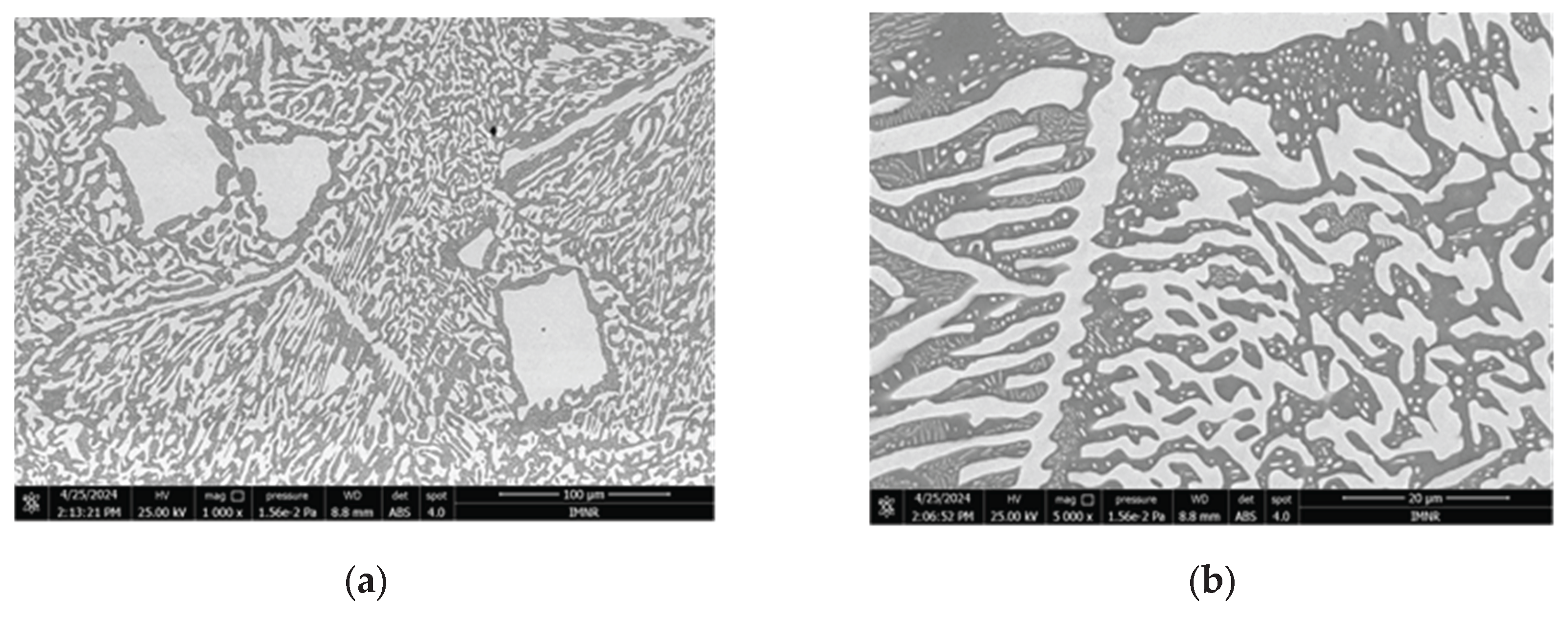
Figure 5.
EDS spectrum of the Bi60Sn40 solder alloy, showing characteristic peaks of bismuth (Bi) and tin (Sn), confirming the binary composition in the analyzed region.
Figure 5.
EDS spectrum of the Bi60Sn40 solder alloy, showing characteristic peaks of bismuth (Bi) and tin (Sn), confirming the binary composition in the analyzed region.
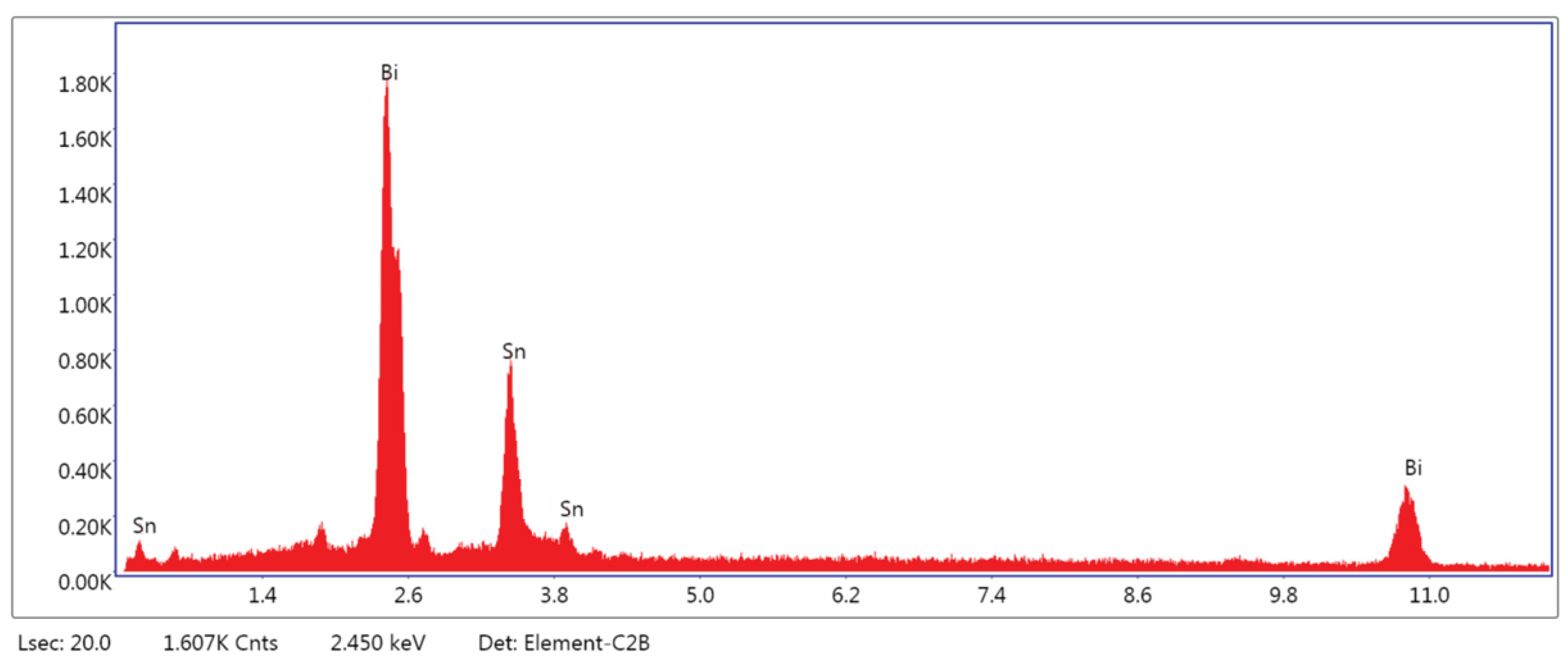
Figure 6.
BSE and elemental mapping images of the Bi60Sn40 solder alloy: (a) BSE micrograph; (b) combined elemental map (Sn – yellow, Bi – red); (c) Sn distribution (65%); (d) Bi distribution (35%). The microstructure reveals a Sn-rich matrix with dispersed Bi-rich regions.
Figure 6.
BSE and elemental mapping images of the Bi60Sn40 solder alloy: (a) BSE micrograph; (b) combined elemental map (Sn – yellow, Bi – red); (c) Sn distribution (65%); (d) Bi distribution (35%). The microstructure reveals a Sn-rich matrix with dispersed Bi-rich regions.
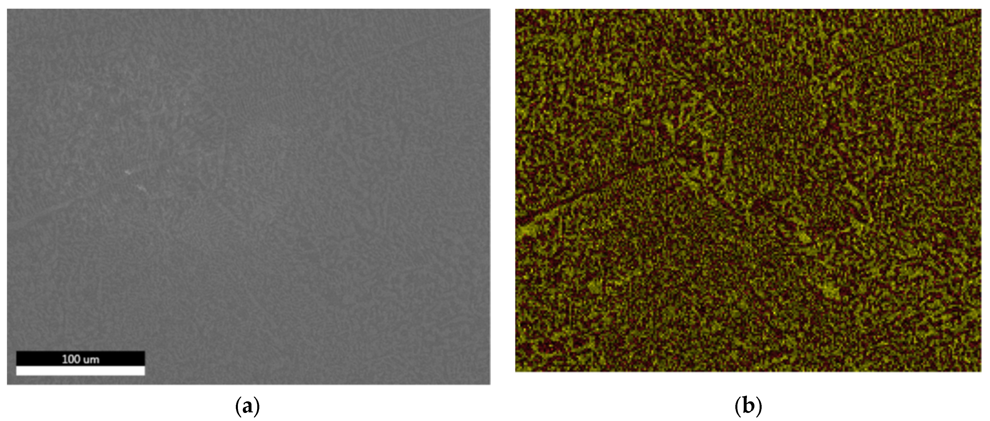
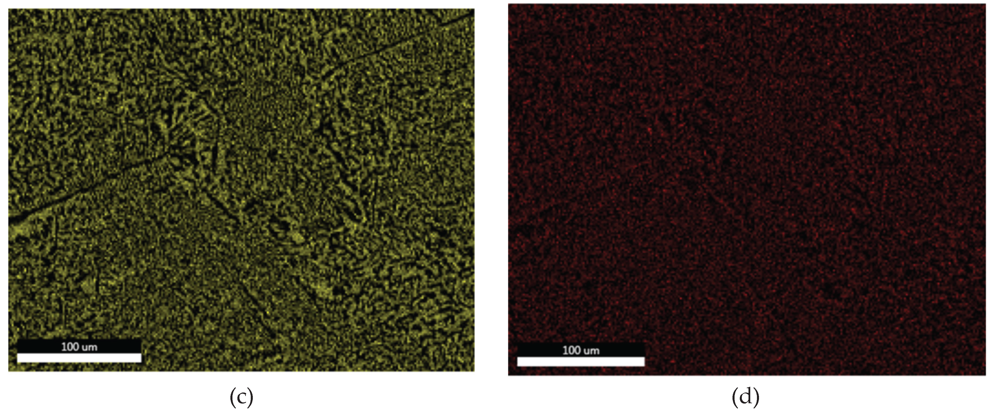
Figure 7.
SEM micrographs of the Bi60Sn35Sb5 alloy: (a) Microstructure with large primary Bi-rich grains embedded in a Sn-rich eutectic matrix and dispersed Sb-containing precipitates (magnification: 1000x); (b) Enlarged view of a primary Bi grain containing a central Sb-rich inclusion and surrounding fine intermetallic dispersions (magnification: 5000x).
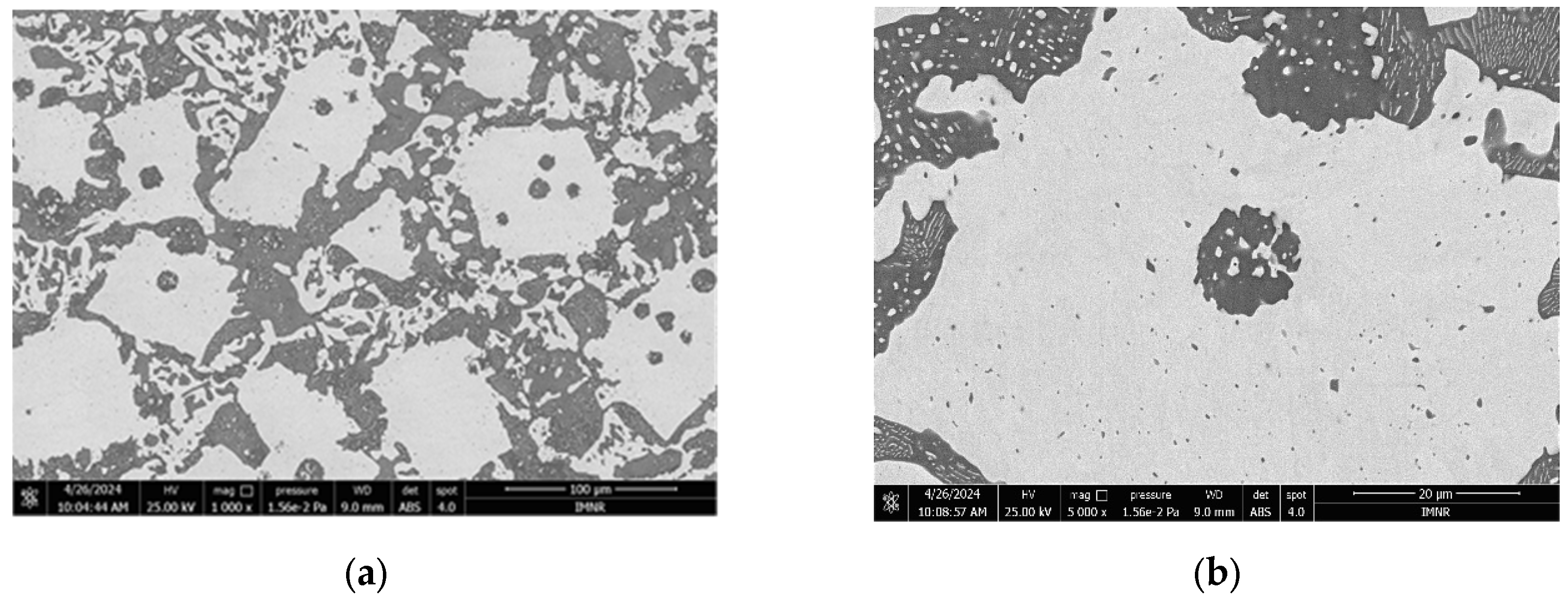
Figure 8.
EDS spectrum of the Bi60Sn35Sb5 solder alloy, indicating the presence of bismuth (Bi), tin (Sn), and antimony (Sb) in the analyzed region.
Figure 8.
EDS spectrum of the Bi60Sn35Sb5 solder alloy, indicating the presence of bismuth (Bi), tin (Sn), and antimony (Sb) in the analyzed region.
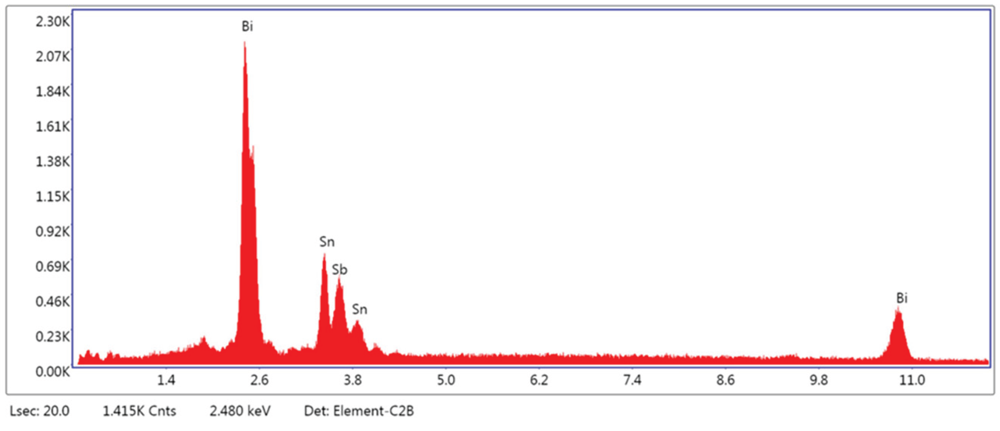
Figure 9.
BSE and elemental mapping images of the Bi60Sn35Sb5 solder alloy: (a) BSE micrograph; (b) combined elemental map (Sn – yellow, Bi – red, Sb – green); (c) Sn distribution (41%); (d) Bi distribution (34%); (e) Sb distribution (22%). The microstructure shows clear phase separation with Sn-rich, Bi-rich, and Sb-containing regions.
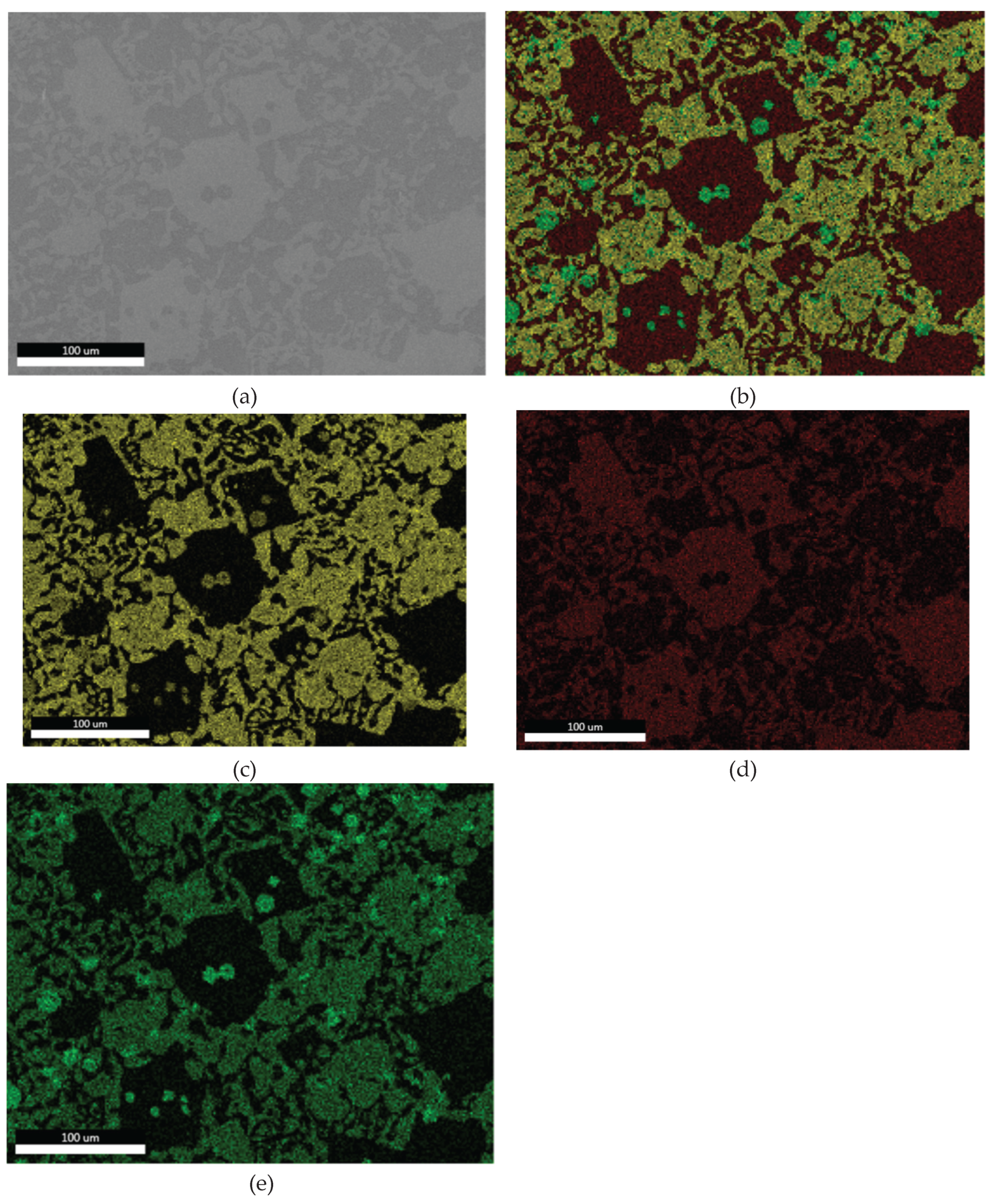
Figure 10.
SEM micrographs of the Bi60Sn35Ag5 solder alloy: (a) General microstructure showing Bi–Sn eutectic regions and elongated intermetallic compounds (magnification: 1000x); (b) Higher magnification image highlighting needle-like Ag3Sn intermetallic phases embedded in the eutectic matrix (magnification: 5000x).
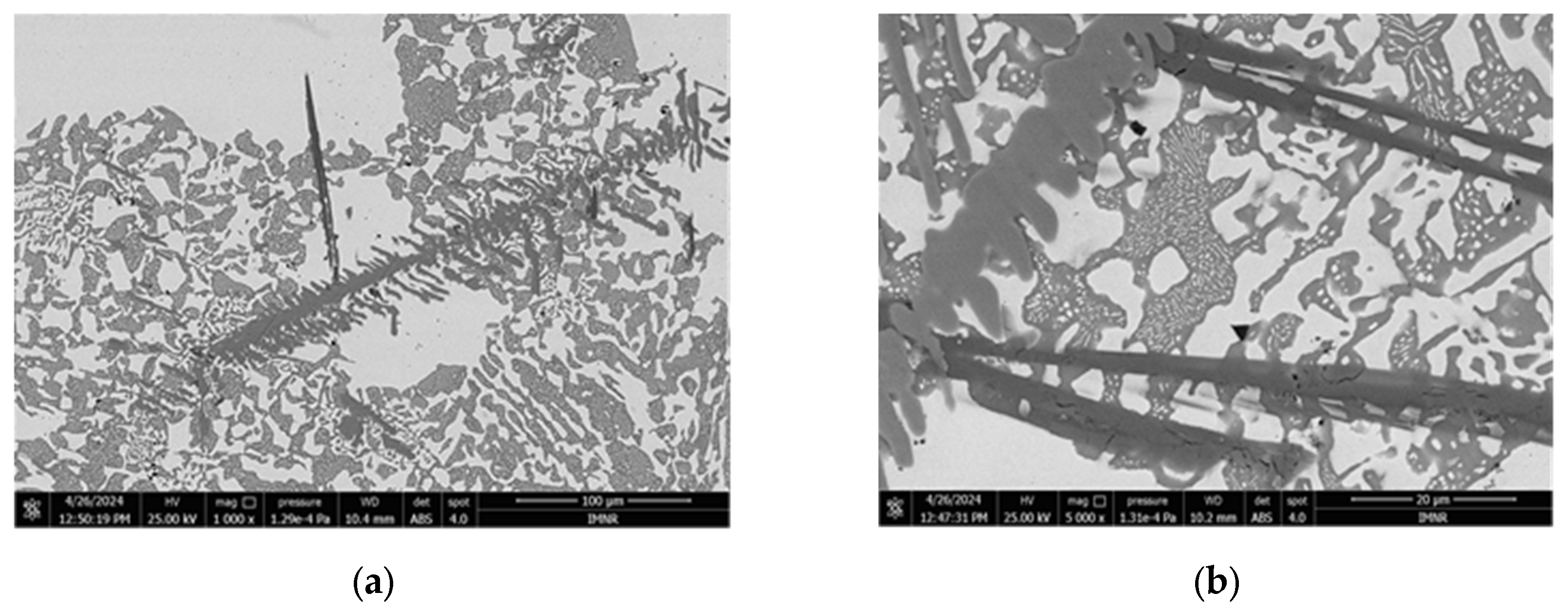
Figure 11.
EDS spectrum of the Bi₆₀Sn₃₅Ag₅ solder alloy showing characteristic peaks of Sn, Ag, and Bi, confirming the presence and approximate proportion of the alloying elements within the analyzed microstructural region.
Figure 11.
EDS spectrum of the Bi₆₀Sn₃₅Ag₅ solder alloy showing characteristic peaks of Sn, Ag, and Bi, confirming the presence and approximate proportion of the alloying elements within the analyzed microstructural region.
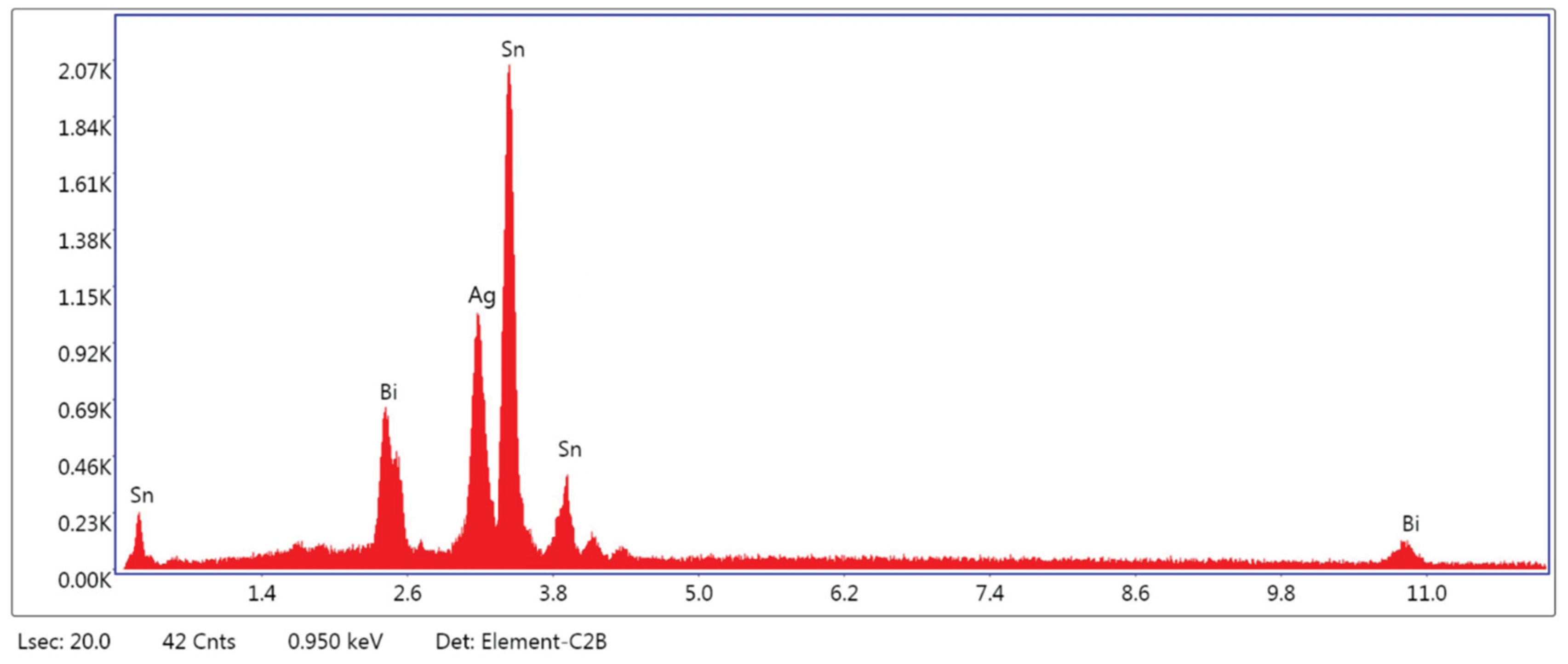
Figure 12.
BSE image and EDS elemental mapping of the Bi60Sn35Ag5 alloy: (a) BSE micrograph; (b) combined EDS map showing Sn (yellow), Bi (red), and Ag (blue); (c) Sn distribution (65%); (d) Bi distribution (35%); (e) Ag distribution (22%). Ag-rich acicular structures are visible along the phase boundaries.
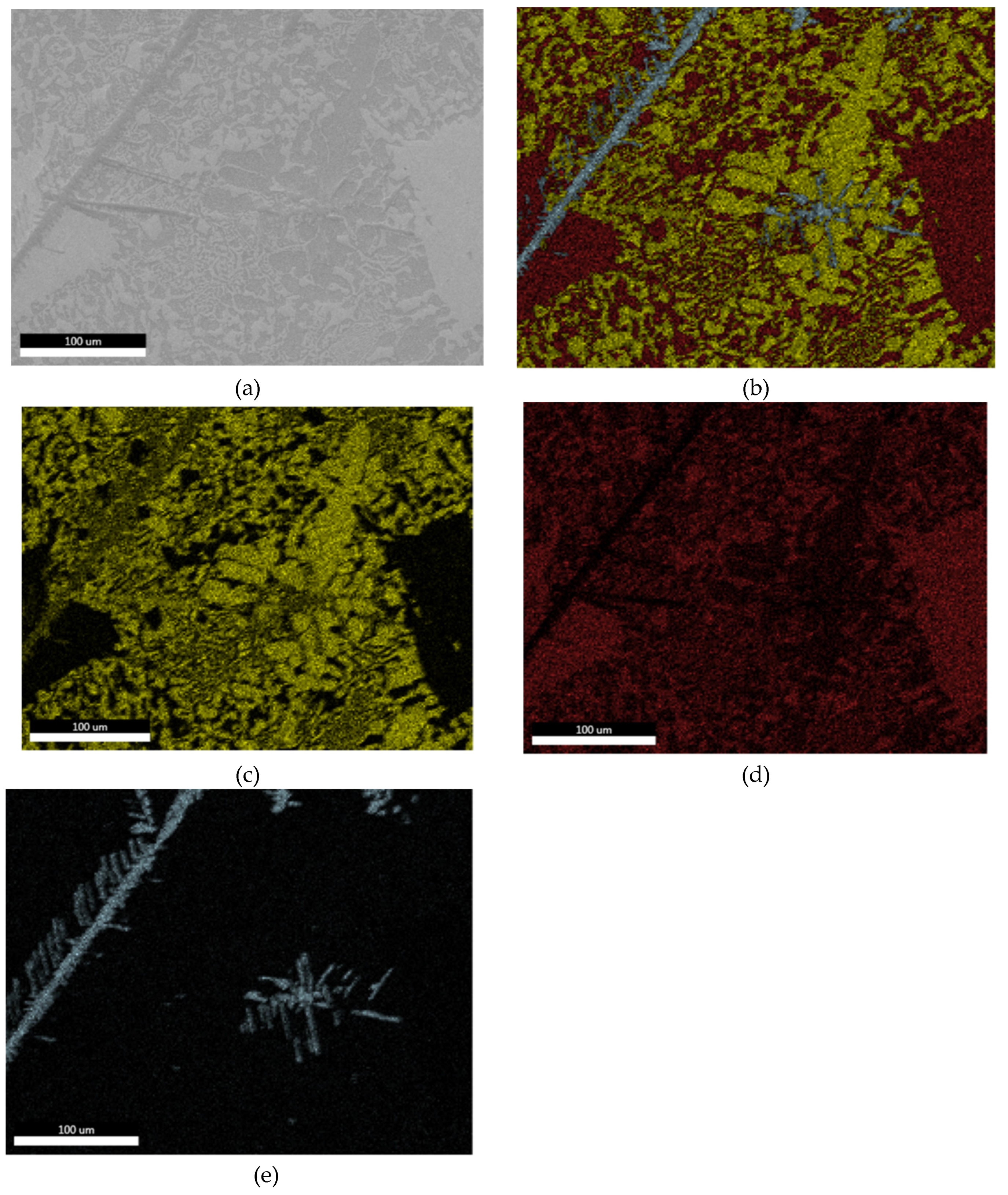

Table 1.
Chemical composition of the Bi-Sn Based Solder Alloys.
| Chemical Composition (%) | |||
|---|---|---|---|
| Element | Bi60Sn40 | Bi60Sn35Sb5 | Bi60Sn35Ag5 |
| Bi | 59.437 | 59.411 | 58.804 |
| Sn | 39.475 | 34.533 | 34.271 |
| Sb | 0.0167 | 4.88 | 0.0177 |
| Ag | 0 | 0 | 4.93 |
| Cu | 0.122 | 0.182 | 1.63 |
| Fe | 0.018 | 0.029 | 0.024 |
| A.E.* | Bal. | Bal. | Bal. |
| Total | 100 | 100 | 100 |
* A.E. – other elements (Al, C, Pb, Si, Zr, Zn).
Table 2.
Elemental composition of the Bi60Sn40 solder alloy determined by EDS analysis.
| Analysis | Element | Weight % | Atomic % | Net Int. | Error % | P/B Ratio | R | F |
| EDS | SnL | 31.51 | 44.75 | 411.53 | 7.86 | 167.6377 | 1.0575 | 1.0067 |
| BiL | 68.49 | 55.25 | 280.07 | 12.92 | 182.9532 | 1.1144 | 1.0457 | |
| Total | 100.00 | 100.00 |
Table 3.
Elemental composition of the Bi60Sn35Sb5 solder alloy determined by EDS analysis.
| Analysis | Element | Weight % | Atomic % | Net Int. | Error % | P/B Ratio | R | F |
| EDS | SnL | 20.20 | 29.05 | 371.86 | 8.01 | 101.1552 | 1.0578 | 1.0071 |
| SbL | 9.87 | 13.84 | 185.19 | 11.58 | 49.3374 | 1.0601 | 1.0073 | |
| BiL | 69.93 | 57.12 | 351.90 | 13.20 | 175.2969 | 1.1150 | 1.0456 | |
| Total | 100.00 | 100.00 |
Table 4.
Elemental composition of the Bi60Sn35Ag5 solder alloy determined by EDS analysis.
| Analysis | Element | Weight % | Atomic % | Net Int. | Error % | P/B Ratio | R | F |
| EDS | SnL | 68.09 | 71.90 | 1394.17 | 6.89 | 329.1566 | 1.0388 | 1.0063 |
| AgL | 25.82 | 24.78 | 340.73 | 9.98 | 121.4951 | 1.0443 | 1.0038 | |
| BiL | 6.09 | 3.32 | 11.19 | 63.37 | 16.6575 | 1.0880 | 1.0600 | |
| Total | 100.00 | 100.00 |
Table 5.
Thermal and electrical conductivity data of the solder alloys between 25°C and 140°C.
| Solder alloy | Temp. (°C) | α (m²/s) | λ (W/m·K) | ρ (Ω·m) | σ (S/m) |
|---|---|---|---|---|---|
| Bi60Sn40 | 25 | 10.75·10-6 | 16.9316 | 3.80·10⁻⁷ | 2.63·10⁶ |
| 50 | 11.85·10-6 | 18.9363 | 4.45·10⁻⁷ | 2.25·10⁶ | |
| 75 | 12.90·10-6 | 20.9289 | 5.10·10⁻⁷ | 1.96·10⁶ | |
| 100 | 13.93·10-6 | 22.9343 | 6.35·10⁻⁷ | 1.57·10⁶ | |
| 125 | 14.93·10-6 | 24.9331 | 7.60·10⁻⁷ | 1.32·10⁶ | |
| 140 | 16.06·10-6 | 26.9261 | 8.35·10⁻⁷ | 1.20·10⁶ | |
| Bi60Sn35Ag5 | 25 | 11.91·10-6 | 18.2788 | 1.52·10⁻⁷ | 6.54·10⁶ |
| 50 | 11.56·10-6 | 18.2486 | 1.66·10⁻⁷ | 6.15·10⁶ | |
| 75 | 10.80·10-6 | 17.5224 | 1.77·10⁻⁷ | 5.69·10⁶ | |
| 100 | 10.46·10-6 | 17.4294 | 1.89·10⁻⁷ | 5.33·10⁶ | |
| 125 | 9.89·10-6 | 16.9133 | 2.01·10⁻⁷ | 4.98·10⁶ | |
| 140 | 9.56·10-6 | 16.7682 | 2.08·10⁻⁷ | 4.81·10⁶ | |
| Bi60Sn35Sb5 | 25 | 9.71·10-6 | 13.8968 | 1.53·10⁻⁷ | 6.52·10⁶ |
| 50 | 9.11·10-6 | 13.5846 | 1.63·10⁻⁷ | 6.12·10⁶ | |
| 75 | 8.66·10-6 | 13.4331 | 1.76·10⁻⁷ | 5.67·10⁶ | |
| 100 | 7.23·10-6 | 11.6486 | 1.88·10⁻⁷ | 5.30·10⁶ | |
| 125 | 6.81·10-6 | 11.3805 | 2.00·10⁻⁷ | 4.86·10⁶ | |
| 140 | 6.22·10-6 | 10.6610 | 2.08·10⁻⁷ | 4.79·10⁶ |
Disclaimer/Publisher’s Note: The statements, opinions and data contained in all publications are solely those of the individual author(s) and contributor(s) and not of MDPI and/or the editor(s). MDPI and/or the editor(s) disclaim responsibility for any injury to people or property resulting from any ideas, methods, instructions or products referred to in the content. |
© 2025 by the authors. Licensee MDPI, Basel, Switzerland. This article is an open access article distributed under the terms and conditions of the Creative Commons Attribution (CC BY) license (http://creativecommons.org/licenses/by/4.0/).
Copyright: This open access article is published under a Creative Commons CC BY 4.0 license, which permit the free download, distribution, and reuse, provided that the author and preprint are cited in any reuse.


