
Submitted:
07 May 2025
Posted:
13 May 2025
You are already at the latest version
Abstract
In many modern power electronic systems, accurate modeling is critical for effective control design and overall system performance. This paper examines the derivation of AC equivalent circuit models for pulse‐width modulated (PWM) converters operating in the continuous conduction mode. The primary goal is to isolate the significant low‐frequency behavior of converters by removing the high‐frequency switching components inherent to their operation. To accomplish this, the paper outlines both state‐space averaging and circuit averaging techniques, emphasizing how inductor currents and capacitor voltages can be approximated by averaged quantities over one switching period. Derivations are presented for key topologies—including buck, boost, and buck‐boost converters—to demonstrate the process of constructing small‐signal transfer functions. Practical considerations such as conduction losses, diode drops, and on‐resistance effects are also integrated to reflect real‐world conditions. By capturing the essential dynamics in a linearized form, these averaged models enable standard analytical tools (such as Bode plot analysis) to guide controller design, stability assessments, and transient response optimizations. Concluding remarks highlight the versatility of these methods and recommend directions for future exploration, including extensions to discontinuous conduction and resonant modes. The results underscore the value of averaged modeling as a foundation for robust and efficient power converter design.
Keywords:
AC equivalent circuit modeling
; State‐space averaging
; circuit averaging
; averaged switch model
; canonical circuit
; Small‐signal analysis
; DC‐DC converters
; Power electronics
1. Introduction and Background
Switch-mode power converters are widely used in modern electronics, providing efficient methods for transferring and regulating power in applications that range from small portable devices to large-scale industrial systems. By rapidly switching transistors between fully on and fully off states, these converters minimize dissipation and achieve high operating efficiency. However, the rapid transitions intrinsic to the switching action also generate high-frequency components in current and voltage waveforms, making direct analysis cumbersome when focusing on low-frequency behavior or feedback loop design.
In many practical situations, especially where precise output regulation is required, engineers are far more interested in the slower dynamics that govern steady-state accuracy and transient response than in the switching harmonics themselves. For example, in a basic step-down (buck) converter, the inductor current ripples rapidly each cycle, but the gradual changes in its average value have the most significant effect on output regulation and system stability. The ripple can be sufficiently small that its influence on feedback design is negligible, prompting the use of modeling techniques that average out the switching action over a single period.
Figure 1.
Typical DC–DC Buck Converter with Voltage Feedback Loop.

Two closely related methods—state-space averaging and circuit averaging—have proven particularly valuable for modeling switch-mode converters in the continuous conduction mode. Both involve identifying how inductor voltages and capacitor currents change when a transistor or diode toggles between conduction and non-conduction intervals, then representing these time-varying connections with averaged expressions. In state-space averaging, one writes linear differential equations valid during each subinterval of the switching period, combines them according to duty ratio, and obtains a piecewise-averaged system that captures the low-frequency behavior. In circuit averaging, the focus shifts to replacing the active switches with equivalent dependent sources or averaged switch networks, ultimately forming a time-invariant circuit suitable for analysis with standard linear techniques.
These modeling strategies are essential for designing robust feedback loops. Without an adequate small-signal representation, it is difficult to predict how a converter will respond to a sudden load change, a variation in input voltage, or an alteration in reference commands. Averaged models, once linearized about a chosen operating point, yield transfer functions (for instance, control-to-output or line-to-output) that can be evaluated using traditional frequency-domain tools. This allows designers to set bandwidth, phase margin, and other specifications that ensure stability and satisfactory transient performance.
Furthermore, while the basic principles are usually illustrated by low-power, single-phase examples such as buck, boost, and buck-boost converters, the same techniques extend to more complex configurations. Transformer-based topologies and multi-phase converters can be treated similarly, albeit with additional care in accounting for winding ratios, parasitic elements, and conduction modes. In all cases, the strength of the averaged modeling approach lies in striking a practical balance between simplicity and accuracy. The use of averaged models drastically reduces the mathematical complexity of high-frequency switching phenomena while retaining enough detail to make meaningful predictions about the converter’s behavior under typical operating conditions.
In the chapters and sections that follow, a step-by-step approach is taken to show how these models are derived and validated. This includes handling the principal energy-storage elements, incorporating conduction losses or voltage drops as needed, and performing the small-signal linearization that underpins frequency-response analysis. By illustrating these ideas through multiple converter topologies, the paper highlights the versatility of averaged modeling as a unifying framework for continuous conduction designs. In doing so, it provides a foundation for understanding the essential dynamics behind switch-mode power conversion and for designing controllers that meet demanding performance requirements.
2. Fundamentals of Averaged Modeling
Averaged modeling is a powerful approach for analyzing switch-mode power converters without tracking every transition of the high-speed switching elements. In many practical designs, inductors and capacitors are chosen so that the switching ripple in their currents or voltages remains modest, allowing one to approximate these signals by their average values over a single switching period. This simplification makes it possible to study the converter’s low-frequency or system-level behavior in a more straightforward way, which is particularly useful for control design and stability analysis.
Figure 2.
Buck Converter Inductor and Capacitor Waveforms, Including Their Averages Over One Switching Period.
Figure 2.
Buck Converter Inductor and Capacitor Waveforms, Including Their Averages Over One Switching Period.
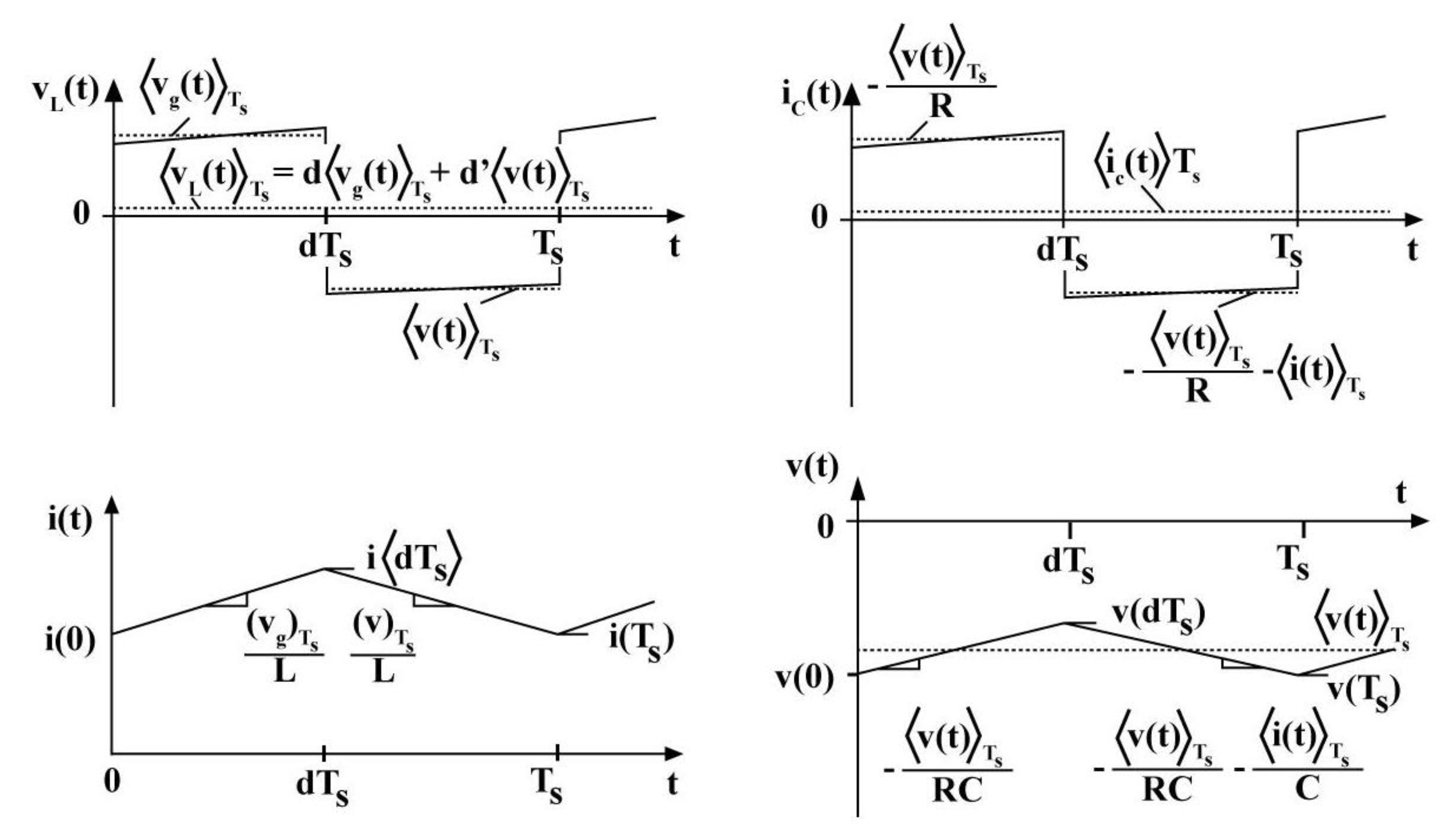
A convenient starting point is to focus on one inductor and one capacitor, recognizing that many converters can be broken down into a small set of these energy-storage components. Consider an inductor of value subjected to two different voltage levels, and , within each switching period . For a fraction of the period, the inductor experiences (such as when a transistor is on), and for the remaining , it experiences (such as when a diode is conducting). The instantaneous inductor voltage, , follows a piecewise function, but can be replaced by its average over :
where is the duty cycle. This same principle applies to capacitors by averaging their current waveform over . In that case, if flows into the capacitor for a fraction and flows in for , the average capacitor current is
Such expressions rely on two main assumptions. First, the inductor current and capacitor voltage should not change drastically within each subinterval of length or . This is often referred to as the small-ripple approximation, indicating that the actual waveforms do not deviate significantly from their average during one switching period. Second, the overall time constants of the converter’s energy-storage elements (dominated by and ) must be much larger than , ensuring that the averaged representation remains valid for frequencies well below the switching frequency .

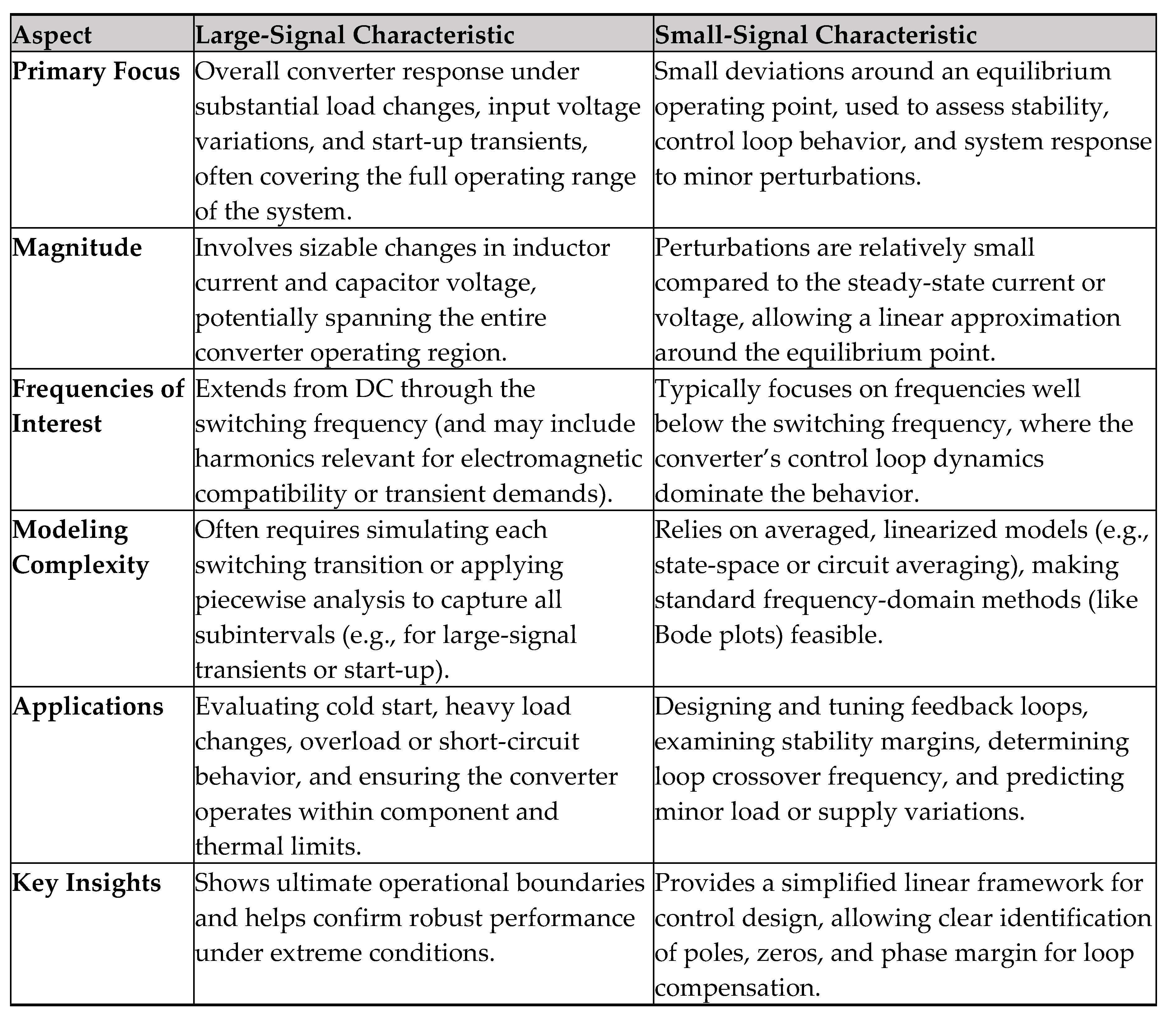
Table 1.
Comparison of Large-Signal vs. Small-Signal Characteristics.
 |
In practice, there are two closely related ways to create these averaged models. One is known as state-space averaging, which involves writing down differential equations for each subinterval and taking a weighted average based on . Another approach, circuit averaging, treats the switch network (usually composed of a transistor and a diode) as a two-port element that can be replaced by controlled sources or an equivalent “transformer” in the time-invariant version of the converter schematic. Despite these different viewpoints, both methods ultimately yield a set of equations that describe how the average inductor current and capacitor voltage evolve over time.
When averaged models are applied under steady-state conditions, two key relationships often emerge. The first is inductor volt-second balance, which states that the inductor’s average voltage over one switching period must be zero if its current is to remain constant from cycle to cycle. Symbolically,
in a hypothetical two-level system (with the sign depending on specific circuit polarity). The second is capacitor charge balance, indicating that the net charge flowing into the capacitor over one cycle must be zero for the capacitor voltage to remain stable:
These balance conditions provide a convenient way to calculate the converter’s equilibrium operating point (such as output voltage and inductor current) without delving into the switching ripple details.
Following the derivation of average voltages and currents, designers often take one more step: linearizing the averaged equations around a chosen operating point to obtain a small-signal model. This model helps predict how the converter responds to small perturbations, such as changes in load, input voltage, or duty cycle commands. In linearized form, well-known frequency-domain tools like Bode plots and Nyquist diagrams become applicable, enabling the design of feedback loops that meet bandwidth and stability requirements.
In summary, averaged modeling provides a practical balance between the complexity of time-domain switching waveforms and the need to understand a converter’s essential dynamics at lower frequencies. By replacing piecewise voltages and currents with their cycle averages, one arrives at a continuous-time representation that is more amenable to classical control analysis. This framework forms the backbone of the small-signal design process for many switch-mode power converters.
3. State-Space Averaging Method
The state-space averaging method provides a structured approach to modeling the low-frequency dynamics of switching converters. By writing the converter inductor currents and capacitor voltages in the form of state variables and then defining corresponding linear equations for each interval of the switching cycle, one can systematically derive an averaged model that offers clear insight into system-level behavior.
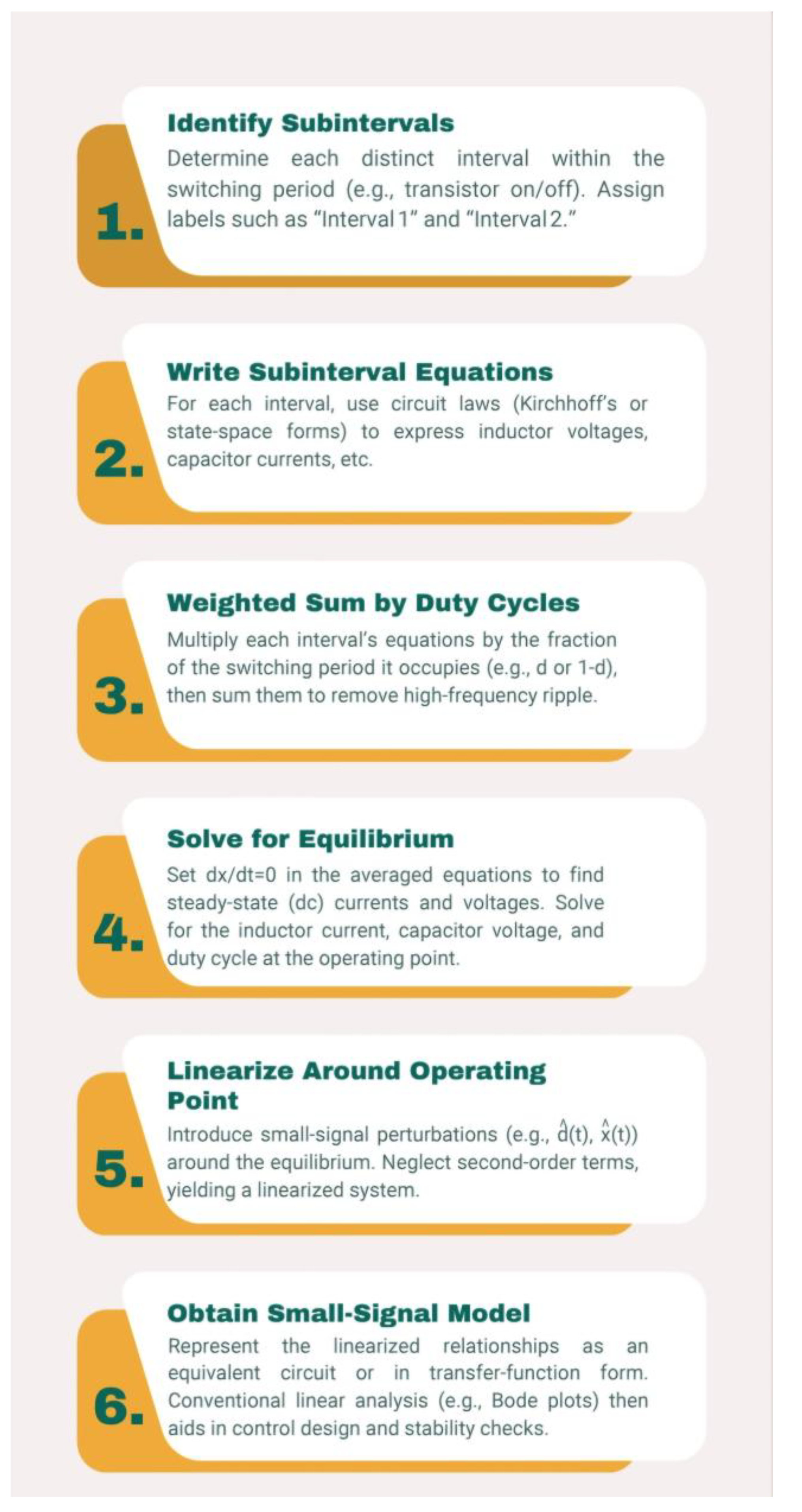
Figure 3.
Flow Diagram for Subinterval Equations, Averaging, and Linearization.
- Purpose and Basic Concept
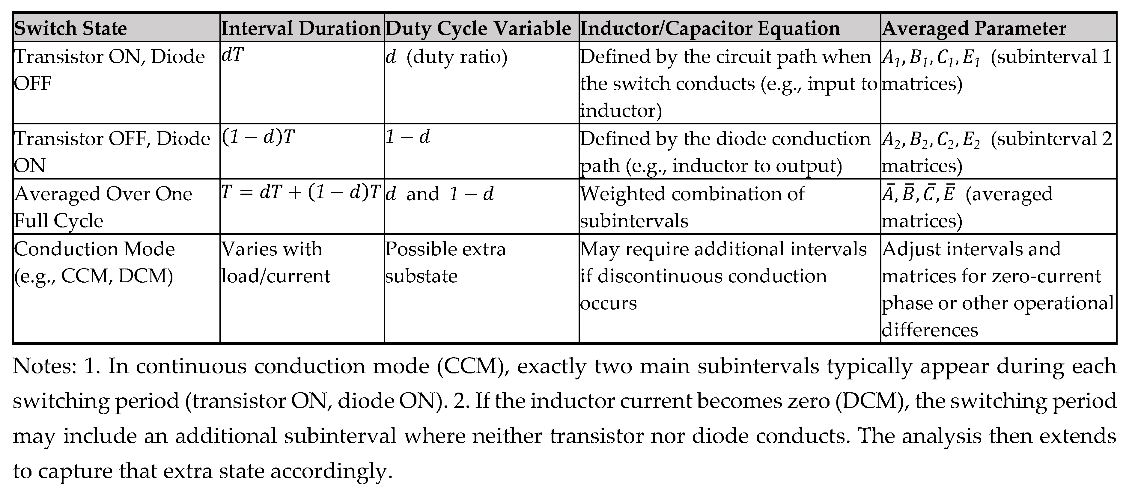
Switch-mode converters typically operate in two (or more) distinct topologies over the course of each switching cycle: for example, a transistor-on interval (subinterval 1) and a transistor-off interval (subinterval 2). In each subinterval, the circuit can be described by linear differential equations involving the inductor and capacitor variables. The key idea of state-space averaging is to write these equations in a standard matrix form, then combine them by weighting with the fraction of time spent in each subinterval (i.e., the duty cycle). By applying this procedure, one obtains a single time-invariant system that represents the converter’s behavior at frequencies much lower than the switching frequency.
- 2.
- State Equations for Subintervals
In continuous conduction mode (CCM), a common approach is to identify:
- The state vector , consisting of independent inductor currents and capacitor voltages.
- The input vector , which includes sources such as the input voltage and any relevant control signals.
- The output vector , which contains dependent quantities like the converter’s output current or input current.
Table 2.
Summary of State-Space Model Notation.
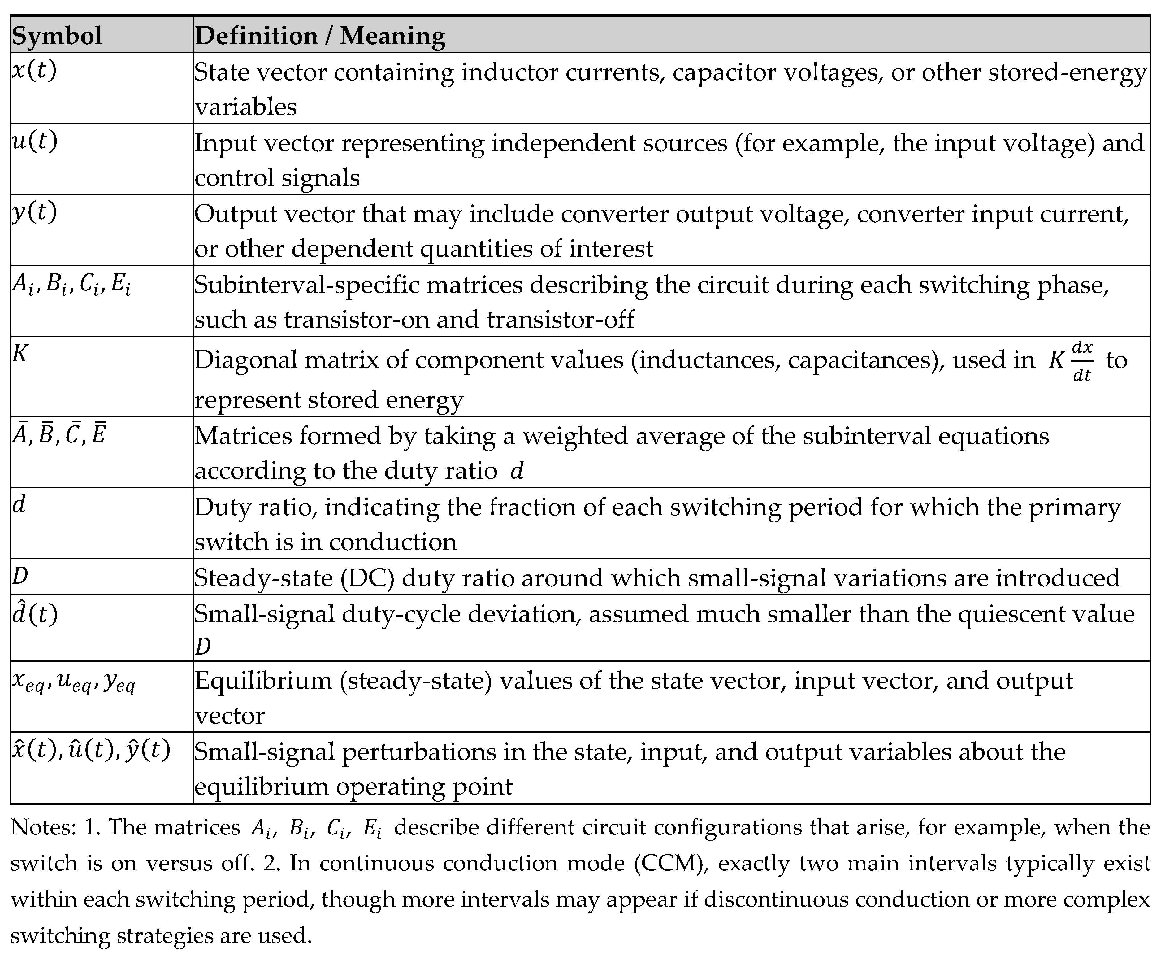 |
For a two-subinterval PWM converter, one writes the following generic linear equations for each subinterval :
Here, is typically a diagonal matrix of inductances and capacitances, while , , , and reflect how the circuit is connected during interval . For instance, when the main switch is on, the transistor and diode may form one topology; when it is off, the diode and output filter may form another. The switching period is divided into two portions: interval 1 of length and interval 2 of length .
- 3.
- Averaging Over the Switching Period
To capture the low-frequency evolution of the state variables without tracking every switching transition, one defines an averaged state vector and similarly averaged input and output . Under the assumption that and do not change significantly within a single cycle (the small-ripple approximation), the converter’s behavior can be approximated by:
This equation, often referred to as the averaged state-space equation, applies for frequencies much less than the switching frequency. By distributing and , one can identify the matrices:
leading to
A similar relation governs the averaged output , yielding:
where
- 4.
- Equilibrium (Steady-State) Solution
For many practical applications, an important first step is to determine how the converter operates at steady state. In this situation, the derivatives of the averaged state variables are zero, so:
By solving this matrix equation, one finds the equilibrium inductor current and capacitor voltage (and other relevant internal variables). These equilibrium values are used later as a reference point for small-signal linearization. A well-known example is the buck converter, where the averaged approach reveals the familiar relationship under idealized conditions.
Once the steady-state (or quiescent) solution , is known, the next step is to analyze small deviations around that point. Let
where the hat symbol denotes a small perturbation. Substituting these into the averaged equations and retaining only first-order terms (i.e., neglecting products of small signals) yields a linear system describing how and evolve with time. Symbolically, one can express this as:
where and arise from the dependence of , , , on . The term captures the direct effect of duty-cycle perturbations on the state variables. A parallel set of equations defines the perturbed output .
- 6.
- Example Highlights
A common illustration is the buck-boost converter, which has a single inductor and a single capacitor. One writes , then defines subinterval-1 matrices , , , based on how the inductor and capacitor are connected when the transistor is on, and subinterval-2 matrices , , , for when the transistor is off. After forming the averaged matrices , , , , the user can solve for the equilibrium operating point. Perturbing around that point makes it possible to obtain transfer functions such as (control-to-output), which is essential for determining the converter’s frequency response and designing a compensation network.
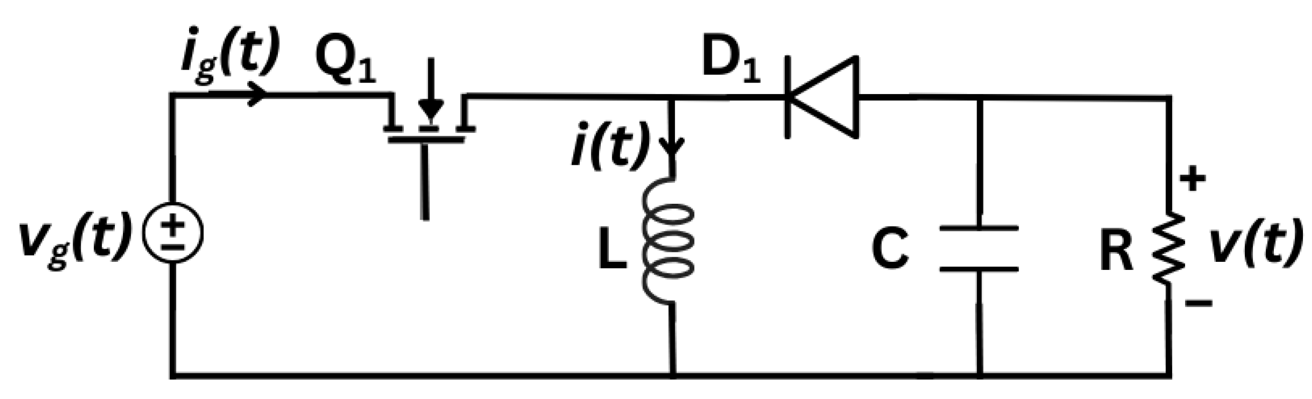
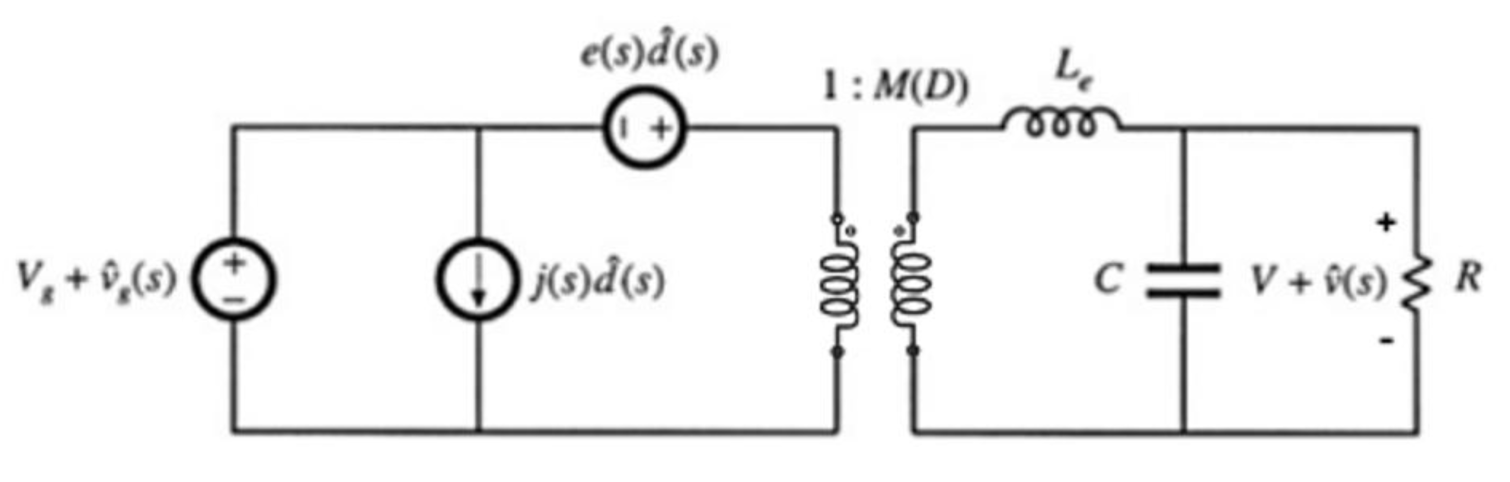
Figure 4.
Nonideal Buck-Boost Converter Schematic with MOSFET On-Resistance and Diode Drop.
- 7.
- Advantages and Practical Considerations
The state-space averaging method excels in providing a clear, unified representation of how the converter evolves over each switching cycle. Because the final averaged equations no longer explicitly depend on time-varying connections, analysis becomes much more tractable. In addition, the resulting framework is naturally compatible with well-established control-system techniques.
One should be aware, however, that this approach relies on the assumption that the converter stays in continuous conduction mode and experiences relatively small ripple in its state variables over each cycle. If the inductor current or capacitor voltage undergoes large swings within the switching period, a more detailed analysis may be warranted. Moreover, in modes such as discontinuous conduction or when current programming is employed, the standard two-subinterval state-space averaging may need modifications or additional subintervals.
In conclusion, state-space averaging distills the essential behavior of a switching converter into a simpler time-invariant system valid at frequencies well below the switching rate. This technique offers a direct path to computing steady-state conditions, deriving small-signal transfer functions, and ultimately designing robust controllers that meet performance goals for regulation and transient response.
4. Circuit Averaging and the Averaged Switch Model
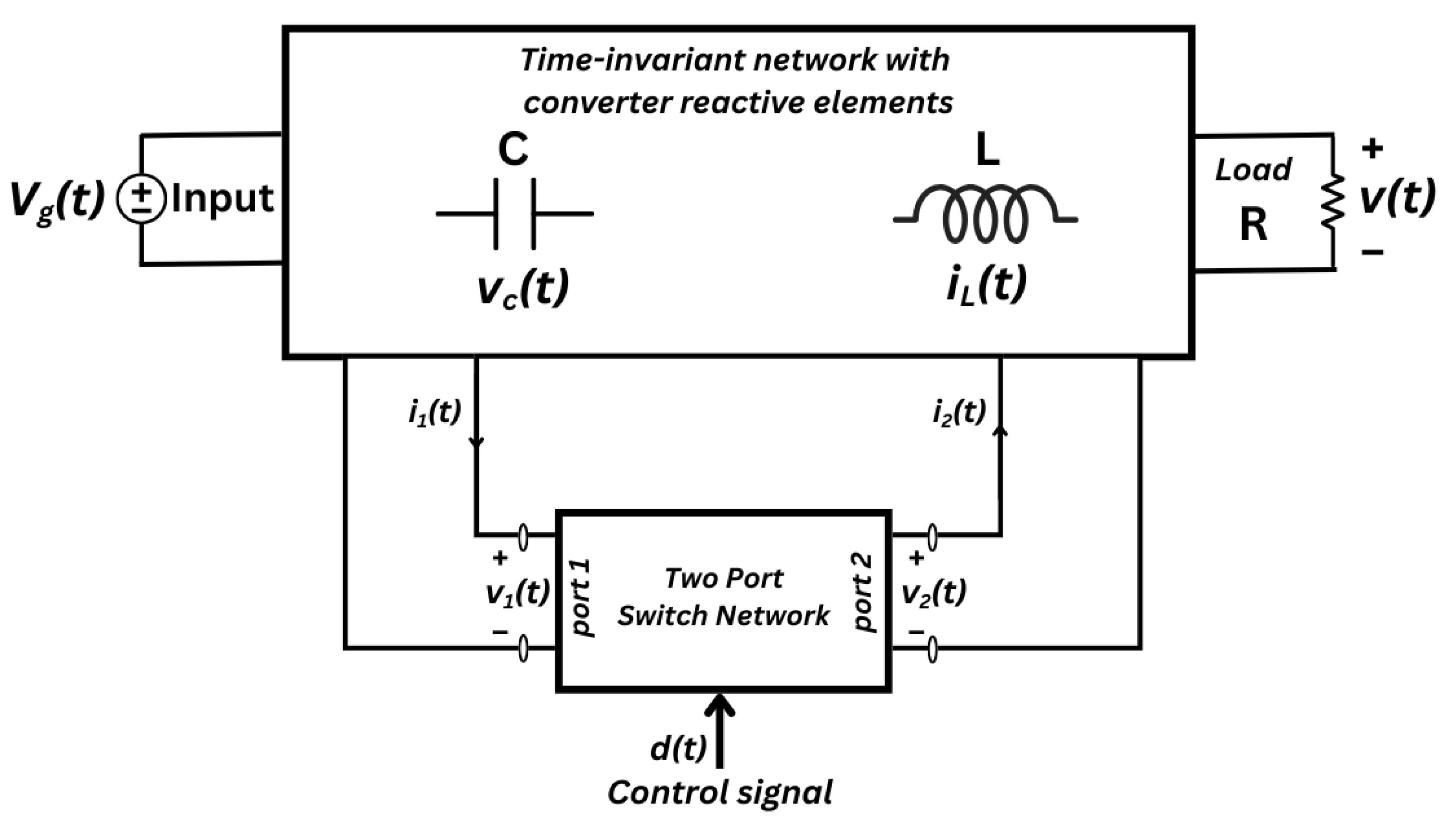
Circuit averaging is a valuable approach for analyzing the behavior of switching converters without having to track each rapid on-off transition of the power devices. Instead of writing separate differential equations for each subinterval of the switching cycle (as in state-space averaging), one identifies the switching elements—usually a transistor and diode network—as a set of ports. The rest of the converter (inductors, capacitors, load, and input source) remains in place. By “averaging out” the time-varying connections of the switch network, the converter can be viewed as a single, time-invariant circuit.
Figure 5.
Generic Two-Port Switch Network with Labeled Terminals.
- Rationale and Basic Idea
When a transistor and diode alternate between conducting and non-conducting states at high frequency, they effectively force the inductor and capacitor into different circuit configurations within a single switching period. The goal of circuit averaging is to combine these configurations into a single equivalent circuit that captures the converter’s net effect on low-frequency signals. To accomplish this, the key step is to replace the actual transistor-diode arrangement with a simplified two-port device whose voltages and currents are “averaged” over the switching period.
As an illustration, consider a basic boost converter. The inductor and load remain fixed, but the transistor and diode switch in such a way that the inductor is connected to the input source when the transistor conducts and to the output node when the diode conducts. Circuit averaging lumps these two subintervals together, forming a single model of the switch network. One can then combine the averaged switch network with the inductor, capacitor, input, and load to produce a time-invariant representation.
- 2.
- Defining the Ports and Averaging
In a typical two-port switch network, each port has a voltage-current pair. Suppose port 1 is and port 2 is . Over one switching period , these variables may exhibit pulsed waveforms. Denote the duty cycle by , so the first subinterval spans and the second spans . If one measures, for example, when the transistor is on and off, it generally takes one value for a fraction and another for . By integrating or summing these values over the entire period, one defines an average voltage:
Similar expressions hold for . The essence of circuit averaging is to identify relationships among these averaged voltages and currents. In many continuous conduction mode (CCM) converters, these relationships take a form akin to
where the extra source terms might represent diode drops or other parasitic effects.
Table 3.
Mapping of Converter Switch States to Averaged Model Parameters.
 |
- 3.
- The Averaged Switch Model
Once the average port variables are identified, it is often helpful to redraw the converter with the switch network replaced by an averaged model. A common representation involves an ideal transformer with a “turns ratio” set by the duty cycle. For instance, if one port’s voltage is and the other’s is , and they relate by in an idealized scenario, then one can depict a transformer that scales voltages by . In parallel, controlled sources may appear in the circuit to inject or draw current in proportion to the duty cycle.
Figure 6.
Averaged Switch Model with Ideal Transformer and Dependent Sources.
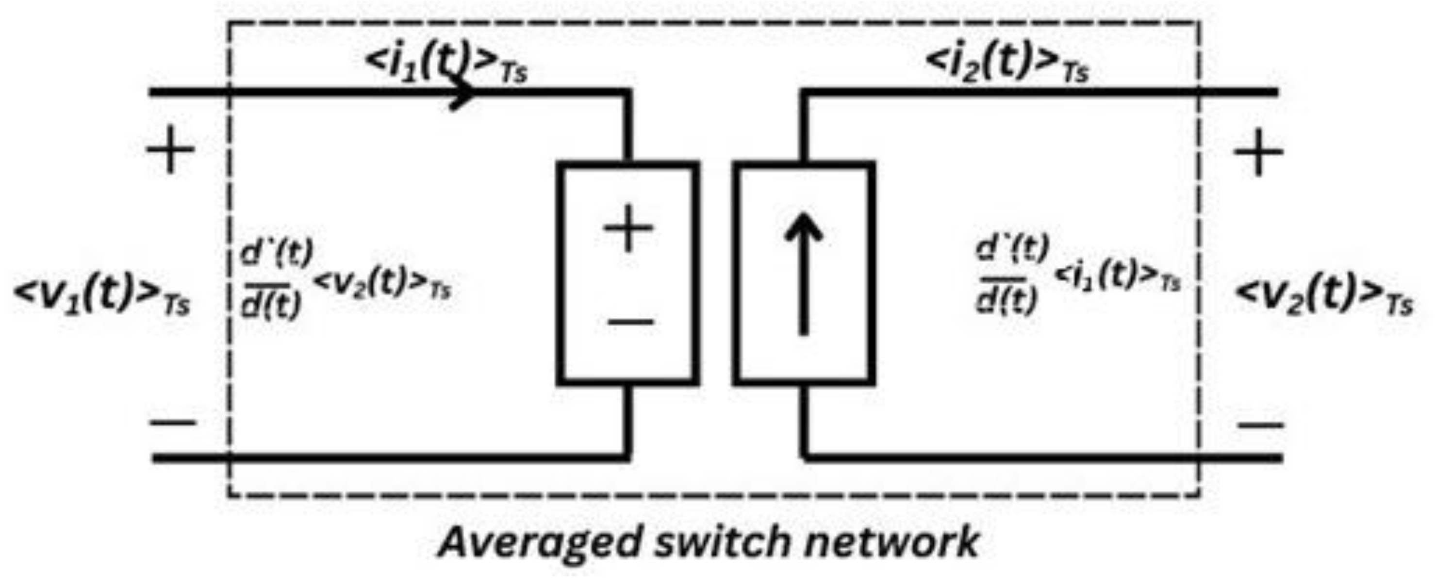
For a boost converter, an averaged switch model might show that the average current entering from the inductor side is , while the average voltage seen at the output side is scaled by , depending on how the two ports are defined. Each converter topology has its own characteristic form of these relationships.
- 4.
- Example: Circuit Averaging in a Buck Converter
Consider a buck converter with a single transistor and a diode. During the “on” phase, the switch connects the input to the inductor, and the diode is reverse-biased. During the “off” phase, the transistor opens, the diode conducts, and the inductor current flows into the load. If we define:
- Port 1 at the transistor input side ,
- Port 2 at the diode output side ,
then one can work out how and behave over a full cycle, and replace the actual switching elements with a voltage source or current source that captures the average effect. For example, if is the average current from the input side, then in CCM, one often finds if is the inductor current, because the transistor effectively connects port 1 to the inductor for a fraction of the time. The net result is a circuit with fewer time-varying branches, where each source or transformer is controlled by , but otherwise remains a static element over the analysis interval.
- 5.
- Including Large-Signal Behavior and Linearization
Like state-space averaging, circuit averaging can be expressed first as a large-signal model. This form indicates how the duty cycle and average inductor or capacitor waveforms interact to determine the converter’s steady-state operating point. One can then linearize around that steady operating point by writing:
and so on. Products of small signals are discarded, leaving first-order terms that define the linear small-signal relationships. Often, these end up implying that each transformer winding in the averaged switch model is accompanied by a dependent source whose value is tied to the steady-state current or voltage multiplied by the duty-cycle perturbation.
- 6.
- Benefits and Practical Considerations
Circuit averaging offers a straightforward way to “see” how duty cycle modulates the flow of energy. By focusing on a two-port (or multi-port) switch network, one can reuse standard circuit analysis tools to find transfer functions, input or output impedances, or the converter’s frequency response. This approach complements state-space averaging, and both methods should yield consistent results if all assumptions—continuous conduction, small ripple, and high switching frequency relative to system bandwidth—are satisfied.
However, large ripple, discontinuous conduction mode, and other complexities may necessitate caution. Additional subintervals or specialized models might be required. Still, for many continuous conduction designs operating at moderate ripple, circuit averaging and the averaged switch model remain dependable techniques. They provide a concise, physically insightful view of how transistors and diodes guide energy from the source to the load on average, ultimately simplifying both analysis and design of controllers for low-frequency dynamics.
In summary, circuit averaging moves beyond time-domain switching details by substituting the actual high-frequency transistor-diode network with averaged voltage and current sources (or transformers plus sources). When combined with the converter’s inductors, capacitors, and resistive elements, this yields a time-invariant model that is well suited to Bode-plot analysis, controller tuning, and system-level optimization.
5. Canonical Model Representation
The idea of a canonical model emerges when examining the small-signal behavior of any continuous-conduction-mode (CCM) converter driven by pulse-width modulation (PWM). Although different converters—buck, boost, buck-boost, forward, flyback, and others—arrange their switches, inductors, and capacitors in various ways, the underlying control actions and energy-transfer processes share fundamental similarities. By isolating those shared dynamics, one can write a standardized set of equations or construct a single “canonical” circuit that models how duty-cycle perturbations affect inductor currents, capacitor voltages, and the converter’s output.
- Motivation for a Canonical Form
In small-signal analyses, each converter’s differential equations can be linearized about an operating point, typically defined by a quiescent duty ratio and steady-state inductor current and capacitor voltage. The resulting expressions often reveal a second-order (or higher) system governed by inductor-capacitor interactions and altered by duty-cycle variations. Since all CCM PWM converters must, in some sense, regulate energy flow from an input source to an output through switching devices, it is possible to group the resulting transfer functions and impedances into a more general form that applies to multiple topologies.
By casting the converter’s inductor(s), capacitor(s), and load into a generic two-port framework, the small-signal model becomes a standardized network. Key features include:
- An ideal transformer-like element associated with the average conversion ratio.
- Dependent sources that introduce duty-cycle control variations into the node and loop equations.
- Inductor and capacitor elements that store and release energy, dictating dynamic behavior.
Figure 7.
Canonical Circuit Model for PWM Converters.
- 2.
- Standardized Small-Signal Equations
A central goal is to represent the control-to-output transfer function, line-to-output transfer function, and output impedance in a way that highlights the roles of the inductor and capacitor. In the canonical model, these transfer functions often appear in forms such as
where
- is the small-signal variation of the output voltage in the Laplace domain,
- is the small-signal variation of the duty cycle,
- is the small-signal variation of the input (line) voltage,
- is the control-to-output transfer function,
- is the line-to-output transfer function.
Although the exact poles and zeros differ among buck, boost, or buck-boost converters, each has:
- One or more energy-storage elements giving rise to low-frequency poles.
- Possibly a right-half-plane zero (as in boost and buck-boost converters).
- steady-state gain defined by the average conversion ratio (for example, for buck, for boost, or for a simple buck-boost).
These features can be compiled into a canonical representation, showing that any single-inductor, single-capacitor converter essentially behaves like a second-order system with certain characteristic coefficients.
- 3.
- Physical Circuit Interpretation
The canonical circuit typically includes an inductor and capacitor in a configuration that represents the energy flow from input to output, a load resistor, and dependent sources or ideal transformers that reflect how the duty cycle modulates the inductor voltage or current. A generalized schematic may contain:
- A controlled voltage source driven by , injecting variations into the inductor node.
- A current source that depends on and the quiescent currents, capturing how changes in duty cycle alter the overall current flow.
- A An ideal transformer with turns ratio related to , representing the dc transformation property in the small-signal domain.
Once arranged, this network yields a uniform set of node and loop equations. In practice, the exact form of each source or transformer ratio depends on the baseline steady-state duty cycle and the directions of inductor current or capacitor voltage.
- 4.
- Benefits of Canonical Representation
- a)
- Unified Analysis:
Rather than re-deriving each converter’s model from scratch, one can rely on the canonical form to quickly identify the dominant poles, zeros, and loop interactions. This speeds up analysis and design, especially when moving from one topology to another.
- b)
- Transfer Function Consistency:
The canonical approach ensures that quantities such as , , and the output impedance appear in standard polynomial forms, whose coefficients can be tied directly to inductance, capacitance, load resistance, and duty cycle.
- c)
- Simplified Controller Design:
Since all single-inductor, single-capacitor CCM converters share the same fundamental structure, a controller design approach that works for one topology can often be adapted to another. In particular, if a converter exhibits a right-half-plane zero (as in boost-type designs), the canonical form helps highlight how that zero’s frequency depends on operating conditions like load current or duty ratio.
- 5.
- Example: Mapping a Buck-Boost to the Canonical Model
A non-isolated buck-boost converter, when averaged and linearized, produces small-signal equations with a right-half-plane zero for certain load and duty cycle ranges. In the canonical model, this zero appears as a particular arrangement of inductor and capacitor, combined with dependent sources that inject current and voltage variations related to the duty cycle. By writing the converter’s inductor voltage and capacitor current equations in the canonical framework, one finds that the negative sign in the dc gain translates into an effectively inverted output node in the standard circuit diagram. The result still fits neatly into the same overall “shape” used by buck and boost converters, preserving uniformity in how the small-signal transfer functions are expressed.
- 6.
- Concluding Remarks
While the canonical model does not eliminate the need for detailed derivations—particularly when converters include additional elements or operate in modes such as discontinuous conduction—it provides a clear, high-level understanding of what drives the converter’s dynamic behavior in continuous conduction mode. By focusing on the universal roles of inductors, capacitors, duty cycles, and load interactions, engineers can streamline both the analysis of existing topologies and the exploration of novel designs. Ultimately, this perspective emphasizes how fundamental energy-storage processes remain constant across seemingly diverse converters, all of which can be captured through a consistent canonical representation once the high-frequency switching is averaged out and linearized around a chosen operating point.
6. Comparative Evaluation and Application Examples
Averaged models derived via state-space methods or circuit-based approaches each provide valuable insights into the low-frequency operation of switch-mode power converters. Although the paths to these models differ, the resulting transfer functions are typically consistent, capturing the same poles, zeros, and overall dynamics. This section illustrates how the methods may be compared in two common converter topologies, highlighting the practical uses of these results in control-system design.
- Buck Converter Example
Consider a buck converter operating in continuous conduction mode (CCM). When using state-space averaging, one divides the switching period into two subintervals: in one, the main transistor is on; in the other, it is off. The corresponding linear equations for inductor current and capacitor voltage are then weighted by the duty cycle . Circuit averaging, on the other hand, interprets the transistor-diode pair as a two-port switch network and replaces it with a single time-invariant component whose averaged inputs and outputs replicate the net effect of high-frequency switching.
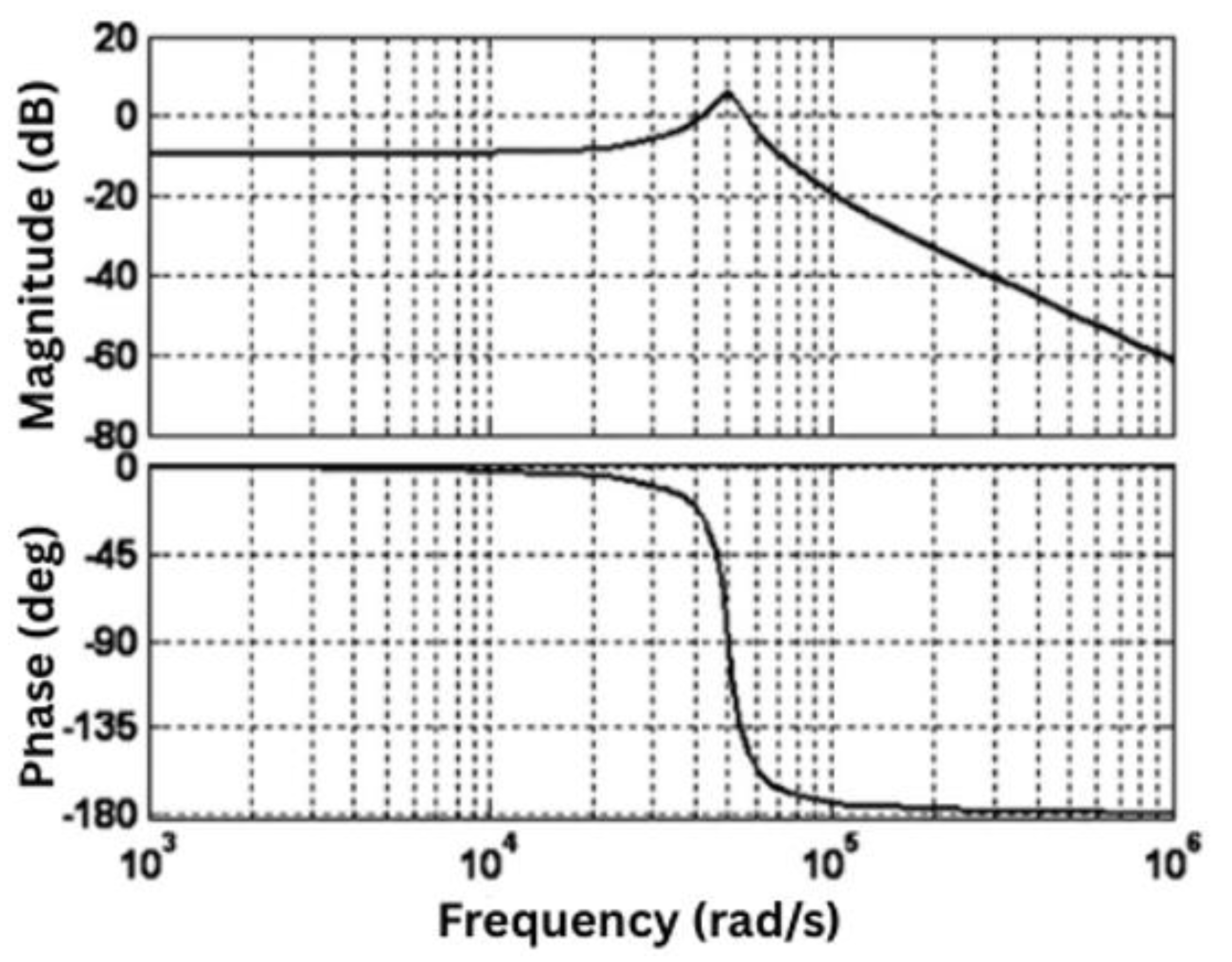
Although these two derivations differ in style, both yield a small-signal transfer function of the form
which usually has a dominant low-frequency pole set by the inductor-capacitor (LC) filter. Under ideal conditions (neglecting losses and higher-order effects), resembles a single-pole roll-off at frequencies below the switching frequency. Designers can then use classical Bode-plot methods to place compensator poles and zeros, ensuring an acceptable bandwidth and stable transient behavior. In practice, both the circuit-averaged and state-space-averaged models correctly predict where this primary LC pole and any additional parasitic poles or zeros appear.
Figure 8.
Representative Bode Plots of a Buck Converter’s Control-to-Output Transfer Function.
- 2.
- Boost Converter and the Right-Half-Plane Zero
A particularly instructive application arises with the boost converter, which often exhibits a right-half-plane (RHP) zero in its control-to-output transfer function. Whether one employs state-space averaging or circuit averaging, the linearized equations show that raising the duty cycle—intended to increase the output voltage—briefly increases the inductor current at the expense of immediate output voltage drop, causing a temporary negative dip in the output before it ultimately settles to a higher level. This behavior is mathematically characterized by a zero in the right half of the -plane. An expression frequently cited is:
where is the load resistance, is the steady-state duty ratio, and is the inductance. The presence of this RHP zero complicates feedback design because it introduces a 180-degree phase shift at higher frequencies. Both state-space and circuit-averaged models make it clear that for large , the RHP zero moves to relatively low frequency, demanding careful compensation to maintain stability and meet transient specifications.
- 3.
- Control Design Implications
Once an averaged model is obtained—regardless of the specific averaging method—engineers can construct the open-loop transfer function and design a suitable compensator. For instance, in the boost converter case, a compensator strategy might include:
- Placement of a zero well below the LC resonance to boost phase margin.
- Additional filtering to counteract high-frequency noise and mitigate the phase shift from the RHP zero.
Such design steps are directly guided by the magnitude and phase plots generated from the linearized model. In each topology, the small-signal parameters (inductance , capacitance , load , and duty cycle ) determine the poles and zeros that dominate the response, and these dominate the choice of compensation network.
Table 4.
Example Numeric Parameter Set and Resulting Small-Signal Parameters.
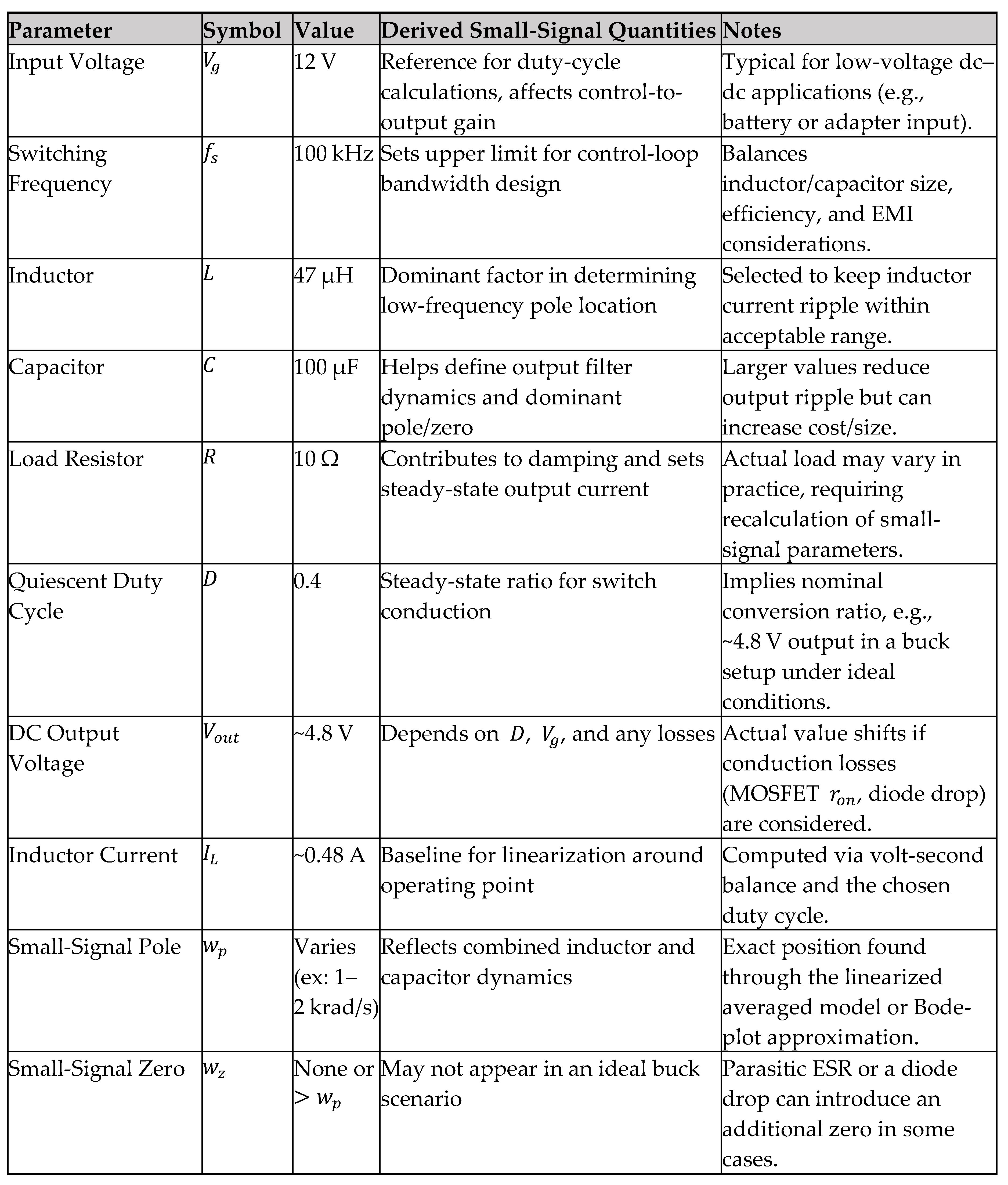 |
Remarks:
- Numerical values in this table serve as a starting point for design and analysis. In practice, parasitic elements (like transistor on-resistance, diode forward drop, or capacitor ESR) should be included to refine the small-signal predictions.
- For boost or buck-boost converters, the steady-state duty cycle and resulting output voltage would differ accordingly, and additional poles or a right-half-plane zero may arise in the transfer function.
- 4.
- Concluding Observations
Both circuit averaging and state-space averaging have proven effective for deriving small-signal AC models of converters in CCM. While circuit averaging may offer more visual insight into the role of the switch network, state-space averaging supplies a systematic procedure rooted in linear system theory. Ultimately, the two methods converge on the same essential description of converter dynamics, including the identification of significant transfer functions such as and , as well as crucial elements like the RHP zero in certain topologies. Armed with these models, designers can confidently analyze system stability, shape the loop response, and ensure that switching converters meet performance targets under a variety of operating conditions.
7. Guidelines for Implementation in Design and Simulation
Once a converter’s low-frequency model has been derived through averaging, it can be incorporated into both analytical workflows and computer-based simulations to streamline design, optimization, and verification. The following points outline a practical sequence for using averaged models effectively, while noting important considerations that help maintain accuracy.
- Selecting the Appropriate Level of Detail
At the earliest stages of design, a simplified averaged model is often sufficient to determine loop stability requirements and estimate bandwidth limitations. By removing high-frequency switching terms, the averaged approach provides concise relationships among the inductor current, capacitor voltage, duty cycle, and input variables. When higher fidelity is required, for example to capture conduction losses or parasitic components, these can be introduced into the averaged equations as additional resistive or voltage-drop elements in the relevant inductor or diode paths. If the converter operates close to boundary conditions—such as when the inductor current may become discontinuous—then an extended model or an additional subinterval (reflecting the zero-current state) must be included.
- 2.
- Implementation in Circuit Simulators and Control Tools
Modern circuit simulators (e.g., SPICE-based platforms) and system-level tools (such as MATLAB® or similar environments) both accommodate averaged models:
- Circuit Averaging in SPICE:
In a SPICE-like simulator, replace the switching elements (transistor and diode) with controlled sources or an ideal transformer whose ratios depend on the steady-state duty cycle. The rest of the circuit (inductors, capacitors, load, and input source) remains in place. Voltage and current sources in the averaged switch model can then be driven by small-signal duty-cycle variations, as outlined in the preceding chapters.
- State-Space Matrices in Control Software:
If a state-space approach was used, one typically collects the matrices
and writes the system equations in the form
By inverting if necessary, and defining a state-space object (for example, in MATLAB®), one can directly generate Bode plots, step responses, and root-locus diagrams for a variety of converter operating points.
- 3.
- Model Validation Against Switching Simulations
Although averaged models excel at capturing dynamics in the frequency range of the control loop, it is prudent to confirm the validity of key predictions by comparing them to a more detailed switching simulation:
- Time-Domain Transient Comparison:
Apply a load step or an input-voltage change in both the averaged and switching-level models. Over intervals that span several switching cycles, the averaged model’s inductor current and output voltage should closely follow the smoothed behavior seen in the detailed simulation.
- Frequency-Response Measurements:
In certain simulators, it is possible to inject a small-signal perturbation around the operating point and measure the converter’s transfer functions. These measured responses can then be compared to the transfer functions derived from the linearized averaged model, particularly in the range below one-fifth of the switching frequency, where the approximation is strongest.
- 4.
- Practical Tips for Loop Design
- Control Bandwidth Placement:
Because the averaged model omits high-frequency switching harmonics, it is most reliable for frequencies well below the switching frequency. As a rule, designers often restrict the control-loop crossover to below one-tenth (or at most one-fifth) of the switching frequency to ensure that the linear approximation remains accurate.
- Incorporating Losses and Parasitics:
When conduction losses or component parasitics significantly affect the converter’s performance, these can be introduced as additional small resistances in the inductor or transistor path, or as voltage sources modeling diode drops. The resulting corrections appear in the averaged equations as terms that slightly shift the poles and zeroes of the converter’s transfer functions.
- Discontinuous Conduction Mode:
Should the converter slip into discontinuous conduction under light-load conditions, the averaged approach outlined in earlier chapters for continuous conduction may require modification. One might add a third subinterval representing the inductor current falling to zero, leading to a different set of state equations for that portion of the cycle.
- 5.
- Summary of the Workflow
In typical practice, an engineer uses the averaged model to establish the essential controller structure and tune its key parameters, then performs a switching-level simulation to confirm that the converter behaves as expected when switching dynamics, non-ideal component behaviors, and high-frequency noise are considered. By combining these complementary perspectives, design cycles can be shortened significantly, and issues like insufficient phase margin or unexpected transient overshoots can be caught early in the development process.
In conclusion, averaged converter models provide a balanced compromise between purely ideal theoretical analyses and full-scale switching simulations. They capture the crucial LC resonance and duty-cycle modulation behavior that govern loop stability and transient performance, with enough accuracy for most control design tasks, yet retain sufficient simplicity to be readily implemented in SPICE or control-system software.
8. Conclusion
This paper has examined how fundamental concepts of state-space and circuit averaging can be leveraged to model the low-frequency behavior of switch-mode power converters under continuous conduction. By representing switching devices through their averaged impact on inductor current and capacitor voltage, designers gain an efficient way to analyze transfer functions, predict system stability, and shape the feedback loop without simulating every high-frequency event.
One of the central observations is that both averaging techniques ultimately converge on equivalent small-signal models, yielding similar poles, zeros, and steady-state relationships. This convergence underscores the reliability of averaged models for tasks such as establishing loop bandwidth targets or identifying the potential for right-half-plane zeros in boost-type converters. Moreover, the canonical representation provides a unifying viewpoint, enabling comparisons across different topologies and streamlining the design process when moving from one converter architecture to another.
While these methods work best when the converter operates in a regime with relatively small ripple and a clearly defined duty cycle, they form a solid baseline for many practical applications. More specialized approaches may be required for discontinuous conduction or more intricate switching schemes, yet the general principles described here remain directly applicable to a broad class of modern power electronic systems.
Appendix A. Extended Mathematical Derivations
Certain derivations in the main chapters may benefit from more detailed mathematical steps than those presented in the primary discussion. This appendix provides the additional detail for a nonideal buck-boost converter, incorporating the effects of finite MOSFET on-resistance and diode drops into the averaged equations.
Appendix A.1 Nonideal Buck-Boost Modeling
Consider a switching period with duty cycle . During the on-interval , the MOSFET is assumed to conduct with on-resistance while the diode is reverse-biased; during the off-interval , the diode conducts with forward voltage drop , and the MOSFET is non-conducting. For the inductor and capacitor , the averaged inductor voltage and capacitor current over one switching cycle can be summarized as follows:
where is the time-averaged inductor current, is the time-averaged capacitor voltage, and is the load resistor. In steady-state, one sets the time derivatives of and to zero, yielding two algebraic equations:
- Volt-second balance on the inductor:
- 2.
- Charge balance on the capacitor:
Appendix B. Simulation Parameters and Reference Values
For ease of replication, Table B.1 lists typical parameter values and initial operating conditions used for illustrative simulations in various converter examples:
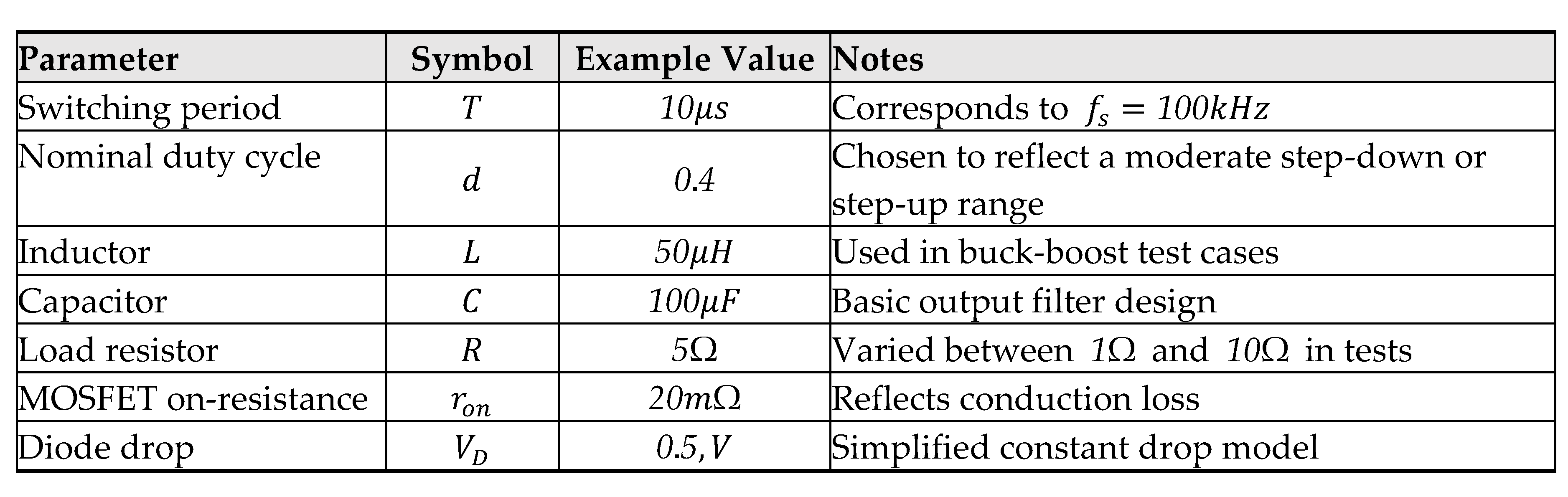
These sample values can be altered based on the specific application under study. In more refined models, the user might also include parasitic inductances, ESR in capacitors, or a more detailed diode I–V curve.
Appendix C. Additional Control Schemes
While the main chapters focus on conventional voltage-mode control under continuous conduction, many practical designs implement different strategies:
- Current-Mode Control:
The inductor current is sampled each cycle to generate an inner current loop. Averaged modeling can still be applied, but it often includes an additional control-block representation accounting for current sensing and slope compensation.
- 2.
- Discontinuous Conduction Mode (DCM):
When the inductor current reaches zero before the next switching cycle begins, an extra subinterval appears in the switch operation. The averaging process then typically involves three intervals instead of two, requiring separate derivations for each interval’s inductor voltage and capacitor current.
- 3.
- Digital or Predictive Control:
Advanced digital controllers may adjust the duty cycle based on real-time measurements or predictive algorithms. Although the underlying converter hardware can still be represented by a small-signal averaged model, the control law itself might not adhere to the linear feedback formats typically seen in analog designs. For each scenario, the principles of averaging remain consistent: identify the main energy-transfer paths, compute the averaged inductor and capacitor relations, and then derive small-signal equations by linearizing about an equilibrium point.
References
- R. W. Erickson and D. Maksimovic, Fundamentals of Power Electronics, 2nd ed. Boston, MA, USA: Kluwer Academic Publishers, 2001.
- R. D. Middlebrook and S. Ćuk, “A general unified approach to modeling switching dc-to-dc converters in continuous and discontinuous modes,” in Proc. IEEE Power Electron. Specialists Conf. (PESC), 1977, pp. 18–34.
- V. Vorpérian, “Simplified analysis of PWM converters using the model of the PWM switch—Parts I and II,” IEEE Trans. Aerosp. Electron. Syst., vol. 26, no. 3, pp. 490–505, May 1990.
- D. M. Mitchell, DC-DC Switching Regulator Analysis. New York, NY, USA: McGraw-Hill, 1988.
- G. Hua, C. S. Leu, Y. Jiang, and F. C. Lee, “Novel zero-current-transition PWM converters,” IEEE Trans. Power Electron., vol. 9, no. 2, pp. 213–219, Mar. 1994.
- H. Sira-Ramirez, “On the averaged modeling of switching regulators,” in Proc. IEEE Power Electron. Specialists Conf. (PESC), 1985, pp. 76–84.
- B. Johansson, Analysis and Design of High-Efficiency, High-Power-Factor Ballast and Power Supply Converters. Ph.D. dissertation, Dept. Ind. Electr. Eng. Autom., Lund Univ., Lund, Sweden, 2004.
- T. F. Wu and Y. K. Chen, “Modeling PWM DC/DC converters and their control loops using the PWM switch approach,” IEEE Trans. Power Electron., vol. 13, no. 3, pp. 497–505, May 1998.
- R. D. Middlebrook, “Small-signal modeling of pulse-width modulated converters,” in Proc. IEEE Power Electron. Specialists Conf. (PESC), 1976, pp. 499–507.
Disclaimer/Publisher’s Note: The statements, opinions and data contained in all publications are solely those of the individual author(s) and contributor(s) and not of MDPI and/or the editor(s). MDPI and/or the editor(s) disclaim responsibility for any injury to people or property resulting from any ideas, methods, instructions or products referred to in the content. |
© 2025 by the authors. Licensee MDPI, Basel, Switzerland. This article is an open access article distributed under the terms and conditions of the Creative Commons Attribution (CC BY) license (http://creativecommons.org/licenses/by/4.0/).
Copyright: This open access article is published under a Creative Commons CC BY 4.0 license, which permit the free download, distribution, and reuse, provided that the author and preprint are cited in any reuse.


