
Submitted:
29 April 2025
Posted:
29 April 2025
You are already at the latest version
Abstract
In this paper, we derive a model for surface temperature variations on the non-illuminated side of a thermally thin semiconducting sample exposed to an optical pulse, incorporating the contribution of surface charge carrier recombinations to semiconductor heating. Based on this model, we analyze the influence of surface recombination velocity and the semiconductor’s plasma properties on the time-domain temperature change at non-illuminated side of semiconducting sample for both plasma-opaque and plasma-transparent samples. Our results show that charge carrier recombinations can have a significant impact on the time-resolved photoacoustic signal recorded with minimum volume cell, suggesting that photoacoustic measurements could be used to determine the electronic properties of semiconductors.
Keywords:
time domain photoacoustic
; minimum volume cell
; semiconductors
; plasma effects
; surface recombinations
1. Introduction
Frequency photoacoustics (PA) of semiconductors and semiconductor devices has been developing for over four decades, with the goal of enabling non-destructive characterization of optical, thermal, elastic, and electronic properties essential for the design of various microelectronic, photonic, sensor, and biosensor devices, as well as solar cells and thermal management of VLSI circuits [1,2,3,4,5,6,7,8,9,10,11]. Previous studies have demonstrated that frequency-domain PA spectroscopy [12] can be used to measure various physical properties of semiconductors. However, these methods are not suitable for real-time measurements, which are crucial for many industrial and biomedical applications [13]. On the other hand, the development of time-domain PA methods [14,15,16,17] provides this capability but requires advancements in time-resolved models and signal processing techniques based on them [16]. In this paper, we focus on developing a model of the PA signal for time-domain photoacoustics of semiconductors, utilizing insights gained from the development of frequency-domain photoacoustics.
There are three different approaches to modeling the photothermal and photoacoustic effects in semiconductors. The first approach is based on the assumption that photogenerated carriers influence the thermal conductivity, diffusivity and/or thermal relaxation time of a semiconductor sample exposed to electromagnetic radiation [18,19,20,21], and through these properties, they affect the temperature distribution within the sample, consequently impacting the thermoelastic bending of the sample and pressure fluctuations in the surrounding gaseous medium. The second approach relies on the two-temperature model of the interaction between the excitation optical beam and the semiconductor sample [22,23,24,25] and can be particularly suitable for highly doped, degenerate semiconductor samples. The third approach, which will be used in this study, assumes that two types of heat sources emerge within a semiconductor upon illumination [12,26,27,28]. The first type is characteristic of all solid-state materials and can be referred to as fast heat sources. These sources arise due to the interaction of the excitation electromagnetic radiation with lattice vibrations and non-radiative de-excitation relaxation processes, which convert the absorbed electromagnetic energy into heat. Since non-radiative de-excitation relaxation processes occur over extremely short timescales—much shorter than those relevant for observing photothermal effects—the time dependence of these heat sources can be considered to follow the time dependence of the excitation optical irradiance. However, due to the band structure of semiconductors, which includes a partially filled valence band, a partially empty conduction band, and a bandgap in between, the interaction of excitation photons with charge carriers leads to the photogeneration of quasi-free charge carriers if the photon energy exceeds the semiconductor’s bandgap width [29]. When an electron is excited from the valence band, it leaves behind a positively charged vacancy, known as a hole. Electron-hole pairs, bound by Coulomb interaction, diffuse through the semiconductor due to the established concentration gradient and recombine after a characteristic period known as the carrier lifetime. During recombination, they transfer their kinetic energy to the crystal lattice, forming so-called slow heat sources at the recombination sites within the semiconductor [12]. The resulting temperature distribution in the illuminated semiconductor can be described as a superposition of temperature variations originating from both slow and fast heat sources. From a physical perspective, this approach is particularly suitable for narrow-bandgap semiconductors that are moderately doped, ensuring that the Fermi level remains within the bandgap. From the perspective of photoacoustic research and its applications in semiconductor and semiconductor device characterization, this approach is the most appropriate because it describes the relationship between photogenerated plasma, the electronic properties of semiconductors, optical heating of the sample, and the measurable photoacoustic signal [12,26,27,28].
In this study, we investigate how photo-induced quasi-free carriers affect surface temperature variations in a thin, moderately doped semiconductor sample when illuminated by square optical pulses. To analyze these effects, we use some of the parameters introduced in our previous papers [16,30] on time-resolved PA signals: rise time, fall time, settling time, and the stationary value of the signal. These parameters, commonly used in system dynamics, automatic control, and signal transmission and processing (telecommunications), help establish a connection between the time-dependent signal and the parameters of the system through which the signal propagates.
The structure of the paper is as follows. After this introduction, Section 2 derives a model of photothermally induced temperature changes at the non-illuminated surface of a thin semiconductor sample, generated by fast and slow thermal sources, using the Laplace transform method and electro-thermal analogy. In Section 3, we analyze the influence of sample thickness, surface recombination velocities and electronic properties on the time-domain PA response for a thermally thin semiconductor sample. Finally, the key conclusions are summarized in Section 4.
2. Photoinduced heat transfer across thin semiconductor: Theoretical model
The model of photoinduced heat propagation is derived under the following assumptions:
The sample is excited by an optical pulse of irradiance I(t) [W/m2], where f(t) describes the time dependence of the incident irradiance:
With h(t) is denoted the Heaviside step function and with T [s] the pulse duration
Before the excitation of optical radiation, the whole structure and its environment were at the same temperature – Тamb [K].
The deexcitation-relaxation processes due to photon-phonon interactions are assumed to be much faster than the rate of change of the rising edge of the optical pulse. Thus, the heat sources formed by these processes follow the temporal shape of the optical pulse [31].
We consider a semiconductor disk uniformly illuminated across its cross-sectional surface normal to the direction of light propagation (Figure 1), allowing the entire problem of optically generated heat propagation to be analyzed using a one-dimensional approximation [32].
It is assumed that the surrounding gas does not absorb the incident radiation. Heat sources are generated solely within the sample; however, the resulting thermal disturbance affects the surrounding area.
The sample is considered optically opaque, i.e. where is the optical absorption coefficient [1/m] and ls [m] is the sample thickness. Thus, the excitation optical beam penetrates only a thin layer of the semiconductor near its illuminated surface. The optically generated heat due to photon-phonon interactions can be described as a surface heat source [32,33]:
where R is the sample’s reflectance and δ is the Dirac delta function.
The contribution of volume recombinations of semiconducting sample is neglected, and heat sources caused by surface recombination can be described by [12,26,27,28]:
where , , , , and are parameters describing the surface recombination velocity at the illuminated (g) and non-illuminated (b) surfaces of the semiconductor sample, the concentration of photoinduced minority carriers at the sample surfaces, and the energy gap of the semiconductor, respectively.
The semiconductor sample is surrounded by air, which is a much poorer thermal conductor than the semiconductor itself. Therefore, adiabatic boundary conditions for the heat flux are assumed [35].
Nonlinear effects in heat conduction and the transport of photogenerated charge carriers through the semiconductor, as well as thermal relaxation effects, are neglected because these effects are not expected to be significant in photoacoustic experiments.
Under these assumptions, the conduction of photogenerated heat through the semiconductor sample can be described by the one-dimensional classical Fourier’s theory of heat conduction [36], leading to the following system of linear partial differential equations:
with inhomogeneous boundary conditions [12]:
and zero initials conditions.
In above equations (Eqs 5-8) with is denoted the temperature variations in relation to ambient (initial) temperature, .
Since the problem is linear, the temperature distribution in the illuminated semiconductor sample can be obtained by applying the Laplace transform to Eqs. (5)–(8). In this case, the system of equations (5)–(8) reduces to a system of ordinary differential equations in the complex domain:
with following boundary conditions:
In Eqs. (9)–(12), the variables with an overline denote the Laplace transforms of the temperature, heat flux, the time function describing the modulation of the excitation beam’s amplitude, and the recombination heat sources on the illuminated and non-illuminated surfaces. With is denoted complex frequency.
Symbols represent the complex coefficient of heat propagation and thermal impedance, respectively, defined as follows:
As can be seen from Eqs. (9)–(10), heat propagation through the semiconductor sample is described by equations analogous to those governing the propagation of current and voltage through an electrical transmission line [37,38], (see Figure 2) with the propagation coefficient and characteristic impedance that can be defined as
With symbols and are denoted complex series impedance and complex parallel admittance of transmission line segment (Fig2)
As can be seen from the boundary conditions (11)–(12), heat propagation is driven by surface heat fluxes, which is analogous to the excitation of an electrical transmission line by current sources (boundary conditions (11)–(12):
To calculate surface temperature variations on the unilluminated side, it is convenient to use the representation of an electrical transmission line via a symmetrical electrical T-network with two ports (quadripole) [37,38,39,40,41,42,43]. The analogous electrical circuit for calculating surface temperature variations on the unilluminated surface is shown in Figure 3.
The impedances of the equivalent electrical circuit shown in Figure 3 are given by the expressions [37,39]:
where and denote the equivalent longitudinal impedance and the equivalent longitudinal admittance, respectively:
while the equivalent current sources are given by the following expression:
Symbols , and signify the spectral function of concentrations of minority charge carriers at illuminated and non-illuminated surfaces, respectively while with si i=g,b are denoted the surface recombination velocity at corresponding surface i: g-illuminated and b non-illuminated.
Spectral functions of charge carrier concentrations are obtained by solving diffusion equation for minority charge carriers [12,28] (see Appendix A):
In the above equations, E denotes the energy of the exciting photons, which depends on the wavelength of the optical excitation, while and (see Appendix 1) represent complex functions that depend on the electronic properties of minority carriers (diffusion coefficient and lifetime), surface recombination velocities sg and sb, and the ratio of the sample thickness ls to the maximum diffusion length of minority carriers μmax (see Appendix A)[28].
By substituting Eqs 28 and 29 into Eqs. 26 and 27, a mathematical description of the spectral functions of recombination heat sources in the illuminated semiconductor is obtained:
As can be seen from Eqs 30 and 31, the recombination sources can be described as a convolution of the function that represents the thermalization source and the functions Gg(t) or Gb(t), which depend on the diffusion of minority carriers in the semiconductor.
By applying the superposition principle in solving the circuit shown in Figure 3, we obtain the spectral functions of the total temperature variations on the unilluminated surface as a sum of temperature variations generated by each of the sources described in equations (25), (30), and (31):
It is important to note that there are two limiting cases considering frequency of excitation harmonic: the thermally thin sample () and the thermally thick sample ().
Considering definition of (Eq. 13) the following relation is obtained:
From the above equation (Eq. 33), it can be easily concluded that for low frequencies, below a certain cutoff frequency fc (which depends on ls and DT), every sample is thermally thin. Conversely, for high frequencies, above the cutoff frequency fc, every sample is thermally thick, where fc is given by:
In further considerations, we will assume that the sample is geometrically thin, so that the excitation harmonics span a wide frequency range and the sample is thermally thin. In this case, the equivalent circuit from Figure 3 is reduced to the equivalent circuit shown in Figure 4 [37].
By solving the circuit shown in Figure 4, we obtain the spectral functions of surface temperature variations caused by photon-lattice interactions, as well as the spectral functions of temperature variations resulting from surface recombination of photogenerated excess charge carriers (Eqs. 35-37):
By substituting Eqs 24 and 25 into Eq 35, the spectral function of surface temperature variations caused by lattice thermalization at the non-illuminated side of the semiconductor sample exposed to the action of a square optical pulse of duration T is obtained:
By substituting Eqs 24, 30, and 31 into Eqs 36, 37, the spectral function of surface temperature variations due to recombination sources at the surface of the semiconductor, is obtained:
Considering heat sources generated by recombinations of minority carriers at sample surfaces depend on ratio of the sample thickness and diffusion length of minority carries i.e. plasma transparence [28], we further observe two limiting cases : the case thermally thin and plasma opaque and the case of thermally thin and plasma transparent sample.
2.1. Surface Temperature Variations in Thermally Thin and Plasma Opaque Semiconductor Sample
The spectral functions of recombination heat sources in plasma opaque samples are given by [28]:
where
Symbols and signify the diffusivity of minority charge carriers and their lifetime, respectively (see Appendix1).
In that case, the temperature variations generated by surface recombination become:
By finding inverse Laplace transform of Eq 44, we obtain (see Appendix 2)
where function g1 is defined by:
and
2.2. Surface Temperature Variations in Thermally Thin and Plasma Transparent Semiconductor Sample
The spectral functions of recombination heat sources in plasma transparent samples are given by [28]
Parameters r1, r2, p, and q are defined by the following expressions:
By substituting expressions (50) and (51) into equation (39), we obtain the spectral function of temperature variations in a thermally thin and plasma-transparent semiconductor sample, caused by surface recombination heat sources:
with parameter r3 defined by
By finding inverse Laplace transform of Eq 56, (see Appendix2) we obtain:
with function g2(t) defined by
3. Analyzes and Discussion
The PA measurements with a minimal volume cell record pressure fluctuations in the gas column located on the non-illuminated side of the sample. The measurement configuration is transmission-based, as the source and detector are on opposite sides of the sample being examined [47]. Literature indicates that in this type of measurement configuration, the spectral function of resulting pressure fluctuations in the closed cell can be described by a composite piston model [48]. Specifically, these pressure fluctuations are a consequence of the thermal piston effect, which involves the expansion and contraction of the thin layer of air adjacent to the illuminated surface of the sample [49,50]. Additionally, the bending of the sample surface due to the generation of a thermal moment within the sample [48] acts as a mechanical piston, producing the thermoelastic (TE) component of the PA response.
In semiconductors, due to the photogeneration of charge carriers, there exists a plasma-elastic component resulting from the bending of the sample surface caused by the concentration gradient of excess charge carriers in illuminated semiconductor samples [12,51]. If the sample is thin, both the TE and plasma-elastic components can be neglected [16,52]. In that case, it can be assumed that the pressure fluctuations are caused solely by the thermal piston effect and are consequently proportional to the surface temperature variations [52,53,54,55].
However, the thermal piston model is not suitable for time-domain photoacoustics [16,30,56,57,58]. In this case, it is more appropriate to use models derived in [16,30,56,57,58], which also indicate that temperature changes at the non-illuminated surface generate pressure variations in a closed PA cell. However, the thermal thickness of the gas column in the closed PA cell [30] and the transfer characteristics of the microphone [16,30] can alter the time profile of the recorded time-resolved electrical signal.
In this study, we analyze the evolution of temperature changes at the non-illuminated surface and the influence of photogenerated charge carriers on the magnitude and slope of these changes based on the derived model (hereafter referred to as the time-domain temperature signal). However, modeling the transfer function of the gas column () and the microphone (), which is essential for a complete understanding and accurate processing of the recorded time-resolved PA signal in semiconductors [17], remains the focus of our future research.
In the calculations, it was assumed that the excitation occurs in the visible part of the electromagnetic spectrum meaning E/EG for narrow gap semiconductors such as Si is equal to unity [12]. The normalized components were considered relative to the constant .
The parameters of the silicon sample used in the calculations are provided in Table 1.
In the analysis, it was also assumed that the pulse duration is 50 ms, as impulses of this duration are used in real time-domain PA experiments [16,17].
Let us consider the thicknesses of the Si sample for which the assumptions of the derived model are satisfied.
The optical absorption coefficient of silicon is 105 m−1 for light from the visible part of the electromagnetic spectrum [34]. Consequently, the approximation of optically opaque sample is reasonable for silicon samples thicker than .
Since the thermal diffusivity of silicon is 9·10-5 m2s −1 [12], the cutoff frequency between thermally thin and thermally thick regimes for a sample with a thickness larger than 10 μm can be calculated from Eq. (34). It ranges from approximately 5 kHz for a 90 µm thick sample to 300 kHz for a 10 µm thick sample. For samples which thickness is about 100 µm, the cutoff frequency varies from 50 Hz for a 900 µm thick sample to 3000 Hz for a 100 µm thick sample. This implies that in the PA measurement range (from 50 Hz to a few kHz), silicon samples with a thickness of 10-150 µm can be considered as thermally thin.
Finally, in our model, we considered two cases related to the ratio of the maximum diffusion length of minority carriers to the geometric thickness of the sample. These are the case of a plasma-opaque sample, when this ratio is less than one, and the case of a plasma-transparent sample, when this ratio is greater than one.
Since the maximum diffusion length of minority carriers is given by the square root of the product of their diffusion coefficient and lifetime (see Appendix 2), it can be estimated based on the parameters given in Table 1 that a p-doped silicon sample with a thickness greater than 135 is plasma-opaque, while an n-doped silicon sample is plasma-opaque if it is thicker than 75. This means that Si samples, whether p- or n-doped, with a thickness below 75 are plasma-transparent, whereas samples thicker than 135 are plasma-opaque.
In the further analysis, we considered silicon samples with a thickness of 20 as representatives of plasma-transparent, thermally thin, and optically opaque semiconductor samples, and samples with a thickness of 140 as representatives of plasma-opaque, thermally thin, and optically opaque semiconductor samples.
Figure 5 shows the normalized time domain temperature signal (evolution of temperature change on the non-illuminated side) for a thermally thin, plasma-opaque n-doped silicon sample (ls = 140 µm, Dp = 1.2 × 10⁻³ m²/s). The red line represents the signal originating from lattice thermalization (fast thermal source), while the blue lines correspond to signals influenced by surface recombination for different values of sg. The green lines depict the total signal resulting from both sources. (Legend: sg = 6 m/s (solid line), sg = 10 m/s (dashed line), sg = 14 m/s (dash-dot line)).
As shown in Figure 5, in plasma-opaque and thermally thin samples, carrier recombination does not alter the shape of the signal but does affect its maximum value (blue and green lines). When paremeter sg is low (below 6 m/s) the contribution of recombination sources is negligible and the signal is primarily determined by lattice thermalization (solid red and green lines). However, as sg increases, recombination effects become more significant. For sg = 14 m/s, recombination sources play a dominant role in temperature change (dash-dot green and blue lines in Figure 5).
From Figure 5, it can also be observed that the time domain temperature signal for a thermally thin semiconductor sample reaches a steady value of zero after a time equal to 2T. This indicates that the settling time is equal to twice the duration of the optical pulse.
In cases where the signal does not reach a peak during the pulse duration, it is not appropriate to work with parameters such as rising time or falling time; instead, it is much more suitable to consider the slope of the rising or falling curve. Figure 5 shows that the slopes of the rise after the leading edge of the excitation and the slope of the fall after the trailing edge of the pulse are equal and depend on the surface recombination velocities.
To investigate the impact of the charge carrier diffusivity (the semiconductor electronic property) on the shape of the time-domain temperature signal, Figure 6 presents the signal for a thermally thin and plasma-opaque p-doped Si sample (ls=140 µm, De=3.6×10⁻³ m2/s,). The red line represents the signal resulting from lattice thermalization (fast heat source), while the blue lines indicate the signal from surface recombinations at different sg values. The green lines show the total signal caused by both sources: sg=6m/s (solid lines), sg=10m/s (dashed lines), and sg=14m/s (dash-dotted lines).
As seen in Figure 6, for the plasma-opaque and thermally thin p-doped sample, the recombination of charge carriers similarly affects the time domain temperature signal as in the n-doped sample (Figure 5). Specifically, it does not influence the shape or settling time, but it does impact the maximum value of the signal in the time domain (indicated by the blue and green lines in Figure 5 and Figure 6) and the slopes of both the rising and falling curves.
However, in the case of the p-doped sample, minority carriers are electrons, which have a diffusion coefficient three times larger (as shown in Table 1). Therefore, at the same surface recombination velocities, the dominance of recombination sources does not occur for the sg>10 m/s (Figure 6).
Based on this observation, it can be concluded that the slopes of the time-domain temperature signal—both the rising slope following the leading edge of the optical pulse and the falling slope following the trailing edge—are influenced by the electronic properties of the semiconductor, particularly the diffusion coefficient of the minority carriers. The increase in diffusion coefficient affect slower rising and falling of the signal and consequently smaller maximal value of the signal for the same surface recombination velocities.
It is interesting to note that the results presented in Figure 5 and Figure 6 indicate that the complex function describing the time-domain temperature signal in thermally thin and plasma-opaque samples (Eq 47) can, in fact, be approximated by a linear function. The electronic parameters of silicon (such as the minority carrier lifetime and their diffusion coefficient) primarily influence the slope of the linear function.
Figure 7 illustrates the normalized time-domain temperature signal for a thermally thin and plasma-transparent n-doped silicon sample (with ls=20µm and Dp=1.2×10⁻³ m2/s). The red line represents the signal originating from thermalization of the lattice (a fast heat source), while the blue lines show the signal resulting from surface recombinations for sb=6m/s and various sg values. The green lines depict the total signal generated by both sources (sg=6 m/s a solid line and sg=14 m/s as a dashed line)
As seen in Figure 7, the time-domain temperature signal from the plasma-transparent sample behaves similarly to that of the plasma-opaque sample in terms of shape, settling time, and dependence on sg. However, for the plasma-transparent sample, the rise and fall slopes are also influenced by the surface recombination velocity sb. This results in a slower rise of the signal, leading to significantly lower maximum signal values when all other electronic and thermal parameters remain constant if the sample is plasma transparent.
To further investigate the impact of sb, Figure 8 presents the time-domain temperature signal for a thermally thin and plasma-transparent n-doped silicon sample (ls=20µm, Dp=1.2×10⁻³ m2/s) with a fixed sg=2 m/s. The value of the surface recombination velocity on the unilluminated side, sb, was varied. The red line indicates the signal resulting from thermalization of the lattice (a fast heat source), while the blue lines show the signal from surface recombinations for sg=2 m/s at different sb values. The green lines represent the total signal caused by both sources, with sb=6 m/s indicated by a solid line and sb=24 m/s by a dashed line.
As seen in Figure 8, the increase in sb influences both the slope of the time-domain temperature signal and the maximum value the signal reaches just before the falling edge of the optical pulse, similar to the effect observed with an increase in sg.
Finally, Figure 9 presents the normalized time-domain temperature signal for a thermally thin and plasma-transparent p-doped Si sample (with ls=20 μm and Dp=3.6×10⁻³ m2/s) at sg=2m/s, sb=2m/s and sg=24m/, sb=24m/s. This analysis aims to investigate the influence of the electronic properties on time domain temperature signal of the thermally thin and plasma transparent semiconductor sample.
By comparing the results shown in Figure 8 and Figure 6, it is evident that an increase in the diffusion coefficient of minority carriers, similar to the case of plasma-opaque samples, influences both the maximum value that the time-domain temperature signal can achieve during the pulse duration and the steepness of the nearly linear rising and falling curves. However, this increase does not affect the settling time.
4. Conclusions
In this paper, a model for temperature change on the non-illuminated side of thermally thin semiconductors exposed to a rectangular optical pulse has been developed. This model incorporates the impact of surface recombination of photo-generated charge carriers at the semiconductor surfaces.
Based on the derived model, the influence of recombination sources and the electronic properties of semiconductors on surface temperature evolution have been analyzed using moderately n- and p-doped silicon samples as examples.
It has been demonstrated that, depending on the surface recombination velocity (which is influenced by the surface processing methods of the samples), recombination sources can significantly affect the magnitude of the surface temperature change and the slopes of its rise and decay, compared to the effect of lattice thermalization. The dominant influence of recombination sources is observed in plasma-opaque samples with high surface recombination velocity at the illuminated surface.
At low surface recombination velocities, lattice thermalization is the dominant mechanism of sample heating and influence of recombination sources can be neglected in plasma-opaque and thermally thin samples. In plasma-transparent samples, although recombination does not dominate over lattice thermalization, it remains significant at both low and high surface recombination velocities.
Furthermore, the electronic properties of the semiconductor affect the slope of the rising and falling temperature signal and its maximum value but do not influence the overall shape of the signal or the settling time.
Our results show that charge carrier recombination can have a significant impact on the temperature change at the non-illuminated side of a semiconductor sample and, consequently, on the time-domain PA signal. The observed dependence of time-domain temperature signal on the sample thickness, surface processing, and diffusion coefficient of minority charge carriers suggests that this technique could be used to determine the electronic properties of semiconductors.
For a complete understanding and accurate processing of experimentally recorded time-resolved PA signals in thin semiconductor membranes [17], further investigation are required to understand the transformation of non-periodic temperature changes at the sample surface into pressure fluctuations and the subsequent conversion of these fluctuations into an electrical signal. This remains the subject of our ongoing research.
Author Contributions
Conceptualization, S.G; methodology, S.G; software, S.G.; validation, S.G. M.P. D.M.T.; formal analysis, S.G, D.K.M, D.D.M, K.Dj. M.P. E.S. investigation, S.G, D.K.M, D.D.M, K.Dj. M.P.,E.S; D.M.T resources, S.G, E.S; data curation, S.G, D.M.T.; writing—original draft preparation, S.G.; writing—review and editing, S.G, K.Dj. M.P. D.M.T.; visualization, S.G, K.Dj.; supervision, D.M.T, E.S; project administration, S.G, E.S.; funding acquisition, S.G, E.S All authors have read and agreed to the published version of the manuscript.
Funding
This research was funded by Ministry of Science, Technological Development and Innovations of the Republic of Serbia (Contract No. 451-03-136/2025-03/ 200017).
Institutional Review Board Statement
Not applicable.
Informed Consent Statement
Not applicable.
Data Availability Statement
Data will be made available on request.
Conflicts of Interest
The authors declare no conflicts of interest.
Appendix A: Photogenerated Diffusion of Charge Carriers in Semiconductor
The equation describing the transport of photogenerated charge carriers in a semiconductor, under the low-level injection approximation, is a linear, one-dimensional spatial diffusion equation for minority carriers. By applying the Laplace transform, this equation is reduced to the second-order differential equation in the complex domain [12].
In the case where optical absorption occurs in a thin layer near the illuminated semiconductor surface (i.e. when the sample is optically opaque and has a high optical absorption coefficient), the transport problem of photogenerated charge carriers is described by the following system of homogeneous differential equations (A1-1 and A2-1) with inhomogeneous boundary conditions (A3-1 and A4-1) [28].
In the above equations, with is signified the concentration of minority charge carriers, denotes the spectral function of optically generated source of excess carriers, I0 is irradiance of excitation optical beam, and E is phonon energy. Symbols sg and sb signify the velocities of surface recombinations on illuminated (g) and non-illuminated (b) surfaces, while is coefficient of diffusion of minority charge carriers, electrons in p-doped semiconductors, or holes in n-doped semiconductor. With is denoted the inverse coefficient of propagation of charge density and it is defined by following expression [12,59]:
Symbol signify the lifetime of charge carriers in semiconductor [29,60]. With symbol i is denoted the imaginary unity.
The real part of inverse complex coefficient of propagation is diffusion length of charge carrier [28,60]
As can be seen from Eq A6-1, the carrier diffusion length depends on the frequency of the harmonic excitation. As the frequency increases, the diffusion length decreases to zero, while for a frequency of zero, it reaches its maximum value of [28,60]:
If the sample thickness is much greater than the maximum diffusion length, the sample is plasma opaque. Conversely, if the sample thickness is smaller than the maximum diffusion length, the sample is plasma transparent [28].
By solving the problem described by Eq (A1-1 )–(A4-1), the following expressions for the surface concentrations of photogenerated minority carriers are obtained:
Based on Eqs A8-1 and A9-1, approximate expressions for the surface concentrations of photogenerated carriers in plasma-opaque and plasma-transparent semiconductor samples can be easily derived [28]
Appendix B: Inverse Laplace Transform: Method of Partial Fraction and Irrational Function
To obtain evolution of some function which spectral function is known, one should solve inverse Laplace transform. Inverse Laplace transform of functions of complex argument is defined by [61]:
The integral formula given by Eq A2-1 is called the Bromwich integral, or Mellin’s inverse formula or the Fourier–Mellin integral. In many problems, computing the complex integral can be done by using the Cauchy residue theorem.
In practice, it is not necessary to solve the complex integral given by Eq A2-1 always. Instead, it could be used existing solutions given in tables inverse Laplace transforms [62] and various methods of representation of a complex function by functions which Bromowich integral solutions are known, such as method partial fractions for rational function of complex argument s [28. 62, 63].
For solving the inverse Laplace transform of the irrational function obtained in this study, the known solutions given in Table A1 were used. [64].

Table A1.
Solved inverse Laplace transform of irrational function [64].
Table A1.
Solved inverse Laplace transform of irrational function [64].
| Complex Function | Inverse Laplace Transform |
|---|---|
References
- Zakrzewski, J.; Pawlak, M.; Matsuda, O.; Todorovic, D.; Liu, J. Semiconductor physics: Plasma; thermal; elastic, and acoustic phenomena. J. Appl. Phys. 2024, 136, 120401. [Google Scholar] [CrossRef]
- Todorović, D.M. Plasma; thermal, and elastic waves in semiconductors. Rev. Sci. Instrum. 2003, 74, 582–585. [Google Scholar] [CrossRef]
- Miranda, L.C.M. Theory of the photoacoustic effect in semiconductors influence of carrier diffusion and recombination. Appl. Opt. 1982, 21, 2923–2928. [Google Scholar] [CrossRef] [PubMed]
- Isaiev, M.; Kuryliuk, V.; Kuzmich, A.; Burbelo, R. Photothermal Transformation In Heterogeneous Semiconductors Structures Under Its Pulse Laser Irradiation: Role Of Electron-Hole Diffusion. Arch. Metall. Mater. 2013, 58, 1351–1354. [Google Scholar] [CrossRef]
- Lishchuk, P.; Andrusenko, D.; Isaiev, M.; Lysenko, V.; Burbelo, R. Investigation of Thermal Transport Properties of Porous Silicon by Photoacoustic Technique. Int. J. Thermophys. 2015, 36, 2428–2433. [Google Scholar] [CrossRef]
- Bychto, L.; Maliński, M.; Chrobak, L.; Zakrzewski, J.; Boumhamdi, M. Investigations of optical and thermal properties of surface layers of Cd1−xBexTe samples by the photoacoustic method. OPTO-ELECTRON REV 2024, 32, e150186. [Google Scholar] [CrossRef]
- Zakrzewski, J.; Maliński, M.; Bachiri, A.; Strzałkowski, K. Photothermal determination of the optical and thermal parameters of CdxZn1-xSe mixed crystals. J. Mater. Sci. Eng. B 2021, 271, 115305. [Google Scholar] [CrossRef]
- Todorovic, D.M.; Cretin, B.; Song, Y.Q.; Vairac, P. Photothermal elastic vibration method: Investigation of the micro-electro-mechanical-systems. J Phys Conf Ser 2010, 214, 012105. [Google Scholar] [CrossRef]
- Cyr, B.V.S.; Long, Y.; et al. How Lasers Exploit Photoacoustic and Photoelectric Phenomena to Inject Signals into MEMS Microphones. 2024; Preprint. [Google Scholar] [CrossRef]
- Todorovic, D.; Nikolic, P. Investigation of carrier transport processes in semiconductors by the photoacoustic frequency transmission method. Optical Engineering 1997, 36, 432–445. [Google Scholar] [CrossRef]
- Pawlak, M.; Pal, S.; Wieck, A.D. On the infrared absorption coefficient measurement of thick heavily Zn doped GaAs using spectrally resolved modulated photothermal infrared radiometry. J. Appl. Phys. 2017, 122, 135109. [Google Scholar] [CrossRef]
- Todorović, D.M.; Nikolić, P.M. Semiconductors and Electronic Materials Progress in Photothermal and Photoacoustic, Science and Technology Chapter 9; Optical Engineering Press: New York, NY, USA, 2000; Volume PM74, pp. 273–318. ISBN 9780819435064. [Google Scholar]
- Sarode, A.P.; Mahajan, O.H. Theoretical Aspects of Photoacoustic Effect with Solids: A Review. IJSART 2018, 4, 1237–1242. [Google Scholar]
- Telenkov, S.; Mandelis, A. Signal-to-noise analysis of biomedical photoacoustic measurements in time and frequency domains. Rev. Sci. Inst. 2010, 81, 124901. [Google Scholar] [CrossRef] [PubMed]
- Lashkari, B.; Mandelis, A. Comparison between pulsed laser and frequency-domain photoacoustic modalities: Signal-to-noise ratio, contrast, resolution, and maximum depth detectivity. Rev. Sci. Inst. 2011, 82, 094903. [Google Scholar] [CrossRef] [PubMed]
- Galovic, S.P.; Stanimirovic, I.; Djordjevic, K.L.; Milicevic, D.; Suljovrujic, E. Time-resolved photoacoustic response of thin solids measured using minimal volume cell. Int. Commun. Heat Mass Transf. 2024, 155, 107574. [Google Scholar] [CrossRef]
- Djordjevic, K.L.J.; Galovic, S.P.; Nesic, M.V.; Todorovic, D.M.; Popovic, M.N.; Markushev, D.D.; Markushev, D.K. Transmission pulse photoacoustic set-up for characterization of solids. In Proceedings of the 21st International Symposium INFOTEH-JAHORINA, 16–18 March 2022. [Google Scholar]
- Gärtner, W.W. Photothermal Effect in Semiconductors. Phys. Rev. 1961, 122, 419–424. [Google Scholar] [CrossRef]
- Fournier, D.; Boccara, C.; Skumanich, A.; Amer, N.M. Photothermal investigation of transport in semiconductors: Theory and experiment. J. Appl. Phys. 1986, 59, 787–795. [Google Scholar] [CrossRef]
- Forgot, B.C.; Fournier, D. Photothermal characterization of semiconductors. In Progress in Photothermal and Photoacoustic Science and Technology; Chapter 7; Mandelis, A., Hess, P., Eds.; SPIE Press: Washington, DC, USA, 2000; Volume 4, p. 200. ISBN 9780819435064. [Google Scholar]
- Stanimirović, Z.; Stanimirović, I.; Galović, S.; Djordjević, K.; Suljovrujić, E. Transmission pulse photoacoustic response of thin semiconductor plate. J. Appl. Phys 2023, 133, 195701. [Google Scholar] [CrossRef]
- Titov, O.Y.; Gurevich, Y.G. Recombination and temperature distribution in semiconductors. Semicond. Sci. Technol. 2012, 27, 055014. [Google Scholar] [CrossRef]
- Titov, O.Y.; Gurevich, Y.G. Temperature gradient and transport of heat and charge in a semiconductor structure. J. Low Temp. Phys. 2021, 47, 550–554. [Google Scholar] [CrossRef]
- Sobolev, S.L. Nonlocal two-temperature model: Application to heat transport in metals irradiated by ultrashort laser pulses. Int. J. Heat. Mass. Transf. 2016, 94, 138–144. [Google Scholar] [CrossRef]
- Sobolev, S.L.; Dai, W. Heat Transport on Ultrashort Time and Space Scales in Nanosized Systems: Diffusive or Wave-like? Materials 2022, 15, 4287. [Google Scholar] [CrossRef] [PubMed]
- Mandelis, A. Laser infrared photothermal radiometry of semiconductors: Principles and applications to solid state elec-tronics. Solid•State Electron. 1998, 42, 1–15. [Google Scholar] [CrossRef]
- Rojas-Trigos, J.B.; Calderón, A.; Marín, E.A. Practical model for the determination of transport parameters in semiconductors. J. Mater. Sci. 2011, 46, 7799–7805. [Google Scholar] [CrossRef]
- Galovic, S.; Djordjevic, K.; Dragas, M.; Milicevic, D.; Suljovrujic, E. Dynamics of Photoinduced Charge Carrier and Photothermal Effect in Pulse-Illuminated Narrow Gap and Moderate Doped Semiconductors. Mathematics 2025, 13, 258. [Google Scholar] [CrossRef]
- Wang, S. Fundamentals of Semiconductor Theory and Device Physics; Prentice Hall, Inc.: Hoboken, NJ, USA, 1989; ISBN 0-13-344425-2. [Google Scholar]
- Galovic, S.P.; Djordjevic, K.L.; Nesic, M.V.; Popovic, M.N.; Markushev, D.D.; Markushev, D.K.; Todorovic, D.M. Time-domain minimum-volume cell photoacoustic of thin semiconductor layer. I. Theory J. App. Phys. 2023, 133, 245701. [Google Scholar] [CrossRef]
- Sablikov, V.A.; Sandomirskii, V.B. The Photoacoustic Effect in Semiconductors. physica status solidi (b) 1983, 120, 471–480. [Google Scholar] [CrossRef]
- Galovic, S.; Šoškic, Z.; Popovic, M.; Cevizovic, D.; Stojanovic, Z. Theory of photoacoustic effect in media with thermal memory. J. Appl. Phys. 2014, 116, 024901. [Google Scholar] [CrossRef]
- Balderas-Lopez, J.A.; Mandelis, A. . Thermal diffusivity measurements in the photoacoustic open-cell configuration using simple signal normalization techniques. J. Appl. Phys. 2001, 90, 2273. [Google Scholar] [CrossRef]
- Adachi, S. The Handbook on Optical Constants of Semiconductors: In Tables and Figures; World Scientific Publishing: Singapore, 2006; ISBN 978-981-4405-97-3. [Google Scholar]
- Miletic, V.V.; Popović, M.N.; Galovic, S.P.; Markushev, D.D.; Nesic, M.V. Photothermally induced temperature variations in a low-absorption sample via backside absorption. J. Appl. Phys. 2023, 133, 075101. [Google Scholar] [CrossRef]
- Carslaw, H.S. Conduction of Heat in Solids; Oxford University Press: Oxford, UK, 1959; ISBN 0198533683. [Google Scholar]
- Galovic, S.; Soskic, Z.M. Popovic. Analysis of Photothermal Response of Thin Solid Films By Analogy with Passive Linear Electric Networks. Thermal Science 2009, 13, 129–142. [Google Scholar] [CrossRef]
- Maillet, D.; André, S.; Batsale, J.-C.; Degiovanni, A.; Moyne, C.; Quadrupoles, T. Solving the heat equation through integral transforms; John Wiley and sons: Hoboken, NJ, USA, 2000; ISBN 0 471 98320 9. [Google Scholar]
- Suszyński, Z. Thermal model based on the electrical analogy of the thermal processes. In Proceedings of the 10th International Conference on Photoacoustic and Photothermal Phenomena (AIP Publishing 1999); pp. 197–199.
- Chen, G.; Hui, P. Pulsed photothermal modeling of composite samples based on transmission-line theory of heat conduction. Thin Solid Films 1999, 339, 58–67. [Google Scholar] [CrossRef]
- Krapez, J.C.; Dohou, E. Thermal quadrupole approaches applied to improve heat transfer computations in multilayered materials with internal heat sources. Int. J Therm. Sci. 2014, 81, 38–51. [Google Scholar] [CrossRef]
- Pailhes, J.; Pradere, C.; Battaglia, J.L.; Toutain, J.; Kusiak, A.; Aregba, A.W.; Batsale, J.C. Thermal quadrupole method with internal heat sources. Int. J Therm. Sci. 2012, 53, 49–55. [Google Scholar] [CrossRef]
- Salazar, A.; Celorrio, R. Application of the thermal quadrupole method to the propagation of thermal waves in multilayered cylinders. J. App. Phys. 2006, 100, 113535. [Google Scholar] [CrossRef]
- Stojic, M. Continuous System of Automatic Control; Naucna Knjiga-Komerc: Belgrade, Serbia, 1991. (In Serbian) [Google Scholar]
- Lynn, P.A. The Laplace Transform and the z-transform. In Electronic Signals and Systems; Macmillan Education: London, UK, 1986; pp. 225–272. ISBN 978-0-333-39164-8. [Google Scholar] [CrossRef]
- Oberhettinger, F.; Badii, L. Tables of Laplace Transforms; Springer: Berlin, Heidelberg; ISBN 978-3-642-65645-3.
- Pichardo-Molina, J.L. J.J. Alvarado-Gil. Heat diffusion and thermolastic vibration influence on the signal of an open photoacoustic cell for two layer systems. J. Appl. Phys. 2004, 95, 6450–6456. [Google Scholar] [CrossRef]
- Rousset, G.; Lepoutre, F.; Bertrand, L. Influence of thermoelastic bending on photoacoustic experiments related to measurements of thermal diffusivity of metals. J. Appl. Phys. 1983, 54, 2383–2391. [Google Scholar] [CrossRef]
- Rosencwaig, A.; Gerscho, A. Theory of the photoacoustic effect with solids. J. Appl. Phys. 1976, 47, 64–69. [Google Scholar] [CrossRef]
- McDonald, F.A.; Wetsel, G.C. Generalized theory of the photoacoustic effect. J. Appl. Phys. 1978, 49, 2313–2322. [Google Scholar] [CrossRef]
- Stanimirović, I.; Markushev, D.; Stanimirović, Z.; Galović, S.; Djordjević, K. Analysis of plasma-elastic component of time-domain photoacoustic response. J. Appl. Phys. 2023, 133, 235701. [Google Scholar] [CrossRef]
- Bonno, B.; Zeninari, V.; Joly, L.; Parvitte, B. Study of a Thermophysical System with Two Time Constants Using an Open Photoacoustic Cell. Int. J. Thermophys. 2011, 32, 630–640. [Google Scholar] [CrossRef]
- Tam, A.C. Applications of photoacoustic sensing techniques. Rev. Mod. Phys. 1986, 58, 381–431. [Google Scholar] [CrossRef]
- Park, H.K.; Grigoropoulos, C.P.; Tam, A.C. Optical measurements of thermal diffusivity of a material. Int. J. Thermophys. 1995, 16, 973–995. [Google Scholar] [CrossRef]
- Bein, B.K.; Pelzl, J. Theory of signal generation in a photoacoustic cell. Journal de Physique-Colloque C6 1983, 44, C6–C27. [Google Scholar] [CrossRef]
- Mandelis, A.B.; Royce, S.H. Time-domain photoacoustic spectroscopy of solids. J.Appl.Phys. 1979, 50, 4330–4338. [Google Scholar] [CrossRef]
- Mandelis, A.B.; Royce, S.H. Relaxation time measurements in frequency and time-domain photoacoustic spectroscopy of condensed phases. J. Opt. Soc. Am. 1980, 70, 474. [Google Scholar] [CrossRef]
- Domanowska, R.; Bukowski, J. Theoretical Analysis of Pulsed Photoacoustic Effect in Solids. Int. J Thermophys. 2009, 30, 1536–1556. [Google Scholar] [CrossRef]
- Nestoros, M. Photothermal Techniques in Material Characterization. In Materials Science - Advanced Topics; Chapter 14; Mastai, Y., Ed.; InTech, 2013. [Google Scholar] [CrossRef]
- Volovichev, I.N.; Logvinov, G.N.; Titov, O.Y.; Gurevich, Y.G. Recombination and lifetimes of charge carriers in semiconductors. J. Appl. Phys. 2004, 95, 4494–4496. [Google Scholar] [CrossRef]
- Davies, B.J. Integral transforms and their applications; Springer-Verlag: Berlin, NewYork, 2002; ISBN 978-0-387-95314-4. [Google Scholar]
- Available online: https://eqworld.ipmnet.ru/en/auxiliary/aux-inttrans.htm.
- Galovic, S.; Čukić, M.; Chevizovich, D. Inertial Memory Effects in Molecular Transport Across Nanoporous Membranes. Membranes 2025, 15, 11. [Google Scholar] [CrossRef]
- Chen, Y.Q.; Petras, L.; Vinagre, B.M. A List of Laplace and Inverse Laplace Transforms Related to Fractional Order Calculus. Available online: Chrome-extension://efaidnbmnnnibpcajpcglclefindmkaj/https://ivopetras.tripod.com/foc_laplace.pdf. (accessed on 30 November 2001).
Figure 1.
The geometry of the problem of optically excited temperature variations in semiconductors.
Figure 1.
The geometry of the problem of optically excited temperature variations in semiconductors.
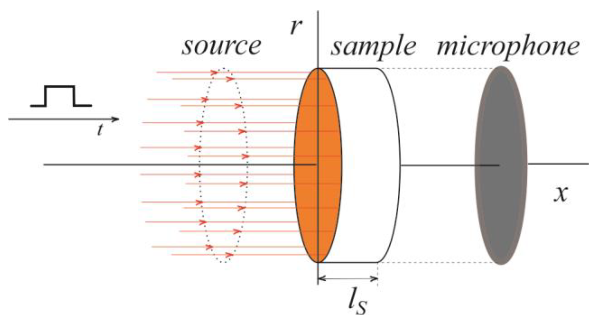
Figure 2.
Equivalent transmission line for description of heat transfer problem based on classical Fourier heat conduction theory.
Figure 2.
Equivalent transmission line for description of heat transfer problem based on classical Fourier heat conduction theory.
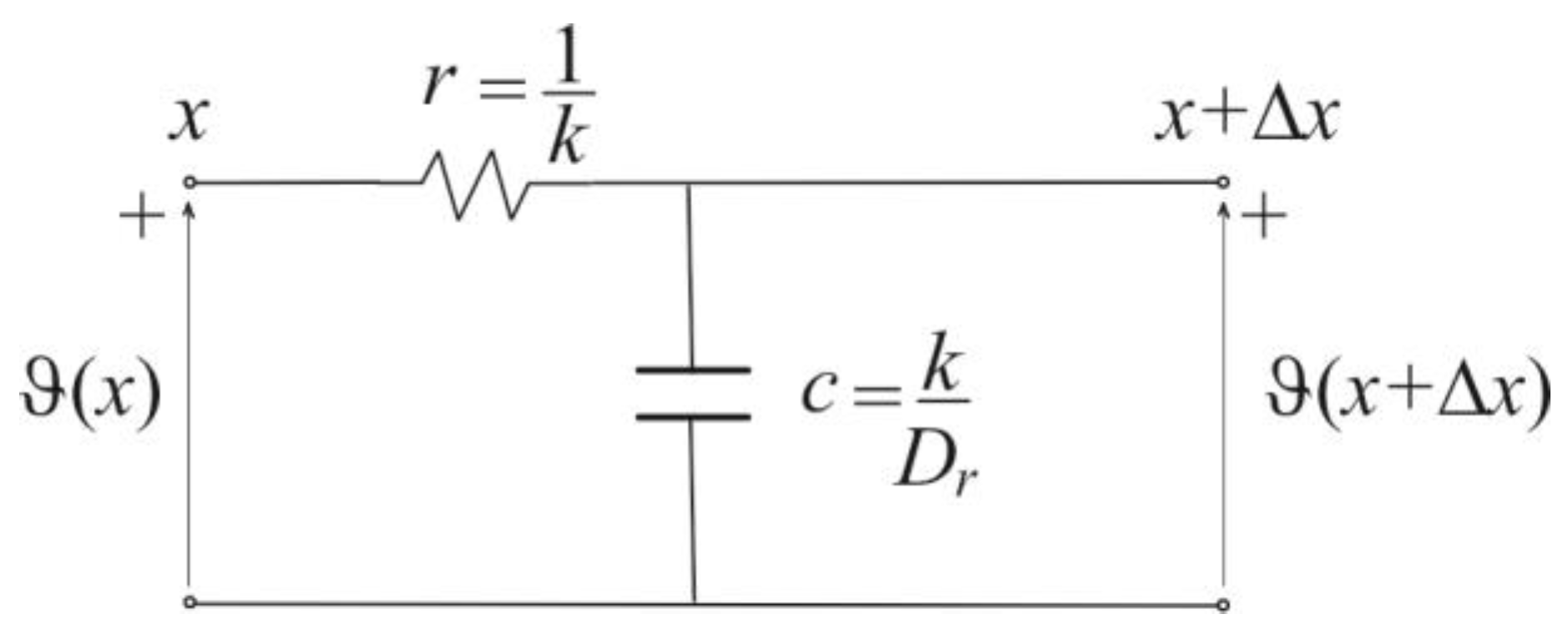
Figure 3.
The equivalent quadripole for calculation the surface temperature variations in semiconducting sample.
Figure 3.
The equivalent quadripole for calculation the surface temperature variations in semiconducting sample.
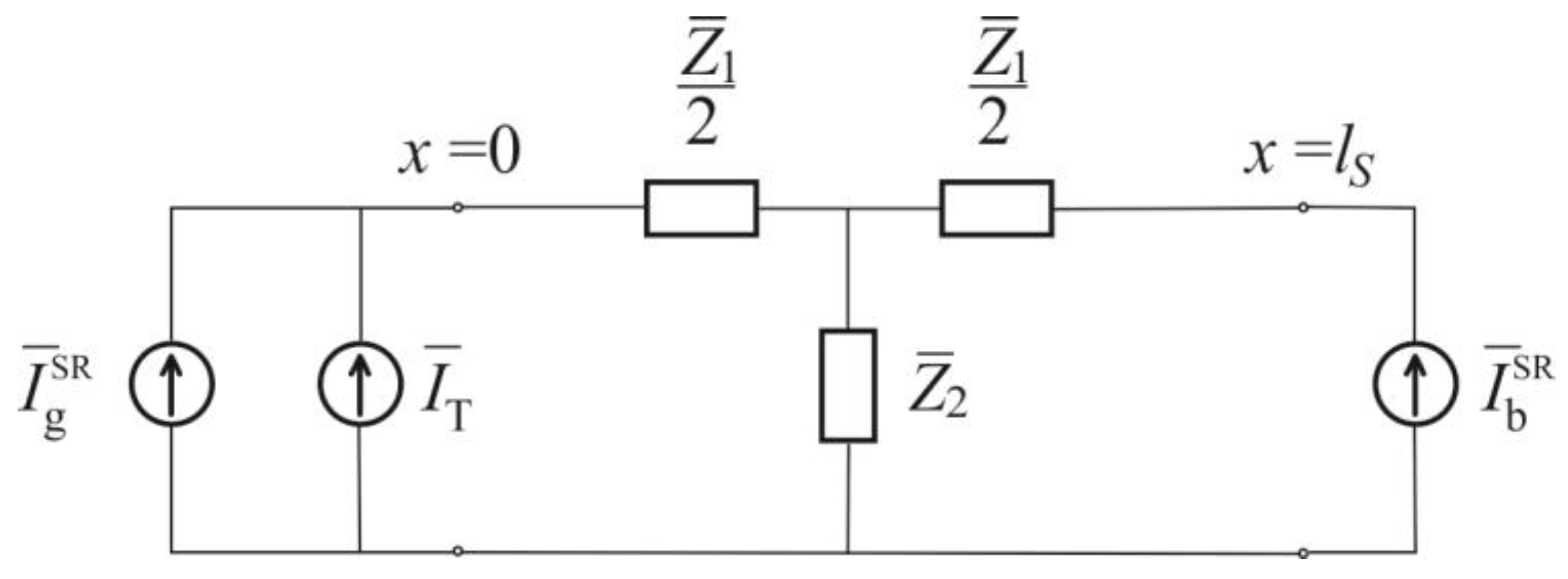
Figure 4.
Eqivalent electrical circuit for calculation of the temperature variations in thermally thin semiconducting sample.
Figure 4.
Eqivalent electrical circuit for calculation of the temperature variations in thermally thin semiconducting sample.
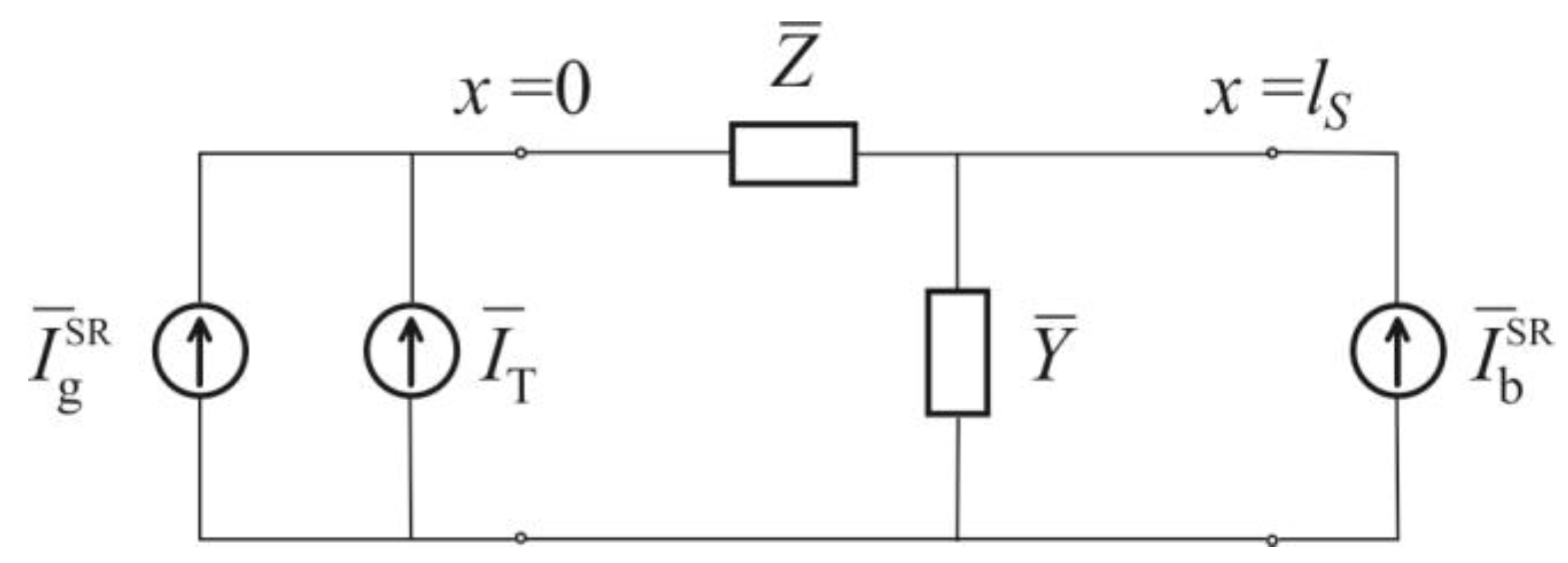
Figure 5.
The normalized time-domain temperature signal for a thermally thin and plasma opaque n-doped silicon sample. The red line represents the signal resulting from lattice thermalization (fast heat source), while the blue lines indicate the signal from surface recombinations at different sg values. The green lines represent the total signal caused by both sources: sg=6m/s (solid line), sg=10 m/s (dashed line), and sg=14m/s (dash-dotted line).
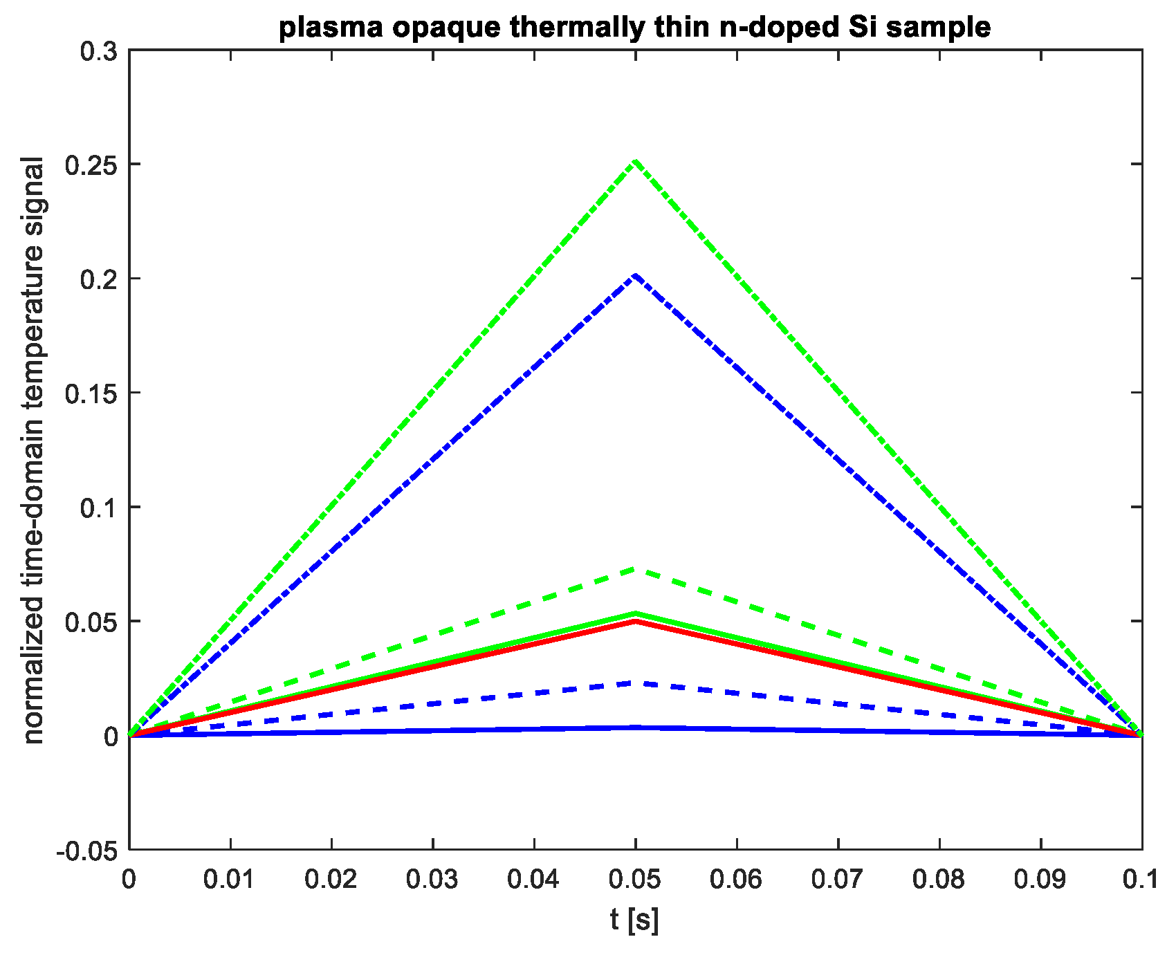
Figure 6.
The normalized time-domain temperature signal for a thermally thin and plasma opaque p-doped silicon sample. The red line represents the signal resulting from lattice thermalization (fast heat source), while the blue lines indicate the signal from surface recombinations at different sg values. The green lines represent the total signal caused by both sources: sg=6m/s (solid line), sg=10 m/s (dashed line), and sg=14m/s (dash-dotted line).
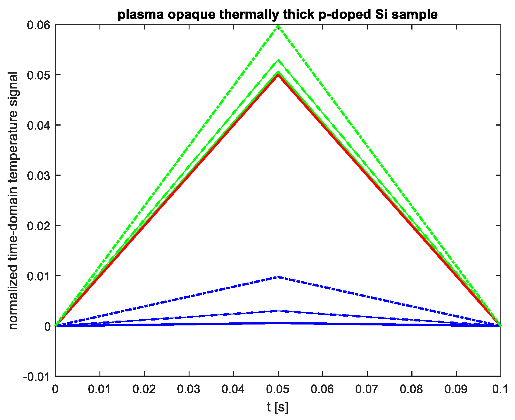
Figure 7.
The normalized time-domain temperature signal for a thermally thin and plasma-transparent n-doped silicon sample (ls=20µm, Dp=1.2×10⁻³ m2/s). The red line represents the signal originating from the thermalization of the lattice (a fast heat source), while the blue lines depict the signal resulting from surface recombinations for sb=6 m/s and various sg values. The green lines illustrate the total signal produced by both sources, with sg=6m/s represented by a solid line and sg=14m/s by a dashed line.
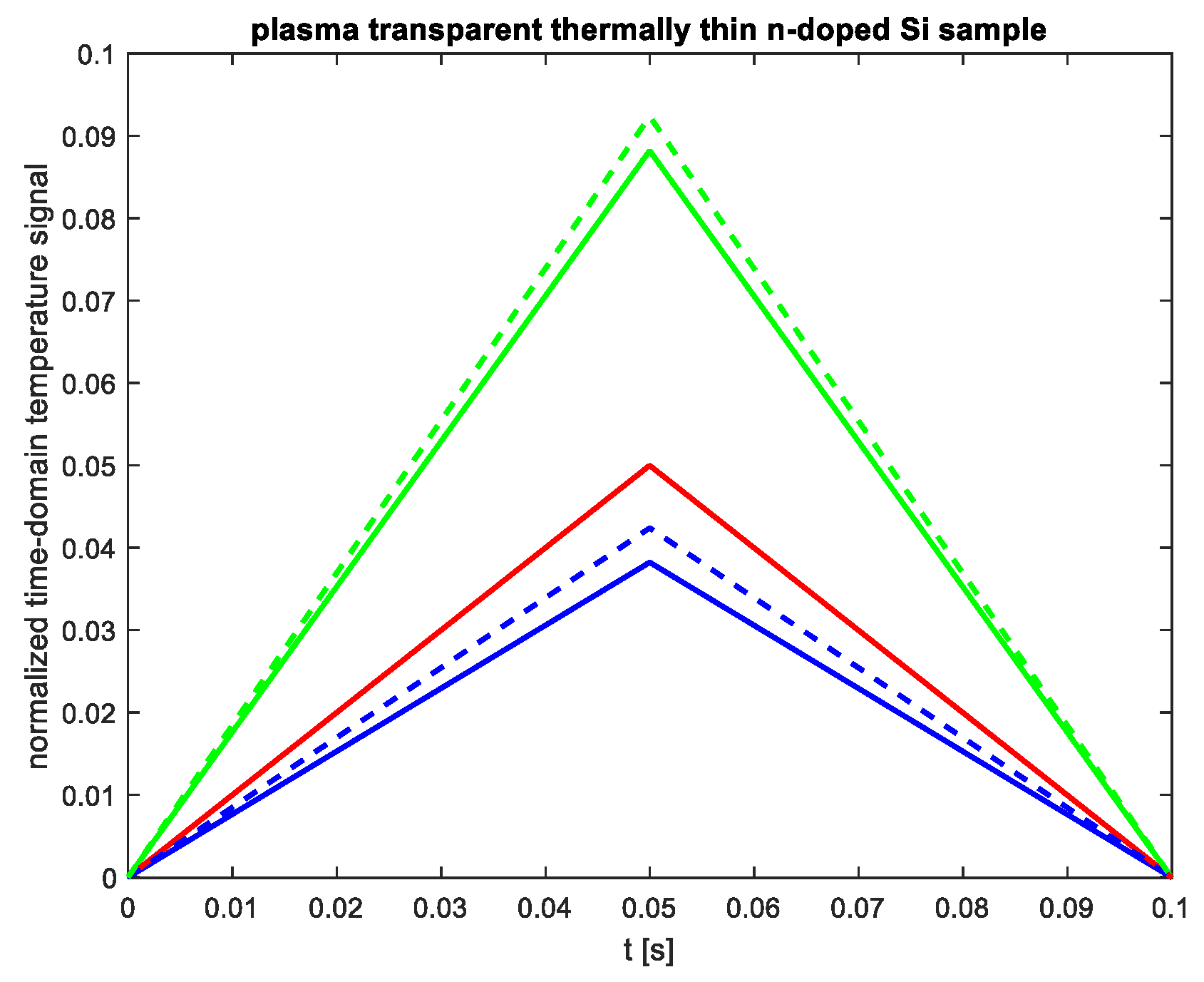
Figure 8.
The normalized time-domain temperature signal for a thermally thin and plasma-transparent n-doped silicon sample (ls=20 µm, Dp=1.2×10⁻³ m2/s). The red line represents the signal originating from the thermalization of the reset (a fast heat source), while the blue lines show the signal from surface recombinations for sg=2 m/s at different sb values. The green lines depict the total signal caused by both sources, with sb=6m/s indicated by a solid line and sb=24m/s by a dashed line.
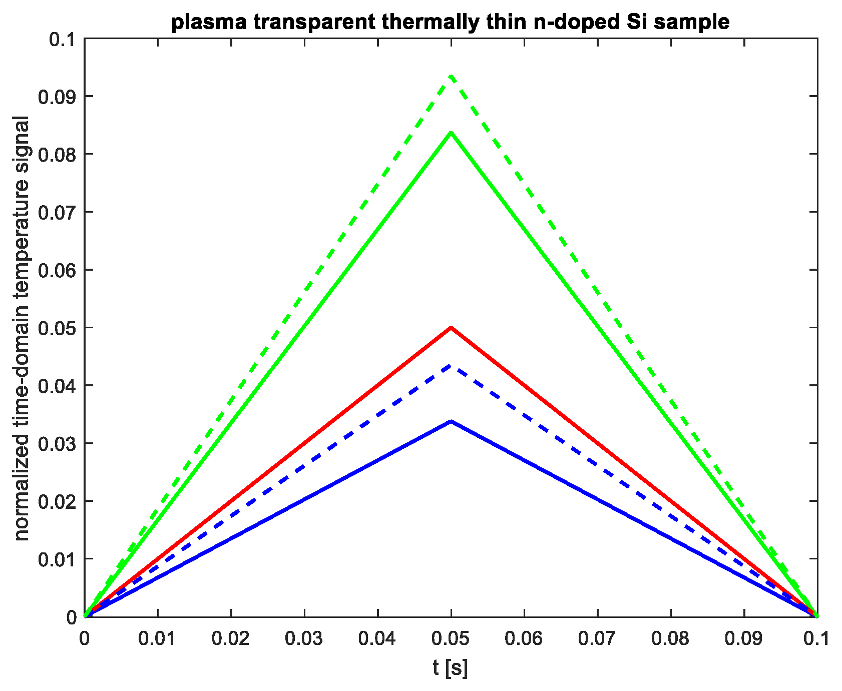
Figure 9.
The normalized time-domain temperature signal for a thermally thin and plasma-transparent p-doped silicon sample. The red line represents the signal originating from the thermalization of the lattice (a fast heat source), while the blue lines denote signals resulting from surface recombinations at various values of sg and sb. The green lines indicate the total signal contributed by both sources, with the solid line corresponding to sg=2 m/s and sb=2 m/s and the dashed line corresponding to sg=24 m/s and sb=24 m/s.
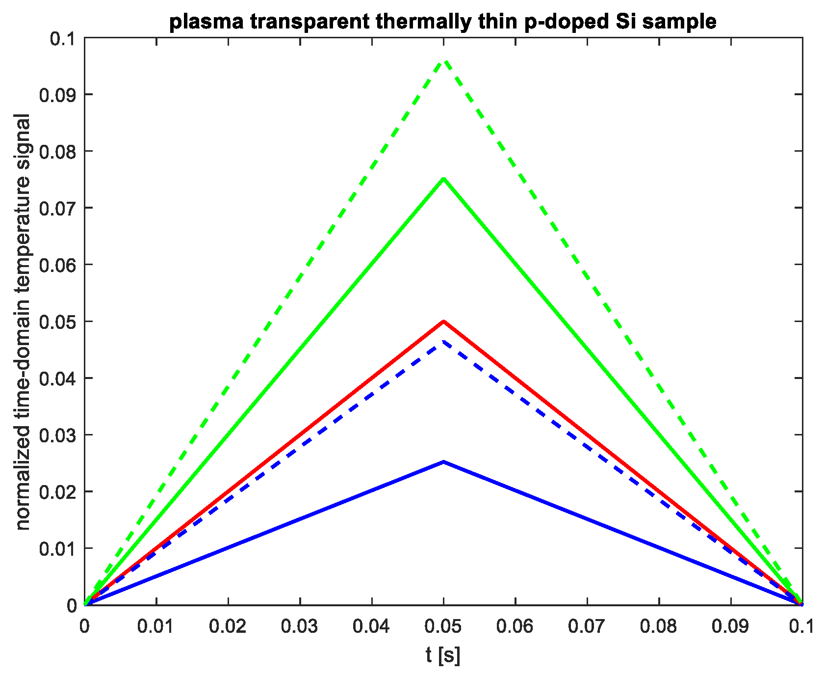
Table 1.
Electronic, thermal and geometrical properties of silicon samples used in analyzes of the model [12].
Table 1.
Electronic, thermal and geometrical properties of silicon samples used in analyzes of the model [12].
| Parameter | Value |
|---|---|
| Coefficient of diffusion of holes | 1.2·10-3 m2s −1 |
| Coefficient of diffusion of electrons | 3.6·10-3 m2s −1 |
| Lifetime of excess charge carriers | 5·10−6 s |
| Energy gap EG | 1.12 eV |
| The velocity of surface recombination | 2-24ms-1 |
| Coefficient of thermal difusivity | 9·10-5 m2s −1 |
| Thermal conductivity k | 150Wm-1K-1 |
Disclaimer/Publisher’s Note: The statements, opinions and data contained in all publications are solely those of the individual author(s) and contributor(s) and not of MDPI and/or the editor(s). MDPI and/or the editor(s) disclaim responsibility for any injury to people or property resulting from any ideas, methods, instructions or products referred to in the content. |
© 2025 by the authors. Licensee MDPI, Basel, Switzerland. This article is an open access article distributed under the terms and conditions of the Creative Commons Attribution (CC BY) license (http://creativecommons.org/licenses/by/4.0/).
Copyright: This open access article is published under a Creative Commons CC BY 4.0 license, which permit the free download, distribution, and reuse, provided that the author and preprint are cited in any reuse.


