
Submitted:
04 December 2024
Posted:
05 December 2024
You are already at the latest version
Abstract
When a sample of semiconducting material is illuminated by monochromatic light which photon energy is higher than the energy gap of the semiconductor, the part of absorbed electromagnetic energy is spent on the generation of pairs of excess carriers that are bound by Coulomb attraction. Photo-generated pairs diffuse through the material as a whole according to the density gradients established carrying the part of excitation energy through the semiconducting sample. This energy is indirectly transformed into heat where the excess negatively charged electron recombines with a positively charged hole and causes additional local heating of the lattice. In this paper, based on ambipolar diffusion partal differential equation in approximation of low-level injection, the spectral function of photoinduced charge carrier distribution was calculated and models of spectral functions of surface recombination heat sources were derived. By applying the inverse Laplace transform to derived models, the dynamics of recombination photoinduced heat sources at surfaces of semiconducting samples was studied for pulse optical excitations of very short and very long duration. It was shown that the photoexcited charge carriers could significantly affect semiconductor heating in dependence on pulse duration and velocity of surface recombinations, consequently influencing the performance of nanoelectronic and optoelectronic semiconductor devices.
Keywords:
transport of charge
; ambipolar diffusion
; low level injection
; recombination heat sources
; parabolic partial differential equation
; inverse Laplace transform
; irradiation function
1. Introduction
Semiconductors are materials where, due to strong ionic or covalent bonds between the structural elements of the crystal lattice, there is an energy gap between the valence and the conduction zone. The semiconductor is electroneutral as a whole, and the electronic and phononic subsystems are in a state of thermodynamic equilibrium when there is no external excitation, electric, magnetic, electromagnetic, or thermal [1].
When a sample of semiconducting materials is illuminated with photons of sufficient energy, the part of absorbed electromagnetic energy is directly transformed into heat via excitation of the crystal lattice oscillation, and the part of absorbed phonons excites the electrons from the valent to the conduction zone. At the place of excited electrons in the valence zone, the empty positively charged places, called holes, remain. The pairs of excess carriers are bound by Coulomb attraction and make up the plasma subsystem in a semiconducting sample. The plasma effect in semiconductors is used to develop numerous microelectronic, photodetector, and photovoltaic devices [1,2,3,4,5,6]. However, this effect also increases the semiconductor's internal energy and temperature. Consequently, it can cause a reduction in the operating temperature of semiconductor devices[2], the appearance of plasma elastic displacement in micromechanical sensors based on semiconductors[5,6], etc. Namely, the nonradiative deexcitation relaxation processes of both subsystems, phonon and plasma, influence temperature distribution across the illuminated semiconducting sample.
In several theoretical studies, the contribution of photo-generated plasma to the photothermal (PT) effect in semiconductors is completely ignored[7,8,9,10,11,12,13,14,15,16]. A priori neglecting the plasma effect in semiconductors is a very rough approximation, although there are circumstances in which it is applicable, e.g., in semiconductors with a wide energy gap[17], porous semiconductors[15,16], intrinsic and/or low doped semiconductors[7,8,9,10,11,12,13,14], or when using far infrared part of electromagnetic spectra, etc.
In general, there are two approaches to modeling the contributions of excess charge carriers to the PT effect in semiconductors that include electron-phonon interactions neglecting polaron effects [18,19,20]. Some studies consider semiconducting samples as complex systems consisting of phonon and electron subsystems and introduce two temperature models similar to laser-induced heat transfer models developed for metals [21,22,23,24,25]. The basic concept of these models is the following. When a laser pulse irradiates a material, the electrons are excited, absorbing the energy from the laser beam and increasing the temperature of the electron subsystem. Due to the difference in temperature of electron and phonon subsystems and the interaction between these subsystems, the lattice temperature increases until electrons and phonons reach thermal equilibrium states (at which electron and lattice reach the same temperature). In other words, the transmission energy from the electron subsystem to lattice vibration results from the temperature difference between the two subsystems and electron-phonon interactions. This approach can be beneficial for consideration of the photothermal effect in laser processing of semiconductors where laser beams of high power are used or in highly doped semiconductors, i.e., degenerated semiconductors in which the Fermi level is not in the forbidden gap[1,26].
The second approach to modeling the contribution of photo-generated carriers to the PT effect in semiconductors is the inclusion of the heat sources produced by bulk and surface recombinations of photo-generated excess charge carriers [27,28,29,30,31,32,33,34,35]. The basic assumption of such models is that the photo-generated charge carriers and the crystal lattice are at approximately the same temperature (there is no temperature difference between the plasma subsystem and the crystal lattice). The energy transfer from the photo-generated electron to the lattice results from Shockly-Read-Hall recombination of photoinduced electron-hole pairs and electron-phonon interactions [26]. This approach is suitable if the semiconductor is moderate doped and consequently non-degenerated (Fermi level is inside the energy gap) and there is low-power laser excitation [33].
In this paper, we develop the model of laser heating of semiconductors based on the second approach and study the evolution of recombination heat sources in a laser pulse-illuminated semiconducting sample to enable analyses of time-resolved photothermal (PT) signals and, consequently time domain PT characterization of electronic properties of semiconductors and semiconductor devices[36].
The structure of the paper is following. After this introduction section, Section 2 presents the ambipolar diffusion model of photo-generated charge carriers and its reduction to the transport of minority carriers in doped semiconductors under the condition of low-level injection. Based on this approximation, the model of the spectral function of heat sources created by the surface recombination of the photo-generated excess of charge carriers is derived. In Section 3, the evolution of these sources is calculated and analyzed in the case when the semiconductor is illuminated by a very short optical pulse or by a long optical pulse. The influence of the velocity of surface recombination and pulse duration on the size and time dependence of recombination heat sources are discussed. Finally, in Section 4, the most important conclusions were formulated.
2. Laser-Semiconductor Interaction and Spectral Functions of the Recombination Heat Sources
When a semiconductor sample is exposed to electromagnetic excitation, part of the excitation energy is absorbed, and part of the absorbed energy affects the oscillations of the lattice structural elements, directly converting them into heat [37]. This direct heat source there is in all substantial media not only in semiconductors and it will not be further considered in this paper.
If the wavelength of the optical excitation is such that the energy of the photon () is greater than the width of the energy gap of the semiconductor, part of the absorbed energy is spent on the photogeneration of quasi-free charge carriers. For all semiconductors with a narrow energy gap (), such as silicon (), this condition is met for all wavelengths from the visible part of the spectrum ().
The concentrations of photo-generated excess negative charge carriers (electrons) in the conduction zone and excess positive charge carriers (holes) in the valence zone follow the spatial distribution of the absorbed electromagnetic flux . The source of the charge carrier is proportional to the gradient of that flux and inversely proportional to photon energy [33,34,35]:
Since the absorbed electromagnetic flux depends on space coordinates, an inhomogeneous distribution of excess charge carriers appears along the illuminated semiconductor, which leads to the formation of a concentration gradient of both positive and negative charges and the directed transport of charges along the semiconductor sample from an area of higher to an area of lower concentration.
The mass of a quasi-free electron is different from the mass of a quasi-free hole[1], so the mobility of negatively and positively charged particles is different, due to which their spatial separation occurs. Because the electrons and holes are charged particles, any separation will induce an internal electric field between the two sets of charged particles. Still, the semiconductor as a whole is electroneutral. The negatively charged electrons and positively charged holes will then diffuse together with a single effective mobility and diffusion coefficient, and the electron-hole pairs coupled by Coulomb attraction will recombine together. This phenomenon where positively and negatively charged particles diffuse together due to interactions between them is called ambipolar diffusion[1].
Positively and negatively charged carriers, after some time, which is called the lifetime of the charge carriers, recombine in the volume and on the surfaces of the semiconductor, transferring their kinetic energy to the lattice. In this way, the excitation optical beam indirectly, through the recombination of photo-generated charge carriers, contributes to the heating of the lattice. These indirect heat sources are proportional to the concentration of photo-generated carriers and their recombination velocity.
During further theoretical consideration, we will consider the following assumptions:
1. The sample is illuminated uniformly over the entire surface (Figure 1), so a one-dimensional approximation can be introduced in further consideration
2. The sample is excited by a low power (smaller than 50 mW) amplitude-modulated optical beam, that is, by a time-dependent optical irradiance .
3. The optical absorption coefficient of the semiconductor is high, so all the light is absorbed in the thin layer of the semiconductor next to the illuminated surface, and the generation of excess charge carriers takes place on the illuminated surface of the sample[38].
According to the Beer-Lambert law, the absorbed flux of excitation energy is described by the expression:
Sources of photogeneration of carriers, based on Eq. (1), become:
Considering the high optical absorption coefficient, the surface source of photo-generated carriers is obtained:
where and symbol signify Dirac's delta function.
The above shows that assumption (3) is a reasonable approximation for semiconductors thicker than . For example, in the case of silicon, the optical absorption coefficient is of the order of [39,40], which means that light is absorbed in a thin layer, thick, which is already a layer ten times thinner than the thick sample and practically can be considered as a surface.
4. Indirect heat sources that appear due to the photogeneration of excess charge carriers and their volume and surface recombinations are proportional to the concentration of photo-generated excess charge carriers[33,34,35]:
where is the concentration of photoinduced excess charge carriers and is their lifetime. Experimental and theoretical investigations show that the recombination rate in the balk of the semiconducting sample is much less than that at sample surfaces [26,32,33,34,35,41,42,43]. Consequently, the contribution of volume recombinations to the heating of the sample is much smaller than the contribution of surface recombinations, so heat sources due to volume recombinations, Eq.5, will not be considered further.
As can be seen from Eqs.6 and 7, the dynamics of recombination heat sources depend on the dynamics of photo-generated excess charge carriers, so for the analysis of the evolution of recombination heat sources, it is necessary to solve the problem of distribution and evolution of photo-generated excess carriers in the semiconductor.
Due to the appearance of photo-generated charge carriers, electrons and holes, on the illuminated surface of the semiconductor, a concentration gradient is established along the sample, which is the cause of the diffusion of electrons and holes from the area of higher concentration to the area of lower concentration. Photo-generated pairs diffuse together due to Coulomb attraction between them. The equation of ambipolar diffusion (if an external electrical field is not applied) in one-dimensional approximation is given by the expression [1]:
where is a source of photo-generated carriers given by Eq.4, is a concentration of photo-generated charge carriers (excess charge carriers), is a lifetime of electrons and holes [1,44,45], and is the coefficient of ambipolar diffusion, given by [1]:
In Eq.9, symbols and denote the total electron concentration in the conduction zone and concentration of holes in the valent zone, respectively, where , , while and signify equilibrium concentrations of electrons and holes that depend on impurity concentrations [1].
Since is a function of and (Eq.9) and hence is a function of excess carrier concentrations (photo-generated charge carriers), Eq.9 is nonlinear. However, if the injected excess-carrier concentration is much smaller than the equilibrium majority-carrier concentration, i.e., for a p-doped semiconductor or for an n-doped semiconductor (it is the so-called low-level injection condition), the coefficient becomes equal to diffusion constant of minority carriers and Eq.8 becomes parabolic linear partial differential equation:
The distribution of photo-generated excess carriers in extrinsic semiconductors under low-level injection conditions can be described by the distribution of minority carriers.
It is important to note that quasi-free charge carriers cannot be found outside the illuminated sample, and surface recombinations define the flux of charged carriers (denoted with) at the boundary surfaces:
where and denote the velocity of surface recombination and depend on the method of processing the sample surfaces [33,36].
Considering Eq.4 and by integration of Eq.10 from point to (Figure 1), the problem of distribution of concentration of photo-generated carriers can be reduced to a system of homogeneous partial differential equations with inhomogeneous boundary conditions:
where Eq.14 is the mathematical representation of Fick's first low.
It is convenient to calculate surface concentrations of photo-generated carriers using a plasma-electrical analogy. Namely, Eq.13 is analog with the telegraph equation:
where inductance is equal to zero, and:
and , .
This means that the propagation of excess carrier concentration through a semiconductor can be represented by analogous voltage propagation through an electrical line without inductance, as shown in Figure 2.
By applying the Laplace transform on Eqs.13-16, the distribution of excess charge carriers can be described by the following homogeneous differential equations in the complex domain:
with inhomogeneous boundary conditions:
where:
represent analogs resistivity at ports of transmission line illustrated in Figure 2.
With is denoted the inverse coefficient of propagation:
and with characteristic impedance of transmission line:
With and are denoted the equivalent longitudinal impedance and admittance of transmission line:
And , , and are given by Eq.18.
It is interesting to note that the real part of the complex propagation coefficient is related to the weakening of the concentration and flux along the sample, i.e., to the diffusion length of the propagation of the disturbance in the concentration of charge carriers, and it is equal to:
In a steady state, the diffusion length of the excess charge carrier is maximal minimal and equal to .
With is denoted the Laplace transform of the time-dependent function, which describes the amplitude modulation of the excitation optical beam.
Using the plasma-electric analogy (Figure 2) and solving the system of ordinary differential equations Eqs.19-20 in the complex domain, the distribution of excess photo-generated carriers and their fluxes through the sample can be described by the concentration and flux of carriers on the non-illuminated side of the semiconductor:
Based on Eqs.28 and 29, the concentrations and fluxes on the sample surfaces are connected by a symmetric unimodular transfer matrix , the coefficients of which depend on the coefficient of propagation, impedance of transmission line (Eqs.24 and 25), and transmission line length and consequently on electronic properties of the photo-generated plasma and sample thickness:
where are:
Introducing new variables, total series impedance and total parallel admittance :
characteristic impedance, inverse coefficient of propagation, and matrix coefficients can be written in the following form:
Using the matrix representation Eq.31 and the boundary conditions given by Eqs. 21-22, the equivalent electrical circuit for calculating the surface concentrations of photo-generated carriers and surface fluxes is presented in Figure 3, with the impedances and given by the following expressions:
By solving a simple ladder network excited by a non-ideal current generator, shown in Figure 3, the equivalent impedance of the semiconductor and dependence of spectral function of the concentration of photo-generated charge carriers at an illuminated surface on excitation optical flux are calculated:
The spectral function of concentration on the non-illuminated side is calculated using matrix equation Eq.28, boundary condition Eq.22, and Eq.37:
By using definitions of recombination heat sources given by Eqs 6 and 7 and Eqs 38 and 39, the spectral functions of recombination heat sources at illuminated and non-illuminated surfaces of a semiconducting sample are calculated:
In the following, we consider two limiting cases: the case of a plasma opaque semiconductor (when the real part of the propagation coefficient Eq.27 is much smaller than the sample thickness) and the case of a plasma transparent sample (when the real part of the complex propagation coefficient Eq.27 is much larger than the thickness of the sample).
2.1. The case of plasma opaque semiconductor sample ( )
In the case of the plasma opaque semiconductor, the following approximation can be introduced:
Using Eq.35-37, the total equivalent impedance of the plasma opaque semiconductor is calculated:
Based on Eq.38 and 39 and Eq.43, the concentration of photo-generated carriers at sample surfaces are:
As can be concluded from Eq.45, the concentration of excess carriers at the non-illuminated surface in the plasma opaque sample is very small (), and consequently, the recombination heat sources at this surface can be neglected (Eq.7).
Based on Eq.6 and Eq.43, the recombination heat sources at illuminated surfaces of optically and plasma opaque semiconducting samples are derived:
2.2. The case of plasma transparent semiconductor sample ( )
If the semiconducting sample is plasma transparent so that the condition is fulfilled, then the following approximations can be introduced:
The coefficients of the transfer matrix , in that case, are reduced to:
so the circuit for calculating surface concentrations and fluxes illustrated in Figure 3 is reduced to the circuit shown in Figure 4.
Based on the circuit shown in Figure 4, the equivalent impedance of the plasma transparent can be calculated:
The concentrations of photo-generated carriers at the surfaces of the sample are obtained by using Eqs.38, 39, 47, 50, and 51:
By substituting Eq.52 in Eq.6 and Eq.3 in Eq.7, the models of spectral functions of recombination heat sources for optically opaque and plasma transparent samples are obtained:
3. Evolution of Recombination Photothermal Sources Generated by an Optical Pulse
In this section, we consider the evolution of photo-generated heat sources in a semiconductor when the sample is excited by a very short pulse that can be described by unity -pulse:
and if the sample is excited by a very long pulse described by the unity step function:
with is denoted the Heaviside's step function.
By replacing Eqs.58, 59 in Eq.46, and Eqs.54 and 55 and by finding the inverse Laplace transform, the expressions that describe the evolution of heat sources due to surface recombination in optically opaque semiconductor samples excited by an optical pulse for the two observed cases, the case of plasma opaque and the case of plasma transparent samples, are obtained.
3.1. Evolution of Recombination Heat Sources for Plasma Opaque Semiconducting Sample Excited by Optical Pulse
To find the inverse Laplace transform and to mathematically describe the evolution of heat sources in an optically and plasma opaque sample when it is excited by a short optical pulse, it is convenient to replace the defining expressions for total series impedance and total parallel admittance, Eq.33 in Eq.46. In that case, the spectral function described by Eq.46, taking into account the optical excitation spectral function given by Eq.58, becomes:
The spectral function of recombination heat sources at the illuminated surface of plasma opaque sample excited by the long optical pulse is obtained by replacing Eq 59 in Eq.46 and by using the defining expressions for total series impedance and total parallel admittance (Eq.33):
where the parameters , are related to the electronic properties of the semiconductor and its thickness by the following relations (obtained based on Eqs.18, 26, 30, and 33):
The inverse Laplace transform of Eqs 60-61 was found using the known solutions for the irrational function and function with irrational exponent given in Table 1, [47], and the known properties of inverse Laplace transform [46]:
The evolution of recombination heat source excited by a short optical pulse for an optically opaque and plasma opaque semiconductor sample is calculated by finding the inverse Laplace transform of Eq 60:
The evolution of recombination heat source excited by a long optical pulse for an optically opaque and plasma opaque semiconductor sample is calculated by finding the inverse Laplace transform of Eq 61:
where , .
3.2. Evolution of Recombination Heat Sources for Plasma Transparent Semiconducting Sample Excited by Optical Pulse
To find the inverse Laplace transform and mathematically describe the evolution of heat sources in an optically opaque and plasma transparent sample when excited by a short or long optical pulse, it is convenient to replace the defining expressions for total series impedance and total parallel admittance, Eq.33 in Eqs.54 and 55:
In the case of a long optical pulse, the spectral functions described by Eqs.54 and 55, taking into account the excitation spectral function Eq.59, become:
where parameters , , and based on Eqs.12,20,23, and 30 can be expressed via electronic properties and sample thickness:
By applying the method of partial fractions [46] to Eqs.69 and 70, the evolution of recombination sources in an optically opaque and plasma-transparent semiconductor sample excited by a short optical pulse is obtained:
By applying the method of partial fractions [46] to Eqs.71 and 72, the evolution of recombination sources in an optically opaque and plasma-transparent semiconductor sample excited by a long optical pulse is obtained:
4. Analysis and Discussion
Using the models described by Eqs.67-68 and 77-80 with parameters given by Eqs.62, 63, and 77-80, as well as the electronic parameters of silicon given in Table 2 [1,33], the evolution of recombination heat sources in optically opaque n-doped silicon samples () was analyzed for two thickness: and . In the first case, the semiconductor sample is plasma opaque, while in the second case, the sample is plasma transparent. It was considered that an optical pulse performs the excitation. In addition, it was considered that the sample is disk shape of a radius of 4 mm, uniformly illuminated by a uniaxial light beam (Figure 1) originating from a red laser diode (, photon energy) with the power of , so that the conditions for photogeneration ()without hot electrons are met (electronic and phonon subsystems are on same temperature).
To discuss the contribution of photo-generated charge carrier to the heating of semiconducting samples illuminated by monochromatic laser pulses, we analyze the following properties of recombination heat sources: maximum intensity, steady value of intensity, time required to reach a steady value of intensity, so-called settling time, and rate of change of intensity.
Figure 5 shows the time dependence of heat sources generated by recombination of photo-generated charge carriers on the surfaces of an optically opaque semiconductor sample for the case of plasma opaque () (Figure 5a,b) and for the case of plasma transparent sample () (Figure 5c-f). It was considered that the surface recombination velocity on the illuminated side is 2 m/s, while the surface recombination speed on the non-illuminated side is 24 m/s. In addition, the intensity of the heat sources was normalized to the product of the intensity of the excitation optical irradiance and the ratio of bandgap energy and phonon energy.
When there is a short excitation optical pulse, it creates a short-term concentration disturbance, regardless of whether it is a plasma-transparent or plasma-opaque sample, and generates a large amount of charge carriers in the initial moment, causing maximum intensity heat source at the illuminated surface, which after some time interval of the order of -(see Figs. 5a,c,e) recombine on the surfaces of the semiconductor and in bulk, so that the steady intensity of heat sources is equal to zero. Consequently, they can no longer affect the temperature of the semiconductor, see Figure 5a,c,e. The settling time linearly depends on the thickness of the semiconducting sample. In ten times thicker plasma opaque samples, this time constant is ten times larger than in plasma transparent samples (compare Figure 5a with Figure 5c,e).
In plasma opaque samples, the maximum concentration of carriers reached at the initial moment on the illuminated surface forms a heat source whose intensity is four orders of magnitude higher than the product of excitation optical irradiance and ratio of energy gap and photon energy. Still, its evolution is exponentially decreasing in time, with a rate of decrease that depends on the ratio of the square of recombination velocity on the illuminated surface and the diffusion coefficient of minority carriers in the semiconductor, as well as on the inverse lifetime of excess carriers (Eqs.63 and 67), Figure 5a.
The intensity of the heat sources on the illuminated side of the plasma opaque semiconductor sample is lower than the intensity of the heat sources on the front side of the plasma transparent sample when they are excited by a short pulse (Figure 5a,c), with all other sample parameters being the same, since in plasma opaque samples there is the influence of volume recombinations that reduce the maximum value of the concentration of excess charge that can appear in the semiconductor, thus affecting the maximum intensity of recombination heat sources on the illuminated side.
The intensity of heat sources on the non-illuminated side of the plasma transparent sample is higher than the intensity of heat sources on the illuminated side (Figure 5c,e) when the sample is excited by a short pulse, although the concentration of carriers decreases along the sample and is highest on the illuminated side.
When a semiconducting sample is excited by a long pulse, recombination heat sources have no maximum intensity. For that excitation, the intensity of heat sources increases after the rising edge of the optical pulse up to steady values in both plasma transparent and plasma opaque samples (Figure 5b,d,f). The settling time of these sources (the time for which they reach their steady value) is related to the parameters and in the plasma opaque sample (Eqs.62 and 63, Figure 5b)), while the settling time in plasma transparent samples is related to parameter ,, and (Eqs.73-76, Figs.5d,f)) and consequently depends on the lifetime of the photo-generated charge carriers, velocity of surface recombinations and diffusion length of excess charge carriers. The settling time in plasma transparent samples is shorter than the settling time in plasma opaque samples, and it linearly depends on the thickness of the sample, which is similar to the case of short pulse excitation.
The steady intensity of the recombination heat source on the illuminated side of the plasma opaque sample is several times larger than the corresponding intensity of the plasma transparent sample when these samples are excited by a long optical pulse (Figs.5b,d), unlike to the case of short pulse excitation (Figs.5a,c), due to surface recombinations at non-illuminated side significantly decrease the concentration of excess charge carriers in plasma transparent samples (Figure 4) in steady state.
Interestingly, the steady intensities of the heat sources are much smaller than the product of excitation optical irradiance and the ratio of energy gap and photon energy if the sample is excited with a long pulse (Figure 5b,d, and f). In addition, even though the case was considered when the velocity of surface recombination is higher on the non-illuminated side of the plasma transparent sample, in the case of excitation with a long pulse, sources of lower intensity appear on this surface than on the illuminated side, following the distribution of excess carrier concentration. (Figs.5f,d).
In general, it can be considered that the evolution of recombination heat sources follows the excitation optical pulse if the processes are observed on a scale of the order of milliseconds to, which corresponds to the observation and detection of thermal processes.
Figure 6 shows recombination heat sources generated by short and long optical pulses on the illuminated side of the sample for several values of surface recombination velocity.
As can be seen from Figure 6a, for short pulse excitation, the settling time and maximum intensity of heat sources increase if the velocity of surface recombinations at the illuminated side increases, but the time dependence of the recombination heat source generated by a very short optical pulse is not changed, especially on a time-scale of heat conduction processes. Similarly, if increases then the settling time and steady value of the intensity of heat sources increase for the semiconducting sample excited by a very long optical pulse (Figure 6b). All steady intensity values are lower than the product of optical irradiance and the ratio of energy gap and photon energy (Figure 6b).
Figure 7 shows the recombination heat sources on the illuminated and non-illuminated sides of the plasma transparent sample excited by a short optical pulse for several combinations of and.
As can be seen from Figure 7, and affect the maximum intensity of recombination heat sources and their settling time if the plasma transparent sample is excited by a short pulse.
If increases and is constant, both quantities, maximum of the intensity of the recombination source on the illuminated surface and the settling time increase (Figure 7a, black and blue lines, and red and green lines). On the contrary, the increase of if is constant affects the decrease in intensity and settling time of heat sources at the illuminated surface (Figure 7a, red and black lines and green and blue lines). The maximum intensity can be obtained for a maximum of illuminated surface recombination velocity and minimum non-illuminated surface recombination velocity (green line, Figure 7a), while the maximum settling time can be obtained for a minimum of both and (red line, Figure 7a).
If increases and is constant, the intensity of heat sources at the non-illuminated surface of the plasma opaque semiconducting sample increases. However, the settling time of these sources decreases (Figure 7b, red and black lines, and green and blue lines). The influence of increasing if is constant is entirely different. If increases and is constant, the intensity of heat sources at the non-illuminated surface of the plasma opaque semiconducting sample decreases, while the settling time of these sources increases (Figure 7b, black and blue lines, and red and green lines). The maximum intensity can be obtained for the maximum of the non-illuminated surface recombination velocity and minimum illuminated surface recombination velocity (black line, Figure 7b). In contrast, the maximum settling time can be obtained for the minimum of both and (red line, Figure 7b).
Figure 8 shows the evolution of recombination heat sources on the illuminated and non-illuminated sides of the plasma transparent semiconductor sample excited by a very long optical pulse for several combinations of and .
As can be seen from Figure 8, changes in and affect the steady value and the settling time of recombination heat sources excited by long optical pulse. The maximum steady intensity at the illuminated surface of a semiconducting sample excited by very long optical pulse can be obtained for a maximum of the illuminated surface recombination velocity and a minimum of the non-illuminated surface recombination velocity (green line, Figure 8a), while the maximum settling time can be obtained for the minimum of both and (red line, Figure 8a).
The maximum steady intensity at non-illuminated surface of a semiconducting sample excited by very long optical pulse can be obtained if both surface recombination velocities are maximal (blue line, Figure 8b), while the maximum settling time can be obtained for a minimum of both and (red line, Figure 8b).
5. Conclusion
In the paper, a model of recombination heat sources generated by illuminating semiconductors with pulses of different lengths was developed. The model is based on the ambipolar diffusion model of the photo-generated excess of charge carriers and the approximation of low-level injection.
The time dependence of recombination heat sources in plasma-opaque and plasma-transparent semiconductor samples mostly depends on the length of the optical pulse excitation. For short pulse optical excitation, recombination heat sources have a maximal value in the initial moment that is a few orders of magnitude higher than a product of optical irradiance and the ratio of energy gap and exciting photon energy. During the time interval called settling time, the intensity of these sources becomes approximately equal to zero. For long pulse excitation, the intensity of recombination heat sources in the initial moment equals zero and increases with time, reaching a steady value after settling time.
The maximum intensity, the steady value, and the settling time of recombination heat sources generated by pulse optical depend on the thickness of the sample and velocities of surface recombinations at both surfaces of the illuminated semiconducting sample.
The time dependence of the recombination heat sources, on a time scale greater than 100 microseconds, closely follows the time dependence of the optical excitation in both plasma-opaque and plasma-transparent semiconductor samples. For short excitation optical pulses described by the delta function, the evolution of the recombination heat sources can also be approximately described by the delta function. In contrast, for long optical pulses described by the step function, the evolution of the recombination heat sources can be described by the delayed step function.
The presented results show that recombination heat sources can significantly affect the temperature distribution inside a semiconductor sample illuminated by optical pulses, which will be the subject of our further research.
Author Contributions
All authors contributed to this work. S.G; methodology, S.G.,M.D.,; software, S.G.; validation, S.G,. M.D.,K.Dj., D.M.,and E.S.; formal analysis, S.G., M.D., K.Dj., D.M., and E.S.; investigation, S.G., M.D., K.Dj., D.M., and E.S.; resources, E.S.; data curation, D.M; writing—original draft preparation, S.G., K.Dj., D.M; writing—review and editing, S.G., K.Dj., D.M; visualization, S.G., K.Dj., D.M; supervision, E.S, M.D.; project administration, D.M.; funding acquisition, E.S.
Declaration of competing interest: The authors have no conflicts to disclose.
Data Availability: This study did not generate any datasets.
Acknowledgments
This work was financially supported by the Ministry of Science, Technological Development, and Innovation of the Republic of Serbia (Contract No. 451–03–66/2024–03/200017).
References
- Wang, S. Fundamentals of Semiconductor Theory and Device Physics. (Prentice Hall, Inc. 1989). ISBN 0-13-344425-2.
- Sze, S. M. Physics of Semiconductor Devices. 2nd edn, (John Wiley and Sons, 1981). ISBN:9780471143239.
- Würfel, P. Physics of Solar Cells: From Basic Principles to Advanced Concepts. (Wiley, 2009). ISBN: 978-3-527-40857-3.
- Butler-Caddle, E.; Jayawardena, K. D. G. I.; Wijesekara, A.; Milot, R. L.; Lloyd-Hughes, J. Distinguishing carrier transport and interfacial recombination at perovskite/transport-layer interfaces using ultrafast spectroscopy and numerical simulation. Phys. Rev. Appl. 22, 024013 (2024). [CrossRef]
- Todorovic, D. M., Cretin, B., Song, Y. Q. & Vairac, P. Photothermal elastic vibration method: Investigation of the micro-electro-mechanical-systems. J Phys Conf Ser 214, 012105 (2010). [CrossRef]
- Benjamin Cyr, V. S., Yan Long et al. How Lasers Exploit Photoacoustic and Photoelectric Phenomena to Inject Signals into MEMS Microphones, 2024 . [CrossRef]
- Bychto, L.; Maliński , M.; Chrobak, Ł.; Zakrzewski, J.; Boumhamdi, M.; Investigations of optical and thermal properties of surface layers of Cd1−xBexTe samples by the photoacoustic method. OPTO-ELECTRON REV 32, e150186 (2024). [CrossRef]
- Zakrzewski, J.; Maliński, M.; Bachiri, A.; Strzałkowski, K. Photothermal determination of the optical and thermal parameters of CdxZn1-xSe mixed crystals. J. mater. sci. eng., B 271, 115305 (2021). [CrossRef]
- Fournier, D., Boccara, C., Skumanich, A. & Amer, N. M. Photothermal investigation of transport in semiconductors: Theory and experiment. Journal of Applied Physics 59, 787-795 (1986). [CrossRef]
- Forget, B. C. & Fournier, D. in Semiconductors and Electronic Materials (eds A. Mandelis & P. Hess) Ch. 7, (SPIE Opt. Eng. Press, 2000).
- Stanimirović, Z., Stanimirović, I., Galović, S., Djordjević, K. & Suljovrujić, E. Transmission pulse photoacoustic response of thin semiconductor plate. Journal of Applied Physics 133 (2023). [CrossRef]
- Galovic, S. P. et al. Time-domain minimum-volume cell photoacoustic of thin semiconductor layer. I. Theory. Journal of Applied Physics 133 (2023). [CrossRef]
- Popović, A., Šoškić, Z., Stojanović, Z., Čevizović, D. & Galović, S. On the applicability of the effective medium approximation to the photoacoustic response of multilayered structures. Phys. Scr. 2012, 014066 (2012). [CrossRef]
- Bertolotti, M. et al. New photothermal deflection method for thermal diffusivity measurement of semiconductor wafers. Rev. Sci. Instrum. 68, 1521-1526 (1997). [CrossRef]
- Isaiev, M. et al. Thermal conductivity of meso-porous germanium. Applied Physics Letters 105 (2014). [CrossRef]
- Isaiev, M. et al. Thermal conductivity of partially amorphous porous silicon by photoacoustic technique. Mater. Lett. 128, 71-74 (2014). [CrossRef]
- Yoshikawa, A., Matsunami, H. & Nanishi, Y. in Wide Bandgap Semiconductors: Fundamental Properties and Modern Photonic and Electronic Devices (eds Kiyoshi Takahashi, Akihiko Yoshikawa, & Adarsh Sandhu) 1-24 (Springer Berlin Heidelberg, 2007).
- Čevizović, D., Zeković, S. & Ivić, Z. The influence of polaron–phonon interaction on absorption spectra in molecular crystals. Chem. Phys. Lett. 480, 75-81 (2009). [CrossRef]
- Čevizović, D., Galović, S., Zeković, S. & Ivić, Z. Boundary between coherent and noncoherent small polaron motion: Influence of the phonon hardening. Physica B: Condensed Matter 404, 270-274 (2009). [CrossRef]
- Čevizović, D., Ivić, Z., Toprek, D., Kapor, D. & Pržulj, Ž. The influence of the interchain coupling on large acoustic polarons in coupled molecular chains: Three coplanar parallel molecular chains. Chaos Solit. Fractals. 73, 71-79 (2015). [CrossRef]
- Sobolev, S. L. Nonlocal two-temperature model: Application to heat transport in metals irradiated by ultrashort laser pulses. Int. J. Heat Mass Transfer 94, 138-144 (2016). [CrossRef]
- Mozafarifard, M., Liao, Y., Nian, Q. & Wang, Y. Two-temperature time-fractional model for electron-phonon coupled interfacial thermal transport. Int. J. Heat Mass Transfer 202, 123759 (2023). [CrossRef]
- Lashkevych, I., Titov, O. & Gurevich, Y. G. Recombination and temperature distribution in semiconductors. Semicond. Sci. Technol. 27, 055014 (2012). [CrossRef]
- Titov, O. Y. & Gurevich, Y. G. Temperature gradient and transport of heat and charge in a semiconductor structure. Low Temperature Physics 47, 550-554 (2021). [CrossRef]
- Kamel, A., Lotfy, K. & El-Bary, A. Plasma-thermal-elastic waves of semiconductor induced by laser pulses with hydrostatic initial stress and the hyperbolic two-temperature theory. Waves in Random and Complex Media, 1-19 . [CrossRef]
- Cui, X., Ruan, Q., Zhuo, X., Xia, X., Hu, J., Fu, R., Li, R., Wang,J., Xu, H. Photothermal Nanomaterials: A Powerful Light-to-Heat Converter, Chem. Rev. 2023, 123(11) 6891−6952, . [CrossRef]
- Gärtner, W. W. Photothermal Effect in Semiconductors. Phys. Rev. 122, 419-424 (1961). [CrossRef]
- Todorović, D. M. Plasma, thermal, and elastic waves in semiconductors. Rev. Sci. Instrum. 74, 582-585 (2003). [CrossRef]
- Miranda, L. C. M. Theory of the photoacoustic effect in semiconductors influence of carrier diffusion and recombination. Appl. Opt. 21, 2923-2928 (1982). [CrossRef]
- Isaiev, M., Kuryliuk, V., Kuzmich, A. & Burbelo, R. Photothermal Transformation In Heterogeneous Semiconductors Structures Under Its Pulse Laser Irradiation: Role Of Electron-Hole Diffusion. Archives of Metallurgy and Materials 58, 1351-1354 (2013). [CrossRef]
- Todorovic, D. & Nikolic, P. Investigation of carrier transport processes in semiconductors by the photoacoustic frequency transmission method. Optical Engineering 36, 432-445 (1997). [CrossRef]
- Song, P. et al. Surface recombination velocity on wet-cleaned silicon wafers using heterodyne lock-in ca rrierography imaging: measurement uniqueness investigation. Semicond. Sci. Technol. 35, 055013 (2020). [CrossRef]
- Todorovic, D. M. & Nikolic, P. M. in Semiconductors and Electronic Materials (eds A. Mandelis & P. Hess) Ch. 9, (SPIE Opt. Eng. Press, 2000).
- Rojas-Trigos, J. B., Calderón, A. & Marín, E. A practical model for the determination of transport parameters in semiconductors. J. Mater. Sci. 46, 7799-7805 (2011). [CrossRef]
- Mandelis, A. Laser infrared photothermal radiometry of semiconductors: principles and applications to solid state electronics. Solid•State Electron. 42, 1-15 (1998). [CrossRef]
- Djordjevic, K. L. et al. Transmission pulse photoacoustic set-up for characterization of solids. 21st International Symposium INFOTEH-JAHORINA (2022).
- Sablikov, V. A. & Sandomirskii, V. B. The Photoacoustic Effect in Semiconductors. physica status solidi (b) 120, 471-480 (1983). [CrossRef]
- Stanimirović, I., Markushev, D., Stanimirović, Z., Galović, S. & Djordjević, K. Analysis of plasma-elastic component of time-domain photoacoustic response. Journal of Applied Physics 133 (2023). [CrossRef]
- Adachi, S. The Handbook on Optical Constants of Semiconductors: In Tables and Figures. (World Scientific Publishing, 2012).
- Djordjevic, К. L. et al. Photoacoustic optical semiconductor characterization based on machine learning and reverse-back procedure. Optical and Quantum Electronics 52, 247 (2020). [CrossRef]
- Volovichev, I. N., Logvinov, G. N., Titov, O. Y. & Gurevich, Y. G. Recombination and lifetimes of charge carriers in semiconductors. Journal of Applied Physics 95, 4494-4496 (2004). [CrossRef]
- M. Pawlak; S. Pal; A. Ludwig; A. D. Wieck On the infrared absorption coefficient measurement of thick heavily Zn doped GaAs using spectrally resolved modulated photothermal infrared radiometry J. Appl. Phys. 122(13):135109 (2017) . [CrossRef]
- M. Pawlak, A. Panas, A. Ludwig, A.D. Wieck On measurement of the thermal diffusivity of moderate and heavily doped semiconductor samples using modulated photothermal infrared radiometry, Thermochimica Acta 650, 33-38 (2017) . [CrossRef]
- J. Zakrzewski; M. Pawlak; O. Matsuda; D. Todorovic; J. Liu, Semiconductor physics: Plasma, thermal, elastic, and acoustic phenomena , J. Appl. Phys. 136, 120401 (2024) . [CrossRef]
- Sun, Q., Melnikov, A., Wang, J. & Mandelis, A. Simultaneous determination of effective carrier lifetime and resistivity of Si wafers using the nonlinear nature of photocarrier radiometric signals. Journal of Physics D: Applied Physics 51, 15LT01 (2018). [CrossRef]
- Stojic, M. Continuous System of Automatic Control (in Serbian). (Naucna knjiga, 1991).
- Chen, Y. Q., Petras, I. & Vinagre, B. M. A list of Laplace and Inverse Laplace Transforms Related to Fractional Order Calculus. Available online: http://www.tuke.sk/petras/foc_laplace.pdf (2007).
Figure 1.
Geometry of the problem.
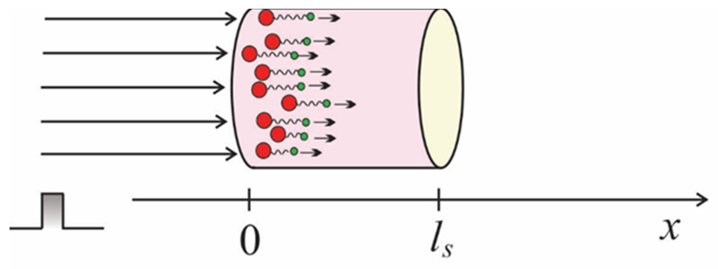
Figure 2.
Equivalent electrical representation of propagation of photoinduced excess charge carriers across the semiconducting sample.
Figure 2.
Equivalent electrical representation of propagation of photoinduced excess charge carriers across the semiconducting sample.
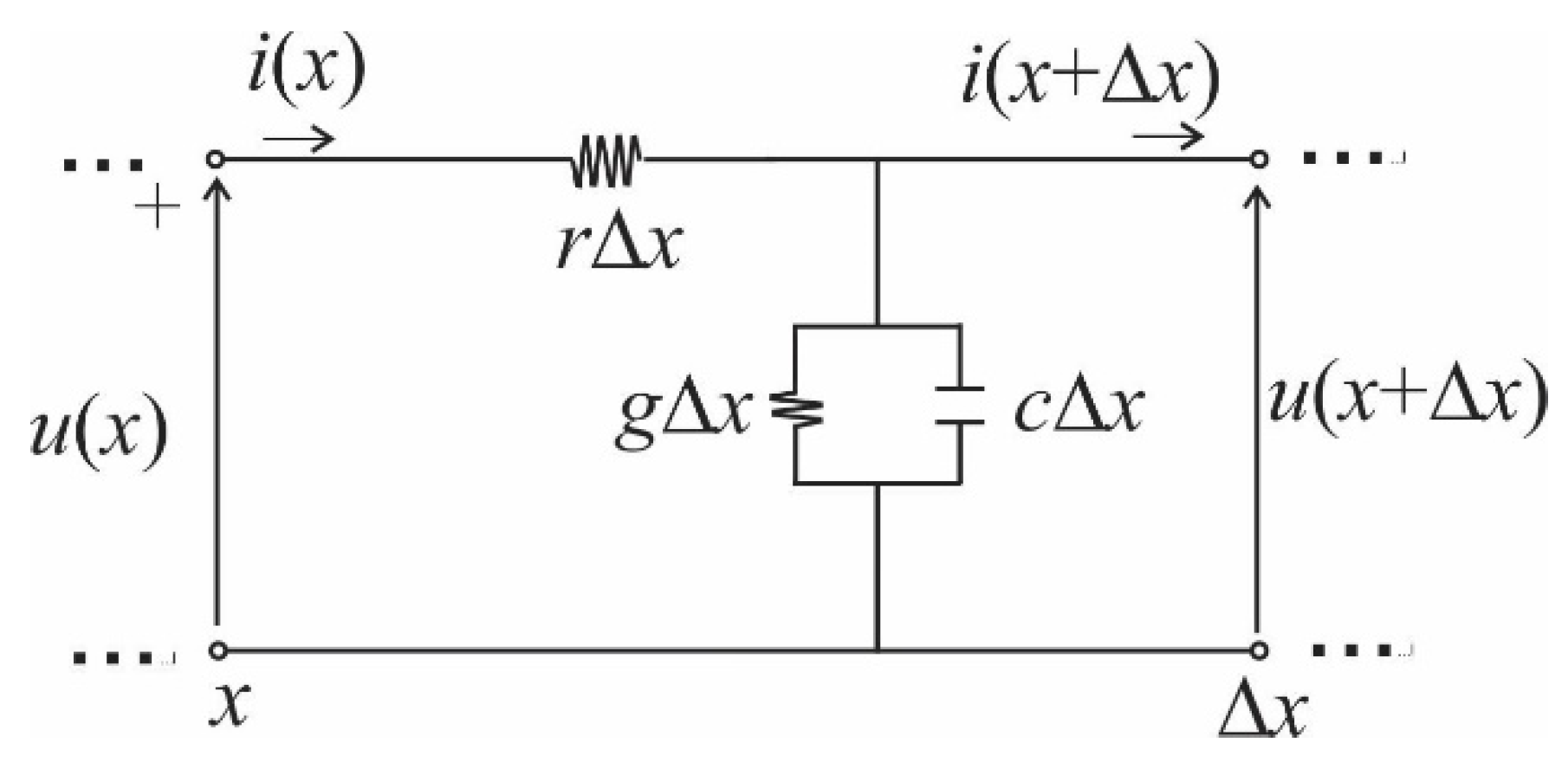
Figure 3.
Equivalent electrical network for calculating excess carrier concentrations at sample surfaces.
Figure 3.
Equivalent electrical network for calculating excess carrier concentrations at sample surfaces.
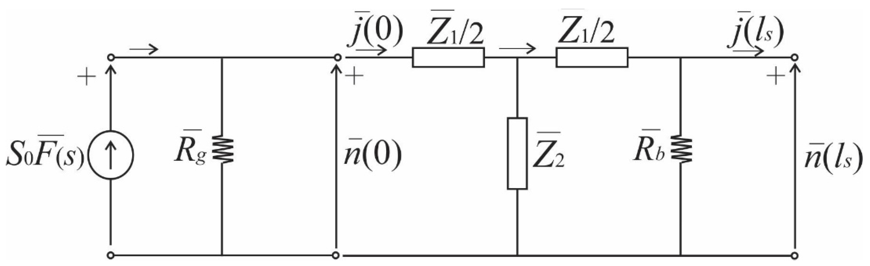
Figure 4.
Equivalent electrical circuit for calculation of surface concentrations of excess carriers in plasma transparent semiconducting sample.
Figure 4.
Equivalent electrical circuit for calculation of surface concentrations of excess carriers in plasma transparent semiconducting sample.
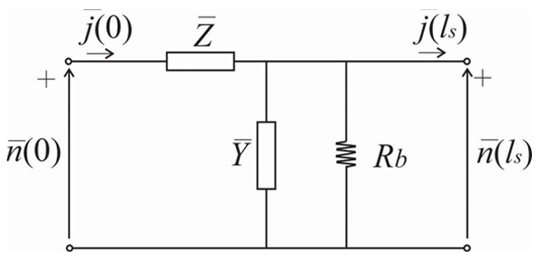
Figure 5.
Evolution of recombination heat sources in the semiconducting sample: at the illuminated surface of a) plasma opaque sample excited by a very short laser pulse; b) plasma opaque sample excited by very long laser pulse; c) plasma transparent sample excited by very short laser pulse; d) plasma transparent sample excited by very long laser pulse; at the non-illuminated surface of plasma transparent sample excited by e) very short laser pulse; f) very long laser pulse.
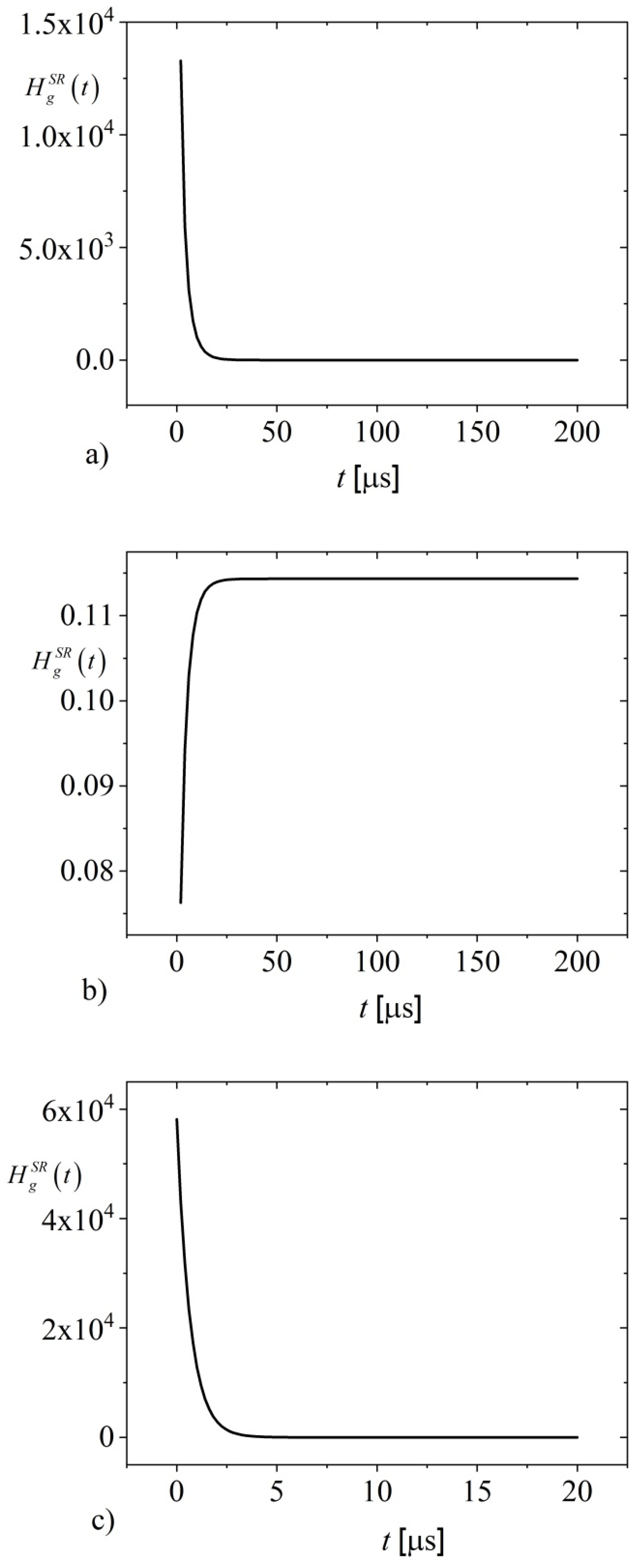
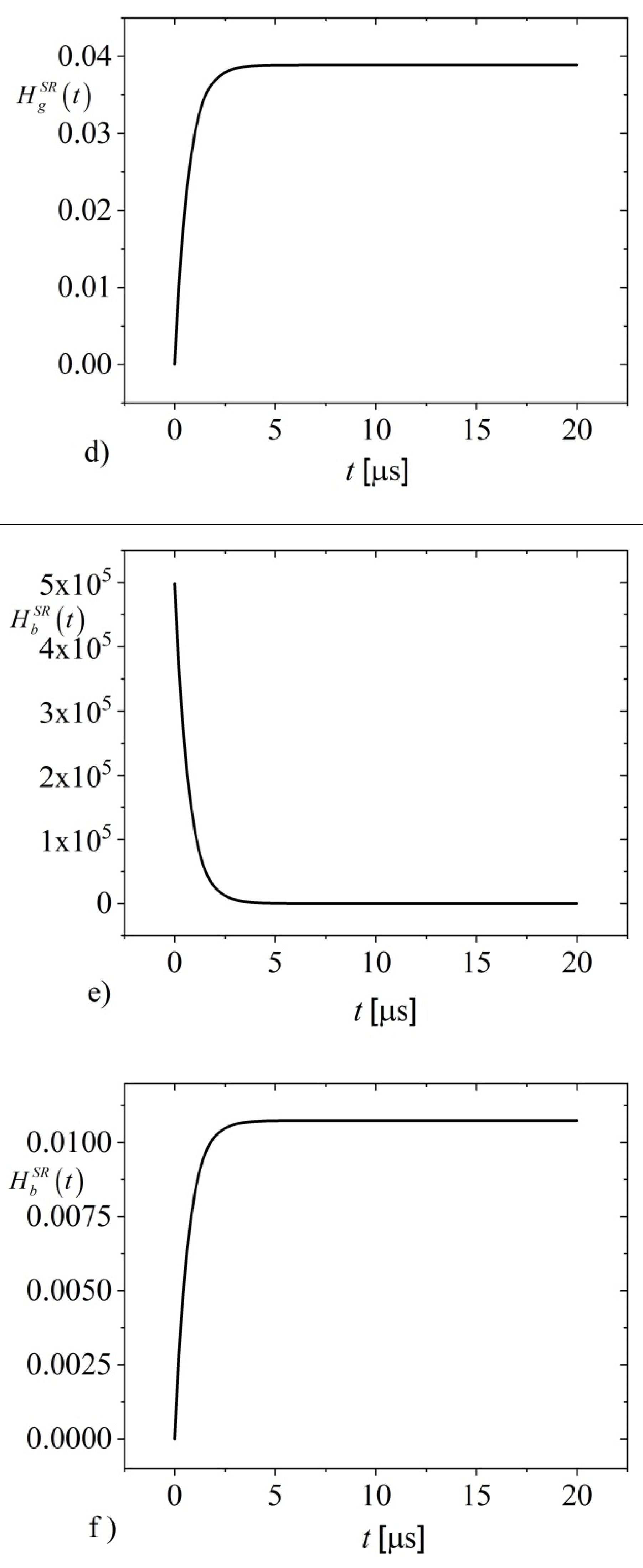
Figure 6.
Influence of on the evolution of heat sources in a plasma opaque semiconductor sample when it is excited by optical pulses of different lengths. Time dependence of the recombination heat source on the illuminated side of the sample when the sample is excited by: a) very short optical pulse; b) very long optical pulse.
Figure 7.
Influence of and on the evolution of heat sources in a plasma-transparent semiconductor sample upon its excitation by short optical pulses. Time dependence of the recombination heat source: a) on the illuminated side and b) on the non-illuminated side of the sample.
Figure 7.
Influence of and on the evolution of heat sources in a plasma-transparent semiconductor sample upon its excitation by short optical pulses. Time dependence of the recombination heat source: a) on the illuminated side and b) on the non-illuminated side of the sample.
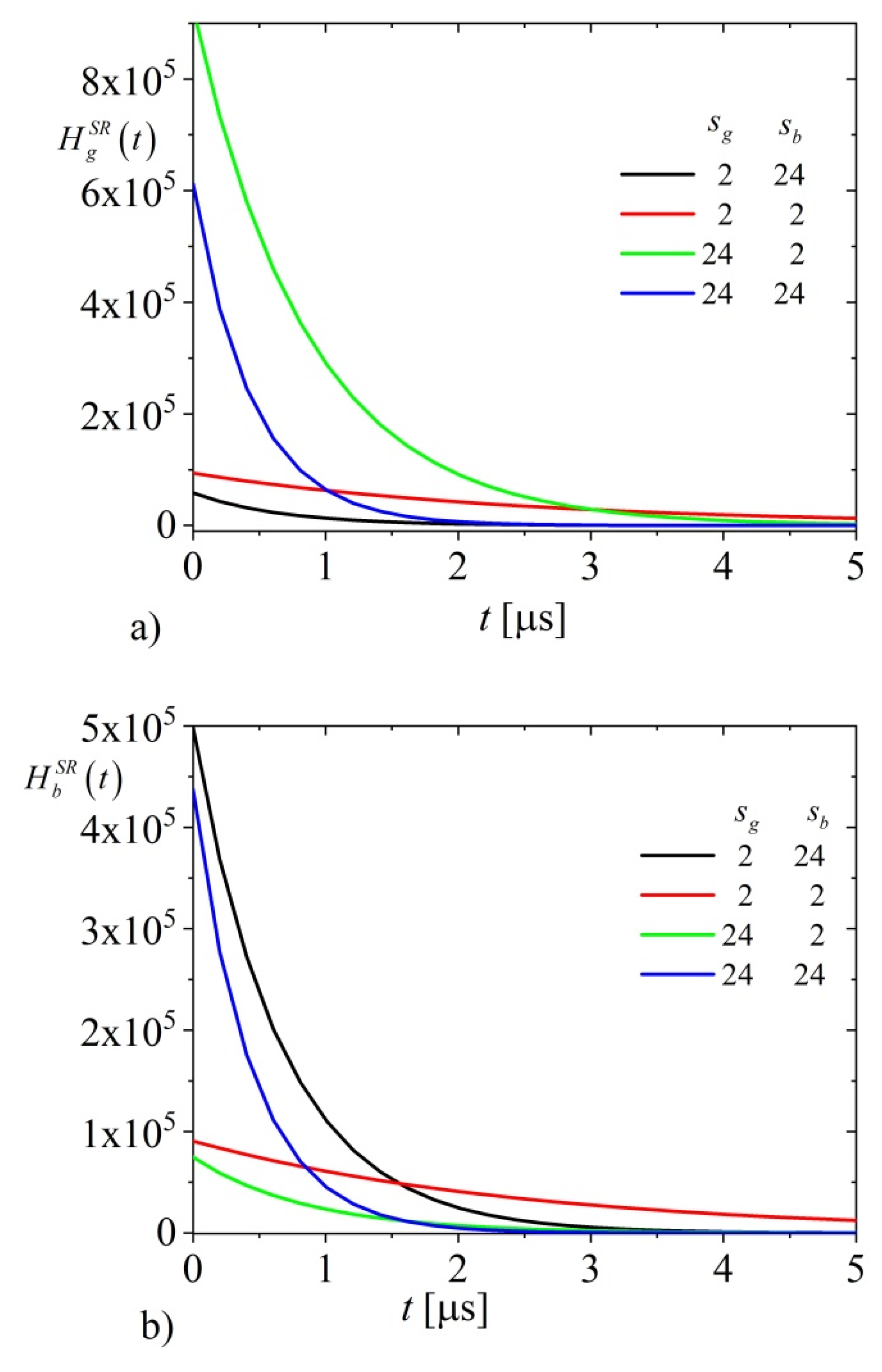
Figure 8.
Influence of and on the evolution of heat sources in a plasma-transparent semiconductor sample upon its excitation by long optical pulses. Time dependence of the recombination heat source: a) on the illuminated side and b) on the non-illuminated side of the sample.
Figure 8.
Influence of and on the evolution of heat sources in a plasma-transparent semiconductor sample upon its excitation by long optical pulses. Time dependence of the recombination heat source: a) on the illuminated side and b) on the non-illuminated side of the sample.
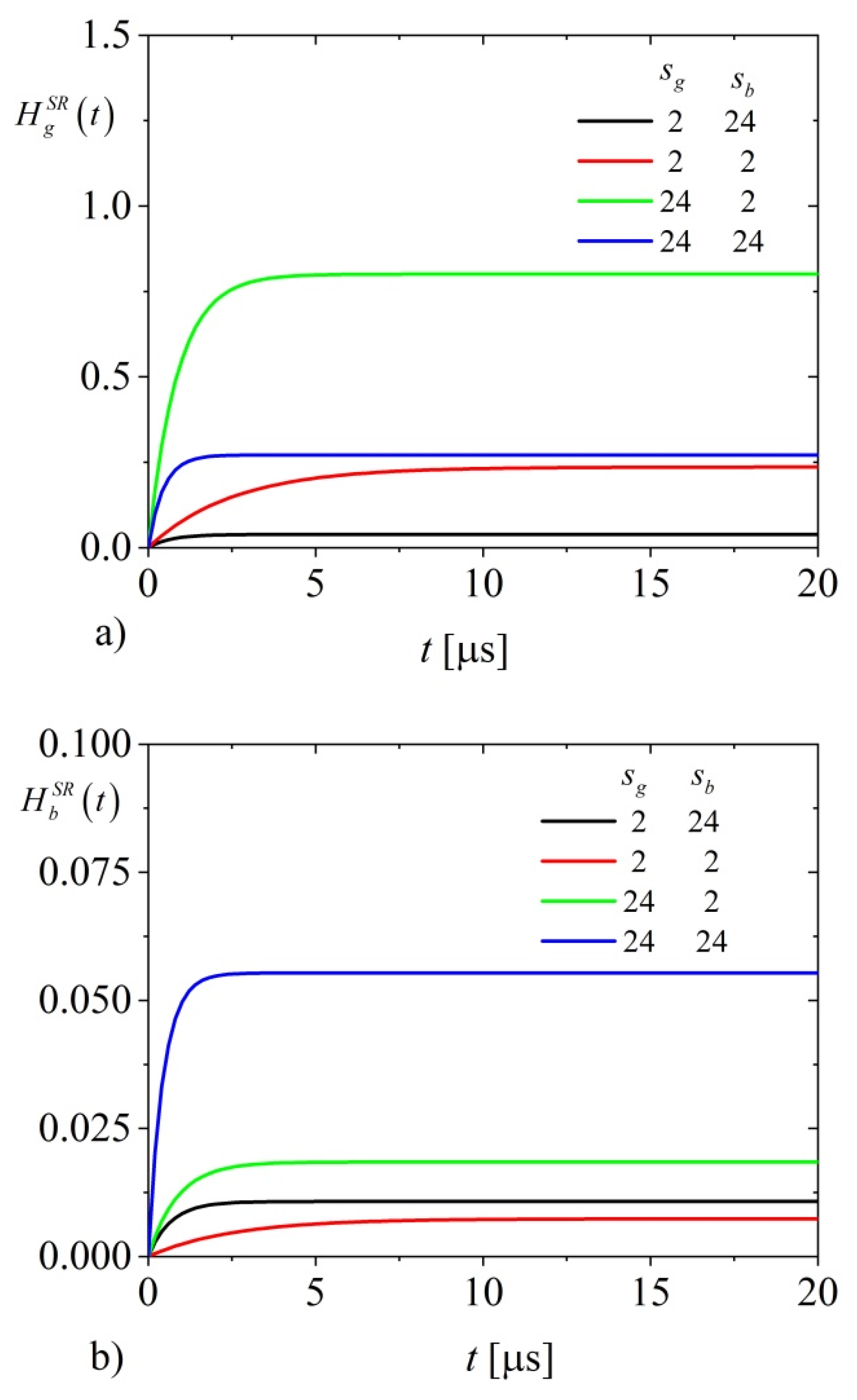

Table 1.
Inverse Laplace transform of an irrational and function with an irrational exponent, [47].
Table 1.
Inverse Laplace transform of an irrational and function with an irrational exponent, [47].
| Complex function | Inverse Laplace transform |
|---|---|
Disclaimer/Publisher’s Note: The statements, opinions and data contained in all publications are solely those of the individual author(s) and contributor(s) and not of MDPI and/or the editor(s). MDPI and/or the editor(s) disclaim responsibility for any injury to people or property resulting from any ideas, methods, instructions or products referred to in the content. |
© 2024 by the authors. Licensee MDPI, Basel, Switzerland. This article is an open access article distributed under the terms and conditions of the Creative Commons Attribution (CC BY) license (http://creativecommons.org/licenses/by/4.0/).
Copyright: This open access article is published under a Creative Commons CC BY 4.0 license, which permit the free download, distribution, and reuse, provided that the author and preprint are cited in any reuse.


