
Submitted:
27 April 2025
Posted:
29 April 2025
You are already at the latest version
Abstract
Radio receivers play a crucial role in wireless communication systems, enabling the extraction of information from modulated RF signals. However, traditional analog-based superheterodyne receivers face limitations such as hardware inflexibility, analog drift, frequency instability, and increased design complexity when supporting multiple modulation schemes. These constraints restrict their scalability and adaptability in modern applications. To overcome these issues, this project adopts a fully digital Software-Defined Radio (SDR) approach implemented through FPGA, offering reconfigurability, parallel processing, and support for real-time communication protocols. The proposed SDR receiver design includes a modular architecture composed of SPI-based ADC interfacing, FIFO buffering to manage clock domain mismatches, digital I/Q signal separation using direct digital synthesis and mixing, and cascaded CIC and FIR filters for decimation and spectral shaping. FM demodulation is achieved using a differential multiplier, followed by a low-pass FIR filter to produce clean audio output. Each subsystem was tested independently and later integrated into a full pipeline, with simulation results confirming accurate signal processing and successful audio reconstruction.
Keywords:
Software-Defined Radio (SDR)
; Field-Programmable Gate Array (FPGA)
; Digital Down conversion (DDC)
; Cascaded Integrator-Comb (CIC) Filter and Finite Impulse Response (FIR) Filter
1. Introduction
Radio receivers play a vital role in wireless communication systems, responsible for extracting actual information from radio frequency (RF) signals from modulated signals. They have applications that vary from broadcast radio and satellite communication to military, navigation, and IoT systems. A radio receiver’s efficiency is determined by how accurately it can decode and process signals. Historically, superheterodyne receivers have been used for a long time in radio design. They operate by converting incoming RF signals into a lower intermediate frequency (IF) using analog mixing and filtering components. Even, though they have excellent selectivity and sensitivity, these analog systems lack hardware flexibility, analog drift errors, Instability in processing, and lack of scalability, making it difficult to use them for different sets of frequency ranges [1]. Furthermore, designing analog circuits for multiple modulation techniques or becomes increasingly complex and not cost-effective. The rise of digital implementations of hardware circuit functionality paved the way for the new type of Radio Transceivers called Software Defined Radio Transceivers. SDR mimics the traditional radio functions such as modulation, demodulation, filtering, up/down converting, and mixing in the digital domain, by executing them through software-driven algorithms rather than fixed analog hardware. This shifting the whole process to the digital domain brings huge advantages like re-programmability, easy upgrade of a wide range of frequencies, and reduced cost compared to traditional hardware receivers [2,3]. SDR also makes the radios much more adaptable to new communication protocols by simply updating the software, which is useful for the development of cognitive radio, and future adaptive wireless systems [4].
Initially, SDRs were developed on general-purpose microcontrollers and dedicated digital signal processors. but the parallel processing performance was limited by the sequential processing nature of those chips. This limitation can be overcome by Field Programmable Gate Array, which provides high-speed parallel processing, Dedicated DSP Slices that performs complex mathematical functions, high power efficiency, and Flexible architecture ideal for various range of frequency signals modulation processing [5]. FPGAs can be synthesized in hardware and verified using simulation software like ModelSim and Matlab. CIC Filters can be designed for Decimation as well as interpolation processes depending upon the place where it is being used [6]. FIR filter, which can be designed for Compensation Filtering is designed and tested using FDA tools and FIR tools like MathWorks. Even the Simulation of FPGAs can also be done using Simulink Software [7]. CORDIC-based Demodulation Algorithms proved to be better in terms of execution speed and hardware occupy compared to Demodulation algorithms developed on Conventional SDR chips [8].
2. Literature
J. Qiang, Y. Gu, and G. Chen developed a robust SPI communication system for FPGA applications using a 16-step state-machine approach in Verilog, enabling high-speed and synchronized full-duplex data transmission [9]. C. Sisterna, M. Segura, and colleagues developed an ultra-high-speed ADC interface using DDR flip-flops, FIFO buffers, and Virtex-II Pro FPGA architecture to eliminate ASIC dependence and allow real-time data acquisition and transfer [10]. N. Narendra, D. Srilakshmi, and M. V. Mohankumar developed a high-speed spectrum processing system using DDC with Numerically Controlled Oscillator (NCO), CIC and FIR filters, and FFT-based detection for SDR systems [11]. M. G. B. Saleem and his team developed a high-performance FPGA-based DUC/DDC framework utilizing Direct Digital Synthesis, CIC filtering, and FIR enhancement, achieving optimized modulation and demodulation for SDR receivers [12]. G. Jinding, H. Yubao, and S. Long developed a linear-phase FIR low-pass filter implemented with the Kaiser Window technique via DSP Builder, achieving efficient FPGA-based adaptive filtering [13]. Y. S. Hon and V. Baste developed a reconfigurable FPGA-based SDR transceiver combining Manchester encoding, BFSK, and FM modulation along with digital demodulation using an all-digital PLL, implemented on Spartan-3 FPGA [14]. F. Yu developed a fully digital FM demodulator using a hybrid delay and phase-adaptive demodulation technique with CORDIC-based vector rotation and filtering, implemented on a Xilinx Virtex-2 FPGA to improve real-time accuracy and speed [15]. B. Ramamurthi, K. Giridhar, and M. A. Srinivas developed a DSP-based FM demodulator for GMSK signals using a limiter-discriminator model with MLSE and Viterbi decoding for error rate improvement [16]. Husnain Al Bustam and Mohammad Shahzamal developed a DAC implementation using SPI-controlled LTC2624 on a Spartan-3E FPGA, written in VHDL, providing real-time signal conversion and output monitoring via oscilloscope [17]. Trio Adiono, Nur Ahmadi, and collaborators developed a pipelined CORDIC-based all-digital FM modulator-demodulator using Verilog on Cyclone II FPGA, improving modulation accuracy and hardware efficiency [18]. Sona Sunny, Jaison Varghese John, and Apren T. J. developed a high-precision CORDIC-based FM demodulator for space communication applications, leveraging vectoring mode and low-pass filtering for accurate phase reconstruction [19]. Ruiqiang Liu and Fengmei Gao developed an FPGA-based RF transceiver system combining PCIe, high-speed ADC/DAC, and multi-standard RF front-end support, enabling flexible SDR deployment in industrial environments [20].
3. Methodology
The methodology we propose will be discussed in this section and shown in Figure 1.
Figure 1 shows the overall system architecture is divided into two parts, the testbench module and the SDR receiver module which includes both digital down-conversion and baseband signal processing. The Testbench module consists of a Test signal generator that generates input ADC signals to SDR design, then a signal serializer that converts the signals into the 12-bit digital data stream, with 3MHz clock frequency and 455KHz frequency. Then, the serialized data is sent to DUT using spi communication.
Figure 2.
Testbench Flow.
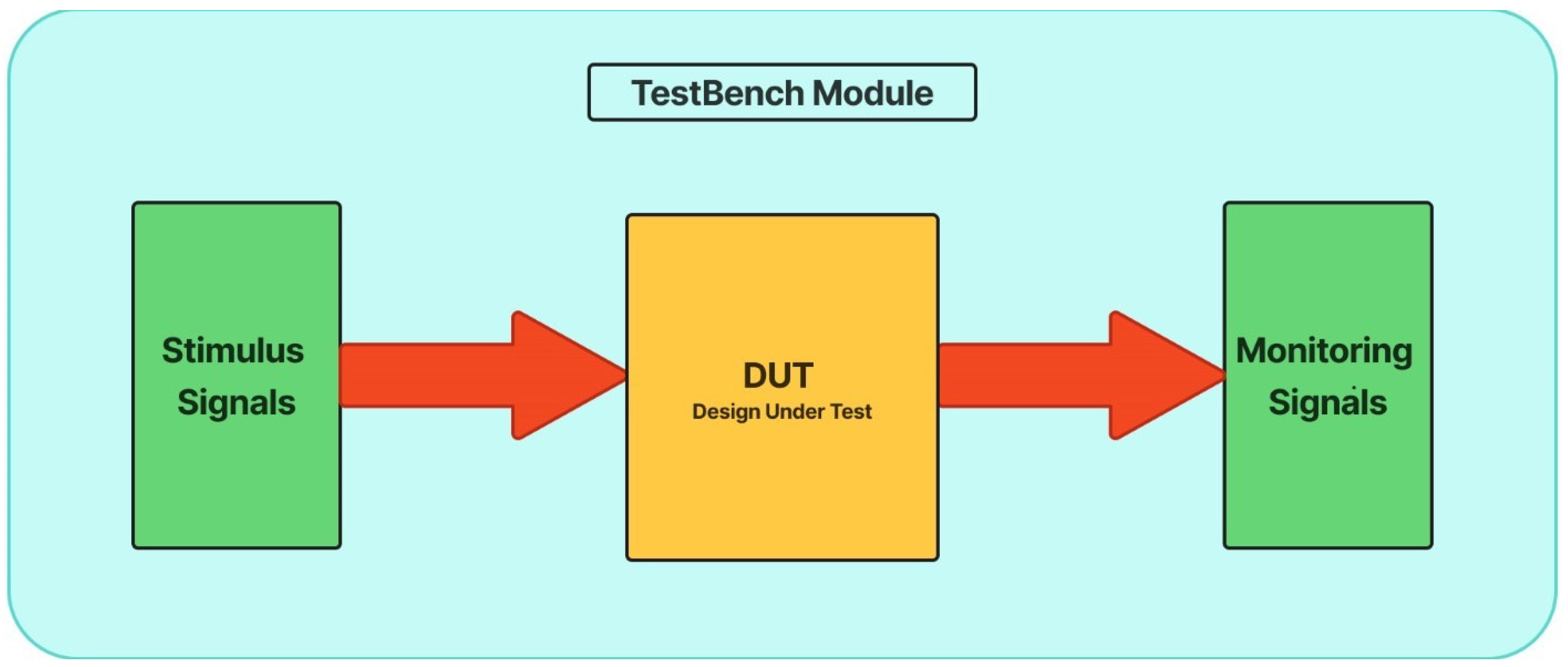
Testbench module is used to verify the functionality of each subsystem that contributes to the software defined radio receiver. For this, a modular verification method is used, where each subsystem is verified individually and then verified by integrating them one by one to verify the overall functionality.
Figure 3 shows the full Pipelined workflow of SDR Receiver. to design a digital down conversion module, which is used to transform high-frequency signals coming from the testbench into low-frequency and baseband signals. This digital down conversion design consists of an ADC Interface module, which is used to extract digital data from testbench signals to the SDR system. Then, the FIFO Buffer is used to slow down the speed of the input signal to match the clock frequency of the SDR system.
To design a direct digital synthesis module, which is used to generate sine and cosine waves of 455KHz frequency to mix them with the incoming signal from the FIFO Buffer module, to produce I (In-phase) and Q (Quadrature) Signals and bring the Signal’s centered frequency to the baseband frequency. Then, the Baseband Signal is passed to the Filtering Module. Filter Section Consists of two filters, CIC Decimation Filter and Compensation FIR Filter.
CIC (Cascaded Integrator Comb) Decimation Filter consists of two sections, the Integrator Section and Comb Section to perform the Low pass Filtering Operations. This Filter Should be designed to Bring the sampling rate of incoming signal from 3MSPs to 46.875KSPs.
-
For this, the Design uses (N=4), (M=2), (D=64).Integrator Section,
- Comb Section,
Compensation FIR Filter serves to correct the passband droop and helps to sharpen the filter response by attenuating unwanted frequencies. The FIR Design is a 100-tap FIR Filter, which has 100 pre-generated FIR Coefficients to compute the output using a tap delay line.
After the Filter Section, the Filtered I and Q Signals are Sent to Baseband Signal Processing to extract the Audio Data from the Modulated Signal. This Section contains Demodulation Followed by a Low-pass Filter to smoothen the Signal one last time. The method used to demodulate the incoming signal is called a differential multiplier. It approximates the derivative of the phase, thereby extracting the frequency deviation information from it.
To Extract the Clear Audio Signal from the SDR Receiver end, a 50-tap FIR Filter is Designed and placed after the Demodulation process. The Coefficients of this Filter are optimized to Filter out the High Frequency Signals above 20KHz, efficiently.
4. Results and Discussion
In this section the Graphical analysis of CIC decimation filter, FIR Compensation Filter and Post demodulation FIR Filter is conducted by using matplotlib. And the simulation results of each individual modules and the simulation results of integrated SDR module is verified by using Model Sim Altera Simulation Software.
4.1. Preliminary Frequency Response Analysis
The CIC filter’s parameter includes the Number of Stages (N), Differential delay (M), and Decimation Factor (D). The decimation factor can be calculated by using the initial sampling rate and expected sampling rate.
Differential Delay is usually 2 for wide-band filtering like audio signals. The more the number of stages, the attenuation in the stopband will be maximum. So, by using the trial-and-error method, the number of stages as 4 attenuates perfectly and the number after this makes very negligible changes.
Figure 4 shows that the CIC decimation filter passes the signals up to 15KHz with –40dbm signal strength and attenuates to –60dbm at 20KHz. At 23KHz the signal strength sharply drops to -250dbm.
Figure 5 shows that the 100-tap fir compensation filter passes perfectly until 17KHz and starts to attenuate sharply, and the signal strength drops below –60dbm around 18KHz.
Figure 6 is the combined filter of both the CIC decimation and fir compensation filter, here the passband is up to 16KHz, and after that, the attenuation starts and reduces the signal strength below –100dbm at 18KHz and the rippling effect of the fir filter is reduced the combination of CIC filter with it.
Figure 7 shows that the 50-tap fir filter for post demodulation portion has a passband up to 15KHz with –50dbm and starts to attenuate to –60dbm at 20KHz, which ultimately attenuates the signal above this frequency.
4.2. Individual Module Simulation Results
The simulation results of individual modules are tested using individual test benches by taking ADC SPI interface and FIFO buffer as one module, DDS and Mixing as one module, CIC and FIR Filters as one Module, and Demodulation and Post Demodulation LPF filter as one Module.
In ADC SPI and FIFO Section, Figure 8 shows that whenever the chip is selected and data is ready from the testbench module, the data_ready shows a high spike, which initiates the data transmission. Miso is the data coming from the Testbench to the ADC interface module, further sent to FIFO Buffer to slow down. FIFO_full being empty all the time proves that the FIFO buffer is not overloading with the input of data.
In the DDS and Digital Mixer Module, the input data is the Simulated 12-bit input data stream with 455KHz frequency sent into the Mixer module. Sine out and Cosine out are the generated Sine and cosine signals with 455KHz, Mixed_i, and Mixed_q are an output of Digital output which is baseband Signal. Figure 9 shows that mixed_i and mixed_q are the product of generated sine and cosine waves and input signal.
In the Filter Section, Low signal and high signal are combined to give d_in which is the input signal of the CIC decimation filter, the input nature of the CIC filter is that it has both low-frequency signal and high-frequency signal, one is below 20KHz, and one is above 20KHz. Figure 10 shows that d_out, an output of the CIC decimation filter, filtered out almost 90% of the high-frequency signal from the input. This signal is given into fir compensation, which further attenuates the high-frequency signal and gives out the smooth low-frequency signal in output called fir_out.
In the Demodulation Section, I_in and Q_in are the In-phase and Quadrature signals generated by the testbench designed for the Demodulation module. They are designed in a way that they vary with frequency and phase over time in a periodic manner. Figure 11 shows that the fm_out_raw is an output of the Demodulation module that merges and converts the I and Q signals into Audio signal form. The high spike from the raw data is fully filtered out by the Post Demodulation LPF Filter and only passes the audio signal through it.
4.3. Integrated System Simulation Results
After Successful verification of all Sub modules individually, the integration is mandatory as the real SDR system works with each module integrated. A new Testbench is designed to imitate all testbench’s functions into one single top testbench. Figure 12 shows that the miso data is from the testbench is passed into the FIFO module then its output is Digital mixer to get I_out and Q_out, which then passed to the CIC filter, which has aliasing output, which is corrected by fir filter and smoothened output is visible from I_fir and Q_fir.
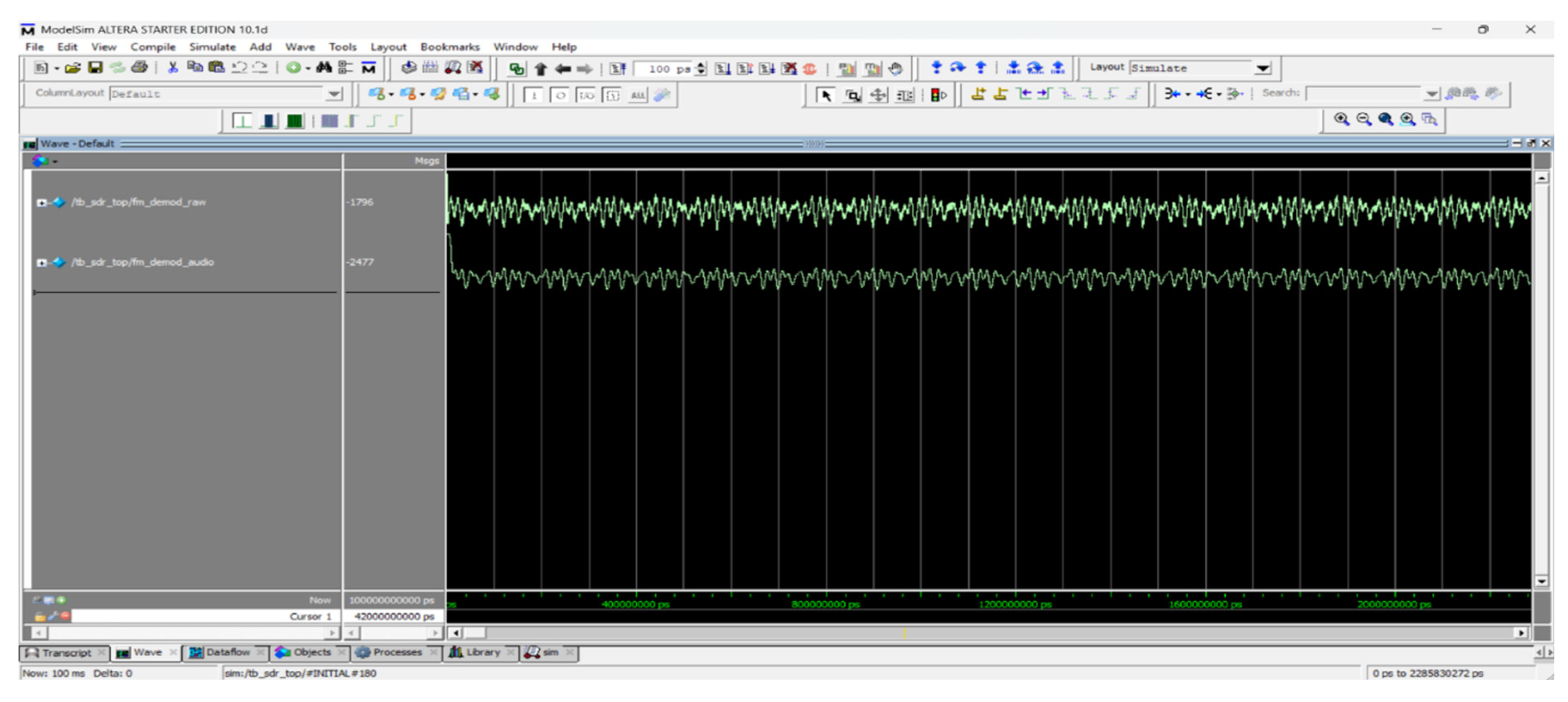
Figure 13 is the extension of the previous graphs; it shows that the I_fir and Q_fir are passed into the demodulation filter with extra special noise produced by the testbench producing a noisy audio signal output. And fm_Demod_audio filters out the high-frequency noise from the output to give clear audio output.
5. Conclusion
In this study, a complete digital Software-Defined Radio (SDR) baseband signal processing system was developed and verified through simulation. The pipeline includes ADC interfacing using SPI, FIFO-based data buffering, digital mixing for I/Q signal separation, decimation via CIC filters, FIR compensation filtering, and FM demodulation using a differential multiplier technique. Each module was individually tested and later integrated into a full system. The input signal was synthetically generated using testbench stimulus, and output verification was performed using simulation graphs. The successful simulation of all stages validated the correctness of the design logic and demonstrated reliable data flow across the processing chain. The results confirmed that the system is functionally complete and ready for hardware implementation.
Future work will focus on extending the design into a real-world prototype. This includes developing the analog RF front end with mixers, filters, and amplifiers to condition antenna signals before ADC conversion. Integration of an actual ADC with FPGA will enable real-time signal processing. Designing a compact PCB combining the analog and digital domains is a key next step. Additionally, optimizing digital components such as FIR filters and mixers using multiplier-less or distributed arithmetic techniques will enhance hardware efficiency. FM demodulation will be upgraded to a quadrature arctangent-based method for improved linearity and noise handling. These enhancements aim to transform the simulated design into a fully functional hardware SDR platform suitable for real-time communication systems.
References
- Kaur, G., & Raj, V. (2008, July). Multirate digital signal processing for software defined radio (SDR) technology. In 2008 First International Conference on Emerging Trends in Engineering and Technology (pp. 110-115). IEEE.
- Mustafa, K. H. (2023). Design and implementation of SDR circuits using FPGA (Doctoral dissertation, FACULTY OF ENGINEERING Electronics Engineering and Electrical Communications Design and implementation of SDR circuits using FPGA A Thesis submitted in partial fulfillment of the requirements of the degree of Master of Science in Electrical Engineering (Electronics Engineering and Electrical Communications) by Kamal Hussein Mustafa Bachelor of Science in Electrical Engineering (Electronics Engineering and Electrical Communications) Faculty of Engineering, Alexandria University).
- S, Jahnavi & B, Pooja & FM, Santro & Vijayageetha, R. (2016). Implementation of Wide Band FM Receiver on RTL-SDR. International Journal of Engineering Research and. V5. [CrossRef]
- Liu, Ruiqiang,Ga, Fengmei. RF Transceiver Circuit FPGA Program Design and Development[J]. International Journal of Future Generation Communication and Networking,2016,9(12):395-404. [CrossRef]
- G. N. Chaubey, Digital Implementation of RF Digital Receiver on FPGA. Indian Institute of Technology, Roorkee, 2014.
- Bhakthavatchalu, R., Karthika, V. S., Ramesh, L., & Aamani, B. (2013, March). Design of optimized CIC decimator and interpolator in FPGA. In 2013 International Mutli-Conference on Automation, Computing, Communication, Control and Compressed Sensing (iMac4s) (pp. 812-817). IEEE.
- Kolawole, E. S., Ali, W. H., Cofie, P., Fuller, J., Tolliver, C., & Obiomon, P. (2015). Design and Implementation of low-pass, high-pass and band-pass finite impulse response (FIR) filters using FPGA. Circuits and Systems, 6(02), 30. [CrossRef]
- Kislal, A. O., Demiray, A., Ceylan, O., & Yagci, H. B. (2015, November). Implementation of a software defined FM mixed demodulator on FPGA. In 2015 23rd Telecommunications Forum Telfor (TELFOR) (pp. 333-336). IEEE.
- Qiang, J., Gu, Y., & Chen, G. (2020). FPGA Implementation of SPI bus communication based on state machine method. In Journal of Physics: Conference Series (Vol. 1449, No. 1, p. 012027). IOP Publishing.
- Sisterna, C., Segura, M., Guzzo, M., Ensinck, G., & Gil, C. (2011, April). FPGA implementation of an ultra-high speed ADC interface. In 2011 VII Southern Conference on Programmable Logic (SPL) (pp. 161-166). IEEE.
- Narendra N, DESIGN OF DIGITAL DOWN CONVERTER AND SIGNAL DETECTION TECHNIQUES FOR SOFTWARE DEFINED RADIO.
- Maruthi, G. B., Kumar, S. P., & Pratap, M. S. (2015). implementation of High performance DUC and DDC for Software Defined Radio Applications. International journal of computer applications, 110(6). [CrossRef]
- Jinding, G., Yubao, H., & Long, S. (2011, March). Design and FPGA implementation of linear FIR low-pass filter based on Kaiser window function. In 2011 Fourth international conference on intelligent computation technology and automation (Vol. 2, pp. 496-498). IEEE.
- N. Kumar, M. Rawat and K. Rawat, "Software-Defined Radio Transceiver Design Using FPGA-Based System-on-Chip Embedded Platform With Adaptive Digital Predistortion," in IEEE Access, vol. 8, pp. 214882-214893, 2020. [CrossRef]
- Yu, F. (2004, September). FPGA implementation of a fully digital FM demodulator. In The Ninth International Conference onCommunications Systems, 2004. ICCS 2004. (pp. 446-450). IEEE.
- Ramamurthi, B., Giridhar, K., & Srinivas, M. A. (1996). DSP-based digital FM demodulation for GMSK signals. Sadhana, 21, 101-112. [CrossRef]
- Al Bustam, H., & Shahzamal, M. A VHDL Based DAC Implementation on FPGA.
- Adiono, T., Ahmadi, N., Renardy, A. P., Fadila, A. A., & Shidqi, N. (2015, August). A pipelined CORDIC architecture and its implementation in all-digital FM modulator-demodulator. In 2015 6th Asia symposium on quality electronic design (ASQED) (pp. 37-42). IEEE.
- SUNNY, S., JOHN, J. V., & TJ, D. A. CORDIC Based FM Demodulator for Digital Telecommand Receiver.
- Liu, R., & Ga, F. (2016). RF Transceiver Circuit FPGA Program Design and Development.
Figure 1.
System Architecture.
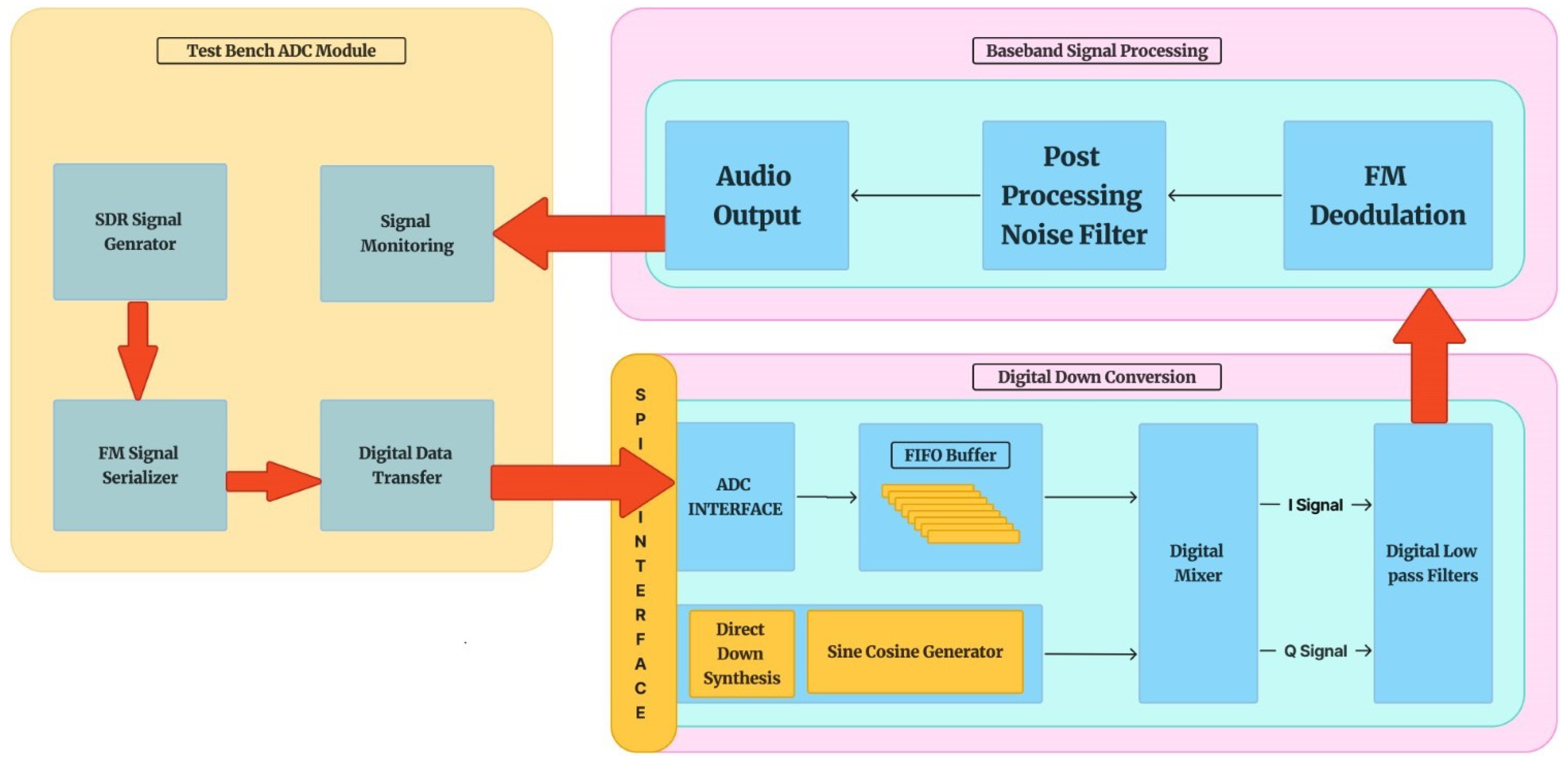
Figure 3.
SDR Receiver Workflow Diagram.
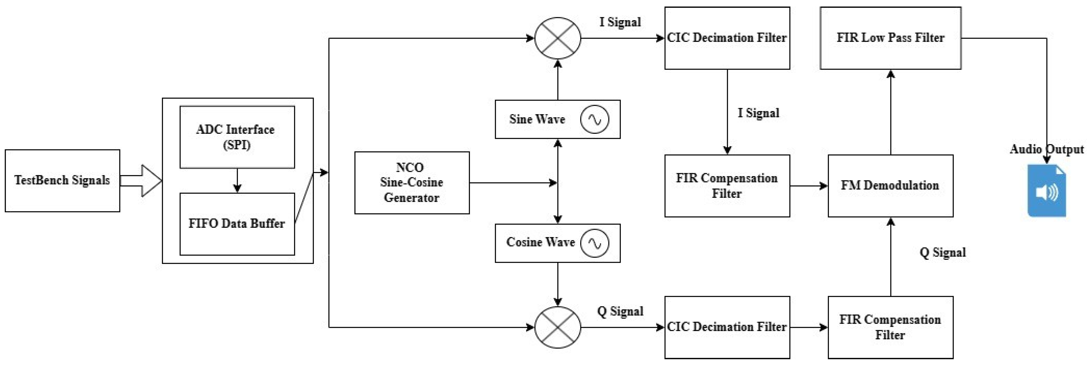
Figure 4.
CIC Decimation Filter Analysis.
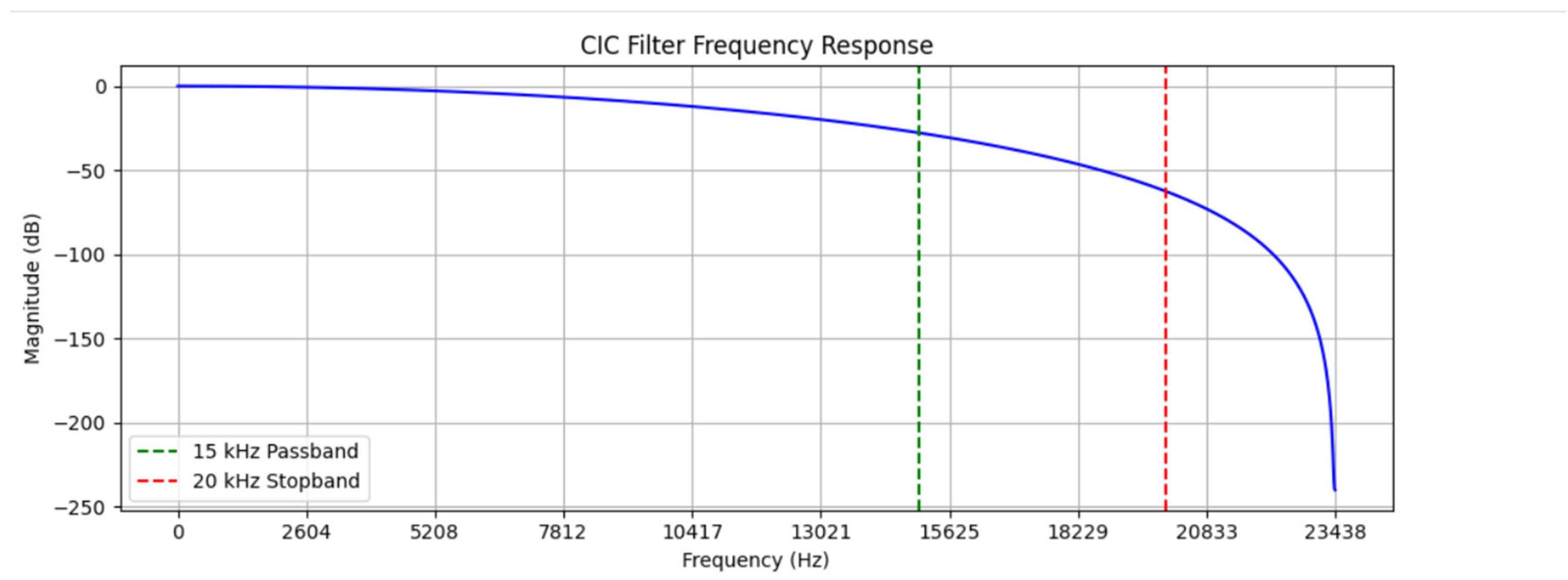
Figure 5.
FIR Compensation Filter Analysis.
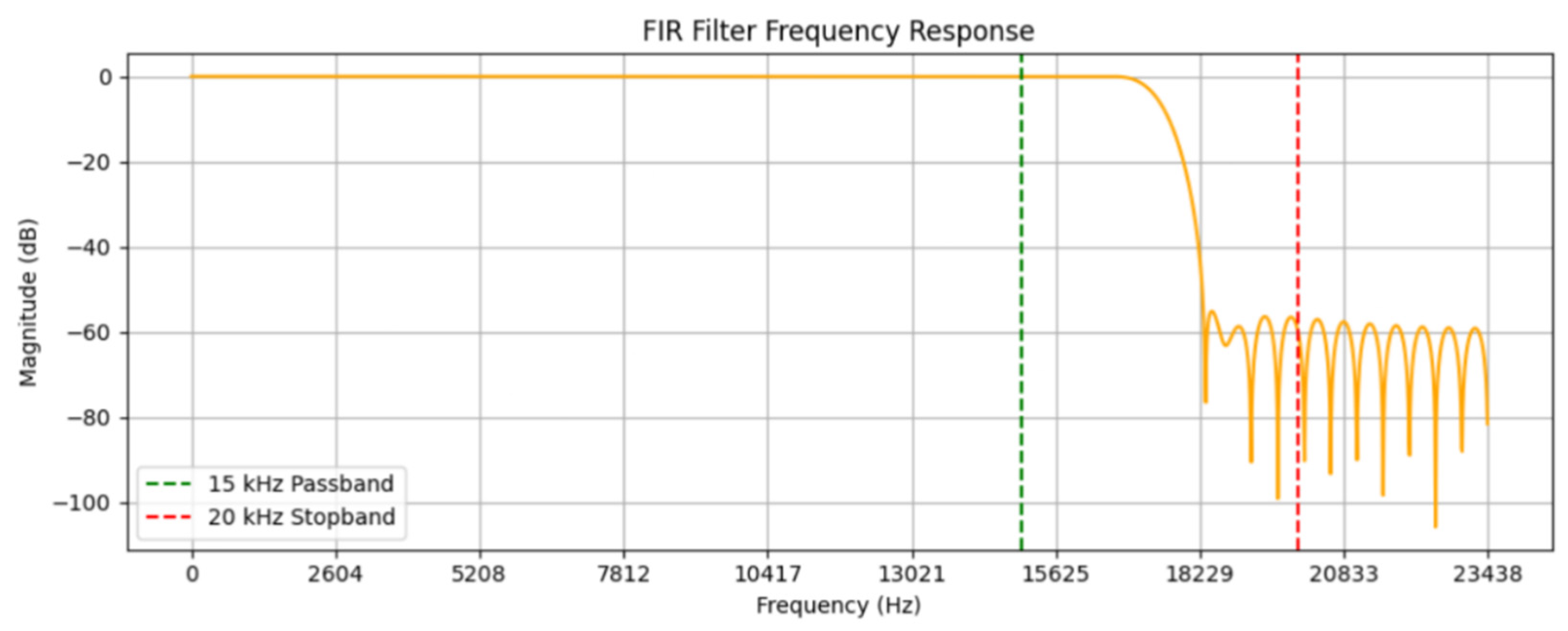
Figure 6.
Combined CIC & FIR Filter Analysis.
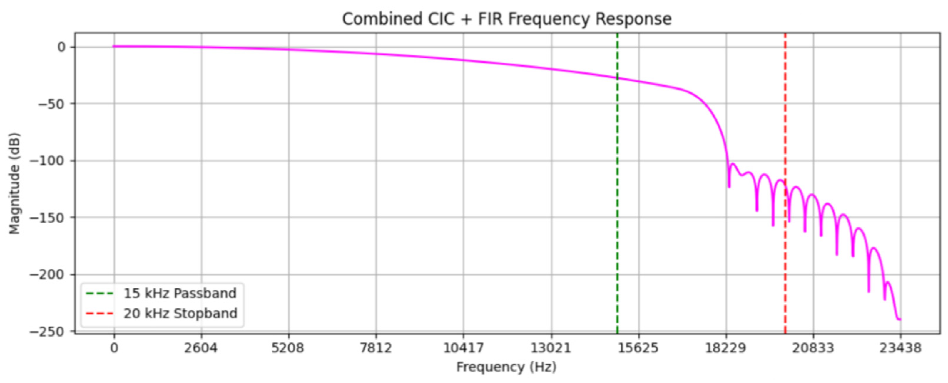
Figure 7.
Post Demodulation LPF-FIR Filter Analysis.
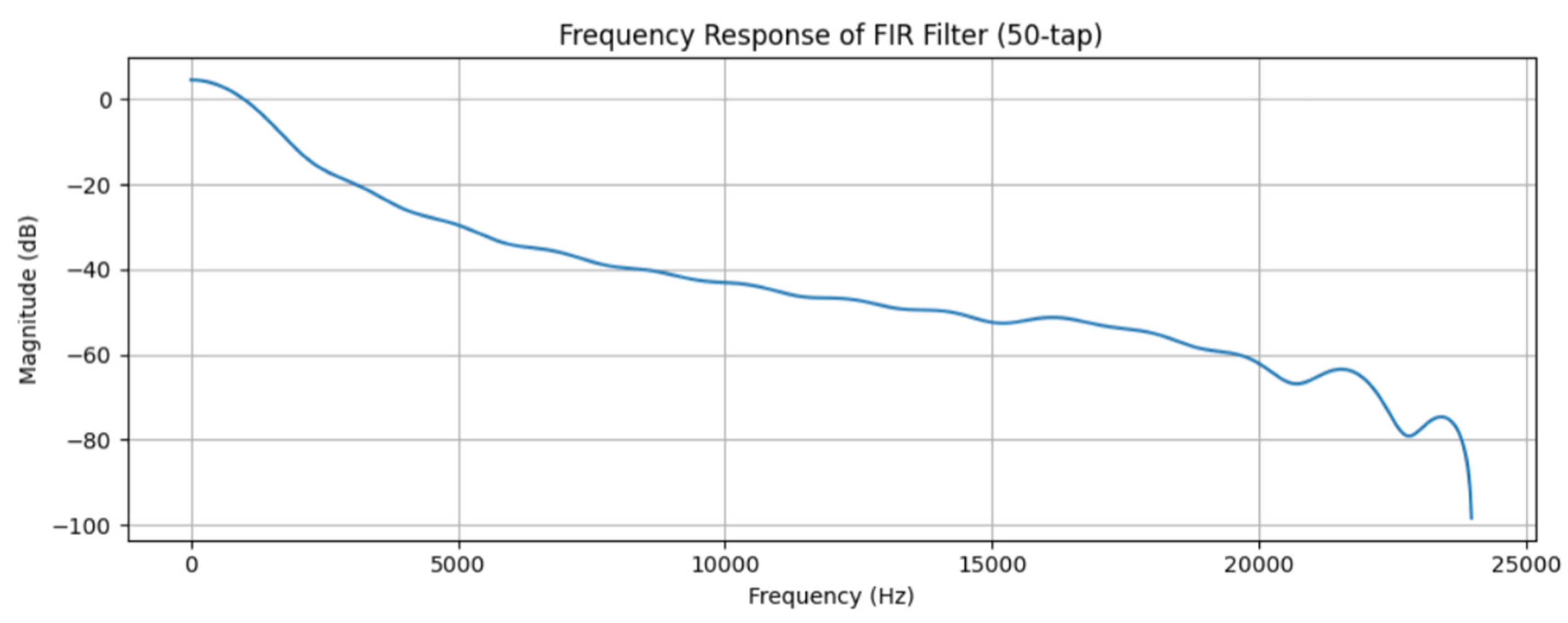
Figure 8.
Simulation Result Graph of ADC FIFO Module.
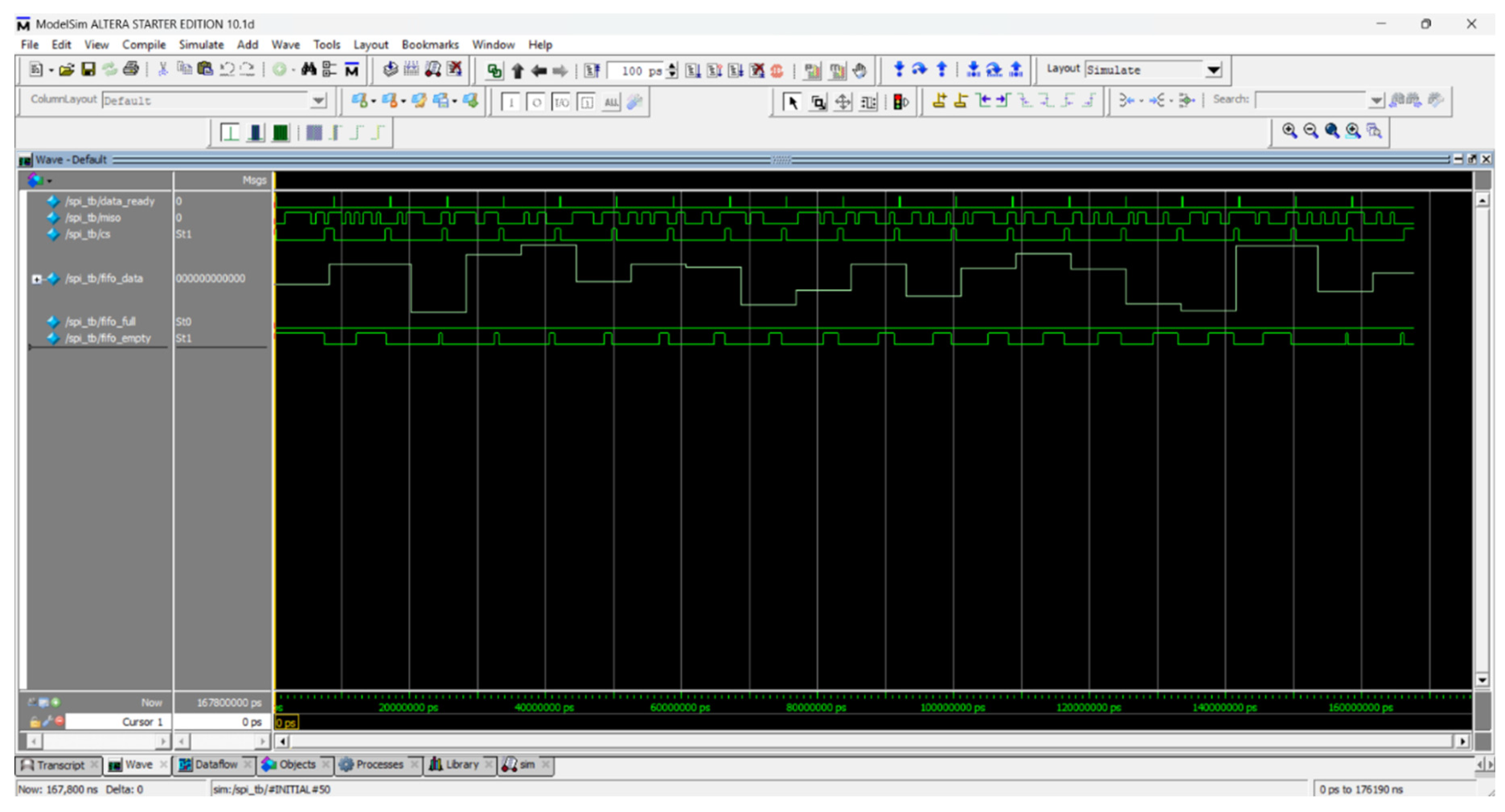
Figure 9.
Simulation Result Graph of Digital Mixer Module.
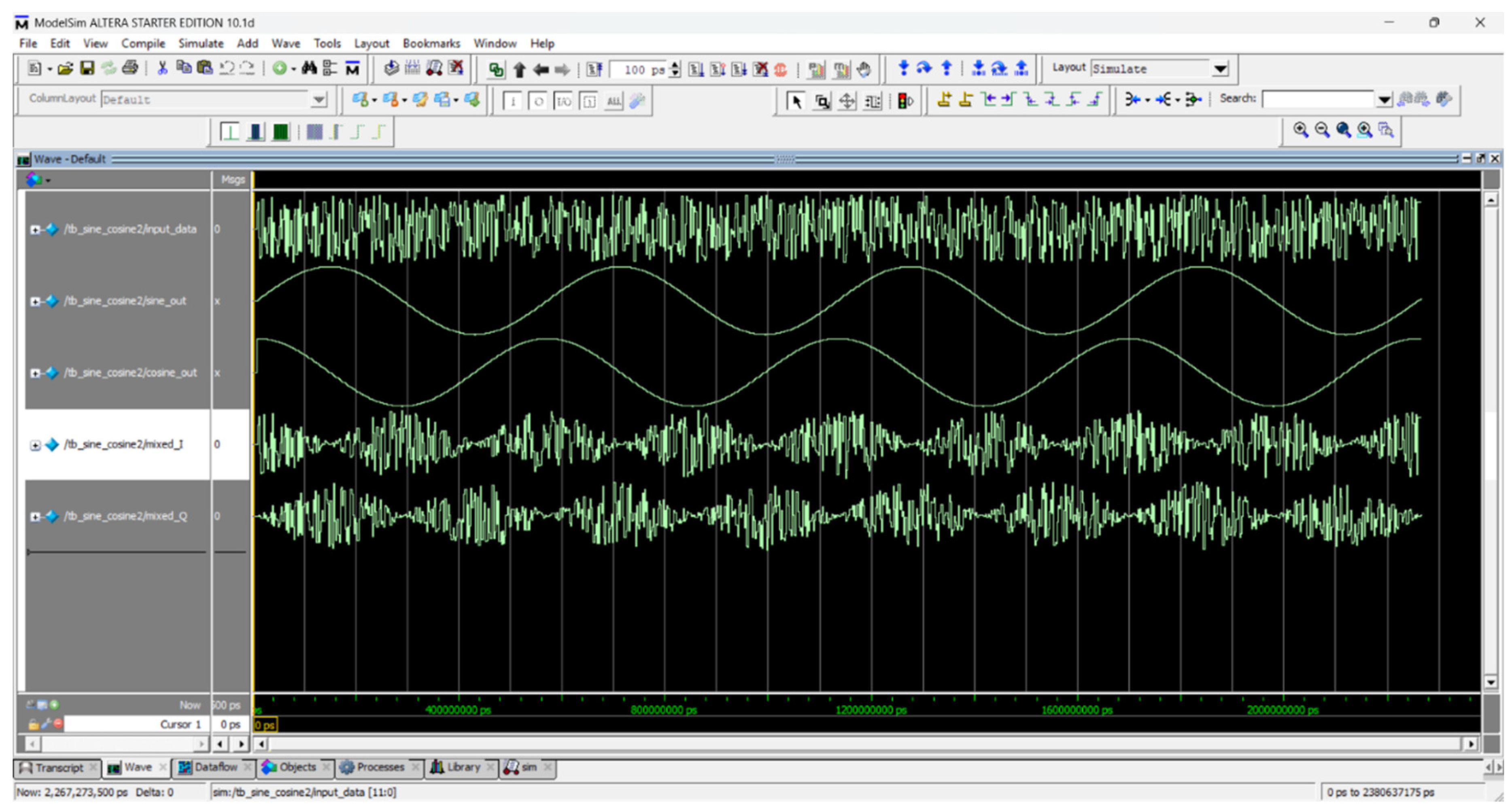
Figure 10.
Simulation Result Graph of CIC FIR Filter Module.
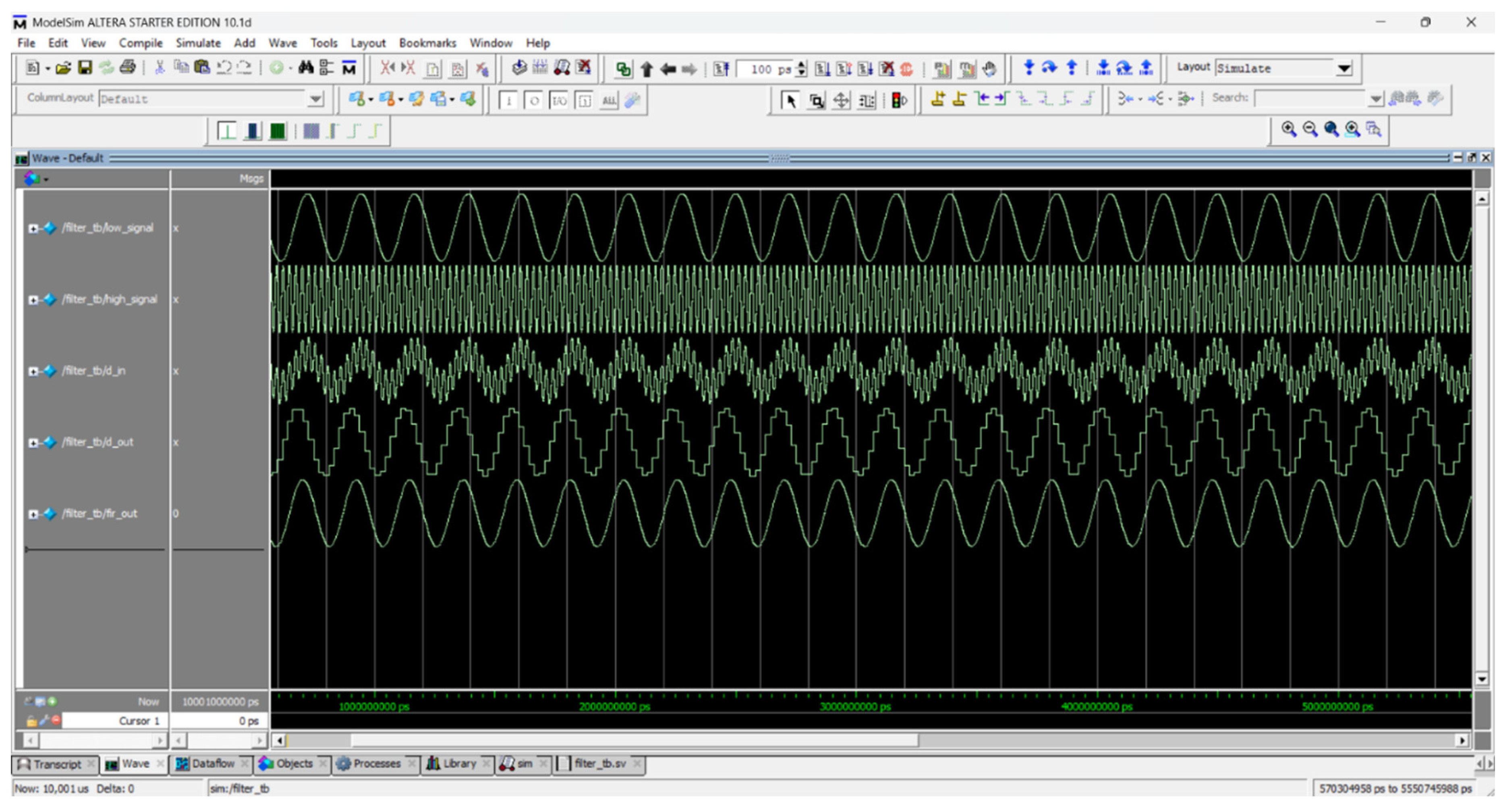
Figure 11.
Simulation Result Graph of FM Demodulation Module.
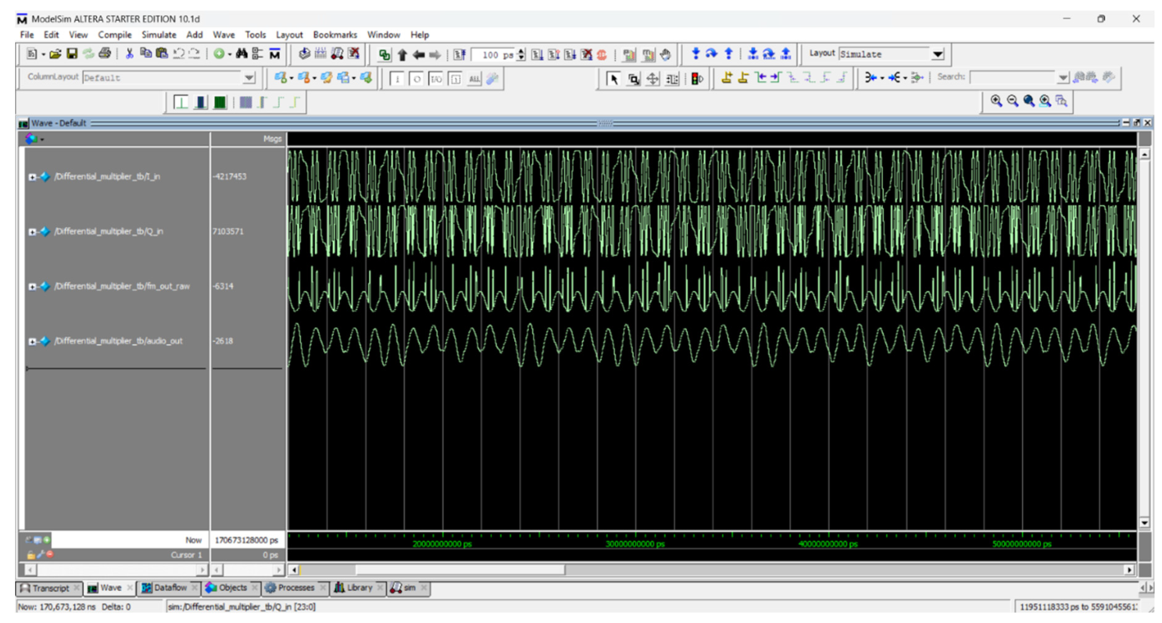
Figure 12.
Simulation Result Graph Integrated SDR System-1.
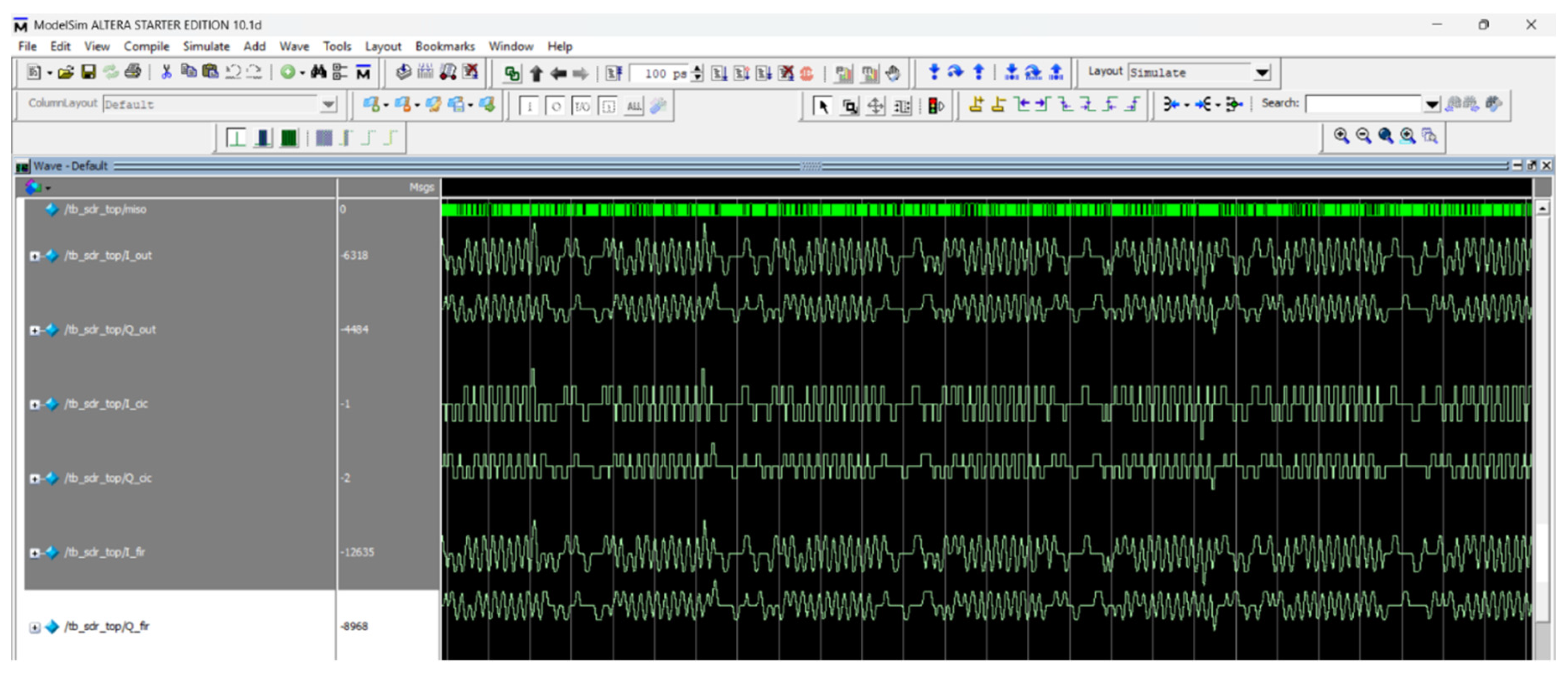
Figure 13.
Simulation Result Graph Integrated SDR System-2.
Disclaimer/Publisher’s Note: The statements, opinions and data contained in all publications are solely those of the individual author(s) and contributor(s) and not of MDPI and/or the editor(s). MDPI and/or the editor(s) disclaim responsibility for any injury to people or property resulting from any ideas, methods, instructions or products referred to in the content. |
© 2025 by the authors. Licensee MDPI, Basel, Switzerland. This article is an open access article distributed under the terms and conditions of the Creative Commons Attribution (CC BY) license (http://creativecommons.org/licenses/by/4.0/).
Copyright: This open access article is published under a Creative Commons CC BY 4.0 license, which permit the free download, distribution, and reuse, provided that the author and preprint are cited in any reuse.


