Submitted:
23 April 2025
Posted:
25 April 2025
You are already at the latest version
Abstract
In this work, we will study basic geometric and electronic structure parameters of hypothetical metaglitter allotropes of silicon, formed by triangular, pentagonal, hexagonal, and octahedral geometries, composed of 6, 10, 12, and 16 atoms. These differ from Si4, which is formed by a square ring interconnected to two others, Si4 anterior and posterior, also by bridges of Si atoms. Its unit cell is composed of 8 atoms. Among its basic electronic characteristics, we will calculate the electron density of all the atoms occupying a unit cell; the electron mobility; the effective mass of free electrons; and the band gap or energy width. We will also study its basic nonlinear optical characteristics, such as first- and third-order susceptibility; and linear and nonlinear refractive index, which characterize these hypothetical allotropes of silicon.
Keywords:
allotrope
; silicon
; body-centered tetragonal ( bct )
; semiconductor
; nonlinear optics
Introduction
Silicon is the most studied primary semiconductor due to its abundance, stability, and low processing and manufacturing costs. This semiconductor has an indirect band gap of 1.12 eV [1]. However, it has efficiency limitations, so the search for new structures that overcome these limitations of basic or elemental semiconductors continues.
Allotropic structures offer new structural and other associated physical characteristics, such as electronic, thermal, and optical conductivity. These new structures can be stable or metastable under ambient temperature and pressure. Examples include the sp3 allotropes Bct-C4; the orthorhombic phase of carbon C14; the forms C, F, M, O, P, W, X, and Z; or the T-12 phase [3].
Theoretical studies are also necessary in the search for new semiconductor allotropes. In this work, we will study the basic parameters of metaglitters [ 2 ], composed of rings of 6, 10, 12 and 16 silicon atoms; where we will study the band gap ( in eV ), electron mobility, electron density, per number of atoms in a unit cell, and effective or dynamic mass of the circulating electrons. We will also study their basic properties in nonlinear optics.
1. Crystal Structure
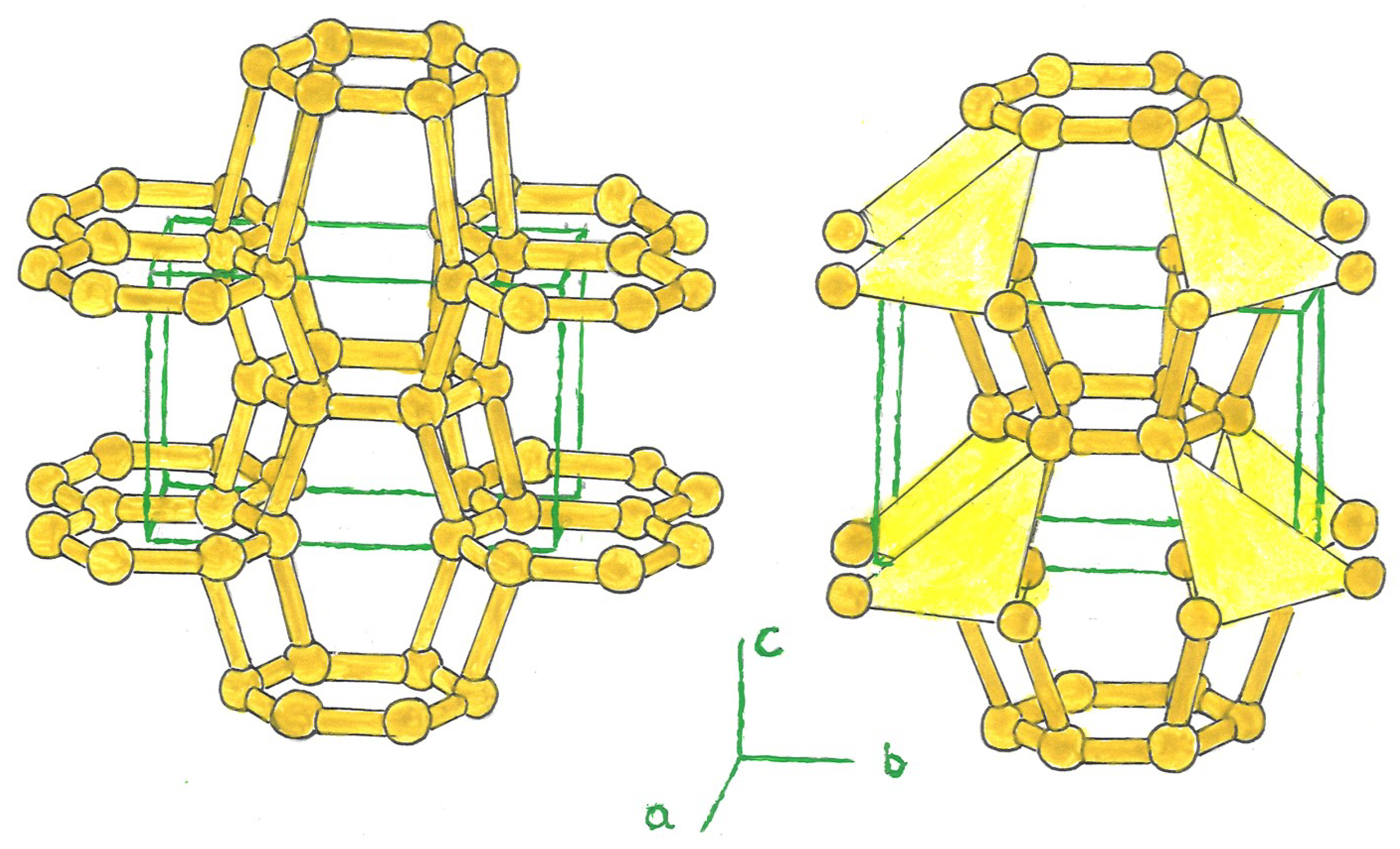
The carbon allotropes, Bct-C4, have been widely studied as an interesting structure. They contain 8 atoms in their tetragonal unit cell [4]. Variant structures derived from this model include, like these, a ring formed by a triangle, pentagon, or hexagon of three, five, or six silicon atoms, centered in the tetragonal cell (bct-Sin, n = 3, 5, 6), bridged with other rings located at the nertices of the tetrahedron; and at the center of the latter, in the case of a triangular or pentagonal ring (Si3, Si5). The unit cell is composed of 6, 10, and 12 silicon atoms, the latter in bct-Si 3, 5, 6. (Figure 1).
Figure 1.
.
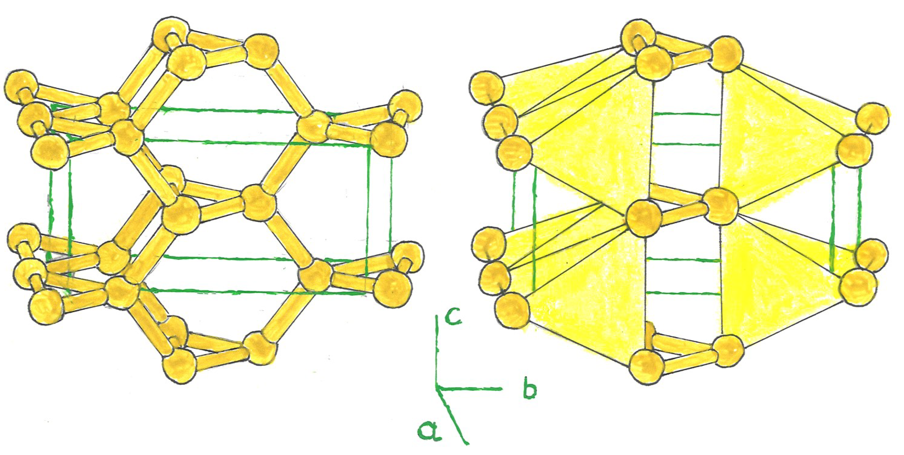
Figure 2.
.
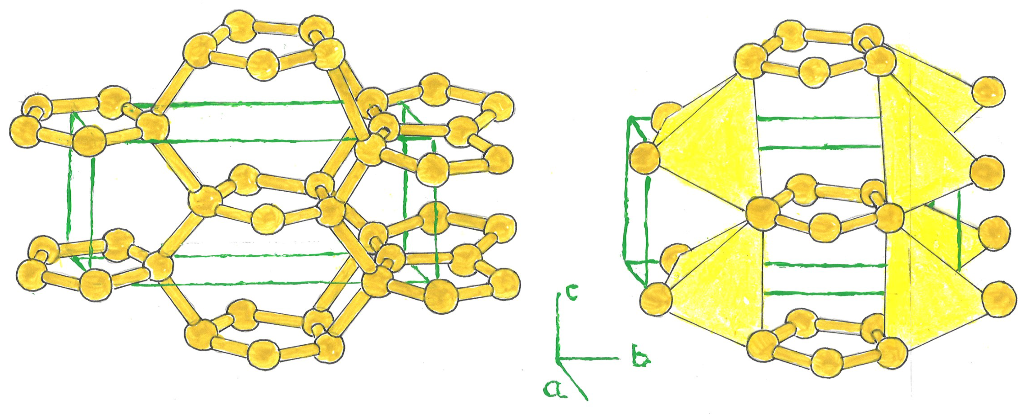
Figure 3.
.
2. Calculation Model
2.1. Electronic Properties
The free-moving electrons of solids, based on the density electrons, were established by the free-electron gas model of Drude and Sommerfeld [4], [5] .

NA is Avogadro's number or constant, Z indicates the valence electron number, A is the atomic weight of the chemical element, ρm is the mass density (mass divided by volume), and ne is the conduction electrons or the number of free electrons. This is the basic equation for calculating their concentration.
For a unit cell, we can simplify the equation to:

In this equation, we substitute the mass density, ρm, for nºA, which is the number of atoms that make up the unit cell [ 6 ].
The effective or dynamic mass of the electron is defined by the formula:
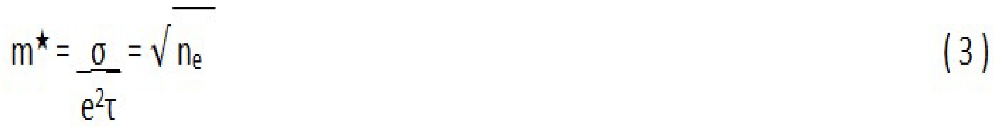
where m* is the effective mass of electrons, σ is the electron conductivity, e is the charge of an electron, and τ is the relaxation time, which is the average time between consecutive collisions of an electron. It is an average value, since not all collisions occur at regular intervals.
There is a relationship between this effective or dynamic mass of free-moving electrons, m*, and the forbidden energy gap or band gap [ 7 ].

And between these and electronic mobility[ 7 ] , which measures the efficiency of semiconductors.


Table 1.
Basic electronic properties of sp3 bct type silicon allotropes - Si3, 5, 6.
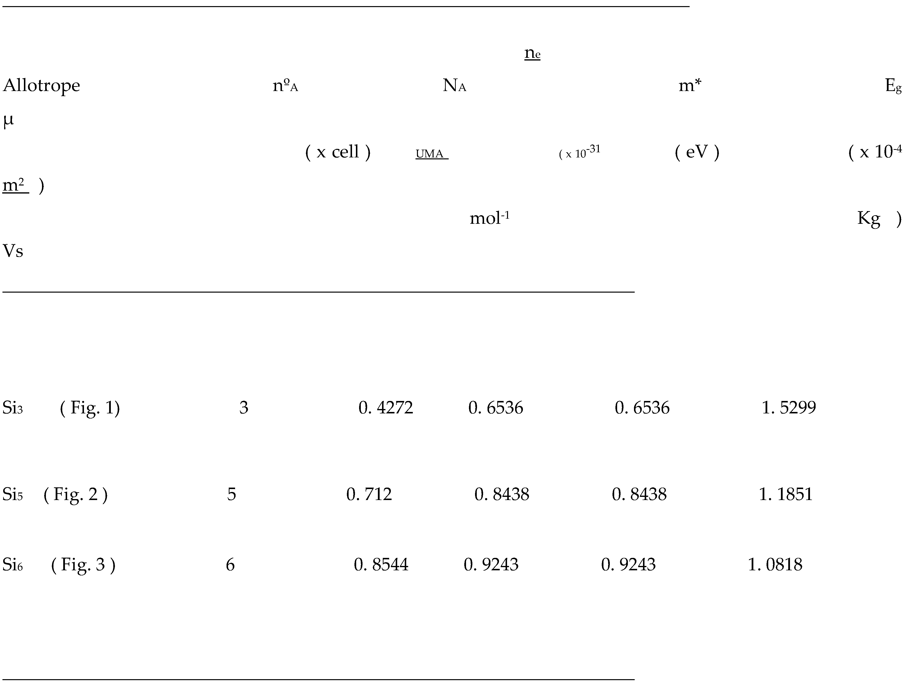 |
Table 2.
Electronic and optical energy band gaps of some elementary semiconductors and the binary compound, GaAs.
Table 2.
Electronic and optical energy band gaps of some elementary semiconductors and the binary compound, GaAs.
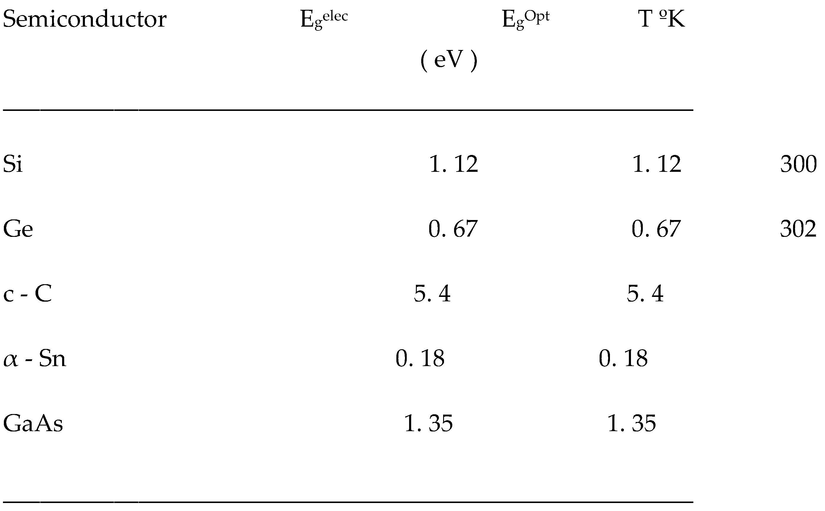 |
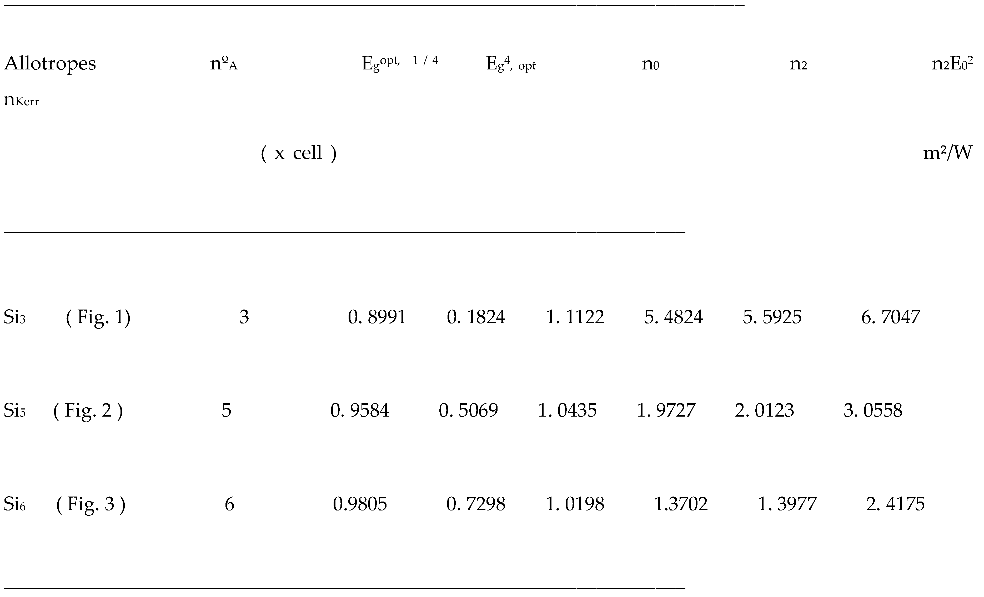
Table 3.
Basic optical properties of sp3 bct type silicon allotropes - Si 3, 5, 6.
 |
2.2. Optical Properties
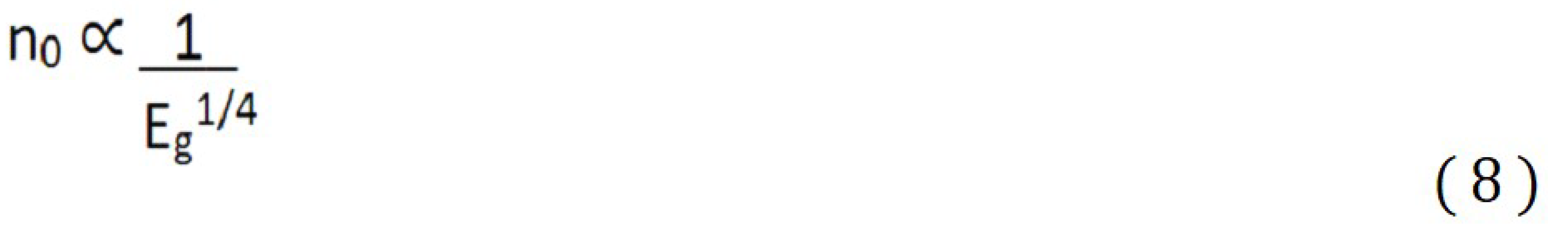
To calculate the basic nonlinear optical properties of any elemental allotrope, we must start from the basic equation to calculate the value of the forbidden energy optical band gap. The basic formula for this gap is:

where E0 = 2Eg opt, is the energy of a simple oscillator.[ 8 ] This formula is based on the Wemple-DiDomenico dispersion relation. The optical band gap is formed in materials that form a high exciton energy. In these, a photon has enough energy to form a bound electron-hole pair or exciton; but not enough to separate the two. It is in this situation that the optical band gap is formed, with lower energy than the transport band. In the optical band gap, photon absorption occurs; while in the transport band gap, non-bound electron-hole pairs are formed. In the vast majority of inorganic semiconductors, the electron-hole attraction that is formed is very small, so the electronic and optical band gaps are almost equal [ 9 ]. In organic semiconductors and single-walled nanotubes, on the other hand, this distinction between both optical and electronic bands can be greater. We have thus, that in inorganics, generally:

There is a relationship between the linear refractive index, obtained ( n0 ), and the optical band gap energy, Eg[ 10 ].
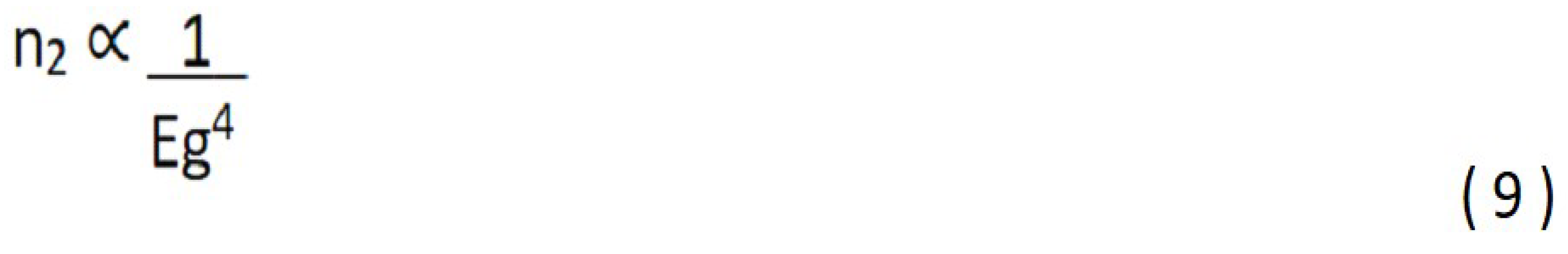
Thus, as a relation, with the non-linear refractive index, n2[ 10 ] :
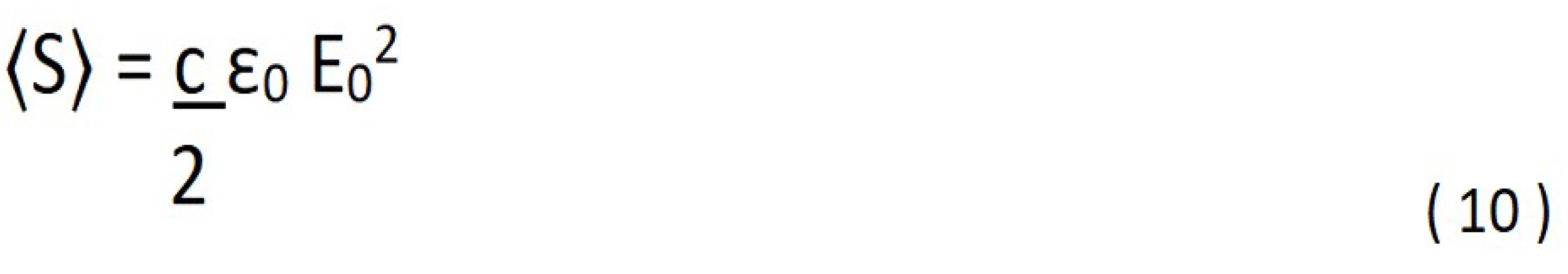
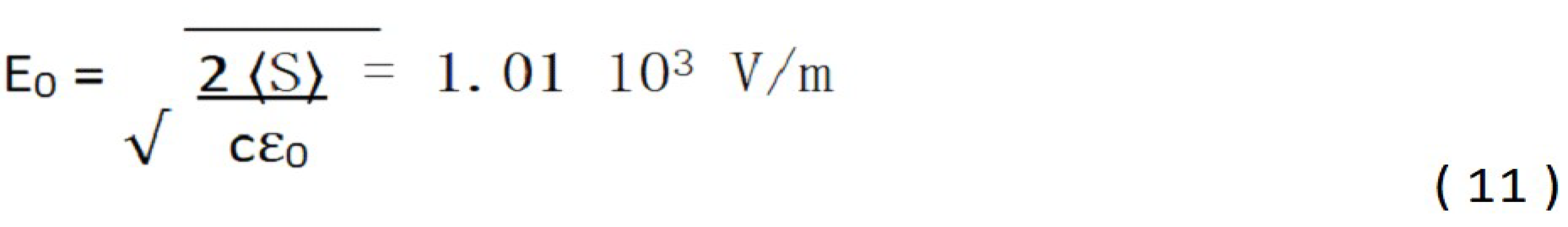
The time-averaged Poynting vector is related to the electric field amplitude [ 12 ] , by:
Finally, the Kerr refractive index will be obtained from the sum of the two refractive indices, linear and non-linear; as well as the electric field E0 [ 12 ] :

Conclusions
The hypothetical sp3 allotropes of bct-type silicon, with 3, 5, and 6 atoms, that have an energy gap closest to that of the diamond-like silicon form (Calc.: 1.0673 eV, Exp.: 1.1 eV), are Si5 (0.9243 eV). The other allotropes have an energy gap somewhat below that of the atoms that form a diamond-like crystal: in the case of Si3, it is 0.6536 eV; in the case of Si5, it is 0.8438 eV. As for non-linear optical properties, Si3 is the one that reaches the highest Kerr index (nKerr), with 6.7047 m2/W . While Si5, with 3.0558 m2/W , and Si6 with 2.4175 m2/W , have obtained lower Kerr index values than Si3.
References
- https://www.valledeelda.com/blogs/valle-de-la-ciencia/47220-alternativas-al-sicilio.html.
- New ultrahard tetragonal C9 and C12 allotropes with edge- and corner-sharing C4 tetrahedra and diamond-like properties. Samir F. Matar 1 and Vladimir L. Solozhenko. May 2023. [CrossRef]
- Stability, electronic and mechanical properties of superhard materials formed by 4 +6 + 8 membered rings of carbon. Junru Koua, Aihua Caoa, Zuo-Hua Liub, Li-Hua Gan. Journal of Solid State Chemistry 277 (2019) 454–465. El Sevier.
- Kittel, Introduction to Solid State Physics, 7th Ed. Chapter 6 Free Electron Fermi Gas.
- vol-1-tipler-mosca-solucionario. Chapter 38.Solids and the Theory of Conduction. Page 2786.
- Combined theoretical and experimental characterizations of semiconductors for photoelectrocatalytic applications. Tangui Le Bahers and Kazuhiro Takanabe. ( Pág. 34 ).
- Analysis of Electron Mobility in Some " Problematic Materials " from Magnetoresistance E ect at High Magnetic Fields. V.V. Shchennikov, A.E. Analysis of Electron Mobility in Some " Problematic Materials " from Magnetoresistance E ect at High Magnetic Fields. V.V. Shchennikov, A.E. Kar'kin,, S.V. Ovsyannikov and N.V. Morozova.
- Optical band gap and refractive index dispersion parameters of AsxSe70Te30−x (0 ≤x ≤30 at.%) amorphous films. Kamal A. Aly. Applied Physics A (2010).
- Optical versus electronic bandgap. Wikipedia.
- Springer Handbook of Electronic and Photonic Materials, Safa Kasap, Peter Capper, Springer, 2017. Pag. 1086 ( Google book ).
- Chapter 13. Maxwell’s Equations and Electromagnetic Waves. Pag. 18 https://web.mit.edu/8.02t/www/802TEAL3D/visualizations/coursenotes/modules/guide13.pdf.
- TRANSITION EFFECT AT THE MEDIUMVACUUM INTERFACE UNDER THE SELF-PHASE MODULATION OF A LIGHT PULSE. S.O. DUDKA, A.I. IVANISIK, A.V. KONOPATSKIY, P.A. KOROTKOV, 2006. http://archive.ujp.bitp.kiev.ua/files/journals/51/2/510205p.pdf.
Disclaimer/Publisher’s Note: The statements, opinions and data contained in all publications are solely those of the individual author(s) and contributor(s) and not of MDPI and/or the editor(s). MDPI and/or the editor(s) disclaim responsibility for any injury to people or property resulting from any ideas, methods, instructions or products referred to in the content. |
© 2025 by the authors. Licensee MDPI, Basel, Switzerland. This article is an open access article distributed under the terms and conditions of the Creative Commons Attribution (CC BY) license (http://creativecommons.org/licenses/by/4.0/).
Copyright: This open access article is published under a Creative Commons CC BY 4.0 license, which permit the free download, distribution, and reuse, provided that the author and preprint are cited in any reuse.


