
Submitted:
25 March 2025
Posted:
25 March 2025
You are already at the latest version
Abstract
This paper presents the design analysis of a low power wideband single-ended CMOS low-noise amplifier (LNA). The proposed topology is based on the modified current reuse circuit to achieve good performance and low power consumption. Two stage current source (CS) amplifiers consume the same DC current which are isolated with large MIMCAPs. The proposed circuit has 2.5 GHz bandwidth which can cover several wireless communication standards (GSM, WLAN and Bluetooth). In first stage a current reuse circuit with shunt feedback is used to satisfy input impedance matching and amplify the signal with minimal noise injection. A common source (CS) with a source follower circuit forms the second stage to improve NF, harmonic distortion and also output impedance matching. The proposed LNA is designed in 65-nm CMOS technology with 2.51 GHz bandwidth that covers frequency range of 0.17-2.68 GHz. The post-layout simulation results show a maximum S21 of 17.24 dB, minimum NF of 2.67 dB, maximum IIP3 of -14.9 dBm, input and output return losses less (S11, S22) than -10 dB while power consumption is 3.52 mW from 1 V power supply. Excluding pads, the proposed circuit occupies 0.45 mm2 silicon die area.
Keywords:
CMOS LNA
; wideband LNA
; noise cancellation technique
; linearity improvement
; low power circuit
1. Introduction
Wideband low-noise amplifiers (LNAs) cover more wireless communication and should amplify with a flat response the weak signal received by the antenna with minimal noise injection. Input impedance matching and linearity with flat response are also two important parameters of a wideband LNA to prevent signal reflections and produce harmonic distortion whole bandwidth [1]. There is a trade-off between mentioned parameters with power consumption [2]. These days the low power designs have received a lot of attention, as most of systems are powered by only a single lithium battery which must work for several days (mobile phone) or even a year (medical devices) that is why designing low-power circuits has become a major challenge for RF designers [3]. LNAs can be designed in two modes of single-ended and differential. Although single-ended LNAs have lower gain and linearity, they are designed easily with good stability and low-noise performance whereas differential LNAs are excellent to achieve high gain and better linearity [4]. Common gate (CG) and common source (CS) circuits are used individually or a combination of both in differential and single-ended LNAs [5]. Although CG topology shows the best performance for a wideband LNA because of the low input impedance of independent of frequency, it needs high power to satisfy input impedance matching and NF, that is why it is not used alone for low power circuits. The CS with shunt feedback is another choice to design a wideband LNA which needs to consume high power to achieve high gain and low NF, that is why it is often used with current reuse technique [6].
The noise cancellation technique is another method for reducing thermal noise with low power consumption which was reported in 2004 [7]. Figure 1a shows conventional current reuse with shunt feedback [2] and Figure 1b noise cancellation LNA [7]. In [9] by using CS and CG a differential LNA has been reported which by using a cross-couple amplifier structure between positive and negative outputs linearity has been improved whole band width without decreasing gain. Although the reported results are excellent, an external RF chock has been used, power consumption is around 12 mW and it is also required a buffer circuit to measure. Authors in [10] has reported a differential LNA by combination of CG and CS in 65 nm CMOS. Although they have obtained high gain, the reported circuit consume 19.8 mW that is very high for low power devices, also the circuit needs an external RF chock. Reference of [11] has presented a differential LNA by using CG and CS. The reported results are reasonable with a 5.7 mw power that cover frequency range of 0.05 to 1.3 GHz; however, an external RF chock has been used. In [12] a differential LNA for sub-GHz applications has been provided which by using a CG and current reuse positive and negative outputs has been formed, respectively. Although the reported power is 3 mW, minimum NF is 3.6 dB that may not be acceptable for some sensitive applications. Kishore and Venkataramani in [13] has presented an inductor less wideband LNA that cover 0.18 to 2 GHz. The presented circuit has used combination of CG and CS, transconductance (gm) is also boosted by using a cross-couple structure between differential nodes. The results were reported in an unmatched output impedance condition, if the buffer current is calculated, the results will become poor. In [14] a shunt-feedback and feedforward technique has been used to design a single-ended wideband LNA which it cancels out noise and distortion simultaneously with ultra-low power of under 1 mW. Although the reported circuit consumes ultra-low power, it needs buffer network to measure and minimum NF of 4.45 dB has been reported which may not be suitable for some applications which need high sensitivity. Yunyou Pu and Wei Li have reported a differential wideband LNA from 0.2 to 3.2 GHz by using CS and CG and noise cancellation technique [15]. Although they have achieved to high gain and minimum NF of 1.4 dB, power dissipation is 17.4 mW that is very high for low power applications. Reference of [16] has presented a single-ended LNA by combination CG, current reuse and noise cancellation circuits for low voltage and low power applications. Although the reported results are acceptable, the area and power of buffer circuit has not been calculated. In [17] a differential wideband LNA by using noise and distortion cancellation technique with 1.6 GHz bandwidth has been provided. The minimum NF of 1.1 dB has been reported, however the power consumption is little high 9.1 mW that is not reasonable for low power systems.
This paper presents a single-ended wideband LNA for low-power applications with an operating frequency in the range of 0.17 to 2.68 GHz. The proposed circuit consists of two stages, a current reuse with shunt feedback and a series inductor peaking technique in the first stage, and a CG and CS form second stage. Both stages consume the same DC current which are isolated from each other by using large metal-insulator-metal capacitor (MIMCAP). By this method power consumption is reduced significantly. Output impedance is also matched to 50 Ω load which does not require an extra buffer network for measurement. The paper is organized as follows. Section 2 analyze the proposed LNA structure in details. Section 3 presents the post-layout simulation results and finally, Section 4 provides the conclusion.
2. Analysis of the Proposed LNA
The proposed wideband LNA with value of elements is shown in Figure 2. The proposed LNA consists of two stages. Transistors of M1, M2 form first stage as a current reuse circuit which DC point in A node is set by a common mode feedback (CMFB) circuit. The length of transistors M1 and M2 is chosen to be slightly longer than the minimum length of the technology used (60 nm) to increase the intrinsic impedance between source and drain (1/gds), which slightly increases the voltage gain at node A [8]. M1, M2 also act as a gm boosting for M5, as a result the signal of A node with again amplification appears in B node. DC point of B node is also set by CMFB2. M8 acts as a shunt- series feedback to meet a wideband input impedance matching and also linearity improvement, this transistor is biased in sub-threshold region to decrease power, besides because gain in B node is high, input impedance matching is satisfied very well without increasing the feedback network coefficient (gm8). Transistors of M3 and M4 form second stage of the proposed LNA which consumes the same DC current as first stage and are isolated from first stage by capacitor of CB1. M3, M4 act as a buffer stage which are used for output impedance matching. Gate terminal of the M4 is also connected to input (node of C) and acts as noise and distortion cancellation technique to improve slightly gain, NF linearity. It means that the noise and harmonic distortion returned by the feedback network is slightly amplified by this transistor with a 180˚ phase difference and summed with the output, which reduces distortion and noise.
Inductor Lg is used to help flat gain, input impedance matching and slightly bandwidth. The details of the input impedance matching, voltage gain, NF, and linearity of the proposed balun-LNA are presented in the following.
2.1. Input Impedance Matching
Figure 3 shows the small-signal model of input of the proposed wideband LNA to calculate the input impedance. The inductor Lg more or less compensates parasitic capacitors (CP) for frequencies of above 1.5 GHz to satisfy input impedance matching whole desired bandwidth (0.17 to 2.68 GHz).
According to the Figure 3, the input impedance of the proposed LNA is approximately calculated as follows:
where , and CP is parasitic capacitors of D node that approximately equals:
Based on the Equation (1), when Lg and CP are resonated, the input impedance tends towards zero which causes S11 to be spoiled, however the amount of the resonance frequency is around 6 GHz that is much more than desired bandwidth (0.17 - 2.68 GHz).
2.2. Voltage Gain
Figure 4 shows AC model of the proposed circuit. As is clear, first stage is formed by M1, M2 M5, M6 and feedback of M8. Transistors M3 and M4 form second stage.
By considering an output load of RL of 50 Ω, voltage gain can be approximately calculated as follows:
where . Inductor Lg and parasitic capacitors are not considered in Equation (3) to simplify calculation and better understanding, however the effect of Lg on the gain is explained below.
The inductor Lg acts as a series inductive peaking to compensate parasitic capacitors of D node. Figure 5 shows effect of Lg on the gain, as shown, it is clear that before the current reuse stage, a passive gain is created by the inductor Lg at D node, which contributes to increase the 3dB bandwidth.
2.3. Noise Analysis
Considering the proposed circuit consists of two stages, according to the Friis equation, it is clear that the first stage has the main effect on NF [2]. Although M4 is connected between the input and output as a CS and can play the role of noise cancellation technique [7], the conditions for complete cancellation cannot be met due to the low-power design and also the connection of a 50 Ω load to the output. In other words, the noise sampling coefficient by the M8 feedback is much lower than its amplification by M4 with RL of 50 Ω that is why it has low effect on NF improvement. In first stage, thermal noise of M5 and M6 can be ignored because they have a degenerated impedance in their source terminals [2]. Transistor M8 is biased in sub-threshold region and low current by a large resistor of R1 to decrease power dissipation, although shot noise is comparable to thermal noise in this regime [18], as a result it can also be ignored because seen impedance in this node (node of C) is too small by around Rs. As a result, main noise depends on current reuse stage, so NF is calculated as following:
where γ is the correction factor which is assumed to be the same for NMOS (M1) and PMOS (M2) for simplicity. According to Equation (4), because the value of is much higher than one, the (4) is simplified to (5).
According to Equation (5), obviously, the greater the effect of the feedback network of M8 , the worse the NF will be.
2.4. Linearity Analysis
Usually, both types of LNAs (single-ended and differential) are designed in one stage to achieve good linearity [2]. In a non-ideal amplifier signal is approximately amplified as [2]:
where α1 is as the small-signal gain. In differential LNAs due to the output differential signal, second term of (6) can be decreased significantly [2], but third order harmonic is still problematic [9].
Figure 6 illustrates the mechanism of linearity improvement of the proposed circuit. If two interferer signals of is applied to input, a third order harmonic of and is produced in output of first stage of current reuse (A node). The produced harmonic node of A comes to node of B through M5 and is also brought to input (node of C) through feedback of M8 then it is amplified with 180˚ phase different by M4 that can decrease the distortion of output and improve linearity [7]. Based on the Figure 6, in the proposed circuit the conditions for complete harmonic cancellation are not provided, because the harmonic appeared in node B reaches node C with a large attenuation coefficient which transistor M4 cannot fully compensate this attenuation in output due to low power design and consequently low gm4, which is why linearity of the proposed LNA is improved by slightly less than 2 dB.
3. Simulation Results
The proposed low power single-ended wideband LNA is suitable for low power Mult-standards receivers which cover the frequency range of 0.17-2.68 GHz such as (GSM, WLAN and Bluetooth). The proposed LNA is designed in 65 nm CMOS technology with 1 V supply voltage and a reference current (IREF) of 50µA for bias network to improve circuit stabilization under process, supply and temperature (PVT) variations. Figure 7 shows the layout of the proposed LNA with a core area of 0.45 mm2. The results of the proposed wideband LNA across PVT and corner variations are presented in Figure 8 and Figure 9, respectively. As shown, S11 and S22 have a value of less than -10 dB over the entire desired bandwidth, also the power gain (S21) and NF have an amount of more than 15 dB and less than 3.24 dB over the desired bandwidth, respectively. Figure 10 shows stability factor (Kf) that has an amount of more than 1 from 0.1 to 12 GHz which means the proposed circuit is unconditionally stable.
To ensure the value of the inductance and quality factor (Q) of the Lg, electromagnetic (EM) simulation has been performed. Figure 11 and Figure 12a demonstrate substrate stack map of 65 nm CMOS technology and inductor Lg for EM simulation. Figure 12b illustrates EM simulation of Lg which values of inductance and Q-Factor at 2 GHz are obtained 5.9 nH and 13.9, respectively. The Self-resonant frequency (SRF) is also around 9 GHz that is a reasonable value for the desired bandwidth (0.17 to 2.68 GHz).
As mentioned in the linearity analysis section, M4 improves linearity. To prove it, IIP3 is simulated in two cases that is shown in Figure 13a,b. Once when the terminal gate of M4 is connected to the input and M4 acts as a CS which the mechanism of distortion improvement is carried out and once when M4 acts only as a current source for second stage. Figure 14a,b show intercept point three (IIP3) at 2.4 GHz and IIP3 versus input frequency, respectively. As shown in Figure 14a, by simulation of two-tone tests with 10 MHz spacing at 2.4 GHz when M4 is as CS, an IIP3 of -14.9 dBm is achieved. Figure 15b, shows both curves of IIP3 at entire desired bandwidth when M4 acts as CS and current source, respectively. As shown the IIP3 is improved when M4 acts as a CS. Table 1 summarizes the results of the proposed wideband LNA in different corners and temperatures. Although the proposed LNA show a small variation in different corners, it is robust against corner and temperature variations. Table 2 represents a comparison to state-of-the art work between the proposed LNA and some similar recent works. Figer of merit (FoM) are calculated as follow [16]:
Excluding [15] which has a fully output impedance matching, other cited references only have reported the LNA core power, that is why some of them has a FoM of higher than the proposed circuit. Only [12] has mentioned the output buffer power of 9 mW, which would make its FoM much lower if it were included. The results of the proposed LNA are reported without using extra output buffer and under conditions of fully output impedance matching. One of the advantages of the proposed topology used is to perform output impedance matching without high power consumption.
4. Conclusions
In this paper, a low power wideband single-ended LNA is analyzed and presented which cover 0.17 to 2.68 GHz and is suitable for low power multi-standards wireless applications. By using two stages of amplifier with same DC current and noise and distortion cancellation method all parameters of a wideband LNA have been satisfied plus output impedance matching in a low power design. One of the advantages of the proposed LNA is a fully output impedance matching with low power consumption so no additional buffer is required for measurement.
References
- Wan, Qiuzhen, Jiong Liu, and Simiao Chen.” An Inductor less Gain-Controllable Wideband LNA Based on CCCIIs.” Micromachines, 2022, 13.11, 1832.
- Razavi, Behzad. RF microelectronics. Vol. 2. New York: Prentice Hall, 2012.
- Mir-Moghtadaei, Sayed Vahid and Farshad Shirani Bidabadi. “A CMOS 3.5 GHz Bandwidth Low Noise Amplifier using Active Inductor.” AUT Journal of Electrical engineering, 2025.
- B. Hu, X. P. Yu, W. M. Lim and K. S. Yeo, “Analysis and Design of Ultra-Wideband Low-Noise Amplifier with Input/Output Bandwidth Optimization and Single-Ended/Differential-Input Reconfigurability,” in IEEE Transactions on Industrial Electronics, 2014, vol. 61, no. 10, pp. 5672-5680.
- Shirani Bidabadi Farshad & Mir-Moghtadaei Sayed Vahid. “An Ultra-Wideband 0.1–6.1 GHz Low Noise Amplifier in 180 nm CMOS Technology”. Journal of Circuits Systems and Computers, 2020, 30, 2150104.
- K. -W. Cheng, W. -W. Chen and S. -D. Yang, “A Low Power Sub-GHz Wideband LNA Employing Current-Reuse and Device-Reuse Positive Shunt-Feedback Technique”, IEEE Microwave and Wireless Components Letters, 2022, vol. 32, no. 12, pp. 1455-1458.
- F. Bruccoleri, E. A. M. Klumperink, and B. Nauta, “Wide-band CMOS low-noise amplifier exploiting thermal noise canceling” IEEE J. Solid-State Circuits, 2004, vol. 39, no. 2, pp. 275–282.
- Hu, S., Du, J., Chen, P., Nguyen, H. M., Quinlan, P., Siriburanon, T., & Staszewski, R. B. “A Type-II Phase-Tracking receiver”,IEEE Journal of Solid-state Circuits, 2021, 56, 427–439.
- Bahareh Shirmohammadi, & Yavari, M. “A Linear Wideband CMOS Balun-LNA With Balanced Loads”, IEEE Transactions on Circuits & Systems II Express Briefs, 2021, 69, 754–758.
- S. Kim and K. Kwon, “A 50-MHz-1-GHz 2.3-dB NF noise- cancelling balun-LNA employing a modified current-bleeding technique and balanced loads”, IEEE Transaction on Circuits and System I, 2019, Reg. Papers, vol. 66, pp. 546–554.
- S. Kim and K. Kwon, “Broadband balun-LNA employing local feedback gm-boosting technique and balanced loads for low-power low-voltage applications,” IEEE Transaction on Circuits and System I, 2020, Reg. Papers, vol. 67, no. 12, pp. 4631–4640.
- S. Tiwari and J. Mukherjee, “An inductor less wideband Gm-boosted balun LNA with NMOS-PMOS configuration and capacitively coupled loads for sub-GHz IoT applications”, IEEE Trans. Circuits Syst. II,2021, Exp. Briefs, early access.
- K. H. Kishore, B. Venkataramani, R. Sanjay, and V. S. Rajan, “High gain inductor less wideband Balun-LNA using asymmetric CCC & BIST using RMS detectors”, AEU-International Journal of Electronics and Communications”, 2019, vol. 105, pp. 135–144.
- H. U. Mahmood, S. -G. Lee and J. Kim, “A 0.1–4.2 GHz, 960-μW Inductor-Less and Negative Shunt Feedback LNA With Simultaneous Noise and Distortion Cancellation and Bandwidth Extension”, IEEE Transactions on Circuits and Systems I, 2024, Regular Papers, vol. 71, no. 6, pp. 2563-2575.
- Pu, Y., Li, W., Li, Q., Ma, X., & Xu, H. A 0.2–3.2-GHz active Balun-LNA with 1.4–2.18-dB NF utilizing asymmetric current distribution in 28-nm CMOS. IEEE Microwave and Wireless Technology Letters, 2025.
- Z. Liu, C. Chye Boon and Y. Dong, “A 0.6 V, 1.74 mW, 2.9 dB NF Inductor less Wideband LNA in 28-nm CMOS Exploiting Noise Cancellation and Current Reuse,” in IEEE Transactions on Circuits and Systems I, 2024, Regular Papers, vol. 71, no. 8, pp. 3561-3572.
- J. -W. Park, D. -Y. Kim and D. Im, “A Broadband Gm-Boosted Active Feedback CMOS Low-Noise Amplifier for Low- and Mid-Band 5G Applications,” in IEEE Transactions on Circuits and Systems II: Express Briefs, 2025, vol. 72, no. 2, pp. 399-403.
- Sarpeshkar, R., Delbruck, T., & Mead, C.” White noise in MOS transistors and resistors”. IEEE Circuits and Devices Magazine, 1993, 9, 23–29.
Figure 1.
(a) Conventional current reuse LNA and (b) noise cancellation technique LNA.
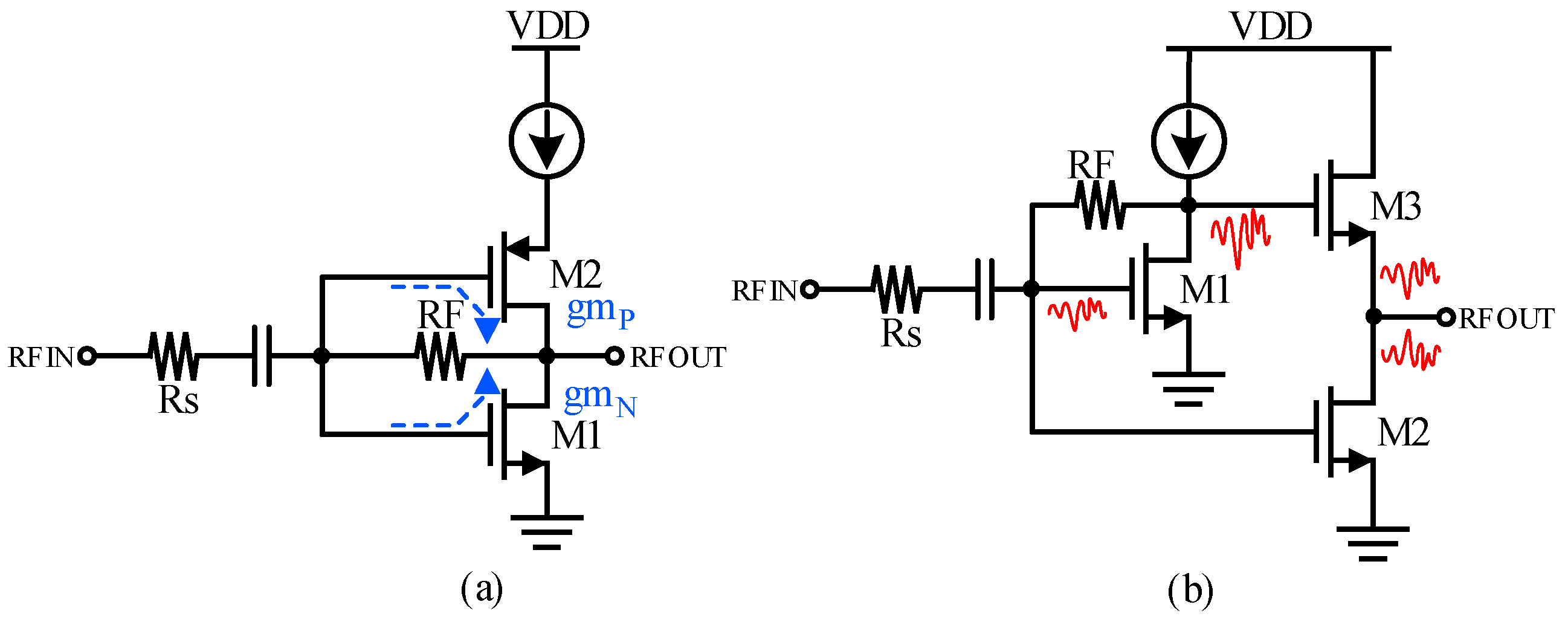
Figure 2.
Schematic of the proposed wideband LNA with values of its elements.
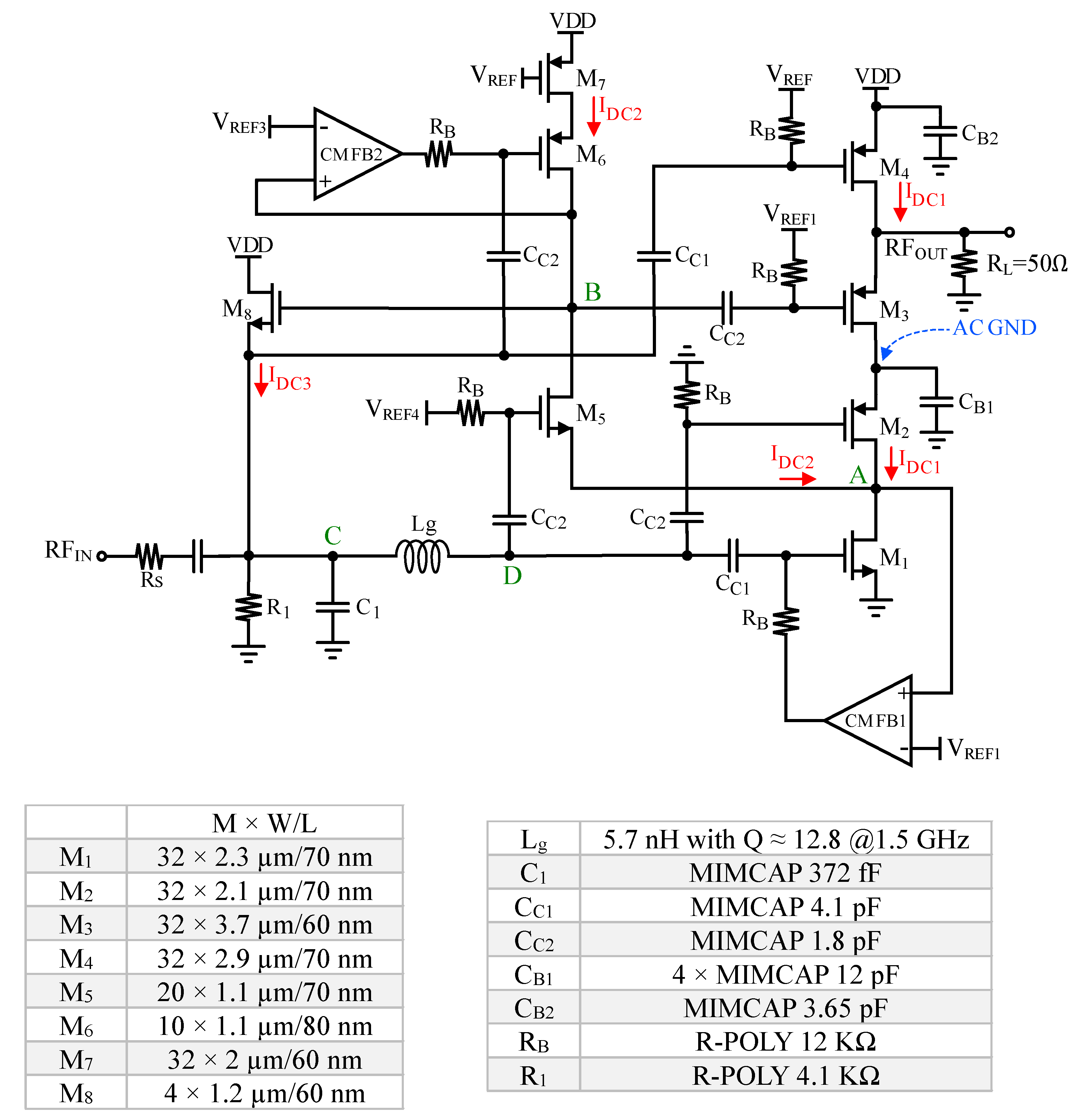
Figure 3.
Small signal model of first stage for input impedance calculation.
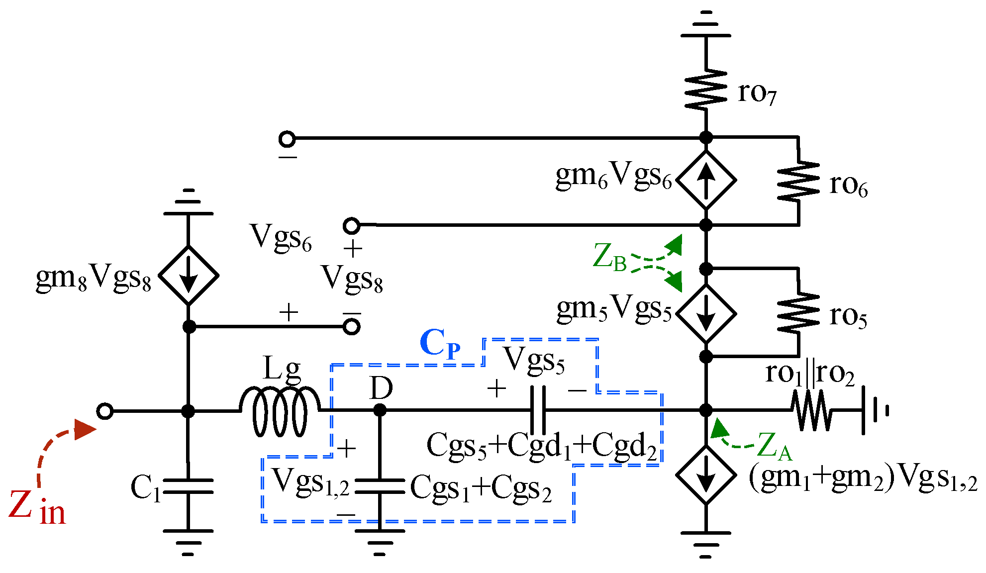
Figure 4.
AC model of the proposed LNA.
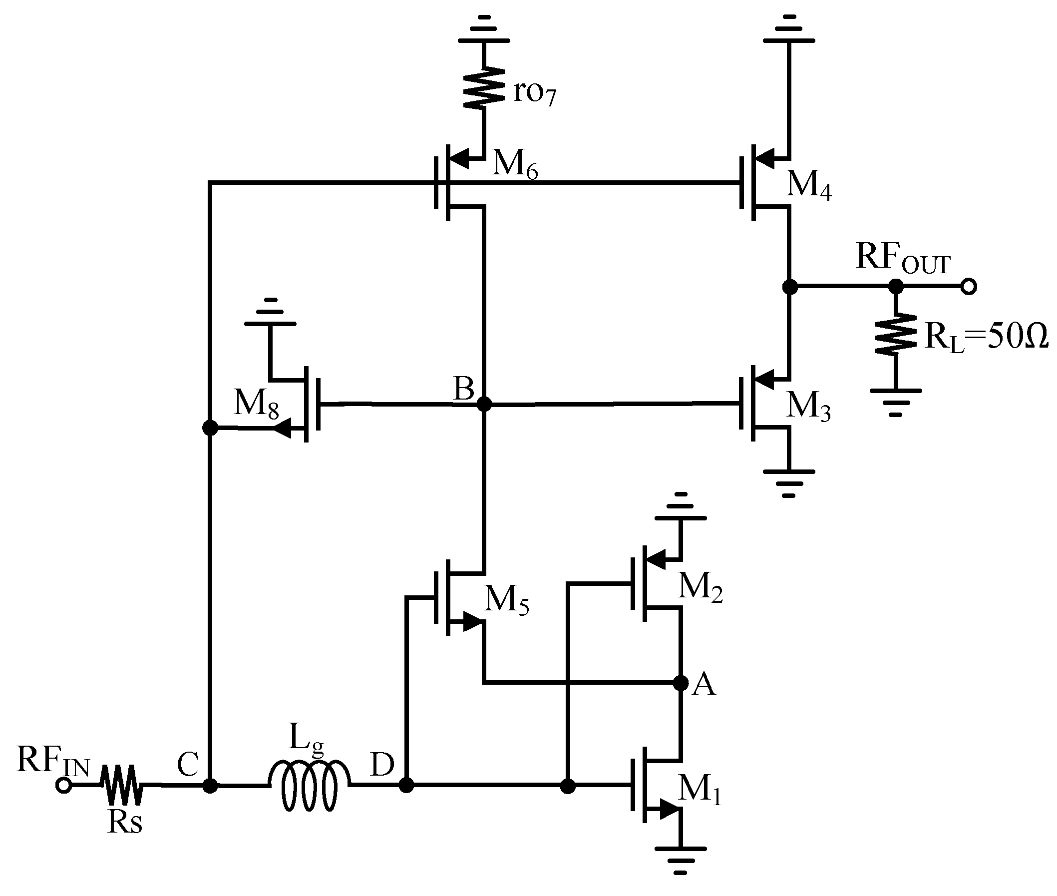
Figure 5.
Increasing 3dB bandwidth by using inductor Lg as series inductive peaking.
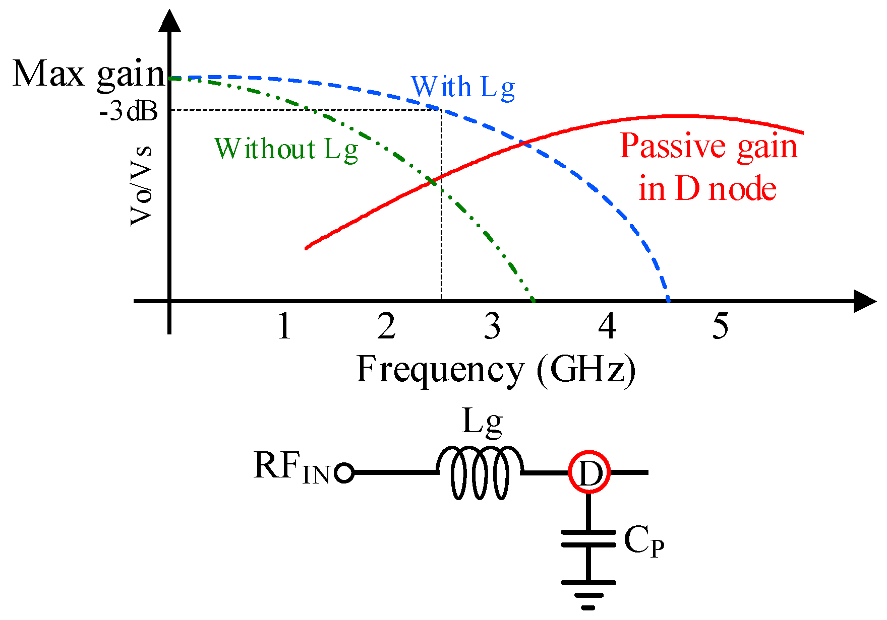
Figure 6.
The mechanism of the linearity improvement.
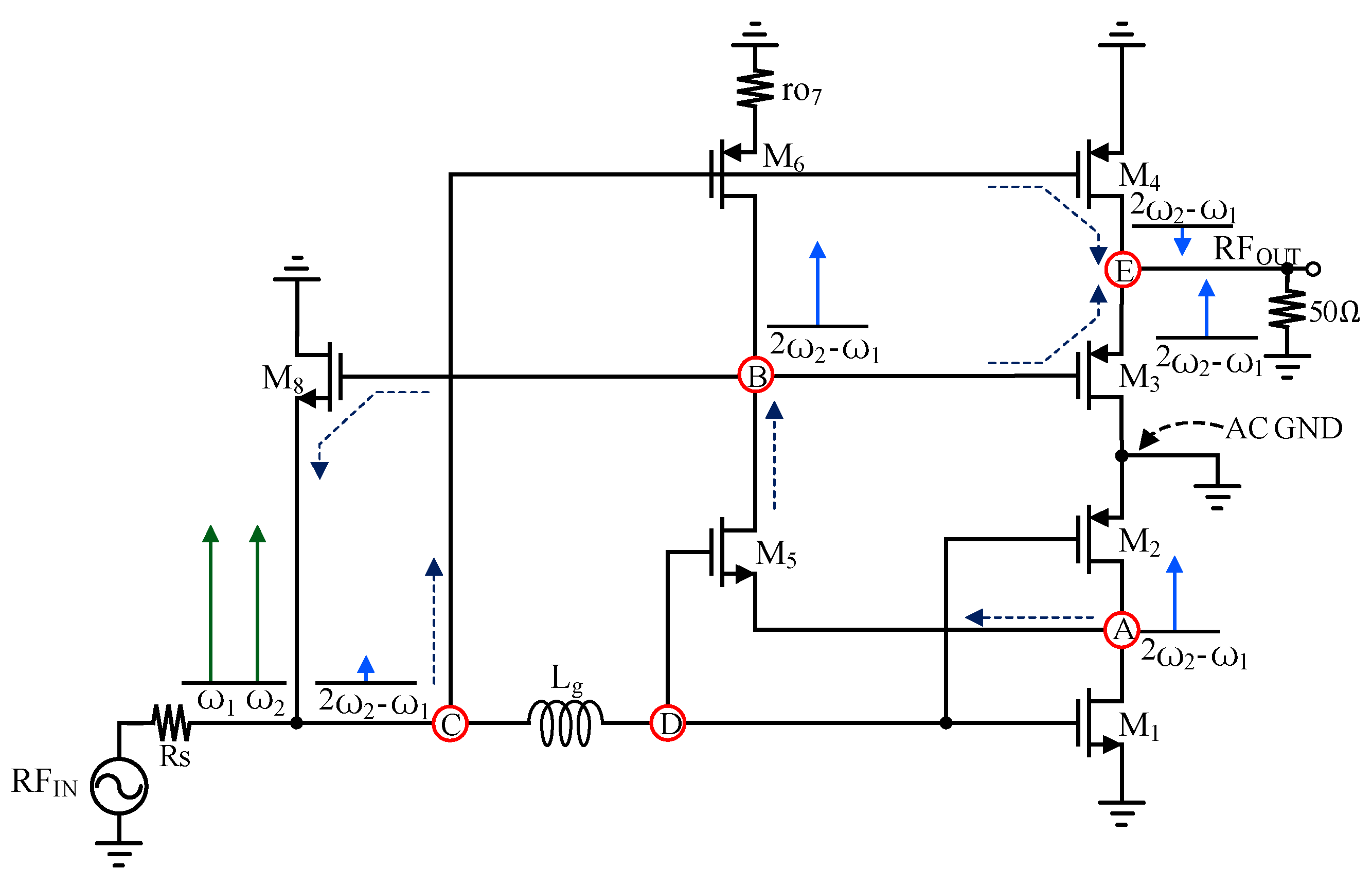
Figure 7.
The layout of the proposed wideband LNA with DC and signal PADs.
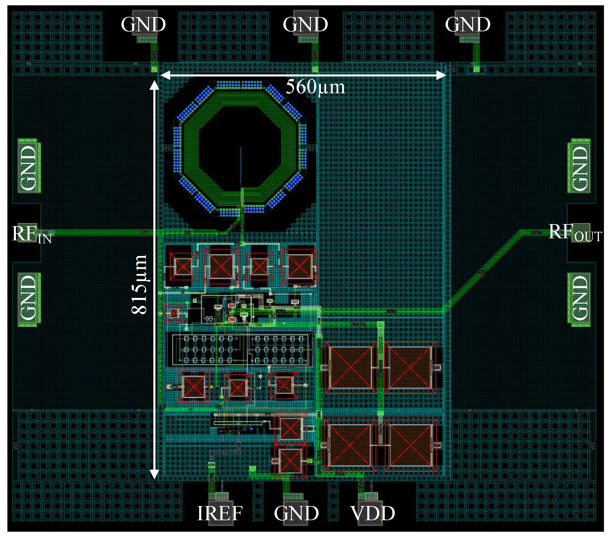
Figure 8.
(a) The post layout simulation of input and (b) output return losses in temperature and corner variations.
Figure 8.
(a) The post layout simulation of input and (b) output return losses in temperature and corner variations.
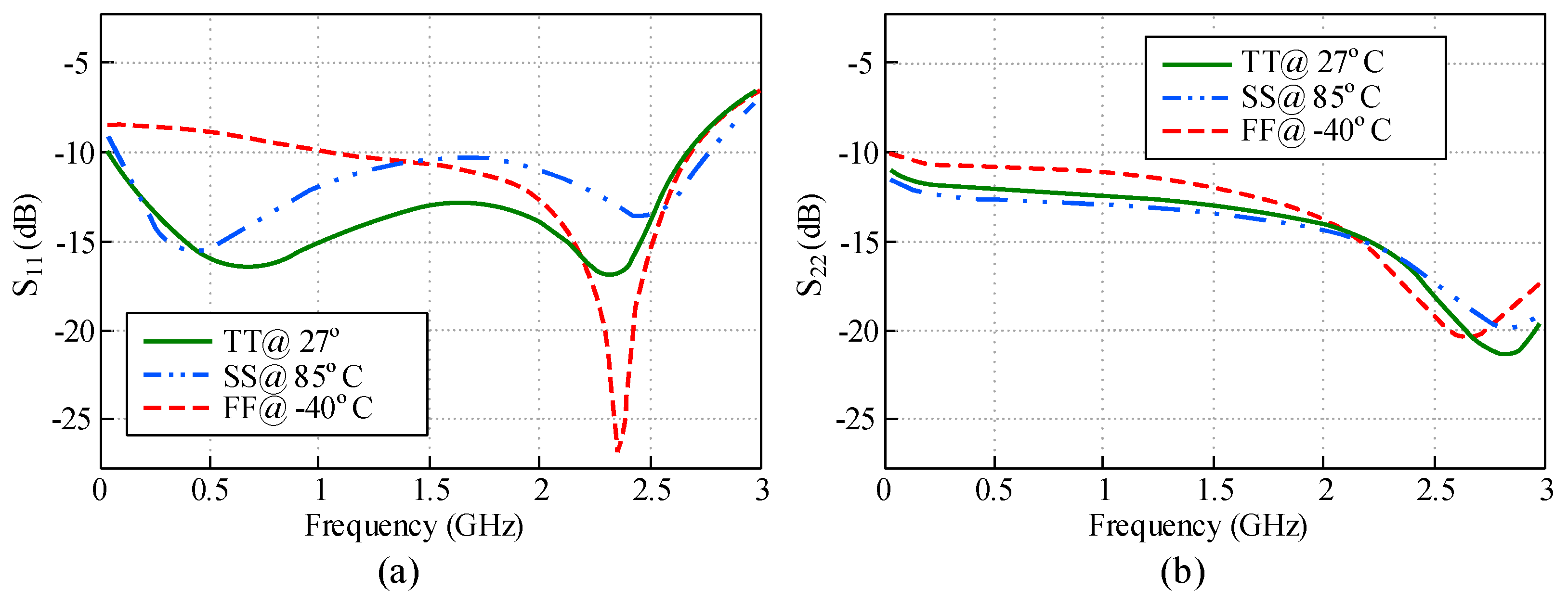
Figure 9.
(a) The post layout simulation of power gain and (b) NF in temperature and corner variations.
Figure 9.
(a) The post layout simulation of power gain and (b) NF in temperature and corner variations.
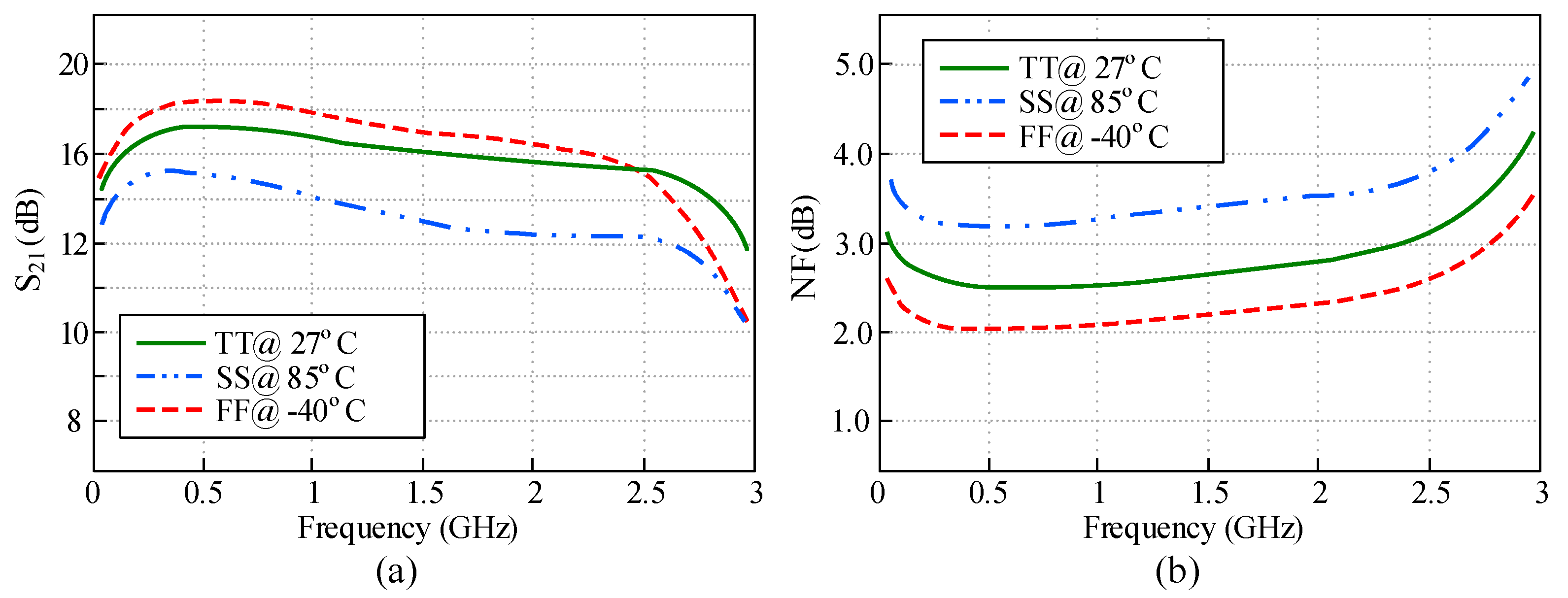
Figure 10.
Stability factor (Kf) from 0.1 to 12 GHz.
Figure 11.
Substrate map of 65 nm CMOS technology for EM simulation.

Figure 12.
(a) The inductor of Lg in ADS environment (b) inductance and Q-Factor of Lg by EM simulation.
Figure 12.
(a) The inductor of Lg in ADS environment (b) inductance and Q-Factor of Lg by EM simulation.
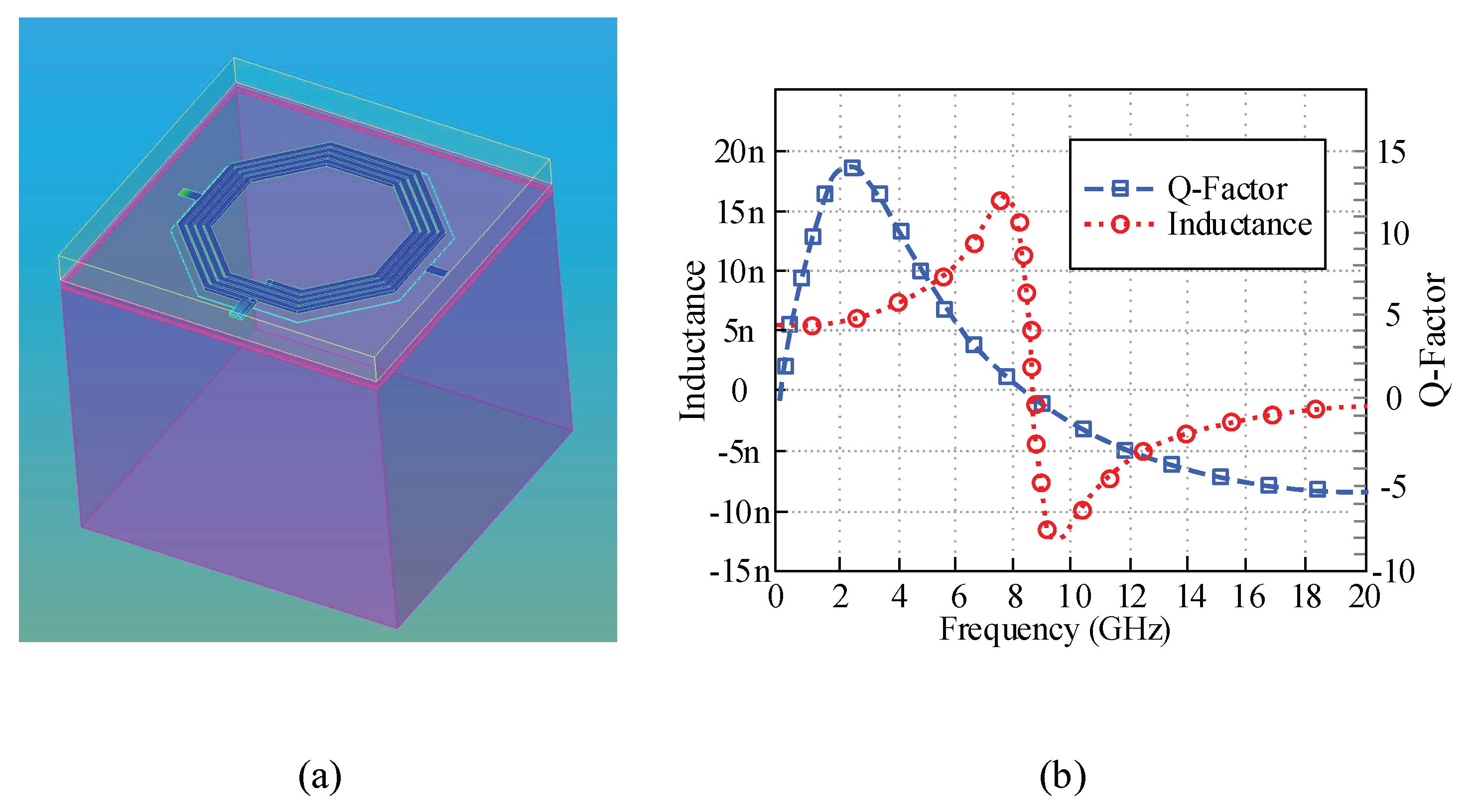
Figure 13.
(a) M4 as CS (b) M4 as a current source.
Figure 14.
(a) Amount of IIP3 at 2.4 GHz (b) IIP3 versus the input signal frequency with 10 MHz spacing.
Figure 14.
(a) Amount of IIP3 at 2.4 GHz (b) IIP3 versus the input signal frequency with 10 MHz spacing.
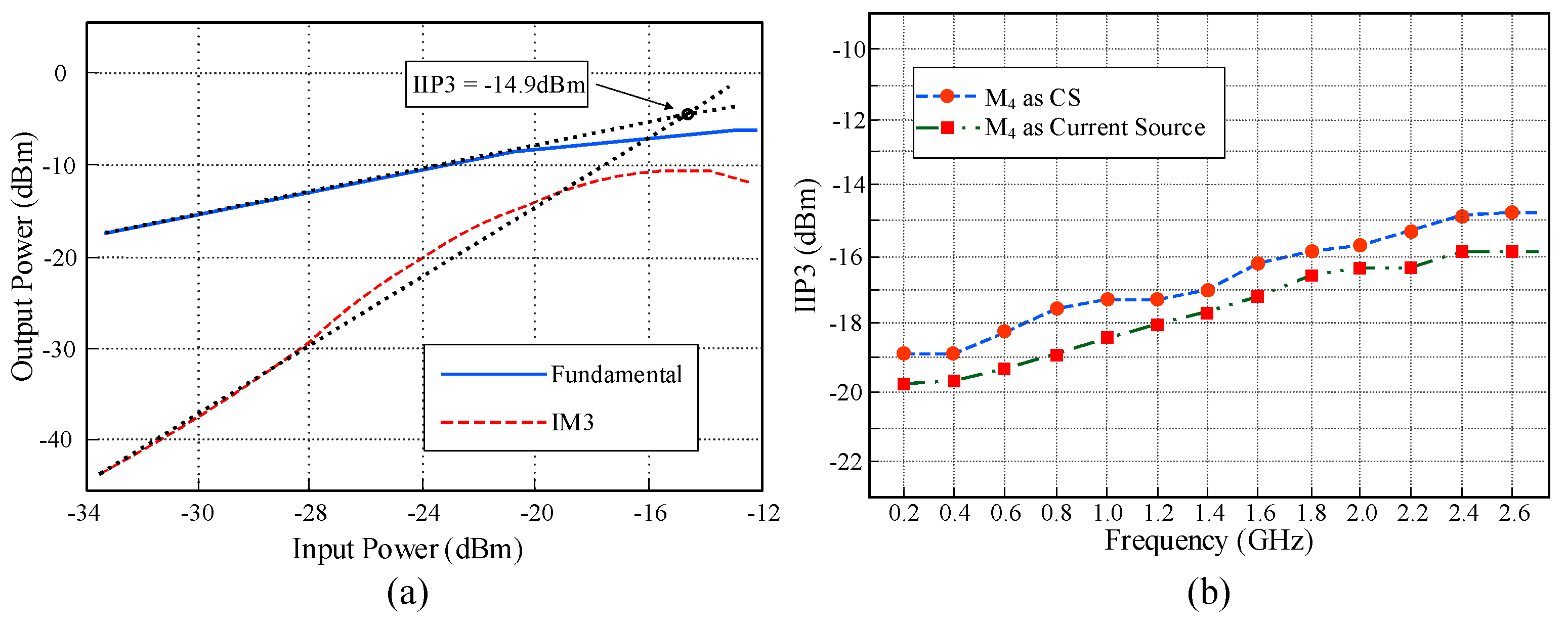

Table 1.
Corners and Temperature Simulation Results.
| Parameter | TT @ 27˚C | SS @ 85˚C | FF @ -40˚C |
|---|---|---|---|
| BW-3dB (GHz) | 0.17-2.68 | 0.17-2.2 | 0.17-2.54 |
| S21 (dB) | 15-17.24 | 13.58-15.58 | 15.2-18.2 |
| NFmin (dB) | 2.67 | 3.35 | 1.99 |
| IIP3 (dBm) | -14.9 | -13 | -12.6 |
| Power (mW) | 3.52 | 3.64 | 2.87 |
Table 2.
Performance Comparison with Several Recent Similar Works.
| Reference | CMOS Process | VDD (V) | Frequency (GHz) | S21 (dB) | NF (dB) | S11(dB) | IIP3(dBm) | Symmetric load | Power (mW) | Area (mm2) | FoM (dB) |
|---|---|---|---|---|---|---|---|---|---|---|---|
| TCAS-II’22*b [9] | 65 nm | 1.5 | 0.47-3.3 | 19.45-22 | 2.57-3.5 | <-10 | +2.81 | Yes | 12.5 | 0.057 | 11.02 |
| TCAS-I’19b [10] | 65 nm | 2.2 | 0.05-1 | 24-30 | 2.3-3.3 | <-12 | -4.1 | Yes | 19.8 | 0.045 | 6.84 |
| TCAS-I’20b [11] | 65 nm | 1 | 0.05-1.3 | 24-27.5 | 2.3-3 | <-12 | -2.2 | Yes | 5.7 | 0.046 | 17.73 |
| TCAS-II’21b [12] | 180 nm | 1.8 | 0.13-0.93 | 16.6-19.6 | 3.6-5 | <-10 | -8.5 | Yes | 3 | 0.18 | 6.52 |
| AEUE’19*b [13] | 180 nm | 1.2 | 0.18-2 | 15-20.8 | 2.65-3.8 | <-8 | -4.91 | Yes | 4.9 | 0.04 | 13.7 |
| TCAS-I’24b [14] | 65 nm | 0.78 | 0.1-4.2 | 15.6 | 4.45-6.9 | <-10 | -14.5 | No | 0.96 | 0.011 | 23.19 |
| MWT’25 [15] | 28 nm | 1.1 | 0.2-3.2 | 24.4-26 | 1.4-2.18 | <-15 | -3.6 | Yes | 17.4 | 0.018 | 19.13 |
| TCAS-I’24b [16] | 28 nm | 0.6 | 0.2-2.85 | 20 | 2.9-3.6 | <-13 | -12.3 | No | 1.74 | 0.0048 | 24.19 |
| TCAS-II’25b [17] | 130 nm | 1.3 | 0.01-1.7 | 21.5 | 1.1-1.9 | <-10 | -2.3 | Yes | 9.1 | 0.18 | 17.45 |
| This work* | 65 nm | 1 | 0.17-2.68 | 15-17.24 | 2.67-3.24 | <-10 | -14.9 | No | 3.52 | 0.45 | 15.7 |
* Post-layout simulation results. b needs buffer to measure.
Disclaimer/Publisher’s Note: The statements, opinions and data contained in all publications are solely those of the individual author(s) and contributor(s) and not of MDPI and/or the editor(s). MDPI and/or the editor(s) disclaim responsibility for any injury to people or property resulting from any ideas, methods, instructions or products referred to in the content. |
© 2025 by the authors. Licensee MDPI, Basel, Switzerland. This article is an open access article distributed under the terms and conditions of the Creative Commons Attribution (CC BY) license (http://creativecommons.org/licenses/by/4.0/).
Copyright: This open access article is published under a Creative Commons CC BY 4.0 license, which permit the free download, distribution, and reuse, provided that the author and preprint are cited in any reuse.


