
Submitted:
07 October 2025
Posted:
09 October 2025
You are already at the latest version
Abstract
In this study, we present the design and analysis of a stacked inverter-based 1
millimeter-wave (mmWave) power amplifier (PA) in 90nm CMOS targeting wideband Q-band operation. The PA employs two PMOS and two NMOS devices in a fully stacked inverter topology to distribute device stress, remove the need for an RF choke, and increase effective transconductance while preserving compact layout. A resistor ladder biases thestack near VDD/4 per device, and capacitive division steers intermediate-node swings to enable class-E-like voltage shaping at the output. Closed-form models are developed for gain, output power, drain efficiency/PAE, and linearity, alongside a small-signal stacked-ladder formulation that quantifies stress sharing and the impedance presented to the matching networks; L/T network synthesis relations are provided to co-optimize bandwidth and insertion loss. Post-layout simulation in 90nm CMOS shows |S21| = 10 dB at 39.84GHz with 3 dB bandwidth from 36.8–42.4 GHz, peak PAE of 18.38% near 41 GHz, and saturated output power Psat = 8.67dBm at VDD = 4V, with S11 < −15 dB and reverse isolation ≈ −16 dB. The layout occupies 1.6×1.6mm2 and draws 31.08mW. Robustness is validated via a 200-run Monte Carlo showing tight clustering of Psat and PAE, sensitivity sweeps identifying sizing/tolerance trade-offs (±10% devices/passives), and EM co-simulation of on-chip passives indicating only minor loss/shift relative to schematic while preserving the target bandwidth and efficiency. The results demonstrate a balanced gain–efficiency–power trade-off with layout-aware resilience, positioning stacked-inverter CMOS PAs as a power and area-efficient solution for mmWave front-ends.
Keywords:
mmWave
; power amplifier
; stacked inverter
; CMOS
; Q-band
; PAE
; Monte Carlo
; EM co-simulation
; matching networks
1. Introduction
The rapid evolution of wireless communication technologies has brought millimeter-wave (mmWave) systems to the forefront of modern research, particularly for applications such as wideband wireless communication, satellite radio, and automotive radar. These advancements are driven by the need for higher data rates, improved spectral efficiency, and compact system integration. Among the critical building blocks, power amplifiers (PAs) play a central role as the final stage of the transmitter chain, providing the required output power to the antenna. The development of efficient mmWave PAs has therefore become a focal point of ongoing research, with complementary metal-oxide-semiconductor (CMOS) technology emerging as a promising candidate due to its low cost, small footprint, and compatibility with on-chip integration [1].
Despite these advantages, the design of high-power and efficient CMOS PAs at mmWave frequencies remains challenging. CMOS devices suffer from limited breakdown voltage, high knee voltage, and reduced gain, along with poor-quality on-chip passive components. In advanced technology nodes, issues such as gate oxide breakdown and hot-carrier effects further constrain achievable output power and long-term reliability [2,3,4]. These challenges necessitate innovative circuit techniques to meet the stringent requirements of mmWave front-ends.
One major consideration is the design of output matching networks that transform the inherently low impedance of CMOS transistors to the standard antenna load. While device scaling and transistor sizing can increase drain current to boost output power, this approach lowers input impedance, making impedance matching more complex [5,6,7]. Achieving watt-level output often requires large impedance transformations, which can introduce additional losses and reduce efficiency. In portable applications, where the PA is a dominant power consumer, improving efficiency is critical for extending battery life and enhancing overall system performance [8,9,10].
Several CMOS PA architectures have been explored to address these challenges. Cascode amplifiers provide high gain and isolation but suffer from limited voltage headroom in scaled processes [7,8]. Doherty amplifiers improve back-off efficiency for modulated signals, yet their implementation in nanoscale CMOS is hindered by parasitics and complex matching requirements [9]. Distributed amplifiers offer wide bandwidth but typically consume large silicon area and achieve relatively low peak power-added efficiency (PAE) [17]. These trade-offs have motivated alternative approaches such as inverter-based stacked topologies, which distribute voltage stress across devices, eliminate bulky RF chokes, and simplify integration [6,12].
Progress in CMOS PA design across technology nodes reflects steady innovation. Sowlati and Leenaerts [7] demonstrated a 2.4 GHz cascode PA in 180 nm CMOS with modest efficiency, while Huang [13] presented a 60 GHz distributed PA in 90 nm CMOS that achieved wideband performance but low PAE. Barton [14] explored Doherty architectures at 28 GHz in 130 nm CMOS with improved back-off efficiency, whereas Son et al. [6] introduced a stacked n/pMOS PA at 1.8 GHz in 180 nm CMOS. Kiumarsi et al. [12] further advanced inverter-stacked PAs in 65 nm CMOS, highlighting their potential despite efficiency constraints.
More recent work has pushed the limits of CMOS PAs. Chakrabarti and Krishnaswamy [15] reported a 45 nm SOI stacked Class-E-like PA at 45 GHz achieving a peak PAE of 34.6% with of 17.6 dBm in a two-stack configuration, and 19.4% PAE with of 20.3 dBm in a four-stack version. Ogunnika and Valdes-Garcia [20] demonstrated a 32 nm SOI Class-E tuned PA at 60 GHz with nearly 30% PAE. At 29.5 GHz, Oulu University researchers [23] designed a dual-input stacked PA in 22 nm FD-SOI, achieving 11.5 dB gain, 19.5 dBm , and 17% PAE. A GlobalFoundries 22FDX® 28 GHz dual-stage PA reported peak PAE of 31.5%, while Mayeda et al. [24] showcased a broadband PA covering 24–43.5 GHz in 22 nm FD-SOI. Most recently, Yamamoto et al. [25] demonstrated a 28 nm CMOS D-band PA operating from 110–170 GHz with 7.6% PAE, illustrating ongoing efforts to extend CMOS PA performance into higher frequency ranges.
Together, these prior works highlight both the advances and persistent limitations of CMOS PA design across architectures, technology nodes, and frequency bands. The stacked-inverter PA proposed in this work leverages inverter-based gain enhancement and transistor stacking to overcome voltage stress limitations, improve efficiency, and simplify circuit integration. By combining these benefits, the design achieves a balanced trade-off among gain, output power, and efficiency, making it a strong candidate for high-performance mmWave communication systems [11,12]. One effective approach is the use of stacking of multiple transistors to form a composite structure which allows the power amplifier (PA) to handle higher voltage swings by distributing voltage stress across the devices, thereby reducing the risk of breakdown. It also facilities impedance matching and enables higher output power supporting wideband performance. All of these advantages make the stacked configuration especially suitable for mmWave applications, where high data rates and spectral efficiency are essential.
The main aim of this work is to design and analyze a stacked-FET power amplifier (PA) using four transistors in a 90 nm CMOS process, with a particular focus on optimizing impedance matching among the stacked devices. This optimization is critical for enhancing output power, power-added efficiency (PAE), and bandwidth—key parameters for mmWave communication systems. The stacked configuration effectively reduces CMOS technology’s inherent limitations such as low voltage handling and thermal stress. The design lowers the possibility of thermal runaway and increases device reliability by dividing the voltage and thermal load among several transistors. Optimizing on-chip passive components (such as inductors and capacitors) also helps to maintain a high Q-factor and reduce losses. Overall, the proposed design demonstrates strong potential for high-efficiency mmWave power amplifiers in modern wireless systems.
In this paper, we present an analysis of a stacked-FET power amplifier (PA) using four transistors in CMOS technology, with a particular focus on the impedance matching between the stacked transistors. Finally, we demonstrate the performance of a wideband power amplifier with four stacked FETs implemented in a 90nm CMOS process. The combination of output power and efficiency achieved for CMOS-based amplifiers, making it suitable for mmWave and wideband applications.
2. Modeling and Design of Choke-Less Inverter-Based Stacked PA
2.1. Choke-Less Inverter-Based PA: Splitting Stress and Combining for Wideband Gain
In conventional Class-E power amplifiers, a single switching device experiences a high peak VDS whereas signal swing is twice the supply voltage and hence voltage stress is 2VDD across its VDS., which can exceed the breakdown voltage of CMOS transistors, particularly in handset applications where the supply voltage is typically 3.3V or higher[12]. The proposed design introduces an additional switching device to split the output voltage swing between the drain nodes of NMOS and PMOS transistors in which VDS will be at most VDD , eliminating the need for a choke inductor and simplifying the amplifier structure. Instead of reducing VDD , the proposed Inverter-based amplifier lowers the drain-source voltage of each active device compared to a conventional Class-E amplifier operating at the same supply voltage[15]. The conventional PA has the gain that depends only on NMOS transconductance. But in inverter-based amplifier has NMOS and PMOS transconductances combined, resulting in higher effective gm and greater voltage gain[21]. In addition, the inverter also lacks internal nodes, which means there are no additional poles or zeros. This allows it to maintain better frequency response and bandwidth than that of the conventional common-source amplifier especially at high frequencies[22].
2.2. Modeling of Transistors, Capacitors, and Bias Resistors for Intermediate-Node Matching and Balanced
In a stacked configuration, multiple transistors are in series; only the bottom device is directly driven to preserve input power and enhance PAE. Upper-stack devices switch due to intermediary node swings, while the top drain sustains a class-E-like waveform, ensuring balanced voltage stress across all devices. For reliability, the voltage swing between transistor junctions must not exceed 2VDD, resulting in a peak output swing of 2VDD for an n-stack PA[10].
Intermediary node voltage swing can be achieved using techniques like capacitive charging acceleration[6].To maintain the peak AC swing limit across the gate-source junction in the on half-cycle and the gate-drain junction in the off half-cycle. The swing at gate voltages in the stack is induced through capacitive coupling via () and (), which are controlled by the gate capacitor [8].Capacitors also adjust the impedance at each drain node, which ensures that each transistor operates at its optimum impedance for maximum power delivery. A resistive ladder from the drain to the gate of the topmost FET used for DC biasing ensures maximum voltage swing at the output. Without the feedback mechanism, the gate voltages of the stacked FETs remain zero and do not turn on while their source voltages vary under RF power conditions. This mismatch could cause early device breakdown due to gate-source voltage limitations, reducing power output.
Load impedances at intermediate nodes of the stack have a significant reactive component at mm-wave frequencies due to transistor and interconnect capacitances. The reactive component of the node impedance reduces efficiency by (a) causing part of the transistor RF current to flow through () and other capacitances instead of reaching the load and (b) disrupting the phase alignment of voltage waveforms at the transistor drains, reducing the top drain’s voltage swing. To achieve proper matching at intermediate nodes, passive elements, such as series inductance can be used[11].
2.3. Design of the Proposed Stacked PA Architecture
Most stacked PAs described so far rely entirely on NMOS transistors, except for the design by Son et al [6]. While their PA includes both NMOS and PMOS transistors, it doesn’t fully adopt a stacked structure. Instead, only two transistors—either NMOS or PMOS—are stacked, and a transformer is used to merge their output power. In this study, we use a new strategy from the conventional CMOS inverter design by fully stacking NMOS and PMOS devices. Our method expands on the self-biased cascode technique by increasing efficiency and power management, making it a promising choice for upcoming applications [12]. An inverter-based stacked PA composed of two NMOS and two PMOS transistors is shown in Figure 1.
In our design, we used a stacked inverter-based booster that incorporates two vertically stacked inverters, utilizing two thin-oxide PMOS and two NMOS transistors, capable of achieving output swings . In SOI CMOS process, each MOSFET is fully isolated by shallow trench isolation regions and a buried oxide layer, allowing for effective isolation even at DC and supporting voltages up to 10 V. In our design, the drain-source (), gate-source (), and gate-drain ( voltages for each transistor are kept within the maximum supply voltage of 1.1 V. In the booster design, the dimensions of the upper MOSFETs in the stack are gradually reduced, as they experience smaller current swings. This minimizes output capacitance and enhances the output stage’s bandwidth and output power. Additionally, capacitors are placed between the gates of the MOSFETs and ground to create a capacitive voltage divider with the gate-source () and drain-gate () capacitances of their respective MOSFETs using (1).
This configuration ensures that a larger fraction of the input voltage signal is presented at the gate of the MOSFETs located higher up in the stack, such a way that voltage swings across each transistor in the stack will add up in phase at the output node.The appropriate DC bias gate voltage for the stacked MOSFETs is established via a resistive divider, ensuring that each transistor experiences a drain-source voltage () of approximately /4. Resistor values were calculated accordingly, with minor adjustments made in the final design to balance power consumption and load matching.
Furthermore, the output stage’s high-frequency performance is improved by adjusted MOSFET finger width and gate finger count. The input matching network is designed to convert the system impedance to the transistor’s input impedance, ensuring maximum power transfer and gain enhancement [6]. The T-network was chosen for its ability to match a wide range of impedances, consisting of two shunt capacitors and and one series inductor .Similarly, the output matching network transforms the transistor’s output impedance to , optimizing both gain and stability of the power amplifier through a low-pass matching network, which consists of a series inductor followed by a capacitor .
To verify the large-signal behavior of the proposed stacked inverter-based power amplifier, a transient simulation was performed . The schematic of the designed circuit is shown in Figure 2(a) . A 1 sinusoidal signal at operating frequency was applied at the input. The transient waveforms of the input signal, output signal, and the intermediate node voltages and are shown in Figure 2(b).From the waveforms, it can be observed that the input signal is properly amplified at the output, indicating that the amplifier operates as expected under large-signal excitation.
2.4. Analytical Modeling and Design Equations
2.4.1. PA Gain, Output Power, Efficiency, and Linearity
For a matched load at , the large-signal fundamental output power is
where and are the fundamental components of the output voltage and current, respectively. In small-signal, the midband power gain can be approximated as
with the effective transconductance driving the load seen by the PA core, and the real part of the transformed load at the PA output node.
The power-added efficiency (PAE) and drain efficiency (DE) follow
where is the RF input power and . The saturated output power is the maximum before hard clipping (or at the knee of the vs. curve); practically, it is extracted from large-signal simulations/measurements at the onset of saturation.
A memoryless weakly nonlinear baseband model,
captures AM/AM nonlinearity. The input-referred third-order intercept point is
and the 1 dB compression point occurs where the small-signal gain drops by 1 dB relative to . In practice, and (O/I)IP3 are obtained from PSS/PAC and two-tone simulations consistent with Fig. 4–5 of this work.
2.4.2. Small-Signal Model of the Stacked Inverter: Stress Sharing and Impedance
An inverter-based unit provides an additive transconductance
while its small-signal output resistance satisfies
For an N-device voltage stack (alternating p/n devices as in this work), a first-order small-signal stress-sharing model assumes a capacitive divider between adjacent device nodes. Denote the intrinsic capacitances of device k by and and any intentional gate capacitors by ; the interstage voltage division yields
where the tridiagonal matrix collects node-to-node capacitances () and are frequency-dependent division ratios. The device peak stress is then
with a small imbalance term due to parasitics/mismatch. In this design, biasing targets per device for a 4-stack, consistent with the post-layout operating points and the divider expression used in (1) of the manuscript. (See Sec. 2 and Tables 1–2 for device stresses and the capacitor-divider choice.) :contentReference[oaicite:0]index=0
The inverter stack’s effective driving transconductance to the top node can be expressed as
where captures the attenuation across the stacked ladder (set by and device ). The load seen by the top node is the transformed :
and enters (3).
2.4.3. Input/Output Matching Networks (L and T) at
For an L-match between real resistances and at center frequency :
Case A: (series , shunt at the load).
Choose reactances as inductive/capacitive per topology (high-pass or low-pass). Convert to parts via , .
Case B: (series , shunt at the source).
For a T-network (all-reactive, real ), selecting a desired loaded quality factor gives the series and shunt reactances
The three reactances are then implemented as series and a shunt at . For band-edge shaping or realizability with on-chip passives, one can sweep to trade off insertion loss (hence PAE) against bandwidth. The same synthesis applies to the input network by substituting the source impedance (usually ) and the PA input resistance/capacitance (dominated by in (7) and ).
2.4.4. Putting It Together
3. Physical Implementation and Post-Layout Characterization of the Proposed Design
3.1. Layout
The layout of the stacked inverter-based power amplifier shown in Figure 3 is designed using 90nm CMOS technology, occupying a chip area of 1.6mm × 1.6mm. This design optimizes metal routing and transistor placement which ensure minimal parasitic effects and efficient power distribution. Also multilayer metal interconnects were used to handle high current flow, and careful ground planning was applied to reduce inductive noise. The power amplifier consumes 31.08mW, demonstrating low-power operation.
3.2. Post-Layout Simulation Results
The results section contains DC simulated schematic illustrating the operating points of all transistors in Figure 4. Additionally,Table 1 lists each transistor’s , , and along with in Table 2 the specific currents flowing through the parallel resistors is included. This confirms that every device operates within the 1.2 V safe breakdown threshold. Furthermore, the analysis verifies that the circuit performs reliably and effectively within the specified parameters.
The simulated small-signal scattering parameters (S parameters) of the power amplifier (PA) using Cadence spectre simulator are presented in Figure 5(a) and (b).The designed PA achieves a gain of 10 dB at a center frequency of 39.84 GHz, which is ideal for mmWave uses calling for high-frequency operation.The 3 dB bandwidth extends over 7 GHz, from 36 GHz to 43 GHz, this bandwidth especially beneficial for wideband communication systems since high data rate transmission depends on maintaining constant gain across a large spectrum. The PA is a good option for applications requiring reliable signal amplification and spectral efficiency due to its gain and bandwidth characteristics.
In RF systems, effective impedance matching is essential to ensure maximum power transfer and minimize signal reflections, thereby improving overall performance and efficiency. The input of the PA is well matched to 50 Ω with S11 of less than -15dB across the operating bandwidth. This low S11 value signifies minimal signal reflection at the input, ensuring efficient coupling of the input signal into the amplifier. A reverse isolation (S12) of -16 dB indicates that there is minimal signal leakage from the output port back to the input port in the power amplifier design, which helps maintain signal integrity and stability. Linearity is an important parameter in PA design, alongside gain. It determines the maximum usable output power that the PA can deliver to the load. To evaluate linearity, periodic steady-state (PSS) analysis is typically used in simulations. As can be seen from Figure 6(a) and (b) input and output referred 1-dB compression point of -7.20826 dBm and 1.80812 dBm respectively, is obtained at frequency of 39.84 GHz.
The input third order inter-modulation IIP3 of 14.54 dBm is obtained at 4.73 dBm input power in Figure 7. Since mmWave systems demand high power levels, power-added efficiency (PAE) and output power are critical parameters for assessing the performance of a power amplifier (PA). Figure 8 shows the measured output power and power-added efficiency (PAE) over a frequency band of 36-46 GHz at a supply voltage of 4V. The power-added efficiency of the PA peaks at 18.38% at 41GHz. The saturated output power () reaches 8.67 dBm, proving that the PA can provide enough power for mmWave applications.
3.3. Quantifying Robustness Under Mismatch: MC/Sensitivity/EM Results
In addition to the baseline results, we performed statistical and layout-aware evaluations to quantify robustness and to isolate the impact of on-chip passives. A 200-point Monte Carlo (MC) campaign incorporating threshold, mobility, and passive-variation corners shows that both and PAE remain tightly clustered about their nominal values, indicating adequate variance immunity for the stacked-inverter core and its matching networks. The PAE distribution in Figure 9(a) is approximately Gaussian with a narrow spread, while the histogram in Figure 9(b) exhibits similar concentration, reflecting stable large-signal swing and load transformation across mismatch realizations. To quantify design levers, we conducted local sensitivity sweeps. Transistor width scaling (Figure 10) shows that enlarging the unit devices increases and improves monotically (beneficial for in (2)), but degrades PAE due to higher parasitic charging loss and diminished leverage in (3); this sets an upper bound on practical sizing before efficiency roll-off dominates. Inductor tolerance (Figure 11) and capacitor tolerance (Figure 12) each perturb the matching Q and resonant frequency, producing predictable shifts in peak response and small reductions in efficiency/output power; these trends match the L/T-network relations in (13)–(16) and confirm that modest guard-bands ( passives) keep performance within spec without overconstraining on-chip passive design rules. The MC scatter plot in Figure 13(a) reveals a weak anti-correlation between PAE and : realizations that slightly favor load-line swing (marginally higher ) tend to incur a modest efficiency penalty due to increased device conduction and reactive loss, consistent with the power balance in (4) and the gain dependence in (3). Finally, EM co-simulation of inductors and critical interconnects (Figure 13) shows a slight downshift in the passband and a small insertion-loss increase (finite inductor Q and weak mutual coupling), yet post-EM tracks the schematic shape closely and preserves the targeted bandwidth and efficiency envelope, validating the stress-sharing assumption in (10) and the effective transconductance transfer in (11). Taken together, the MC, sensitivity, and EM overlays indicate that (i) the stacked ladder’s voltage division and impedance transformation are tolerant to local mismatch, (ii) device sizing should be capped by the PAE turning point identified by the width sweep, and (iii) first-order L/T designs remain accurate after EM back-annotation, requiring only minor retuning of the matching reactances for tape-out.
The performance of the proposed CMOS power amplifier, as shown in Table 3, outperforms many earlier studies at comparable frequencies with a good balance of gain, bandwidth, and power-added efficiency. Against recent FD-SOI mmWave exemplars (22 nm, 29.5 GHz dual-input stacked PA; and a 22 nm broadband PA covering 24–43.5 GHz) [23,24], the proposed bulk-90 nm design trades absolute power/gain for process accessibility, area compactness (1.6×1.6 mm2), and layout-aware robustness (Monte Carlo, sensitivity, EM co-sim), while retaining competitive PAE for its node and complexity. Conventional Class-E PAs concentrate a swing across a single device, stressing [12,15]; in contrast, the choke-less stacked-inverter core redistributes voltage and raises effective drive via combined NMOS/PMOS [11,21,22], with capacitive charging acceleration and intermediate-node matching stabilizing stress and bandwidth [6,8,11].
4. Discussion
This work demonstrated a choke-less, inverter-stacked PA in 90 nm CMOS for mmWave operation with dB at 39.84 GHz and a 3 dB bandwidth of 36.8–42.4 GHz, achieving peak PAE of 18.38% at 41 GHz and dBm at V. While these results confirm efficient power utilization and broadband matching, several factors bound ultimate performance. The PAE ceiling at Q-band is constrained by device knee/conduction losses, incomplete harmonic terminations, and finite on-chip passive Q; even carefully synthesized L/T networks incur metal and substrate loss that limits drain efficiency and back-off PAE. Thermal reliability also becomes critical at mmWave: self-heating degrades and , shifts bias, and narrows the safe operating area, while EM/IR drop and current crowding cap sustainable output power. Finally, stacking complexity imposes practical overhead—intermediate-node impedances are partly reactive, so any mismatch increases circulating current and phase error, reducing the top-node swing; robust operation therefore requires tightly tuned gate capacitors and bias ladders to keep within limits across PVT, along with start-up biasing that avoids latch-up or over-voltage.
Looking forward, several directions can raise linearity, efficiency, and integration readiness. Linearity can be improved via digital predistortion (DPD) tailored to FR2 EVM/ACLR masks, envelope/rail tracking aligned with stacked-inverter dynamics, and selective analog techniques (adaptive bias, light degeneration, neutralization) that mitigate AM/AM and AM/PM with modest PAE cost; co-optimizing bias and matching with two-tone/IP3 and PSS/PAC analyses tightens the –PAE trade. Architectural scaling with a modest-gain driver relaxes the main stage’s input impedance target, enabling a slightly higher load line and improved ; asymmetric device sizing or gate-capacitor tapering across the stack can refine stress sharing and reduce dynamic loss. Migration to SOI/FD-SOI (22–45 nm) promises higher effective breakdown, lower substrate loss, and better isolation for passives and interconnects, typically lifting PAE and easing EM closure. Finally, integrating compact on-chip baluns or magnetically coupled lines enables differential drive/combining and simplifies antenna co-integration; EM-first co-design of spirals and transmission lines, with metal-density-aware ground grids and coupling management, can raise passive Q, reduce mismatch sensitivity, and stabilize phase across intermediate nodes.
Overall, the presented 90 nm design establishes a solid baseline for stacked-inverter mmWave PAs—broadband gain, competitive PAE, and layout-aware robustness—while clarifying the remaining gaps to state of the art. Closing those gaps will require simultaneously lowering passive and dynamic loss to lift the PAE ceiling, applying thermally aware floorplanning and power-grid design to sustain higher , and combining driver stages, load-modulation strategies, SOI migration, and EM-first passive/balun co-design. These steps provide a concrete path to higher back-off efficiency, improved linearity for high-order QAM, and resilient tape-out in advanced nodes.
5. Conclusions
This work presented a choke-less, inverter-stacked millimeter-wave PA in 90 nm CMOS that demonstrates a balanced gain–efficiency–power trade-off with layout-aware robustness. The fully stacked inverter core (two PMOS + two NMOS) distributes device stress to constrain per-device , eliminates the RF choke, and combines NMOS/PMOS transconductances for strong midband drive. Guided by closed-form models for gain, output power, PAE, and linearity, as well as small-signal ladder analysis for stress sharing and impedance transformation, the design employs L/T network synthesis to co-optimize bandwidth and insertion loss. Post-layout simulations show dB at 39.84 GHz with 3 dB bandwidth from 36.8–42.4 GHz, peak PAE of 18.38% near 41 GHz, and dBm at V, while maintaining dB and reverse isolation dB. The implementation occupies mm2 and draws 31.08 mW. Robustness was validated through a 200-run Monte Carlo (tight clustering of and PAE), device/passive sensitivity sweeps (predictable sizing/tolerance trade-offs), and EM co-simulation (minor post-EM loss/shift with preserved bandwidth), collectively confirming resilience to process/mismatch and physical parasitics. Overall, the results establish the stacked-inverter topology as a power- and area-efficient mmWave PA solution in bulk 90 nm CMOS, and provide a solid foundation for further gains via linearization, staged architectures, SOI/FD-SOI migration, and EM-first passive/balun co-design.
References
- Niknejad, A. M.; Chowdhury, D.; Chen, J. Design of CMOS power amplifiers. IEEE Transactions on Microwave Theory and Techniques 2012, 60, 1784–1796. [Google Scholar] [CrossRef]
- Bhale, V. M.; Shah, A. D.; Dalal, U. D. 3–5 GHz CMOS power amplifier design for ultra-wide-band application. In Proceedings of the International Conference on Electronics and Communication Systems (ICECS), Coimbatore, India, 13–14 February 2014; pp. 1–4. [Google Scholar] [CrossRef]
- Hsieh, C.-Y.; Kao, J.-C.; Kuo, J.-J.; Lin, K.-Y. A 57–64 GHz low-phase-variation variable-gain amplifier. In Proceedings of the IEEE/MTT-S International Microwave Symposium, Montreal, QC, Canada, 17–22 June 2012; pp. 1–3. [Google Scholar]
- Wang, T.-Y.; Lai, M.-R.; Twigg, C. M.; Peng, S.-Y. A fully reconfigurable low-noise biopotential sensing amplifier with 1.96 noise efficiency factor. IEEE Trans. Biomed. Circuits Syst. 2013, 8, 411–422. [Google Scholar] [CrossRef] [PubMed]
- Chen, W.-M.; Chiueh, H.; Chen, T.-J.; Ho, C.-L.; Jeng, C.; Ker, M.-D.; Lin, C.-Y.; Huang, Y.-C.; Chou, C.-W.; Fan, T.-Y.; <i>; et al. A fully integrated 8-channel closed-loop neural-prosthetic CMOS SoC for real-time epileptic seizure control. IEEE J. Solid-State Circuits 2013, 49, 232–247. [Google Scholar] [CrossRef]
- Son, K. Y.; Park, C.; Hong, S. A 1.8-GHz CMOS power amplifier using stacked nMOS and pMOS structures for high-voltage operation. IEEE Trans. Microw. Theory Tech. 2009, 57, 2652–2660. [Google Scholar]
- Sowlati, T.; Leenaerts, D. M. W. A 2.4-GHz 0.18-μm CMOS self-biased cascode power amplifier. IEEE J. Solid-State Circuits 2003, 38, 1318–1324. [Google Scholar] [CrossRef]
- Lee, O.; An, K. H.; Kim, H.; Lee, D. H.; Han, J.; Yang, K. S.; Kim, C.-H.; Park, J. J.; Lee, C.-H.; Hong, S.; <i>; et al. A charging acceleration technique for highly efficient cascode class-E CMOS power amplifiers. IEEE J. Solid-State Circuits 2010, 45, 2184–2197. [Google Scholar] [CrossRef]
- Dabag, H.; Hanafi, B.; Golcuk, F.; Agah, A.; Buckwalter, J.; Asbeck, P. Analysis and design of stacked-FET millimeter-wave power amplifiers. IEEE Trans. Microw. Theory Tech. 2013, 61, 1543–1556. [Google Scholar] [CrossRef]
- Pornpromlikit, S.; Jeong, J.; Presti, C. D.; Scuderi, A.; Asbeck, P. M. A watt-level stacked-FET linear power amplifier in silicon-on-insulator CMOS. IEEE Trans. Microw. Theory Tech. 2010, 58, 57–64. [Google Scholar] [CrossRef]
- Law, C. Y.; Pham, A.-V. A high gain 60GHz power amplifier with 20dBm output power in 90nm CMOS. In IEEE International Solid-State Circuits Conference (ISSCC), San Francisco, CA, USA, 7–11 February 2010; pp. 426–427.
- Kiumarsi, H.; Mizuochi, Y.; Ito, H.; Ishihara, N.; Masu, K. A three-stage inverter-based stacked power amplifier in 65 nm CMOS process. Jpn. J. Appl. Phys. 2012, 51, 02BC01. [Google Scholar] [CrossRef]
- Huang, Y.-C.; Hsieh, H.-H.; Lu, L.-H. A Low-Noise Amplifier with Integrated Current and Power Sensors for RF BIST Applications. In Proceedings of the 25th IEEE VLSI Test Symposium (VTS); 2007; pp. 401–408. [Google Scholar]
- Barton, T. W. and Perreault, D. J. Theory and Implementation of RF-Input Outphasing Power Amplification. In IEEE Transactions on Microwave Theory and Techniques, vol. 63, no. 12, pp. 4273-4283, Dec. 2015.
- Chakrabarti, A.; Krishnaswamy, H. High power, high efficiency stacked mmWave class-E-like power amplifiers in 45 nm SOI CMOS. In IEEE Custom Integrated Circuits Conference (CICC), San Jose, CA, USA, 9–12 September 2012; pp. 1–4.
- Asbeck, P.; Krishnaswamy, H. Stacked-transistor mm-wave power amplifiers. In mm-Wave Silicon Power Amplifiers and Transmitters; Asbeck, P., Krishnaswamy, H., Eds.; Cambridge University Press: Cambridge, UK, 2016; pp. 207–256. [Google Scholar]
- Ezzeddine, A.; Huang, H. The high voltage/high power FET (HiVP). In IEEE RFIC Symposium, Philadelphia, PA, USA, 8–10 June 2003; pp. 215–218.
- Sharroush, S. M. Design of the CMOS inverter-based amplifier: A quantitative approach. Int. J. Circuit Theory Appl. 2019, 47, 1006–1019. [Google Scholar] [CrossRef]
- Sokal, N.; Sokal, A. Class E—A new class of high-efficiency tuned single-ended switching power amplifiers. IEEE J. Solid-State Circuits 1975, 10, 168–176. [Google Scholar] [CrossRef]
- Ogunnika, O.; Valdes-Garcia, A. A 60GHz Class-E tuned power amplifier with PAE >25% in 32nm SOI CMOS. In IEEE RFIC Symposium, Montreal, QC, Canada, 17–19 June 2012; pp. 65–68.
- Razavi, B. Design of Analog CMOS Integrated Circuits, 2nd ed.; McGraw-Hill: New York, NY, USA, 2017. [Google Scholar]
- Kang, S. M.; Leblebici, Y. CMOS Digital Integrated Circuits: Analysis and Design, 2nd ed.; McGraw-Hill: Boston, MA, USA, 1999. [Google Scholar]
- Boppel, S.; Pliva, J.; Stadius, K.; Parssinen, A. A dual-input stacked CMOS power amplifier in 22 nm FD-SOI for Ka-band 5G applications. In IEEE RFIC Symposium, Los Angeles, CA, USA, 21–23 June 2020; pp. 247–250.
- Mayeda, M.; Mitomo, T.; Ishikuro, H. A broadband mm-Wave PA in 22-nm FD-SOI CMOS covering 24–43.5 GHz for 5G NR. In IEEE ISSCC, San Francisco, CA, USA, 20–24 February 2022; pp. 362–364.
- Yamamoto, Y.; Tsukahara, T.; Okada, K. A 28-nm CMOS D-band Power Amplifier With 60-GHz Bandwidth and 7.6% Peak PAE. In IEEE IMS, Washington, DC, USA, 16–21 June 2024; pp. 1–4.
Figure 1.
Schematic of the designed inverter-based stacked PA
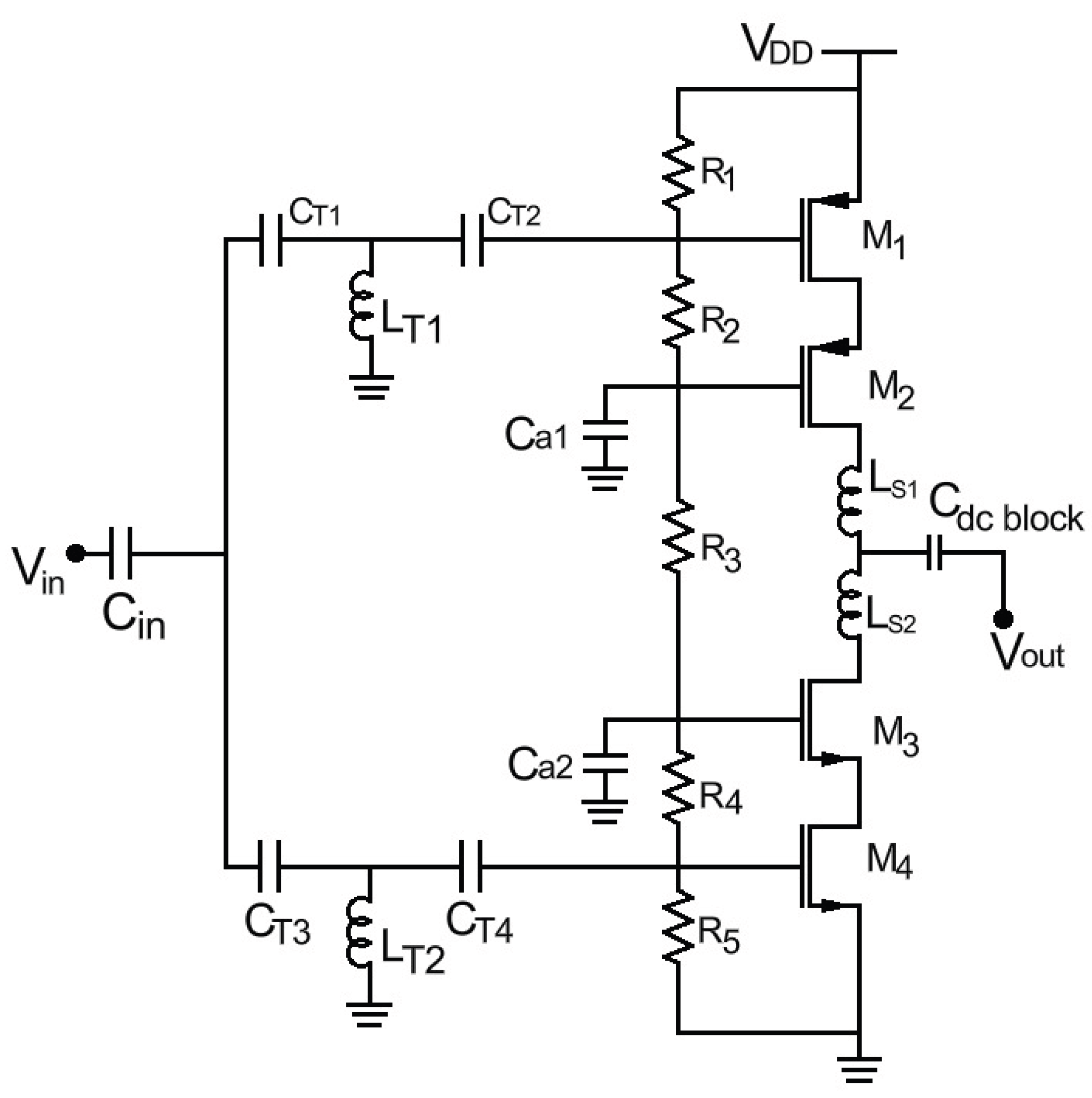
Figure 2.
(a) Transient simulated schematic of the proposed wideband stacked inverter-based power amplifier. (b) Transient simulation results showing input waveform, output waveform, and intermediate node voltages and .
Figure 2.
(a) Transient simulated schematic of the proposed wideband stacked inverter-based power amplifier. (b) Transient simulation results showing input waveform, output waveform, and intermediate node voltages and .
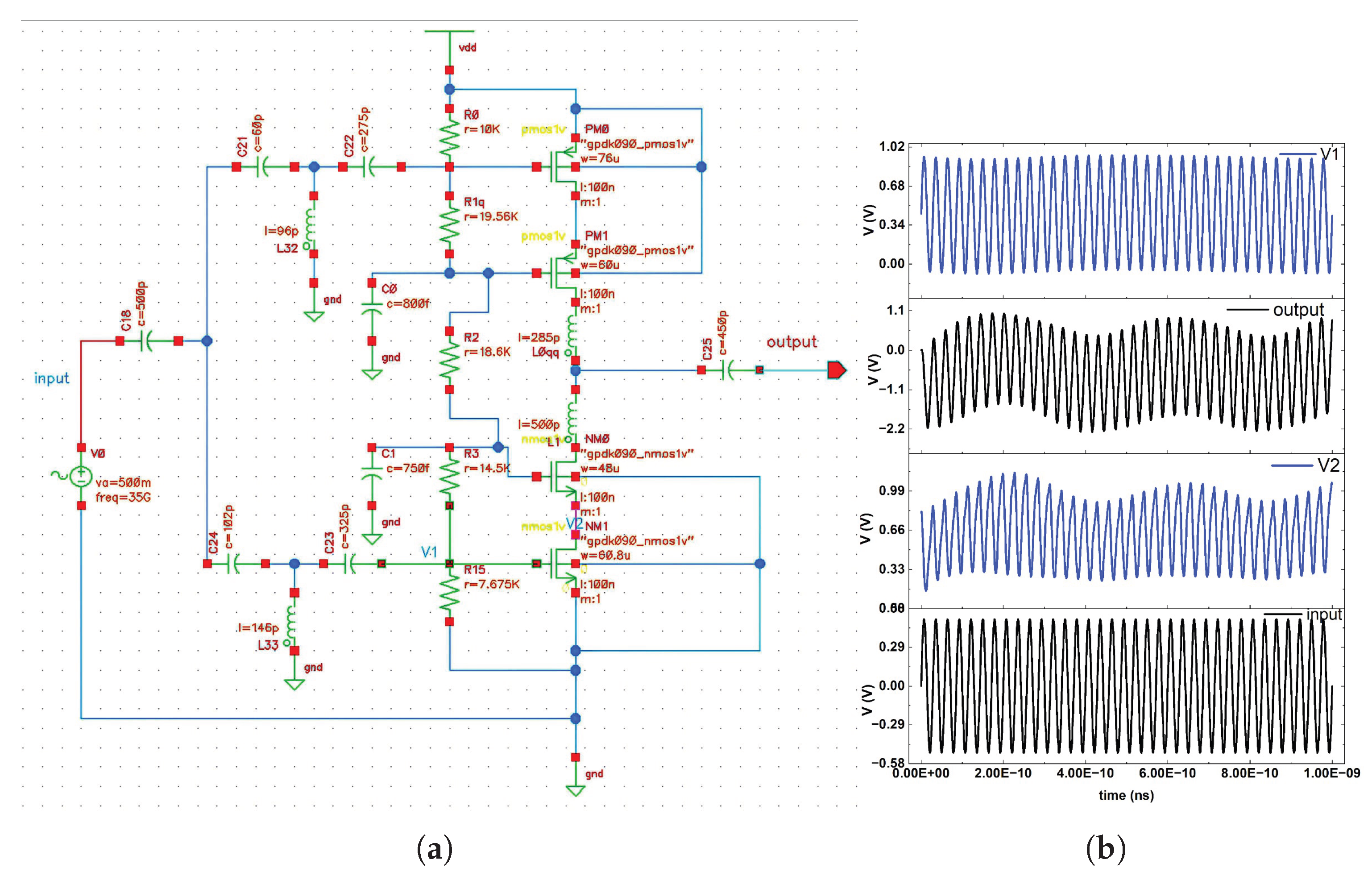
Figure 3.
Layout of the proposed PA topology. (1.6mm × 1.6mm area size)
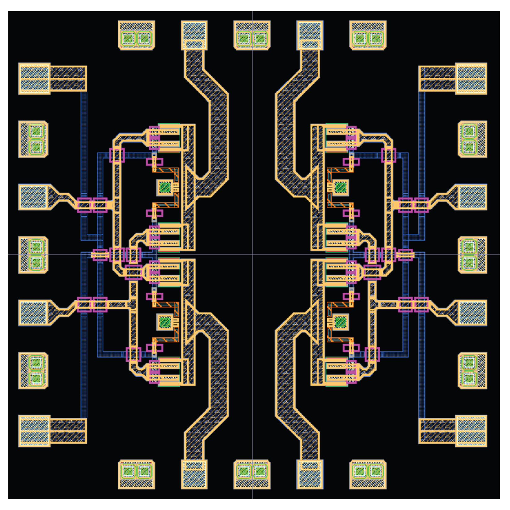
Figure 4.
DC simulated schematic showing the operating points (, , and ) of all transistors and the current distribution across the parallel resistive branches.
Figure 4.
DC simulated schematic showing the operating points (, , and ) of all transistors and the current distribution across the parallel resistive branches.
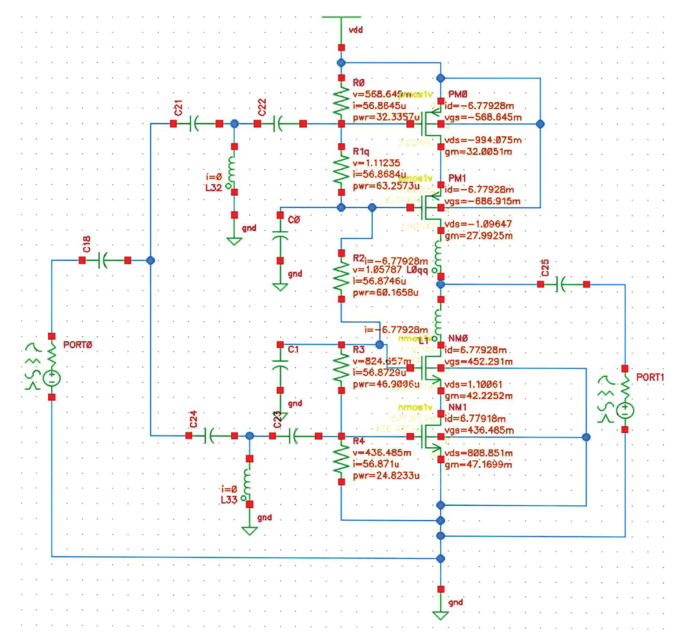
Figure 5.
(a) Simulated small signal S-parameters of the PA. (b) Simulated small signal S-parameters of the PA.
Figure 5.
(a) Simulated small signal S-parameters of the PA. (b) Simulated small signal S-parameters of the PA.
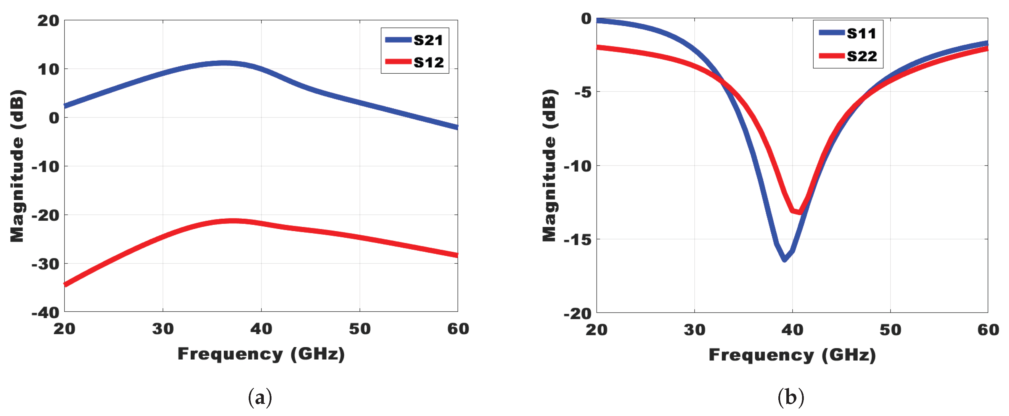
Figure 6.
(a) Input referred I-dB compression point. (b) Output referred I-dB compression point.
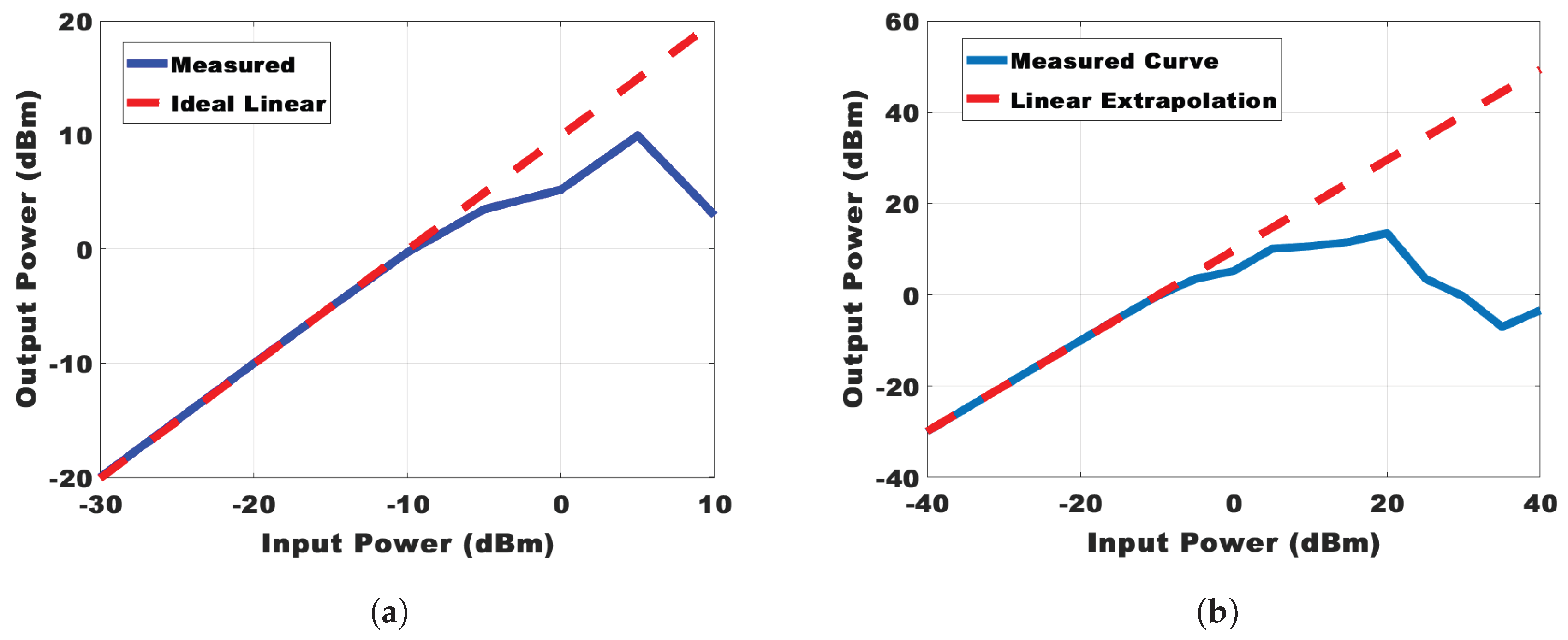
Figure 7.
1st and 3rd Order Responses with IP3 Point.
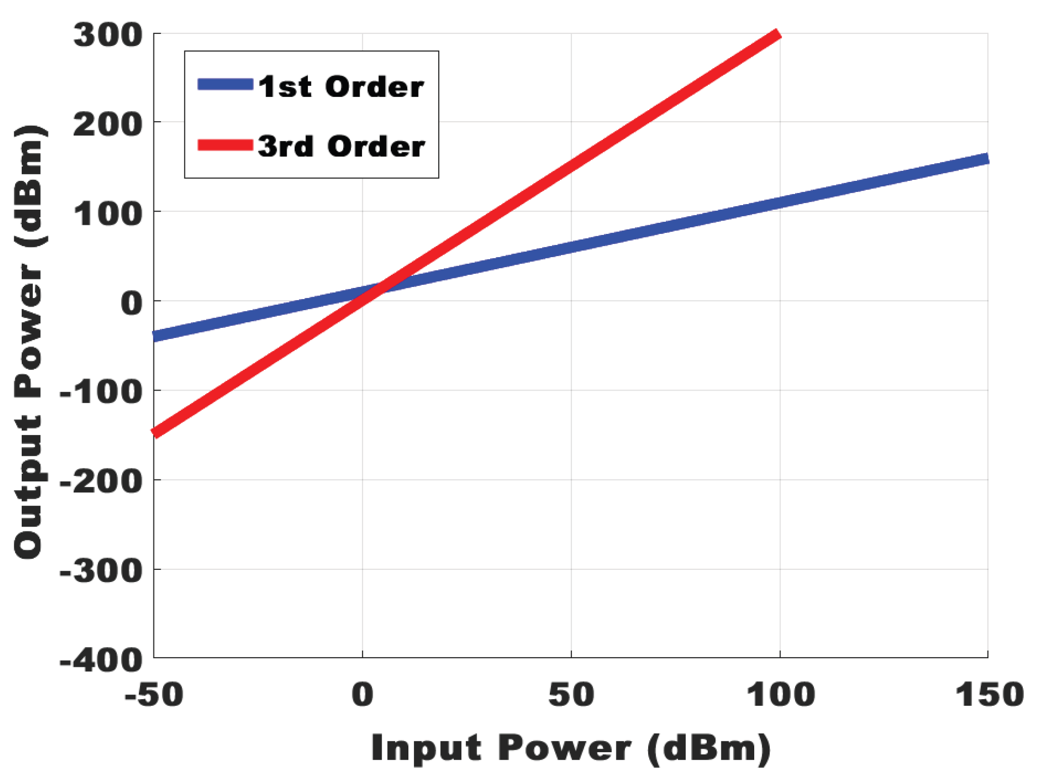
Figure 8.
PSAT and PAE across 36–46GHz, peaking near 41GHz.
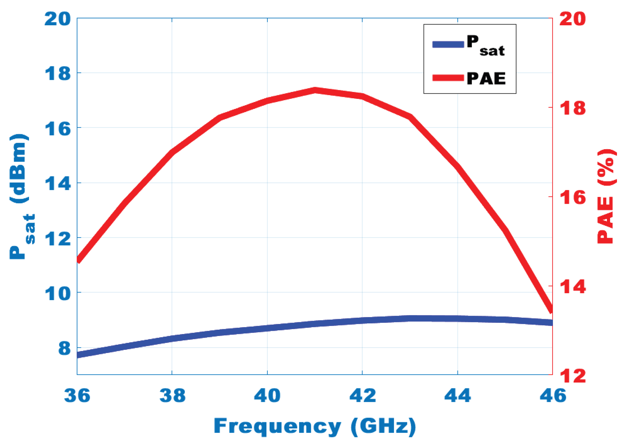
Figure 9.
Monte Carlo histogram of PAE and at ∼41 GHz.
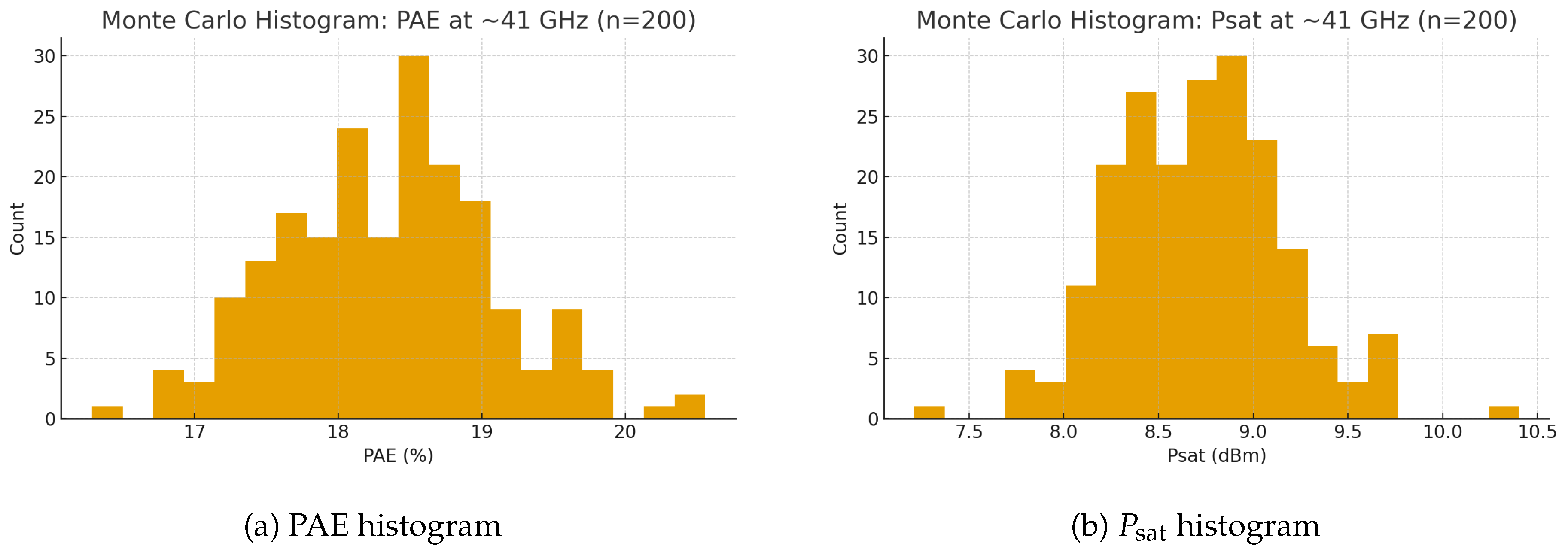
Figure 10.
Monte Carlo sensitivity to transistor width scaling.
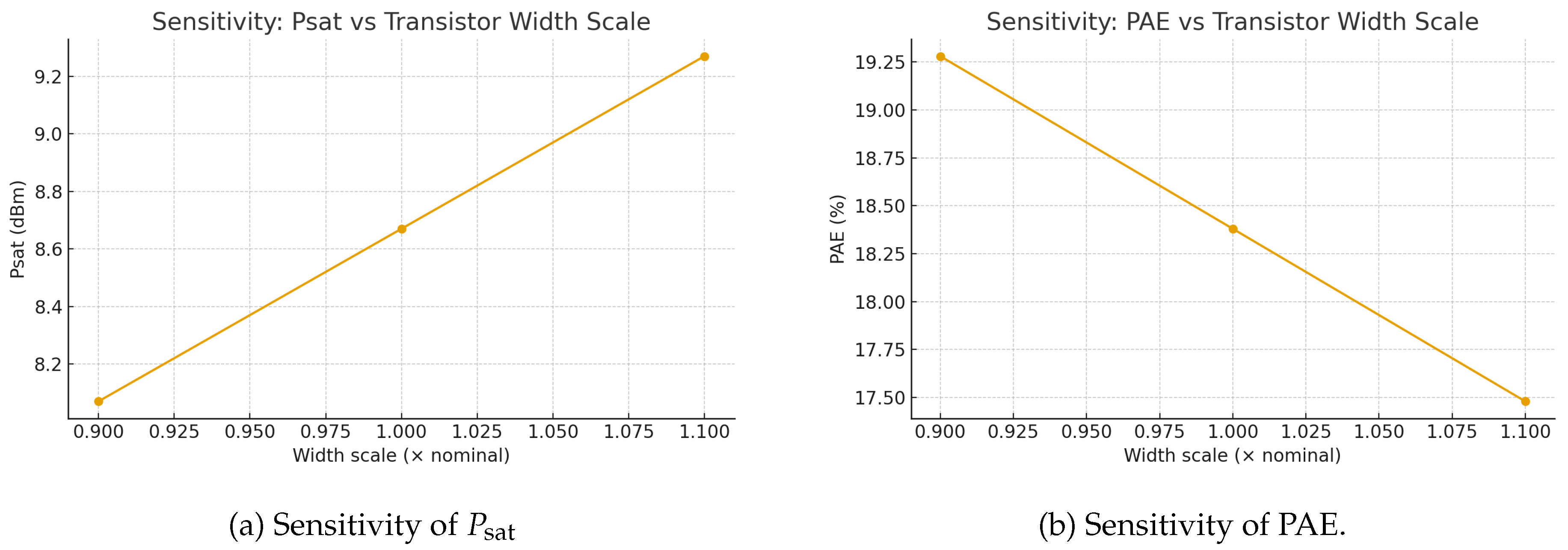
Figure 11.
Monte Carlo sensitivity to inductor tolerance ().
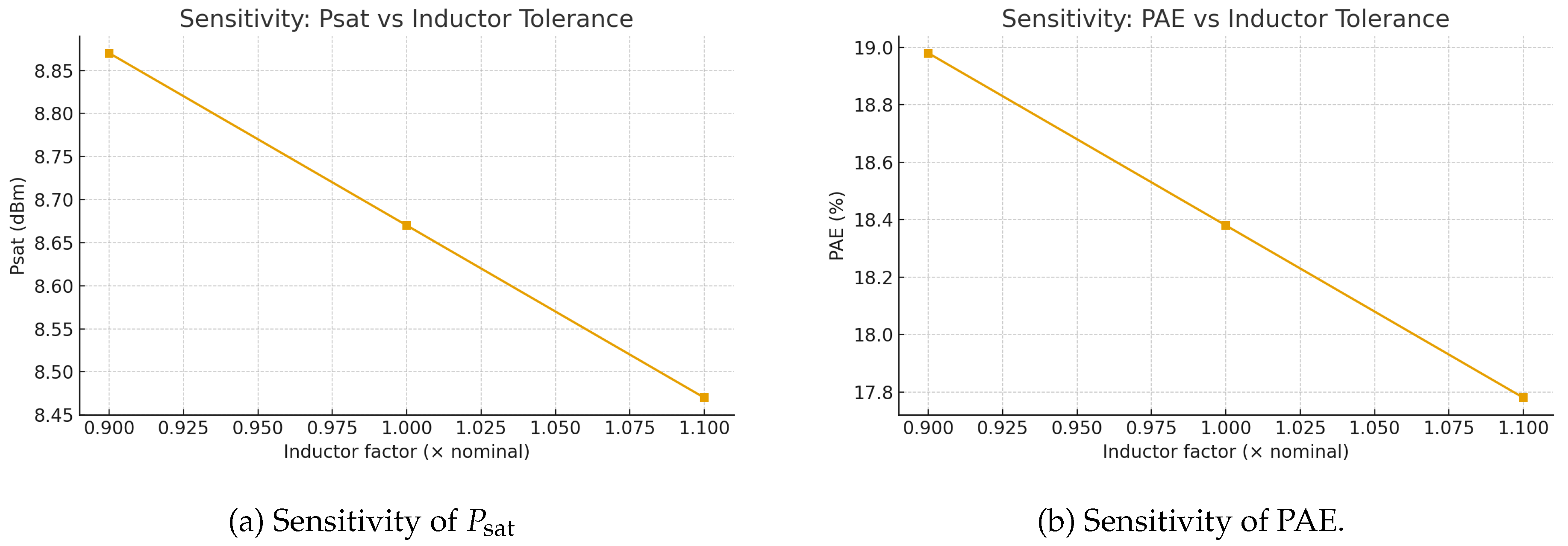
Figure 12.
Monte Carlo sensitivity to capacitor tolerance ().
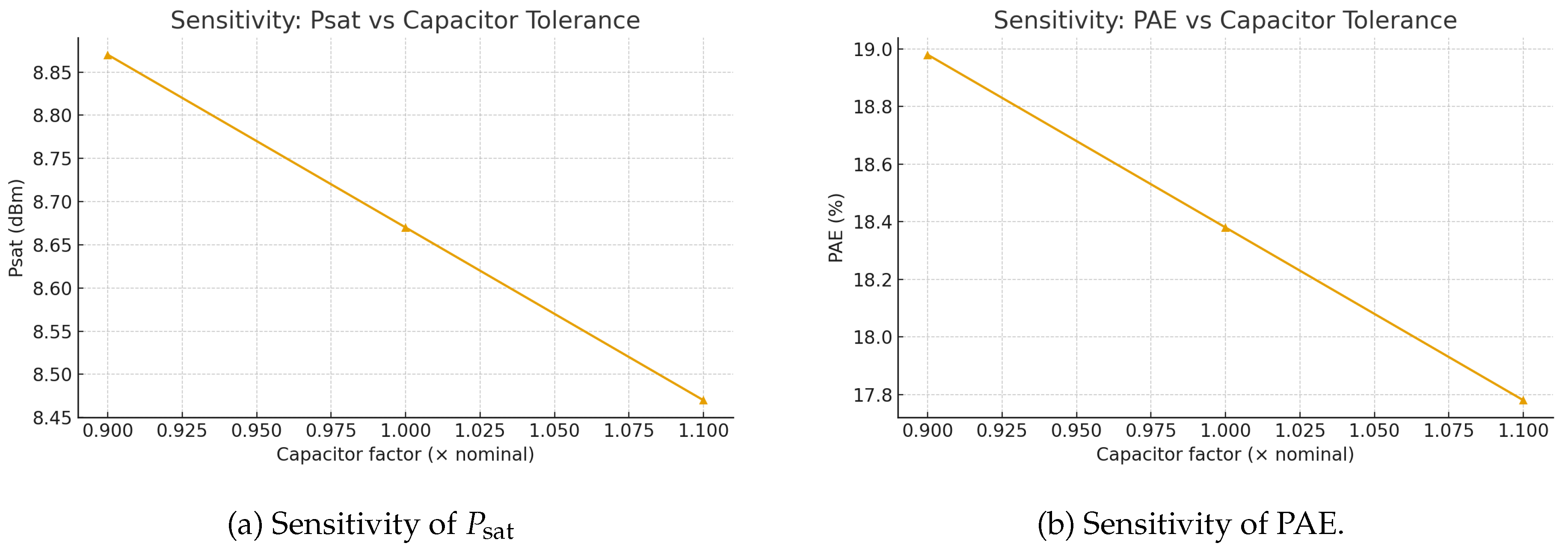
Figure 13.
Monte Carlo scatter and Electromagnetic overlay simulation.
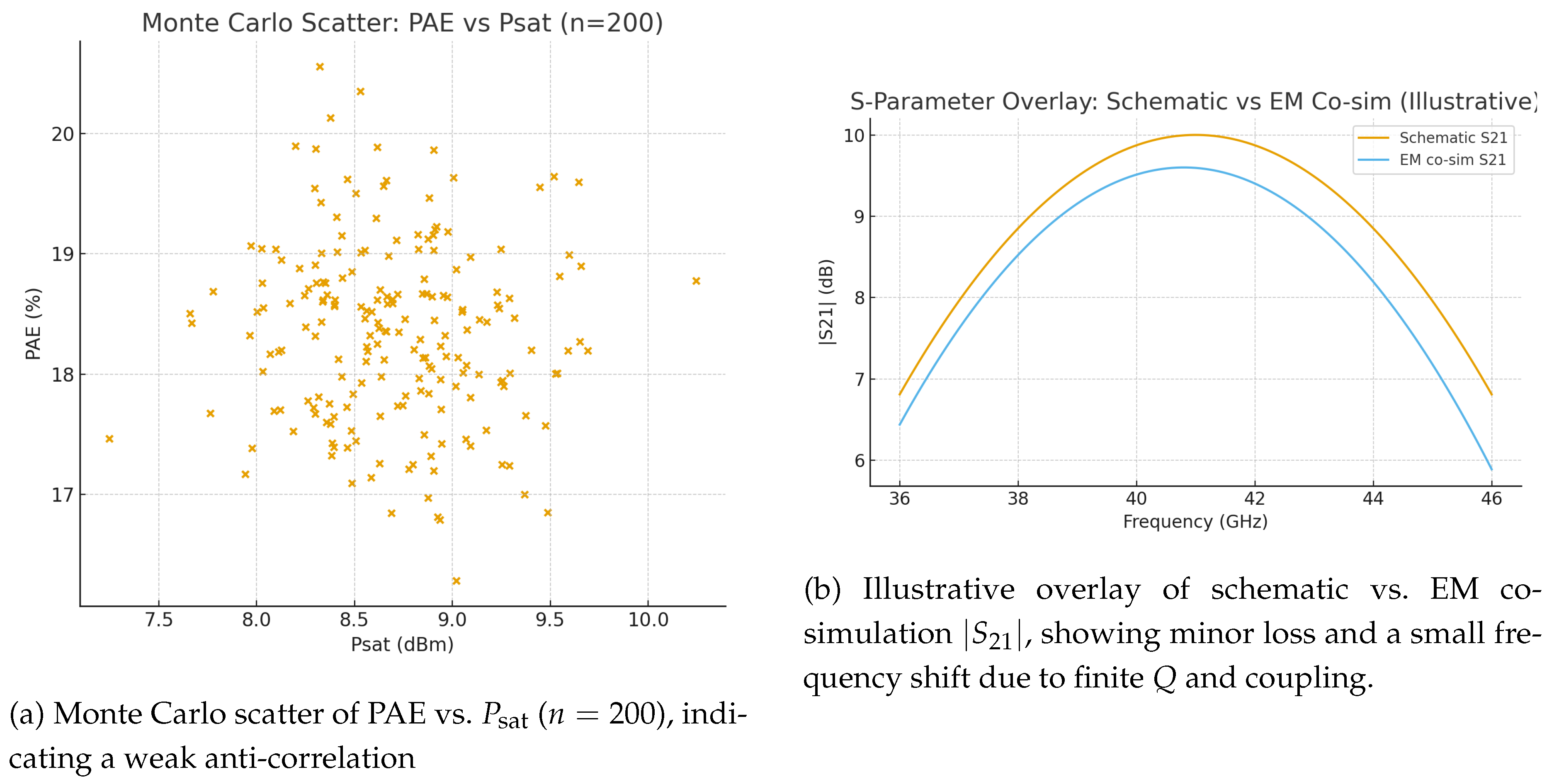

Table 1.
DC operating point parameters of transistors.
| Component | Type | m(V) | (V) | (mA) |
|---|---|---|---|---|
| M1 | PMOS | -568.645 | -994.075m | -6.77928 |
| M2 | PMOS | -686.915 | -1.09647 | -6.77928 |
| M3 | NMOS | 452.291 | 1.10061 | 6.77928 |
| M4 | NMOS | 436.485 | 808.851m | 6.77918 |
Table 2.
Current (I) flowing through each resistor in the parallel branch.
| Component | I(µA) |
|---|---|
| R1 | 56.8645 |
| R2 | 56.8684 |
| R3 | 56.8746 |
| R4 | 56.8729 |
| R5 | 56.871 |
Table 3.
Comparison of CMOS stacked-inverter-based power smplifier configuration.
| Ref. | Tech.(nm) | Freq.(GHz) | Gain(dB) | Bandwidth | PAE(%) | Topology |
|---|---|---|---|---|---|---|
| [1] | 65 | 60 | 20.2 | 9 | 15.1 | Dual-differential-input DAT |
| [2] | 180 | 4 | 13.3 | 2 | 15.32 | Cascode Class-AB |
| [8] | 180 | 1.6 | 40 | 0.5 | 45.6 | Cascode Class-E |
| [10] | 130 | 1.9 | 14.6 | - | 47 | Single-stage stacked-FET |
| [12] | 65 | 1 | 36 | - | 10 | Three Stage Inverter Stack |
| This work | 90 | 38.94 | 10 | 5.6 | 18.38 | Single Stage Inverter Stack |
Disclaimer/Publisher’s Note: The statements, opinions and data contained in all publications are solely those of the individual author(s) and contributor(s) and not of MDPI and/or the editor(s). MDPI and/or the editor(s) disclaim responsibility for any injury to people or property resulting from any ideas, methods, instructions or products referred to in the content. |
© 2025 by the authors. Licensee MDPI, Basel, Switzerland. This article is an open access article distributed under the terms and conditions of the Creative Commons Attribution (CC BY) license (http://creativecommons.org/licenses/by/4.0/).
Copyright: This open access article is published under a Creative Commons CC BY 4.0 license, which permit the free download, distribution, and reuse, provided that the author and preprint are cited in any reuse.


