
Submitted:
19 March 2025
Posted:
20 March 2025
You are already at the latest version
Abstract
The KSnI3 based perovskite solar cells have attracted a lot of research interest due their unique electronic, optical, and thermal properties. In this study, we optimized the performance of various lead-free perovskite solar cell structures—specifically, FTO/Al-ZnO/KSnI3/rGO/Se, FTO/LiTiO2/KSnI3/rGO/Se, FTO/ZnO/KSnI3/rGO/Se, and FTO/SnO2/KSnI3/rGO/Se, using the SCAPS-1D simulation tool. The optimization focused on the thicknesses and dopant densities of the rGO, KSnI3, Al-ZnO, LiTiO2, ZnO, and SnO2 layers, as well as the thickness of the FTO electrode. This, respectively, yielded the PCE values of 27.60%, 24.94%, 27.62%, and 30.44% for the FTO/Al-ZnO/KSnI3/rGO/Se, FTO/LiTiO2/KSnI3/rGO/Se, FTO/ZnO/KSnI3/rGO/Se, and FTO/SnO2/KSnI3/rGO/Se perovskite solar cell configurations. The FTO/SnO2/KSnI3/rGO/Se device is 7.66% more efficient than the FTO/SnO2/3C-SiC/KSnI3/NiO/C device, which is currently the highest performing KSnI3-based perovskite solar cell in the literature. Thus, our FTO/SnO2/KSnI3/rGO/Se perovskite solar cell structure is now, by far, the most efficient PSC design. Its best performance is achieved under ideal conditions of zero series resistance, shunt resistance of 107 Ω cm², and temperature of 371 K.
Keywords:
KSnI3
; rGO
; SnO2
; perovskite
; solar
1. Introduction
Perovskite solar cells (PSCs) are an emerging class of photovoltaic solar cells, in which materials known as perovskites are used as an active absorption layer. These materials have a unique crystal structure of the form ABX₃, where the A-site is occupied by larger cations, which can be organic molecules such as formamidinium or inorganic ions such as Cs [1]. The B-site is typically filled with a metal cation, such as lead or tin, while the X-site is filled with a halide ion such as iodine. This distinctive crystal arrangement gives perovskites their remarkable electronic and optical properties, such as high light absorption, fast charge-carrier mobility, and adjustable band gaps. Thus far, PSCs have shown outstanding improvement in their power conversion efficiency, with some laboratory prototypes even outperforming traditional silicon-based solar cells. Furthermore, their high efficiency presents a unique opportunity for large-scale and cost-effective manufacturing.
There is a wide range of PSCs based on different perovskite materials. Lead-based perovskite solar cells have been the most promising, achieving power conversion efficiency (PCE) of up to more than 25 % in a laboratory environment [2]. In fact, they are still an active area of research and have been showing improvement in various aspects in numerous computational and experimental studies (see Refs. [3,4,5,6,7,8,9,10,11] and references therein). For instance, the recent study of Ref. [3] investigated formamidinium lead iodide-based PSC using GPVDM software and obtained an improved PCE of 27.49%, which was also significantly higher than the PCE of the lead-free formamidinium tin iodide PSC that was also explored in the same study. Ref. [4] studied the CsPbX3-based perovskite solar cells using density functional theory (DFT) and SCAPS-1D (Solar Cell Capacitance Simulator) software and found CsPbIBr2 having the best balance between stability and band-gap, and yielding the maximum PCE of 16.53 %. In the same vein, Ref. [5] investigated HTM (hole transport material) free CsPbI3/CsSnI3 heterojunction solar cells, using the SCAPS-1D simulation tool, and achieved the PCE of up to 19.99%. Similarly, in the work of Ref. [6], the thickness optimization engineering of the electron transport, hole transport, and perovskite layers of MAPbI3-based PSC was performed using the SCAPS-1D simulation package. The study revealed the necessity to increase the layer thickness by 50 to 100%, and the improvement of the PCE by 1.5%, achieving the PCE of 22.10 %. Furthermore, in the study of Ref. [7], the CsPbI3, FAPbI3, MAPbI3, and FAMAPbI3 PSCs were analyzed and optimized using SCAPS-1D and results yielded the highest PCE of 26.35 % observed on the FAMAPbI3 -based perovskite solar cell. In the same interest, Ref. [8] conducted a numerical study on the CsPb.625Zn.375IBr2-based perovskite solar cells by optimizing the density of charge carriers, the density of defects, and thicknesses of the electron transport layer (ETL), hole transport layer (HTL), active absorption layer. This yielded a PCE of 21.05 % for the optimized structure. Furthermore, Ref. [9] performed a computational study of various perovskite solar cells, offering a detailed investigation of the impact of critical properties, such as band gap, electron affinity, layer thickness, absorption, recombination rate, band alignment, and defects, on the performance, and thus, achieving the highest PCE of 22.05% for the FAPbI3-based device. Ref. [10], investigated the effect of incorporating an interfacial layer of BiI3 in MAPbI3 and MAGeI3-based perovskite solar cells and improved the PCE from 19.28 to 20.30% for MAPbI3 PSC.
Even though lead-based PSCs are such a highly promising improvement in the photovoltaic industry, they have tremendous drawbacks. In particular, lead is a very toxic element that poses health risks to the manufacturers and consumers of lead-based perovskite solar cells. Thus, a lot of computational and experimental research is currently devoted to the development and optimization of lead-free perovskite solar cells [12,13,14,15,16,17,18,19,20,21,22]. One of such lead-free PSCs is the KSnI3-based device which is the subject of interest in the present study. This has recently attracted enormous interest, globally, due to its promising PCE, as well as the thermal and mechanical stability of KSnI3 perovskite material, making it ideal for usage as the active absorption layer in various PSC configurations [23]. In particular, Ref. [23] studied the structural, mechanical, and optical properties of KSnI3 using DFT, demonstrating its mechanical and thermal stability, and investigated its potential usage as the active absorption layer in perovskite solar cells using SCAPS-1D, and obtained the highest PCE of 9.776 % on the FTO/TiO2/KSnI3/Spiro-OMeTAD/W device. In the study of Ref. [24], the impact of organic charge transport layers was explored, and critical parameters such as dopant density, thickness, and defect density were optimized, yielding the highest PCE of 10.83 % for FTO/C60/KSnI3/PTAA/C structure. In the same vein, the theoretical study of Ref. [25] investigated the impact of metal phthalocyanines charge transport layers on KSnI3-based perovskite solar cells and obtained the optimized FTO/F16CuPc/KSnI3/CuPc/C architecture with PCE of 11.91 %. Another computational study was done by Ref. [26] using SCAPS-1D, exploring the effect of charge transport materials on the KSnI3-based PSC, and achieved the PCE of 9.28 % on the FTO/ZnOS/KSnI3/NiO/C configuration. Furthermore, the computational study of Ref. [27] made significant progress on the optimization of KSnI3 perovskite solar cells by achieving the PCE of 20.99 % for the FTO/ZnO/KSnI3/CuI/Au configuration, through the optimization of the hole transport layer, electron transport layer, anode material, defect and dopant densities. In the same interest, the very recent work Ref. [28] studied KSnI3 PSCs perovskite solar cells by optimization charge transport layers and incorporating the buffer layer, and obtained the highest PCE of 22.78 %, for the optimized FTO/SnO2/3C–SiC/KSnI3/NiO/C structure, which is currently the highest performance ever achieved on KSnI3-based PSCs. On the other hand, the recent computational optimization studies of Refs. [29,30,31] recently achieved the PCE of 31 % for CsSnI3-based PSCs, 27 % and 31.62 % for CsSnBr3-based PSCs when using rGO and WSe2 transport layers, which have never been investigated on KSnI3-based PSCs. Thus, there is still hope that the PCE of KSnI3-based PSCs can still be significantly improved using carefully chosen and optimized HTL and ETL materials.
In this work, we performed a computational optimization of FTO/Al-ZnO/KSnI3/rGO/Se, FTO/LiTiO2/KSnI3/rGO/Se, FTO/SnO2/KSnI3/rGO/Se, and FTO/ZnO/KSnI3/rGO/Se using the state-of-the-art SCAPS-1D simulation tool. Our choice of Al-ZnO, LiTiO2, ZnO, SnO2, and rGO was driven by their high charge mobility, strong thermal stability except for the case of ZnO, excellent conductivity, and optimal band alignment with KSnI3 [30,31,32,33,34,35]. Furthermore, rGO is known for having low trap states in the absorption layer/hole transport layer interface [36]. In particular, we optimized the aforementioned structures by varying the thickness of each layer, and the dopant density of ETLs, KSnI3, and rGO layers. This interestingly yielded tremendous improvement in the performance of KSnI3-based perovskite solar cells. This paper is structured as follows. Section 2 provides the details of the computational methods used in this study. Section 3 presents our results and their comparison with the literature, while section 4 contains the conclusions.
2. Computational Methods
2.1. Model Structure and Simulation Tools
The numerical modeling and optimization of perovskite solar cells can be achieved using various simulation tools, such as wxAMPS, PC-1D, AFORS-HET, TCAD, Silvaco, OghmaNano, and SCAPS-1D [37]. In the present study, we focused on the study of four perovskite solar cells using the SCAPS-1D simulation software. In particular, we optimized the performance of FTO/AlZnO/KSnI3/rGO/Se, FTO/LiTiO2/KSnI3/rGO/Se, FTO/ZnO/KSnI3/rGO/Se, and FTO/SnO2/KSnI3/rGO/Se PSC devices by tuning their dimensions and electronic properties within the SCAPS-1D numerical tool, which was chosen based on its reliability when compared to experimental data [38], and user-friendliness. The SCAPS-1D software package was developed at the University of Ghent by the Department of Electronics and Information Technology [37]. The structures of these PSC devices and the crystal structure of KSnI3 perovskite material are illustrated in Figure 1 and Figure 2, while the band alignment of ETLs and HTL with the perovskite layer is shown in Figure 3.
The simulations in the SCAPS-1D package are based on solving the following set of equations [30,37]:
In Poison´s equation (1), the quantities E, ψ, ε, ε0, n, p, NA, ND, pt, nt are, respectively, the electric field, electrostatic potential, relative permittivity, Permittivity of free space, the concentration of electrons, concentration of holes, density of ionized acceptor dopants, the density of ionized donor dopants, trapped hole and electron concentrations. In the transport equations (2) and (3), the parameters μn, μp, Dn, and Dp, are electron mobility, hole mobility, electron diffusion coefficient, and hole diffusion coefficient, respectively, while in the continuity equations (4) and (5), Gn, Gp, Un(n, p), and Up(n, p) are, respectively, electron generation rate, hole generation rate, electron recombination rate, and hole recombination rate. Poisson's equation describes the relationship between charge and electric field within a PSC, while the transport equations account for the migration of electrons and holes in the device, and the continuity equations trace the generation, recombination, and migration of electrons and holes in the PSC.
Table 1 presents the values of the properties of the KSnI3, ETL, HTL, and FTO used as input data in the SCAPS-1D simulation of the four perovskite solar cell devices. The parameters such as the thickness and dopant densities of different layers were later updated during the optimization process. Interface defect layers were also included using the data presented in Table 2.
In addition to the structural and electronic properties shown in tables 1 and 2, the simulation of perovskite solar cells requires the knowledge of the absorption coefficients of the active absorption layer material used in the simulations. In the SCAPS-1D simulation package, the absorption coefficients, Φ, are given by [29,30]
where the constants α and β are equal to 105 and 10-12, respectively, Eg is the active absorption layer band gap, while h and v are the Planck´s constant and frequency of incident photons, respectively.
2.2. Model and Material Validation
It is necessary to conduct SCAPS-1D model validation before the simulation of new perovskite solar cell structures. In this work we benchmarked our simulations by reproducing the FTO/SnO2/3C-SiC/KSnI3/NiO/C perovskite solar cell structure, which was optimized and proposed by Ref. [28] and is currently the most efficient KSnI3-based perovskite solar configuration in the literature. Table 3 shows the structural and electronic properties used in our benchmark simulation.
The corresponding performance metrics, which were obtained from this work, are presented in Table 4 where they are compared with the results of Ref. [28]. Our simulations yielded a PCE of 22.31 %, which is very close to the PCE of 22.78 % obtained by Ref. [28]. Thus, providing confidence in our SCAPS-1D model as well as the properties of FTO, SnO2, and KSnI3 that we incorporated in the SCAPS-1D software. Similarly, the accuracy of properties of AlZnO, LiTiO2, ZnO, and rGO, which were also used in this work, were verified in our previous work as discussed in Ref. [30]. Thus, we have confidence in our SCAPS-1D model and the properties of all materials used in this study.
3. Results
The optimization strategy followed in this study is two-fold. We started by optimizing the FTO/AlZnO/KSnI3/rGO/Se structure, by varying the thickness and dopant density of each layer in this structure. In this optimized structure we substituted AlZnO with other ETLs, namely LiTiO2, ZnO, and SnO2, of which we also optimized the thickness and donor dopant density to obtain optimized FTO/LiTiO2/KSnI3/rGO/Se, FTO/ZnO/KSnI3/rGO/Se, and FTO/SnO2/KSnI3/rGO/Se. The optimization of the aforementioned parameters was done as a result of the reasons discussed below.
The main function of the HTL in a perovskite solar cell is to effectively prevent the migration of electrons from the perovskite layer (PL) to the HTL, and allow the transmission of holes from the PL to the HTL and the anode [40]. However, if the thickness of the HTL is higher than the optimal thickness, the hole will have long paths to migrate within the HTL. As a result, the recombination probability will increase and the performance of the PSC will be poor. Similarly, if the HTL is thinner than its optimal thickness, the HTL will not be effective in extracting holes from the PL. Hence, the optimization of the HTL thickness is very crucial for improving the PCE of the perovskite solar cell. Similarly, the key function of the ETL is to extract electrons from the PL and transport them to the cathode. Its thickness also plays a vital role in the device's performance. For instance, it may yield low efficiency in charge collection if it is too thin, while it may decrease conductivity if it is too thick [41]. Furthermore, the major roles of a perovskite layer in a PSC are the attenuation of the solar spectrum within the visible-light energy range, and the generation of electron-hole pairs through the photovoltaic process. The thickness of the PL highly affects its performance. For instance, if the PL is too thick it will not have sufficient volume to absorb light and thus, yield a low density of excitons. On the other hand, if it is too thick, it reduces the performance of the PSC since the recombination rate increases with the increase in the PL thickness [31]. Therefore, it is very critical that the thickness of PL is optimized to achieve the highest possible performance of the PSC.
Similarly, the acceptor dopant density of the HTL, donor dopant density of the ETL, and acceptor dopant density of the active perovskite absorber layer play very crucial roles in the performance of perovskite solar cells. In particular, the separation of electron-hole pairs in PSC devices improves with the enhancement in the electric field that exists at the interface between the ETL and absorber layer, and at the interface between the HTL and absorber layer. The electric field strength increases with the increase in the donor dopant density of the ETL and acceptor dopant density of the HTL, and this improves the performance of the device [42]. Even the electric field within the PL depends on the dopant density of the PL, and this electric is also responsible for the reduction of recombinations within the PL [42]. However, if the dopant density is too high, it results in Coulomb traps which increase the likelihood of charge recombination. Thus, finding the optimal dopant densities of the ETL, HTL, and PL is very crucial for every PSC device.
3.1. Optimization of the Hole Transport Layer Thickness
In this work, we optimized the thickness of rGO HTL by varying it from 20 nm to 4000 nm and assessed its impact on the open circuit voltage (Voc), short-circuit current (Jsc), fill-factor (FF), and power conversion efficiency (PCE). The rest of the parameters were kept constant at their initial values shown in Table 1. The results are depicted in Figure 4. We observe that the Jsc increases fast as the rGO thickness increases towards 1000 nm, and thereafter remains relatively constant. On the other hand, Voc is relatively constant. In particular, Jsc ranges from 11.823 to 22.182 mA/cm2, while Voc ranges from 1.334 to 1.361 V. On the other hand, FF somewhat decreases as the rGO thickness approaches 500 nm, beyond which it is practically constant. The PCE shows a similar trend as Jsc. Quantitatively, FF ranges between 87.99 % and 87.39 %, while PCE is in the range of 13.88 to 26.38 %. The trends observed on the performance metrics are similar to the recent results of Refs. [42,43,44]. The increase in the Voc and PCE is attributed to the enhancement in hole extraction from the perovskite layer and transportation to the anode as the HTL thickness increases. The reduction in FF with the increase in HTL thickness may be due to the lateral resistance in the junction between HTL and the active absorption layer. The highest PCE is observed at 2670 nm. Thus, 2670 nm was deemed the optimal thickness of the rGO layer.
3.2. Optimization of the Hole Transport Layer Dopant Density
In this study, the acceptor dopant density of rGO was optimized by varying it between 2.5x1018 cm-3 and 1022 cm-3, and examined the dependence of Voc, Jsc, FF, and PCE on HTL acceptor dopant density, as shown in Figure 5. The thickness of this HTL was fixed at its optimal value of 2670 nm obtained in section 3.1, while the rest of the parameters were fixed at their values shown in table 1. The results show that Jsc and Voc do not change with the change in the acceptor dopant density of the rGO HTL. In contrast, FF and PCE somewhat increase as the acceptor dopant density rises towards 1020 cm-3 and 1019 cm-3, respectively, and thereafter remain constant. The notable increase in FF and PCE is due to the enhancement in the exciton separation as the result of the increase in electric field strength at the HTL/absorber interface [46]. In particular, Jsc is in the range of 22.17 to 22.26 mA/cm2, and Voc is 1.36 V. On the other hand, FF and PCE are in the ranges of 86.51 to 87.38 %, and 25.93 to 26.38 %, respectively. This highest PCE of 26.38 % is observed at the acceptor dopant density of 5.45x1021 cm-3. As a result, 5.45x1021 cm-3 was considered the optimal acceptor dopant density of rGO.
3.3. Optimization of Perovskite Layer Thickness
In the present study, we optimized the thickness of the KSnI3 active absorption layer by varying it from 50 nm to 1000 nm, and kept the thickness and acceptor dopant density of the HTL at their optimal values obtained in sections 3.1 and 3.2, while the rest of the parameters were kept at their respective values provided in Table 1. The variation of Voc, Jsc, FF, and PCE with PL thickness is depicted in Figure 6. We observe that Jsc and Voc do not significantly change as the KSnI3 layer thickness increases. On the other hand, the FF, and PCE are decreasing functions of PL thickness in the entire 50 nm to 1000 nm region. In particular, Jsc, Voc, FF, and PCE range from 22.02 mA/cm2 to 22.18 mA/cm2, 1.34 V to 1.36 V, 87.65 % to 83.75 %, and 26.50% to 24.76%, respectively. Clearly, the performance of the PL deteriorates with the increase in its thickness. This is due to the increase in recombination rate with the increase in the perovskite layer thickness [31,47]. Thus, the optimal thickness of the PL was considered to be 50 nm, at which the highest PCE is observed.
3.4. Optimization of Perovskite Layer Acceptor Dopant Density
We optimized the acceptor dopant density of the perovskite layer by varying it from 1019 cm-3 to 1022 cm-3 and examined the dependence of the Voc, Jsc, FF, and PCE on the dopant density. During this process, the thickness and dopant density of the HTL were at their optimal values obtained in sections 3.1 and 3.2, the thickness of the PL was fixed at its optimal value obtained in section 3.3, and the rest of the parameters were kept at their respective values provided in table 1. Figure 7 presents Voc, Jsc, FF, and PCE as a function of the acceptor dopant density of the PL. It was observed that Jsc decreases with the increase in dopant density, and it ranges between 14.40 mA/cm2 and 22.16 mA/cm2. In contrast, Voc increases slowly with the increase in the PL acceptor dopant density. In particular, it ranges from 1.36 V to 1.48 V. This rise in Voc is the reflection of the increase in built-in potential, resulting from the increase in the acceptor dopant density [48]. Similarly, the FF rises as the dopant density increases towards 1021 cm-3, and thereafter, remains relatively constant. In particular, it is in the range of 84.10 % and 91.10 %. This increase in the FF corresponds to the reduction in the resistivity of the absorption layer [49]. On the other hand, the PCE slightly rises as the dopant density approaches 1021 cm-3, above which it is a decreasing function of the acceptor dopant density. Quantitatively, PCE has the lowest value of 19.45% and the highest value of 27.36 %. The notable reduction in Jsc and PCE with the increase in dopant density may be attributed to the decrease in charge carrier mobility and rise in charge recombination rate [17,50,51]. The highest PCE occurs at the dopant density of 8.33x1020 cm-3, which is therefore considered the optimal acceptor dopant density of the PL.
3.5. Optimization of Electron Transport Layer Thickness
In the present study, the thickness of the Al-ZnO electron transport layer was optimized through its variation from 50 nm to 4000 nm. The other parameters were fixed at their optimal values found in sections 3.1 to 3.4, while those that have not been optimized were kept at their initial values shown in table 1. The dependence of Voc, Jsc, FF, and PCE on the Al-ZnO thickness is presented in Figure 8. The Jsc and PCE are relatively constant at thicknesses smaller than 1000 nm, and then slowly decline as the thickness increases. In particular, Jsc is in the range of 20.56 to 21.16 mA/cm2, while PCE ranges between 26.58 % and 27.37 %. The Voc and FF on the other hand remain practically stable, at 1.43 V and 90.52 %, in the entire 50 nm to 4000 nm ETL thickness range. Thus, it is clear that the overall performance of the PSC device slightly declines as the Al-ZnO becomes thicker. This observation is consistent with the literature. It could be attributed to the increase in resistance and deterioration in conductivity as a result of the increase in ETL thickness [30,47]. The highest PCE is observed at the Al-ZnO thickness of 489 nm, which was, thus, considered the optimal thickness of the Al-ZnO ETL.
3.6. Optimization of Electron Transport Layer Donor Dopant Density
In this work, we found the optimal donor dopant density of the Al-ZnO electron transport layer by examining how it affects Voc, Jsc, FF, and PCE. These performance metrics were assessed in the 1015 to 1020 cm-3 donor dopant density range, as depicted in Figure 9. The results reveal that Jsc and Voc are unaffected by the change in donor dopant density of Al-ZnO, and they are in the range of 21.16 to 21.17 mA/cm2 and 1.41 to 1.43 V, respectively. The FF and PCE are relatively constant donor dopant densities smaller than 1018 cm-3, and thereafter slowly decrease with the increase in the donor dopant density. In particular, they are in the range of 89.69 to 90.81%, and 27.50 to 26.86 %, respectively. Thus, the overall performance of the device slightly deteriorates with the increase in the donor dopant density of the Al-ZnO layer, at high dopant densities. This may be due to Coulomb traps which are understood to result from high dopant concentrations and cause a reduction in charge mobility [52,53]. The highest value of PCE occurs at the dopant density of 1015 cm-3, which was therefore deemed the optimal donor dopant density of the Al-ZnO ETL.
3.7. Optimization of FTO Layer Thickness
We also optimized the thickness of the FTO layer by varying it between 100 nm and 4000 nm, and assessed the impact of this on the Voc, Jsc, FF, and PCE, as presented in Figure 10. The results show the performance metrics do not change much as the thickness increases. The Jsc varies between 20.91 mA/cm2 and 21.28 mA/cm2, and Voc remains 1.43 V. FF ranges from 90.60 to 90.68 %, and PCE ranges from 27.15 to 27.60 %. Thus, the device performance is not highly affected by the FTO thickness. The slight decline in Jsc and PCE at low FTO thickness may be attributed to the increase in series resistance and optical losses which are correlated to the increase in the FTO thickness. The highest PCE occurs at the thickness of 100 nm, which was, therefore, deemed the optimal thickness of the FTO layer.
This is the end of the optimization of the FTO/Al-ZnO/KSnI3/rGO/Se structure. It was used as the framework for optimization of the FTO/LiTiO2/KSnI3/rGO/Se, FTO/ZnO/KSnI3/rGO/Se, and FTO/SnO2/KSnI3/rGO/Se configurations, as presented in the next sections.
3.8. Substitution of Al-ZnO Electron Transport Layer
In the further analysis, we found the optimal FTO/LiTiO2/KSnI3/rGO/Se, FTO/ZnO/KSnI3/rGO/Se, and FTO/SnO2/KSnI3/rGO/Se PSC configurations by substituting Al-ZnO with LiTiO2, ZnO, and SnO2 in the optimized FTO/Al-ZnO/KSnI3/rGO/Se structure. During this process, the thicknesses and dopant densities of rGO, KSnI3, and FTO layers were kept at their optimal values found in the previous sections, while the thicknesses and donor dopant densities of LiTiO2, ZnO, and SnO2 were varied to assess their impact on Voc, Jsc, FF, and PCE.
3.8.1. Optimization of LiTiO2, ZnO and SnO2 Thickness
The ETL thicknesses of the FTO/LiTiO2/KSnI3/rGO/Se, FTO/ZnO/KSnI3/rGO/Se, and FTO/SnO2/KSnI3/rGO/Se perovskite solar cell structures were optimized by varying the thicknesses of LiTiO2, ZnO, and SnO2 from 100 nm to 4000 nm, and observed the dependence of Voc, Jsc, FF, and PCE on the thickness. The results are depicted in Figure 11. We observe that for ETL = LiTiO2, ZnO, and SnO2, Voc is relatively constant in the entire 100 to 4000 nm ETL thickness range. In particular, Voc is 1.30 V, 1.43 V, and 1.53 V for LiTiO2, ZnO, and SnO2, respectively. The Jsc corresponding to SnO2 and ZnO is relatively stable in the whole thicknesses range, while for LiTiO2 it slightly decreases as the thickness approaches 1500 nm and thereafter remains constant. In particular, Jsc is in the range of 20.13 to 21.25 mA/cm2, 20.93 to 21.26 mA/cm2, and 21.16 to 21.25 mA/cm2 for LiTiO2, ZnO, and SnO2, respectively.
The results also show that FF is practically constant for all ETL materials. Quantitatively, it is in the range of 91.25 to 91.27 % for SnO2, 90.04 to 90.81 % for ZnO, and 89.72 to 89.95 % for LiTiO2. Furthermore, PCE shows trends similar to Jsc. It is relatively stable for ZnO, and SnO2, while for LiTiO2 it somewhat decreases as the thickness rises towards 1000 nm and thereafter remains unaffected by the thickness. In particular, it ranges from 23.57 to 24.91 % for LiTiO2, 27.03 to 27.64 % for ZnO, and 29.53 to 29.67 % for SnO2. Thus, the thickness of ZnO, and SnO2 does not have a significant impact on the overall performance of FTO/ZnO/KSnI3/rGO/Se, and FTO/SnO2/KSnI3/rGO/Se devices, while the increase in the thickness of LiTiO2 slightly reduces the overall performance of the FTO/LiTiO2/KSnI3/rGO/Se device. The deterioration in the PCE and Jsc, for LiTiO, with the increase in the ETL thickness may result from an increase in series resistance, and the low transmission of light through the ETL layer [49]. The highest PCE is observed at 50 nm for LiTiO2 and ZnO, and 489 nm for SnO2. Thus, these were considered the optimal thicknesses of LiTiO2, ZnO, and SnO2, in the FTO/LiTiO2/KSnI3/rGO/Se, FTO/ZnO/KSnI3/rGO/Se, and FTO/SnO2/KSnI3/rGO/Se PSC structures.
3.8.2. Optimization of LiTiO2, ZnO and SnO2 Donor Dopant Density
The donor dopant density of the LiTiO2, ZnO, and SnO2 electron transport layers was optimized, by varying it between 1012 and 1019 cm-3, and observing its effect on the Jsc, Voc, FF, and PCE, while keeping the rest of the parameters at their optimal values found in the previous sections. As depicted in Figure 12, the results show that Jsc, Voc, FF, and PCE are not significantly affected by the donor dopant density of LiTiO2, ZnO, and SnO2. Thus, the donor dopant densities of LiTiO2, ZnO, and SnO2 do not have a significant impact on the overall performance of the FTO/LiTiO2/KSnI3/rGO/Se, FTO/ZnO/KSnI3/rGO/Se, and FTO/SnO2/KSnI3/rGO/Se solar cells. These observations are consistent with the recent literature [43]. In particular, Jsc is in the range of 21.25 to 21.26 mA/cm2 for LiTiO2, 21.25 to 21.26 mA/cm2 for SnO2, and 21.26 to 21.27 mA/cm2 for ZnO. Voc is 1.30 V for LiTiO2, 1.53 V for SnO2, and 1.43 V for ZnO. Furthermore, FF is 89.63 to 90.01 % for LiTiO2, 91.01 to 91.28% for SnO2, and 90.52 to 90.79 % for ZnO. The PCE, on the other hand, is in the range of 24.77 to 24.94 % for LiTiO2, 29.67 to 29.53 % for SnO2, 27.51 to 27.62 % for ZnO. The highest PCEs are observed at the donor dopant densities of 1012 cm-3 for LiTiO2, and 1016 cm-3 for SnO2 and ZnO. Thus, these were deemed the optimal donor dopant densities for ETL = LiTiO2, ZnO, and SnO2.
3.9. Optimized Parameters and Performance Metrics
Table 5 presents the optimized parameters of FTO/Al-ZnO/KSnI3/rGO/Se, FTO/LiTiO2/KSnI3/rGO/Se, FTO/ZnO/KSnI3/rGO/Se, and FTO/SnO2/KSnI3/rGO/Se PSC structures. The rest of the parameters remained unchanged as shown in Tables 1.
Table 6 presents the performance metrics of the optimized PSC structures. These correspond to the optimized structural and electronic properties shown in table 3. It is clear that FTO/SnO2/KSnI3/rGO/Se has the highest PCE. Thus, it became our main focus in the rest of the analysis.
3.10. Effect of Series and Shunt Resistance
Series resistance (Rs) and shunt resistance (Rsh) are some of the crucial parameters that highly affect the performance of perovskite solar cells. Failure to optimize them may result in poor performance of the PSC device. Series resistance is understood to exist at various contact points of the device such as anode, cathode, and interfaces. On the other hand, shunt resistance is a desired property in a PSC and it prevents the flow of undesired shunt current which reduces the net current of the device. In this study, we investigated the effect of the Rs and Rsh on the performance of our highest-performing PSC structure which is FTO/SnO2/KSnI3/rGO/Se. In particular, we varied Rs and Rsh from 0 to 8 Ω cm2, and 0 to 108 Ω cm2, respectively, while other parameters were kept at the optimal values found in the previous sections. The results are presented in Figure 13 and Figure 14. We observe that Jsc and Voc are unaffected by the change in Rs, while FF and PCE are both decreasing functions of Rs. In particular, Jsc and Voc are 21.25 mA/cm2 and 1.53 V, respectively, while FF and PCE are in the range of 91.27 to 80.51 % and 29.67 to 26.19 %, respectively. Thus, the overall performance of the FTO/SnO2/KSnI3/rGO/Se device deteriorates with the increase in Rs. These results are similar to other observations in the literature Ref. [31]. The decline in the FF with an increase in Rs is consistent with the dependence of FF on Rs, given by FF = FF0(1 – Rs) where FF0 is the fill factor in the absence of series resistance [29].
Furthermore, the change in Rsh also does not affect the Jsc, while Voc, FF, and PCE rapidly rise as the Rsh approaches 107 Ω cm2 above which they remain relatively stable. This is consistent with the observations of Ref. [29]. Quantitatively, Jsc is 21.25 mA/cm2 in the whole Rsh region, while Voc, FF, and PCE are in the range of 0.213 to 1.53 V, 18.74 to 91.27 %, 0.8463 to 29.67 %, respectively. Thus, 107 Ω cm2 was deemed the optimal Rsh for the FTO/SnO2/KSnI3/rGO/Se PSC device.
3.11. Effect of Temperature
Temperature is also a critical factor that can highly influence the overall performance of the perovskite solar device. In this study, we examined the effect of the temperature on Jsc, Voc, FF, and PCE of the FTO/SnO2/KSnI3/rGO/Se configuration by varying the temperature from 300 K to 400 K. The rest of the parameters were fixed at their optimal values found above. The results are shown in Figure 15, and reveal that Voc remains constant, while Jsc slowly rises with the increase in temperature. The gradual increase in Jsc corresponds to the reduction in the band gap of the absorption layer, resulting in the enhancement in the generation of electron-hole pairs [54,55]. The PCE follows the same increasing trend as Jsc. This is similar to the recent observations of Ref. [56]. On the other hand, FF decreases with the increase in temperature. This is consistent with the temperature dependence of FF given by [6].
where nkT/q is the thermal voltage. Quantitatively, Jsc, Voc, FF, and PCE range from 21.25 to 22.15 mA/cm2, 1.53 to 1.54 V, 91.27 to 89.20 %, 29.67 to 30.44 %, respectively. The highest PCE is observed at 371 K and this was considered the optimal operation temperature for the FTO/SnO2/KSnI3/rGO/Se PSC structure.
Table 7 presents the performance metrics of the optimized PSC structures when the optimal Rs, Rsh, and temperature of 0, 107 Ω cm2, and 371 K, respectively, are assumed. These also correspond to the optimized structural and electronic properties shown in table 5.
3.12. Comparison of Results with Literature
Table 8 shows the Voc, Jsc, FF, and PCE of the optimized FTO/Al-ZnO/KSnI3/rGO/Se, FTO/LiTiO2/KSnI3/rGO/Se, FTO/ZnO/KSnI3/rGO/Se, and FTO/SnO2/KSnI3/rGO/Se PSC structures, and Voc, Jsc, FF, and PCE of all KSnI3 perovskite solar cells available in the literature. All our investigated PSC configurations are higher than the PCE of 22.78 % which is currently the highest PCE of KSnI3-based perovskite solar cells. In fact, the highest performing PSC structure, FTO/SnO2/KSnI3/rGO/Se, has a PCE of 30.44 % under ideal Rs, Rsh and temperature conditions. This is 7.66 % more efficient than the FTO/SnO2/3C–SiC/KSnI3/NiO/C which is the highest-performing PSC known in the literature thus far.
4. Conclusions
In this study, we optimized FTO/Al-ZnO/KSnI3/rGO/Se, FTO/LiTiO2/KSnI3/rGO/Se, FTO/ZnO/KSnI3/rGO/Se, and FTO/SnO2/KSnI3/rGO/Se PSC structures using the SCAPS-1D simulation package. In particular, we optimized the thicknesses and dopant densities of rGO, KSnI3, Al-ZnO, LiTiO2, ZnO, and SnO2 layers, as well as the thickness of FTO. This yielded the PCE of 27.60 %, 24.94 %, 27.62 %, and 30.44 % for FTO/Al-ZnO/KSnI3/rGO/Se, FTO/LiTiO2/KSnI3/rGO/Se, FTO/ZnO/KSnI3/rGO/Se, and FTO/SnO2/KSnI3/rGO/Se, respectively. Thus, the PCE of FTO/SnO2/KSnI3/rGO/Se is 7.66 % higher than the PCE of FTO/SnO2/3C–SiC/KSnI3/NiO/C, which is currently the highest performing KSnI3-based perovskite solar cells in the literature. Thus, we propose FTO/SnO2/KSnI3/rGO/Se as the new highest-performing KSnI3-based PSC. We also call for experimental studies to further verify and improve the proposed configuration. The ideal performance conditions of this newly developed PSC configuration are series resistance of zero, shunt resistance of 107 Ω cm2, and temperature of 371 K. The series resistance of zero is impossible to achieve in real life, but this work shows that it should be minimized as much as possible.
Author Contributions
All authors contributed significantly to the manuscript.
Data Availability Statement
All data presented in this article are available on request.
Conflicts of Interest
The authors declare that there is no conflict of interest in this work.
Ethical approval
This research work does not involve humans or animals.
References
- R. A. Afre and D. Pugliese, “Perovskite Solar Cells: A Review of the Latest Advances in Materials, Fabrication Techniques, and Stability Enhancement Strategies,” Micromachines, vol 15, pp. 192, 2024. [CrossRef]
- H. Min et al., “Perovskite solar cells with atomically coherent interlayers on SnO2 electrodes.” Nature, vol 598, pp. 444–450, 2021. [CrossRef]
- R. Rani, K. Monga, S., Chaudhary, “Simulation of efficient Sn/Pb-based formamidinium perovskite solar cells with variation of electron transport layers,” Phys. Scr., vol 98, pp. 075910, 2023. [CrossRef]
- D. Saikia et al., “Numerical simulation of all inorganic CsPbIBr2 perovskite solar cells with diverse charge transport layers using DFT and SCAPS-1D frameworks,” Phys Scr., vol 99, pp. 095946, 2024. [CrossRef]
- X. Xu et al., “Design of all-inorganic hole-transport-material-free CsPbI3/CsSnI3 heterojunction solar cells by device simulation,” Mater. Res. Express, vol 9, pp. 025509, 2022. [CrossRef]
- M. Aliaghayee, “Optimization of the Perovskite Solar Cell Design with Layer Thickness Engineering for Improving the Photovoltaic Response Using SCAPS-1D,” J. Electron. Mater., vol 52, pp. 2475, 2023. [CrossRef]
- P. Subudhi and D. Punetha, “Pivotal avenue for hybrid electron transport layer-based perovskite solar cells with improved efficiency,” Sci. Rep., vol 13, pp. 19485, 2023. [CrossRef]
- M. Hossain et al., “Design and simulation of CsPb.625Zn.375IBr2-based perovskite solar cells with different charge transport layers for efficiency enhancement,” Sci. Rep., vol 14, pp. 30142, 2024. [CrossRef]
- S. T. Jan and M. Noman, “Comprehensive analysis of heterojunction compatibility of various perovskite solar cells with promising charge transport materials,” Sci. Rep., vol 13, pp. 19015, 2023. [CrossRef]
- M. Noman, A. H. H. Khan, and S. T. Jan, “Interface engineering and defect passivation for enhanced hole extraction, ion migration, and optimal charge dynamics in both lead-based and lead-free perovskite solar cells,” Sci. Rep., vol 14, pp. 5449, 2024. [CrossRef]
- X. Shaobing et al., “Reducing nonradiative recombination for highly efficient inverted perovskite solar cells via a synergistic bimolecular interface,” Nat. Commun., vol 15, pp. 5607, 2024. [CrossRef]
- L. Huang and W. R. L. Lambrecht, “Electronic band structure, phonons, and exciton binding energies of halide perovskites CsSnCl3, CsSnBr3 and CsSnI3,” Phys. Rev. B, vol 88, pp. 165203, 2013. [CrossRef]
- R. Rani, K. Monga, K. and S. Chaudhary, “Simulation of efficient Sn/Pb-based formamidinium perovskite solar cells with variation of electron transport layers,” Phys. Scr., vol 98, pp. 075910, 2023. [CrossRef]
- S. Lin et al., “Inorganic Lead-Free B-γ-CsSnI3 Perovskite Solar Cells Using Diverse Electron-Transporting Materials: A Simulation Study,” ACS Omeg, vol 6, pp. 26689−26698, 2021. http://pubs.acs.org/journal/acsodf.
- P. K. Patel, “Device simulation of highly efficient eco-friendly CH3NH3SnI3 perovskite solar cell,” Sci. Rep., vol 11, pp. 3082, 2021. [CrossRef]
- M. K. Hossain et al., “An extensive study on multiple ETL and HTL layers to design and simulation of high-performance lead-free CsSnCl3-based perovskite solar cells,” Sci. Rep., vol 13, pp. 2521, 2023. [CrossRef]
- M. Wang et al., “Lead-free perovskite materials for solar cells,” Nano-Micro Lett., vol 13, pp. 62, 2023. [CrossRef]
- Y. Liang et al., “Electrode-induced impurities in tin halide perovskite solar cell material CsSnBr3 from first principles,” Npj Comp. Mater., vol 7, pp. 63, 2021. [CrossRef]
- M. Jiang, “Simulated development and optimized performance of narrow-bandgap CsSnI3-based all-inorganic perovskite solar cells,” J. Phys. D: Appl. Phys., vol 54, pp. 465104, 2021. [CrossRef]
- K. A. Aly et al., “Optimizing solar cell performance with chalcogenide Perovskites: A numerical study of BaZrSe3 absorber layers, Solar Energy,” vol 282, pp. 112961, 2024. [CrossRef]
- H. Karmaker, A. Siddique, and B. K. Das, “Numerical investigation of lead free Cs2TiBr6 based perovskite solar cell with optimal selection of electron and hole transport layer through SCAPS-1D simulation,” Results Opt., vol 13, pp. 100571, 2023. [CrossRef]
- S. R. Hosseini et al., “Investigating the effect of non-ideal conditions on the performance of a planar CH3NH3PbI3-based perovskite solar cell through SCAPS-1D simulation,” Heliyon, vol 8, pp. E11471, 2022. [CrossRef]
- G. Pindolia, S. M. Shinde, P. K. Jha, “Non-leaded, KSnI3 based perovskite solar cell: A DFT study along with SCAPS simulation,” Mater. Chem. Phys., vol 297, pp. 127426, 2023. [CrossRef]
- G. Pindolia and S. M. Shinde, “Effect of organic charge transport layers on unleaded KSnI3 based perovskite solar cell,” Results in Opt., vol 12, pp. 100469, 2023. [CrossRef]
- G. Pindolia and S. M. Shinde, “Effect of phthalocyanine-based charge transport layers on unleaded KSnI3 perovskite solar cell,” Phys. Scr., vol 98, pp. 065520, 2023. [CrossRef]
- G. Pindolia and S. M. Shinde, “Unleaded all-inorganic KSnI3 perovskite solar cell: A computational study”, Optik, vol 295, pp. 171470, 2023. [CrossRef]
- F. B. Sumona et al., “Optimization of Perovskite-KSnI3 Solar Cell by Using Different Hole and Electron Transport Layers: A Numerical SCAPS-1D Simulation,” Energ. Fuel., vol 37, pp. 19207, 2023. [CrossRef]
- G. I. B. Abdul et al., “Boosting KSnI3-based perovskite solar cell efficiency by 22.78% through optimized charge transport and eco-friendly buffer layer,” J. Mater. Sci., vol 59, pp. 14547, 2024. [CrossRef]
- L. R. Karna, R. Upadhyay, and A. Ghosh, “All-inorganic perovskite photovoltaics for power conversion efficiency of 31%,” Sci. Rep., vol 13, pp. 15212, 2023. [CrossRef]
- B. V. Kheswa, “Numerical optimization of all-inorganic CsSnBr3 perovskite solar cells: the observation of 27% power conversion efficiency,” Phys. Scr., vol 100, pp. 015933, 2025. [CrossRef]
- B. V. Kheswa, “Simulation of novel CsSnBr3 perovskite solar cells achieving efficiency of 31.62 %,” Phys. Scr., vol 100, pp. 015017, 2025. [CrossRef]
- R. Teimouri et al., “Synthesizing Li doped TiO2 electron transport layers for highly efficient planar perovskite solar cell,” Superlattices and Microstruct., vol 145, pp. 106627, 2020. [CrossRef]
- X. Zhao et al., “Aluminum-Doped Zinc Oxide as Highly Stable Electron Collection Layer for Perovskite Solar Cells,” ACS Appl. Mater. Interfaces, vol 8, pp. 7826, 2016. [CrossRef]
- K. Sobayel et al., “A comprehensive defect study of tungsten disulfide (WS2) as electron transport layer in perovskite solar cells by numerical simulation,” Results in Physics, vol 12, pp. 1097, 2019. [CrossRef]
- L. C. Chen, Z. L. Tseng, N. Das, “ZnO-Based Electron Transporting Layer for Perovskite Solar Cells. In: N Das, ed. Nanostructured Solar Cells,” INTECH, pp. 203-215, 2017 http://dx.doi.org/10.5772/65056.
- H. S. Kim et al., “Reduced graphene oxide improves moisture and thermal stability of perovskite solar cells, Cell Rep,” Phys. Sci., vol 1, pp. 100053, 2020. [CrossRef]
- M. Burgelman, P. Nollet, and S. Degrave, “Modelling polycrystalline semiconductor solar cells,” Thin Solid Films, vol 361, pp. 527, 2000. [CrossRef]
- S. A. Dar, and B. S. Sengar, “Optimization and Performance Analysis of Inorganic Lead-Free CsSnBr3 Perovskite Solar Cells Using Diverse Electron Transport,” Materials Energy Fuels, vol 38, pp. 8229, 2024. [CrossRef]
- G. Pindolia, and S. M. Shinde, “Potassium tin mixed iodidebromide KSn(I1-xBrx)3 [x= 0.25, 0.5, 0.75, 1] perovskites for solar cell absorbers: a computational study,” Mater. Sci. Eng. B, vol 297, pp. 116795, 2023. [CrossRef]
- B. Mahapatra et al., “Design and optimization of CuSCN/CH3NH3PbI3/TiO2 perovskite solar cell for efficient performance,” Opt. Commun., vol 504, pp. 127496, 2022. [CrossRef]
- T. M. Mukametkali et al., “Effect of the TiO2 electron transport layer thickness on charge transfer processes in perovskite solar cells,” Phys. B: Condens. Matter., vol 659, pp. 414784, 2023. [CrossRef]
- M. Hossain et al., “Design and simulation of CsPb.625Zn.375IBr2-based perovskite solar cells with different charge transport layers for efficiency enhancement,” Sci. Rep., vol 14, pp. 30142, 2024. [CrossRef]
- H. Karmaker, A. Siddique, B. K. Das, “Numerical investigation of lead free Cs2TiBr6 based perovskite solar cell with optimal selection of electron and hole transport layer through SCAPS-1D simulation,” Results in Opt., vol 13, pp. 100571, 2023. [CrossRef]
- N. Rai et al., “Analysis of various ETL materials for an efficient perovskite solar cell by numerical simulation,” J. Mater. Sci: Mater. Electron., vol 31, pp. 16269–16280, 2020. [CrossRef]
- M. Alla et al., “Optimized CH3NH3PbI3-XClX based perovskite solar cell with theoretical efficiency exceeding 30%,” Opt. Mater., vol 124, pp. 112044, 2022. [CrossRef]
- R. Ranjan et al., “SCAPS study on the effect of various hole transport layer on highly efficient 31.86% eco-friendly CZTS based solar cell,” Sci. Rep., vol 13, pp 18411, 2023. [CrossRef]
- T. M. Mukametkali et al., “Effect of the TiO2 electron transport layer thickness on charge transfer processes in perovskite solar cells,” Phys B: Condens. Matter., vol 659, pp. 414784, 2023. [CrossRef]
- A. Rehman et al., “Performance optimization of FASnI3 based perovskite solar cell through SCAPS-1D simulation,” Hybrid Advances, vol 7, pp. 100301, 2024. [CrossRef]
- S. Kumar, P. Bharti and B. Pradhan, “Performance optimization of efficient PbS quantum dots solar cells through numerical simulation,” Sci. Rep., vol 13, pp. 10511, 2023. [CrossRef]
- K. N. Sinha et al., “Investigation of effect of doping in perovskite solar cells: A numerical simulation approach,” Mater. Today, vol 83, pp. 6-13, 2023. [CrossRef]
- E. Danladi et al., “Modeling and simulation of > 19% highly efficient PbS colloidal quantum dot solar cell: A step towards unleashing the prospect of quantum dot absorber,” Optik, vol 291, pp. 171325, 2023. [CrossRef]
- A. Ghani et al., “Boosting KSnI3-based perovskite solar cell efficiency by 22.78% through optimized charge transport and eco-friendly buffer layer,” J. Mater. Sci., vol 59, pp. 14547, 2024. [CrossRef]
- D. Saikia et al., “Performance evaluation of an all inorganic CsGeI3 based perovskite solar cell by numerical simulation,” Opt. Mater., vol 123, pp. 111839, 2022. [CrossRef]
- K. Chakraborty, M. G. Choudhury and S. Paul, “Numerical study of Cs2TiX6 (X = Br−, I−, F− and Cl−) based perovskite solar cell using SCAPS-1D device simulation,” Solar Energy, vol 194, pp. 886-892, 2019. [CrossRef]
- H. A. Dmour, “SCAPS Numerical Analysis of Graphene Oxide /TiO2 Bulk Heterojunction Solar Cell Sensitized byN719 Ruthenium Dye,” East Eur. J. Phys., vol 3, pp. 555-561, 2023. [CrossRef]
- F. B. Sumona et al., “Optimization of lead-free KSnI3 perovskite solar cell by numerical simulation with enhanced efficiency of 20.34%,” J. Opt., In press, 2024 . [CrossRef]
Figure 1.
Schematic layout of FTO/ETL/KSnI3/HTL/Se device.
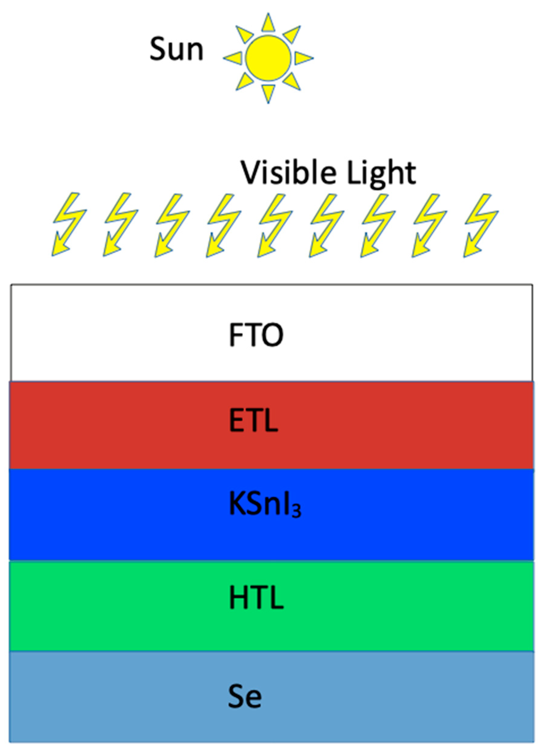
Figure 2.
Crystal structure of the perovskite material KSnI3.
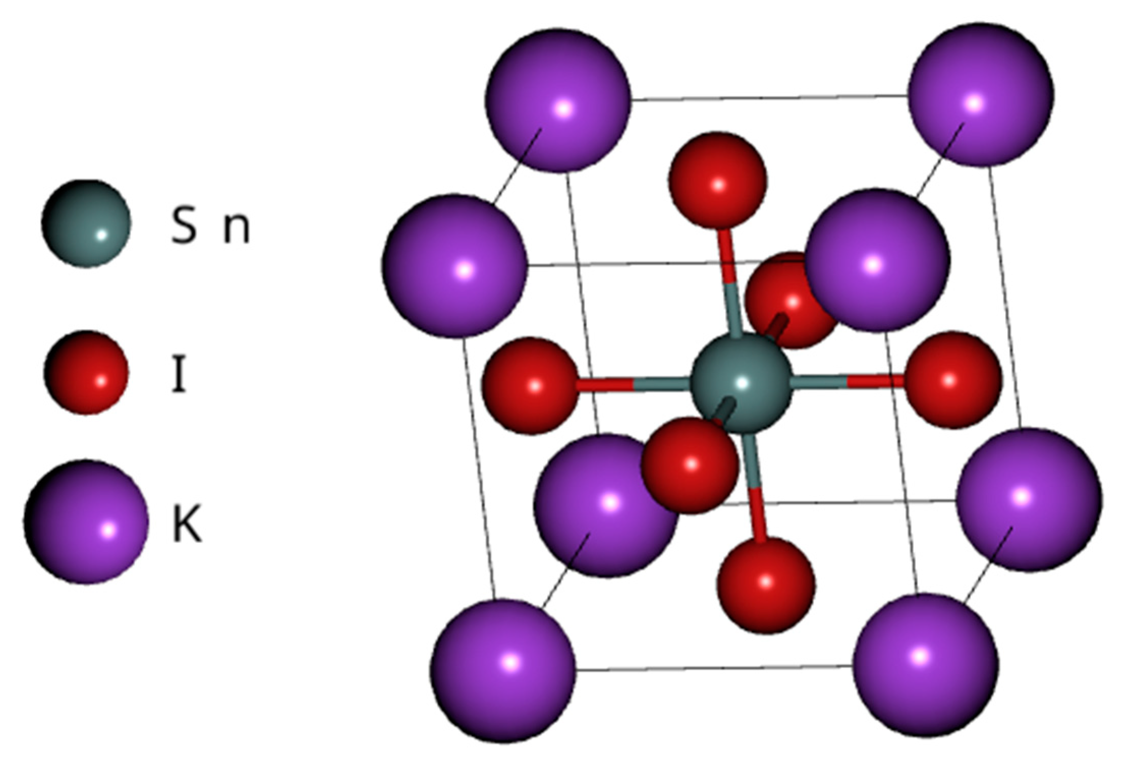
Figure 3.
Energy band diagram of FTO, ETLs, HTL, and KSnI3.
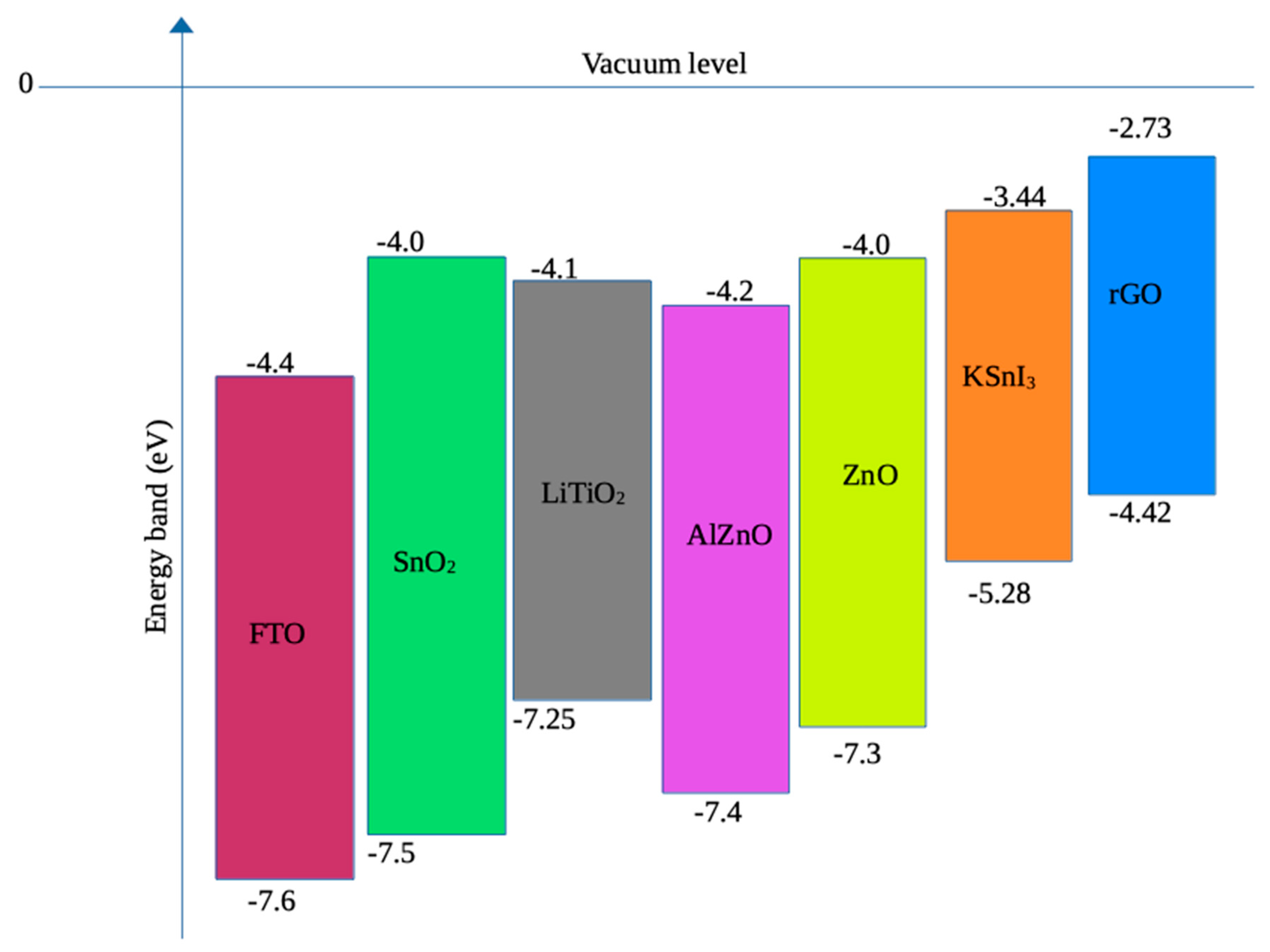
Figure 4.
Dependence of Voc, Jsc, FF, and PCE on rGO thickness.
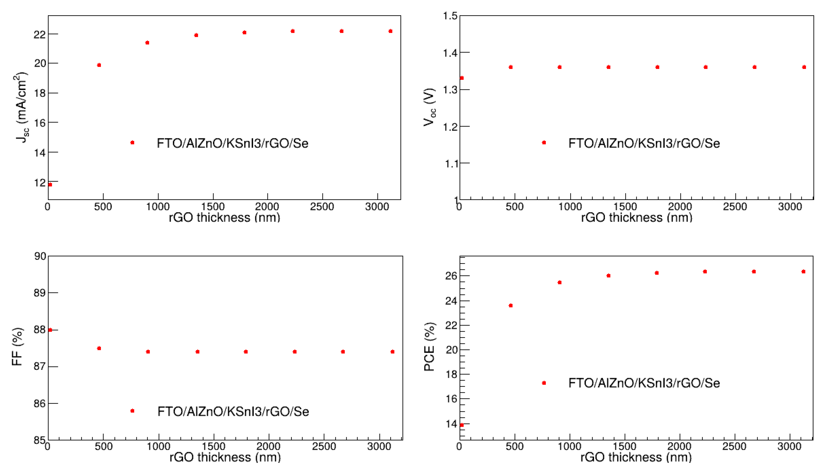
Figure 5.
Voc, Jsc, FF, and PCE as a function of rGO dopant density.
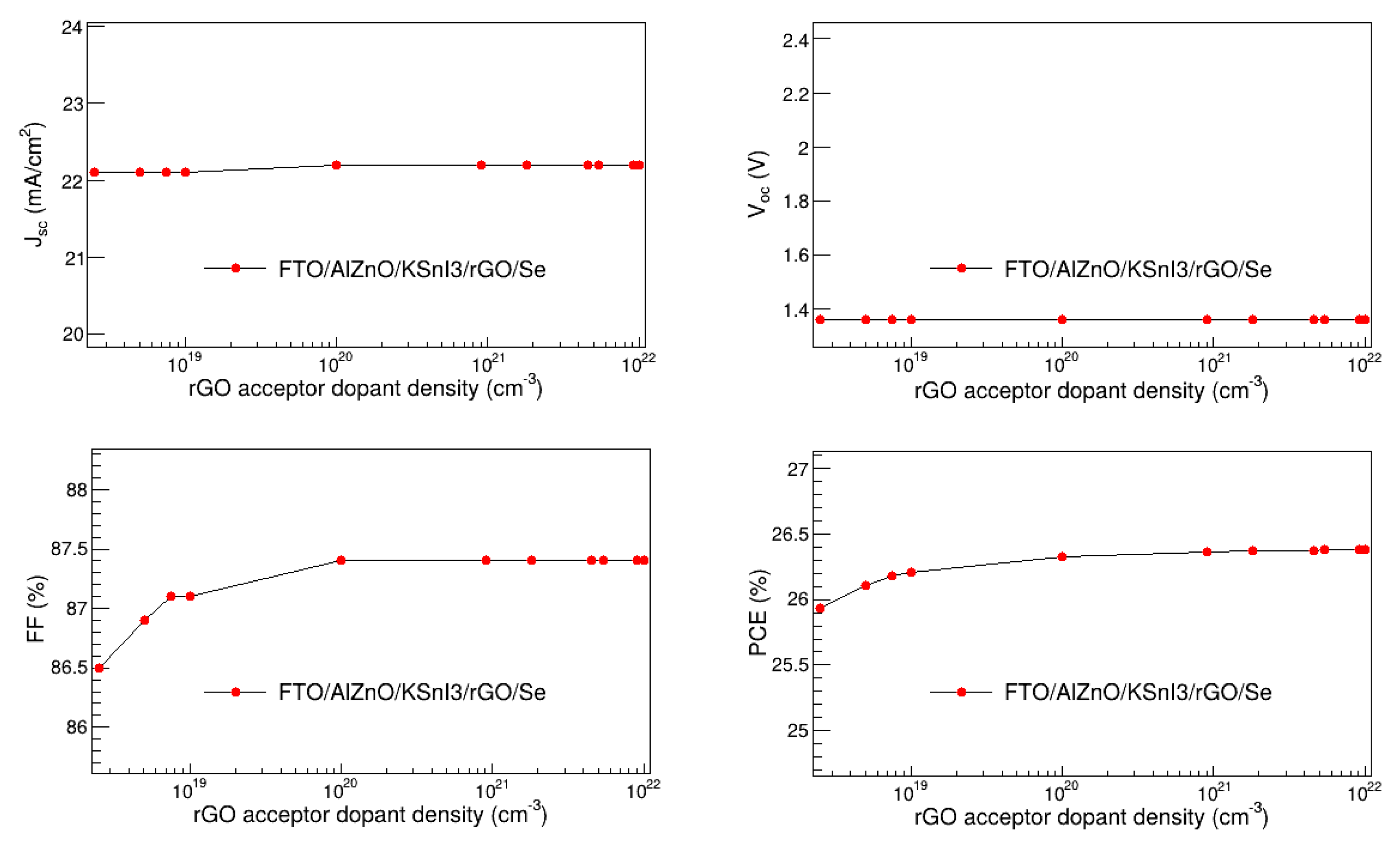
Figure 6.
Voc, Jsc, FF, and PCE as a function of PL thickness.
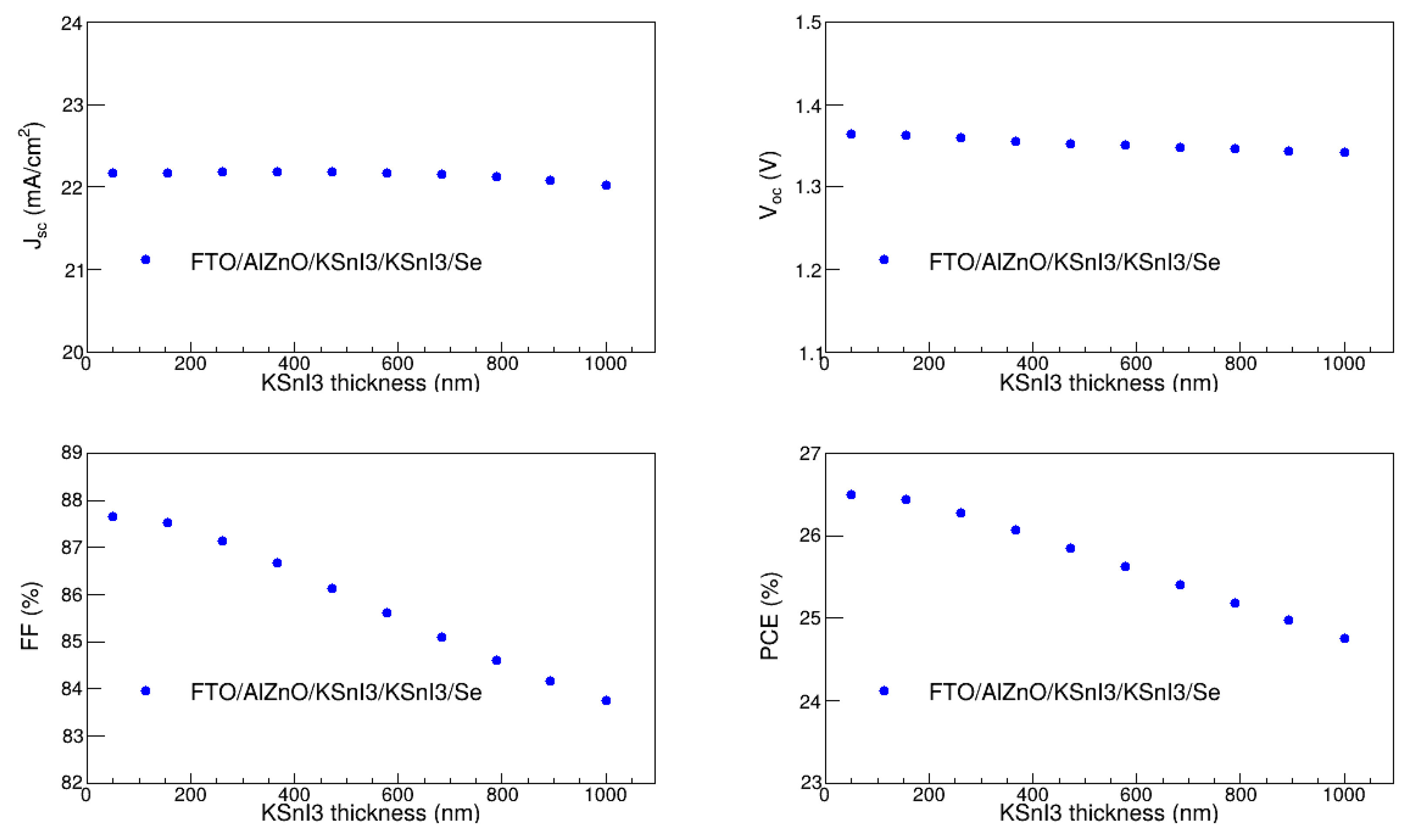
Figure 7.
Voc, Jsc, FF, and PCE as a function of PL acceptor dopant density.
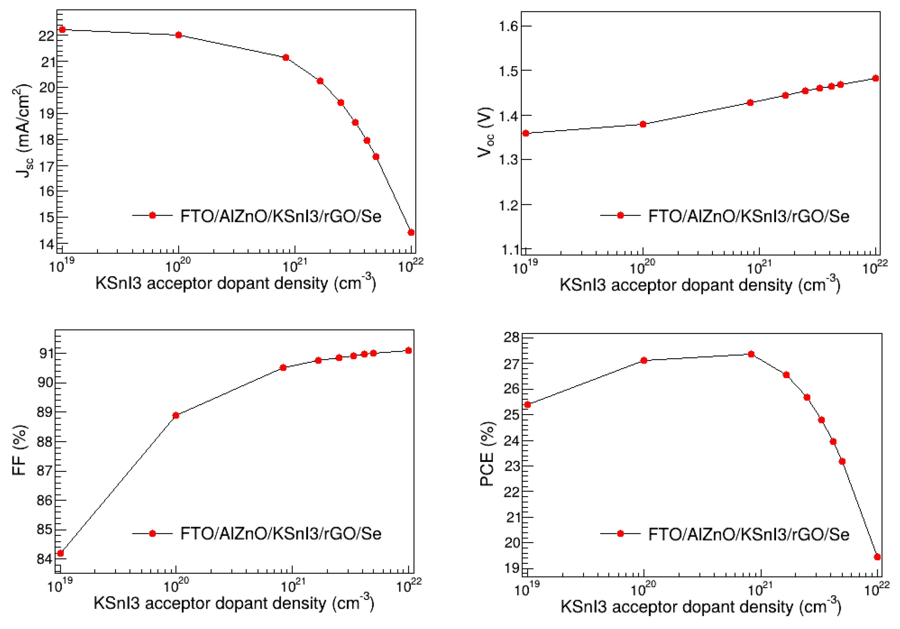
Figure 8.
Voc, Jsc, FF, and PCE as a function of Al-ZnO thickness.
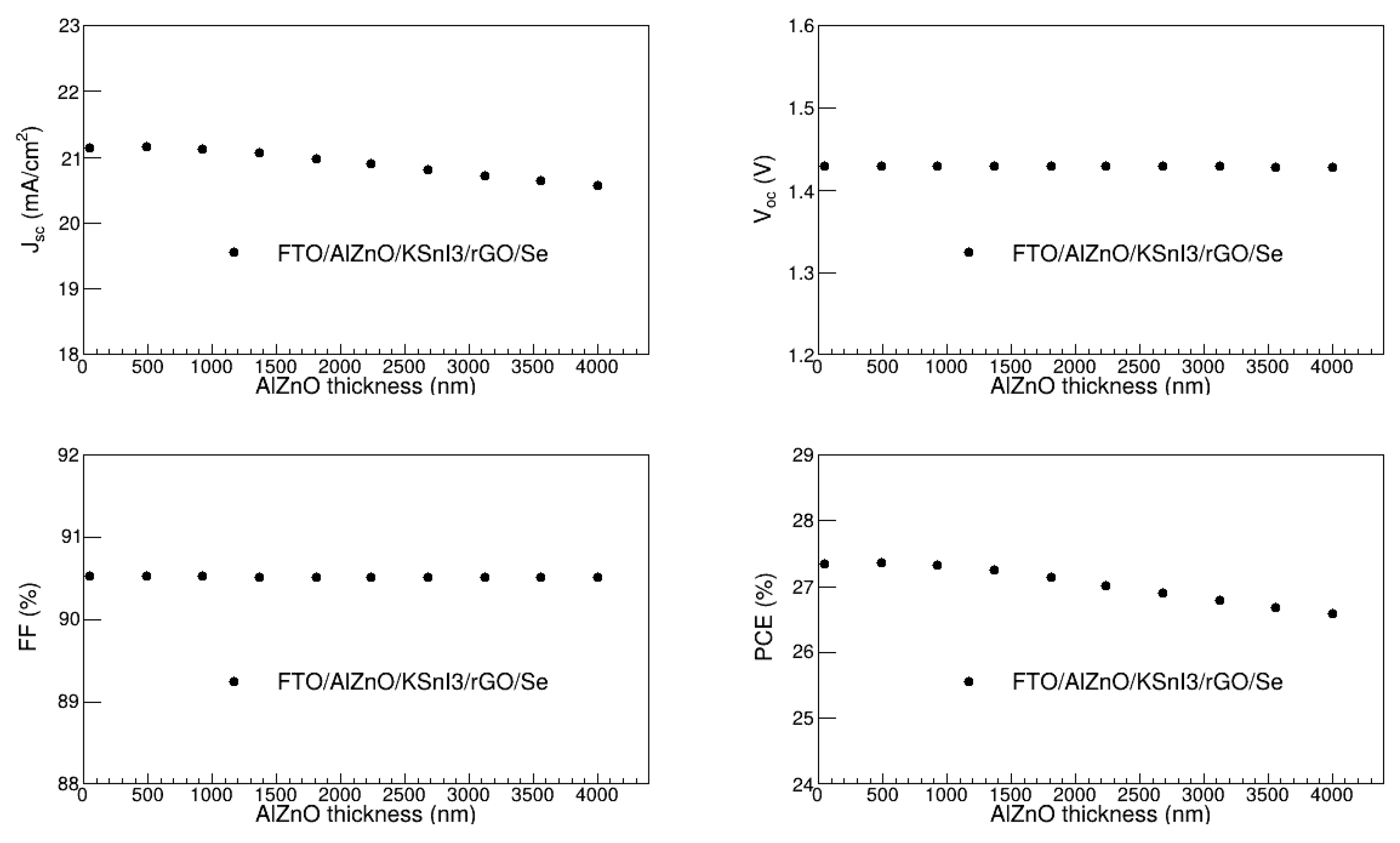
Figure 9.
Voc, Jsc, FF, and PCE as a function of Al-ZnO dopant density.
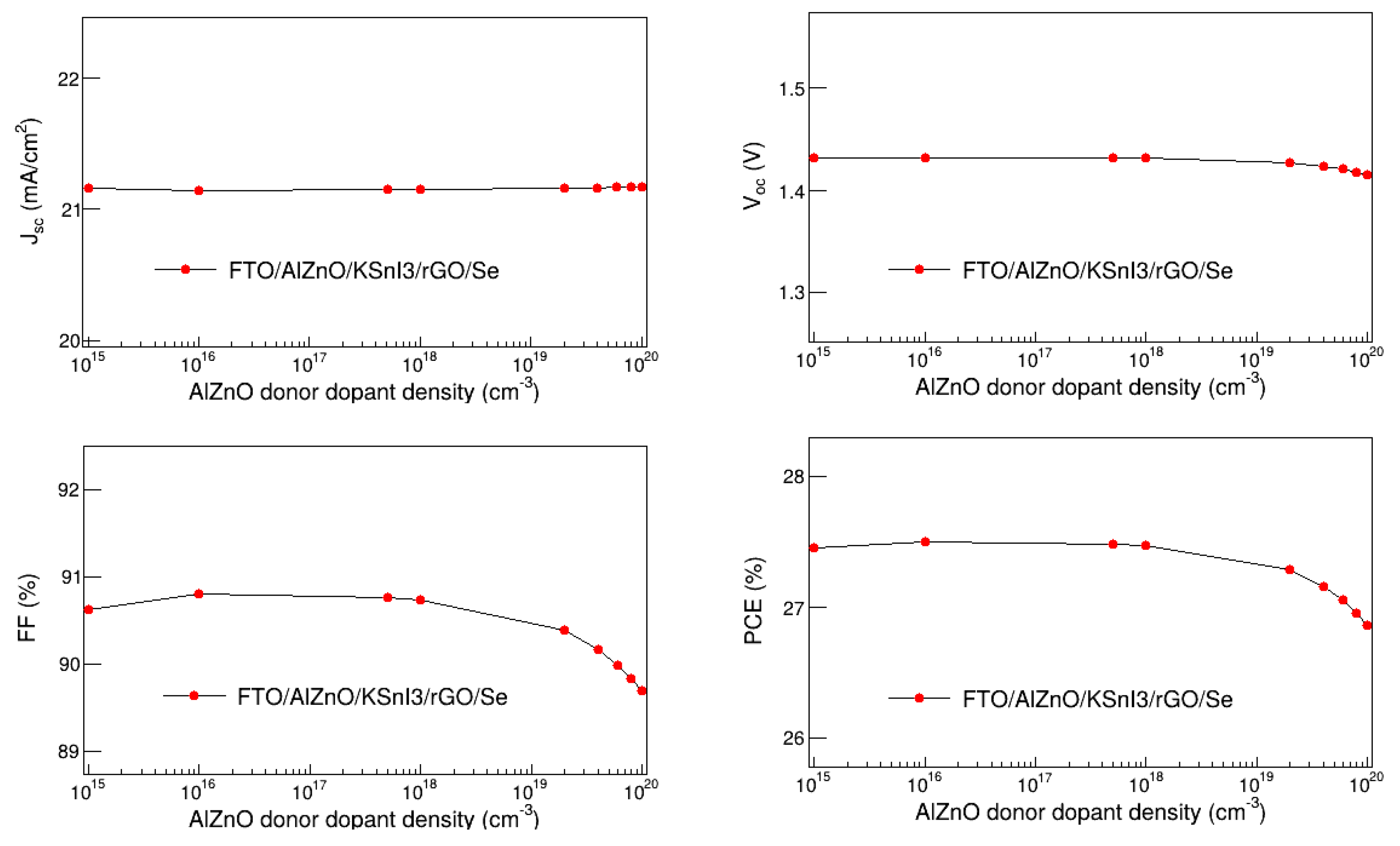
Figure 10.
Voc, Jsc, FF, and PCE as a function of FTO thickness.
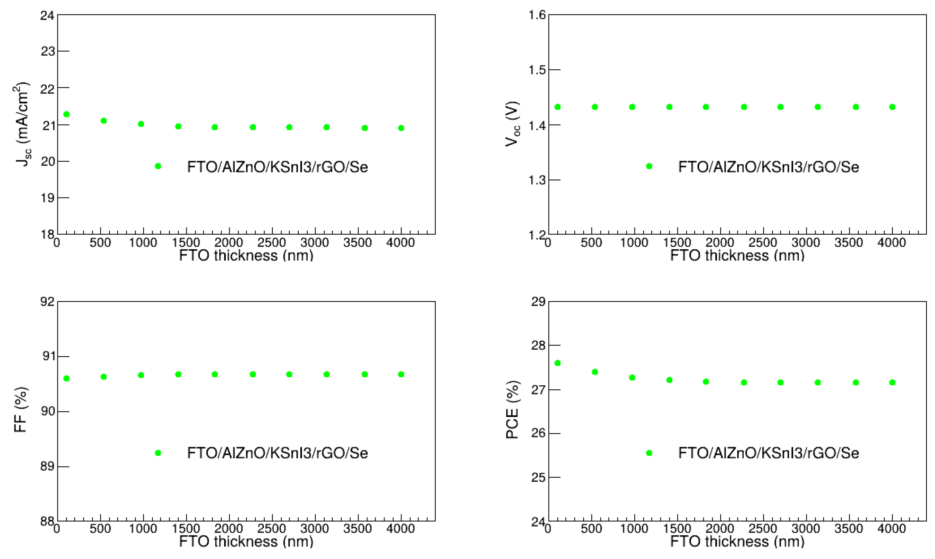
Figure 11.
Voc, Jsc, FF, and PCE as a function of the thicknesses of LiTiO2, ZnO, and SnO2.
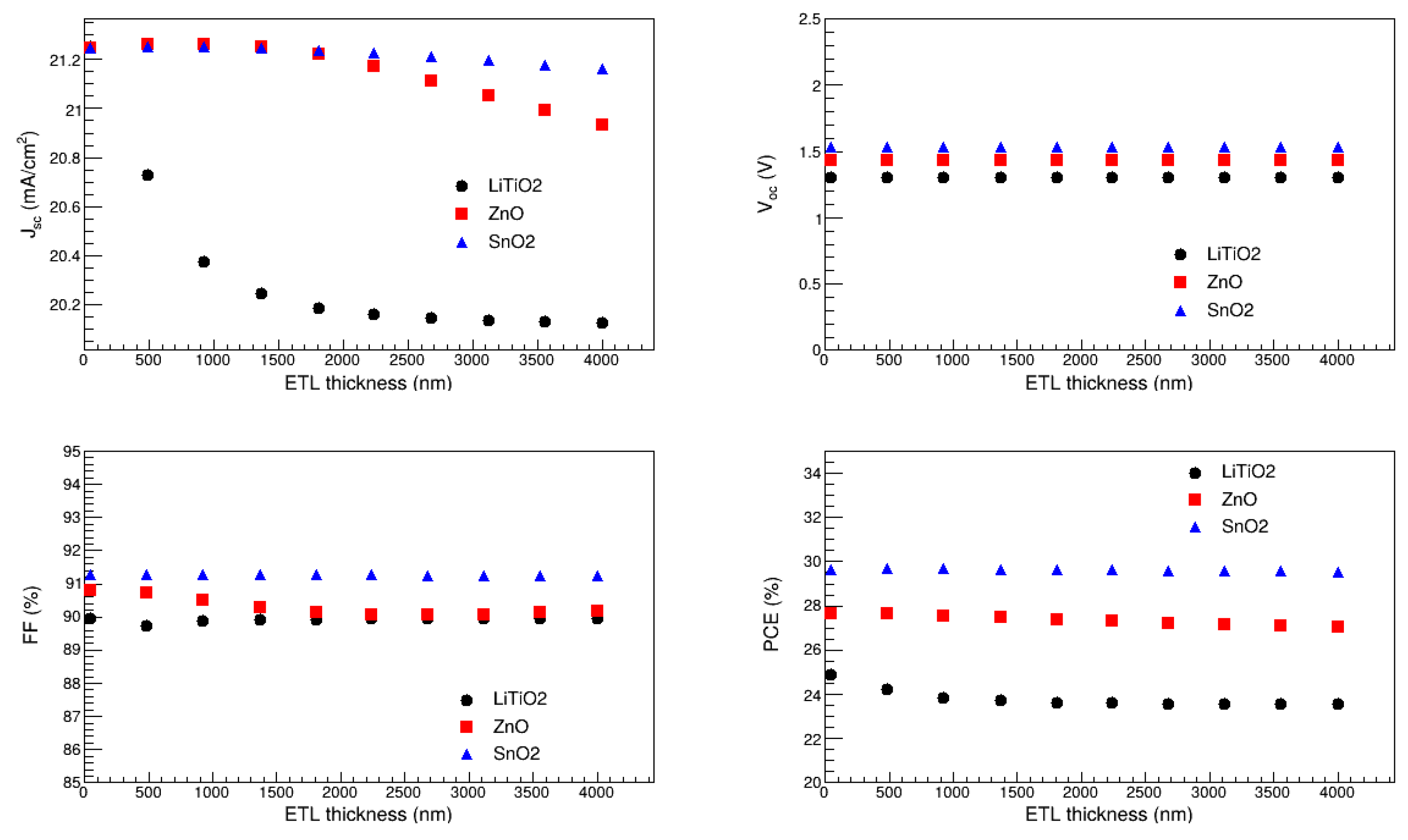
Figure 12.
Voc, Jsc, FF, and PCE as a function of the dopant density of LiTiO2, ZnO, and SnO2.
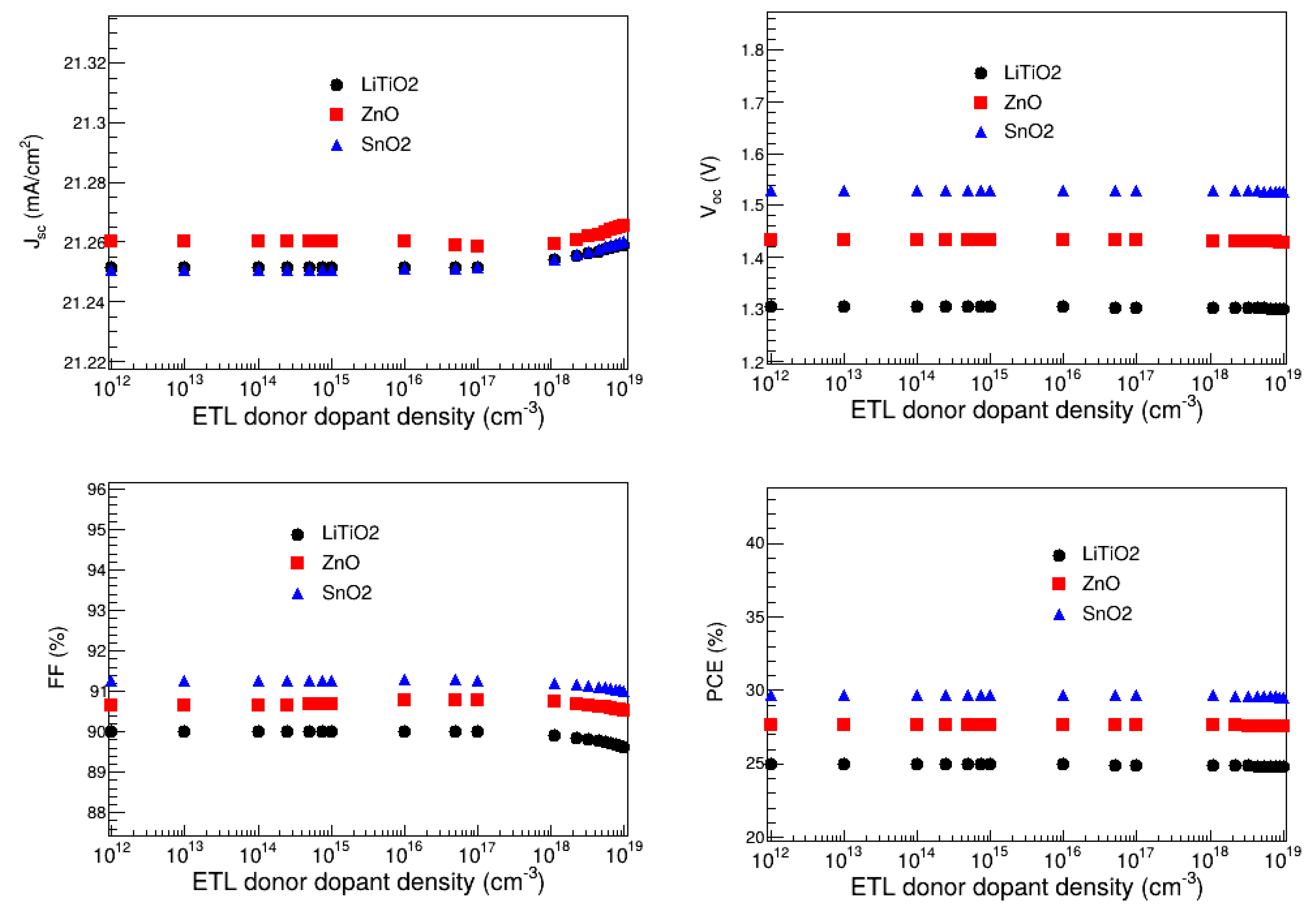
Figure 13.
Voc, Jsc, FF, and PCE as a function of series resistance.
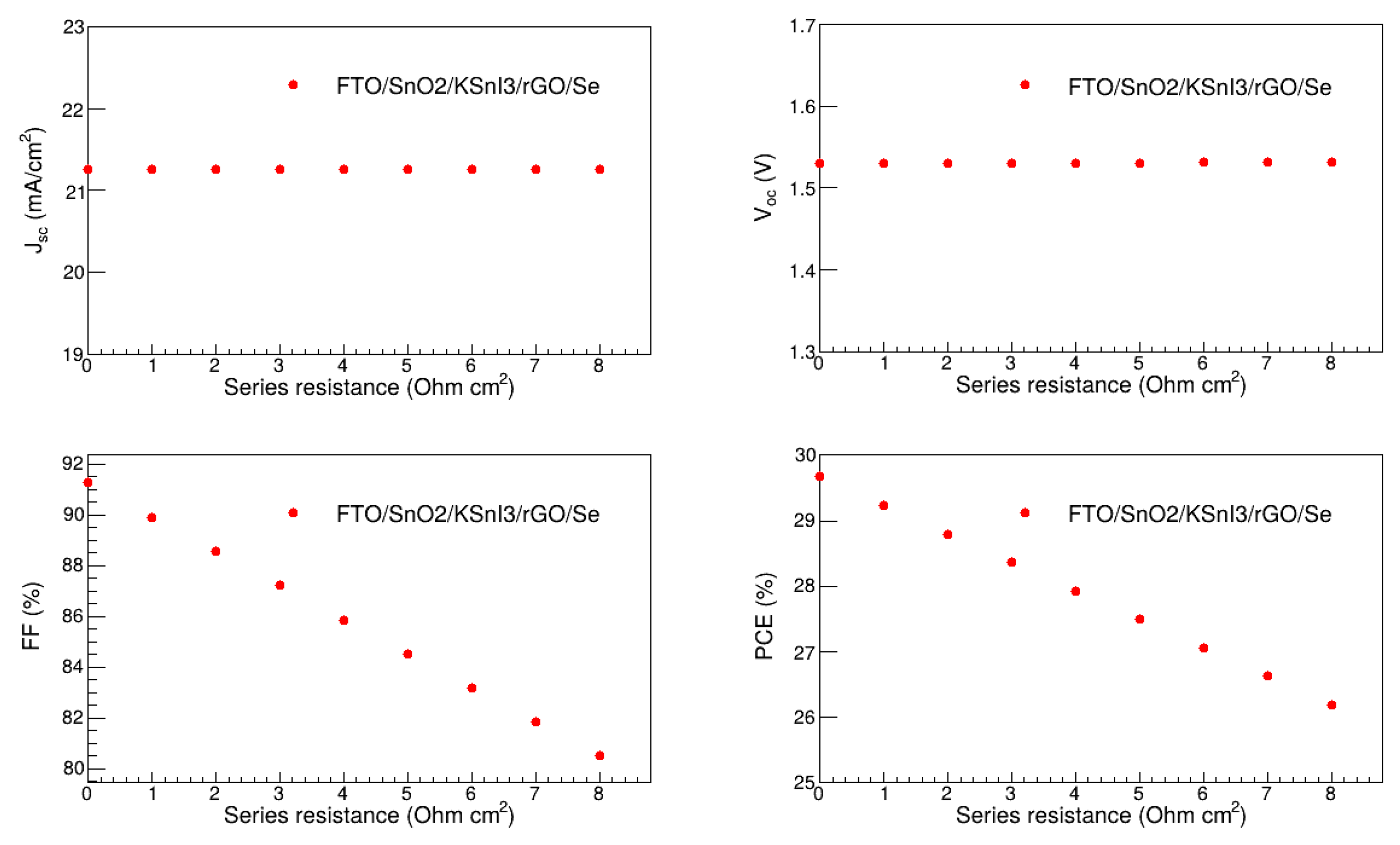
Figure 14.
Voc, Jsc, FF, and PCE as a function of shunt resistance.
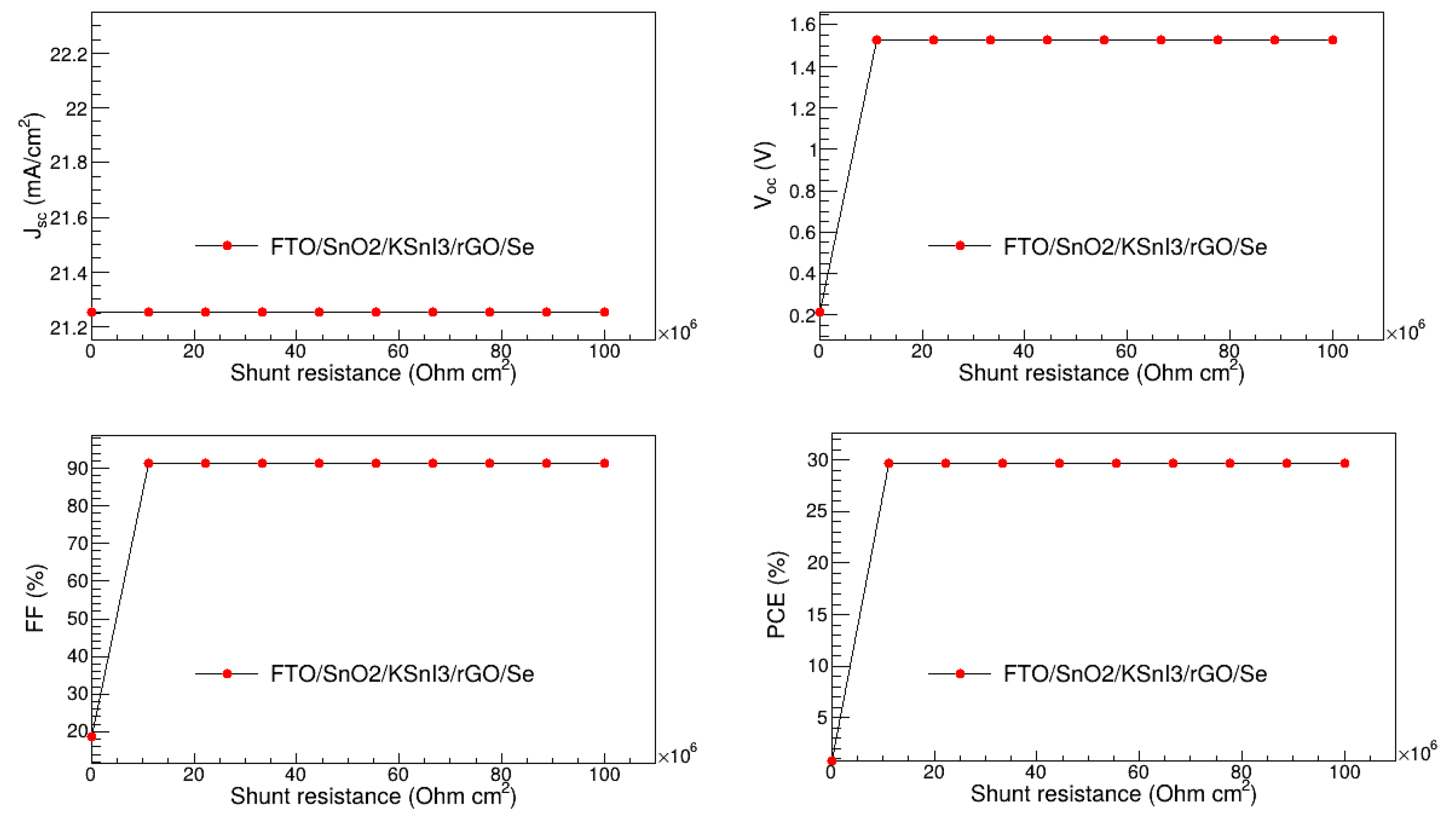
Figure 15.
Voc, Jsc, FF, and PCE as a function of temperature.
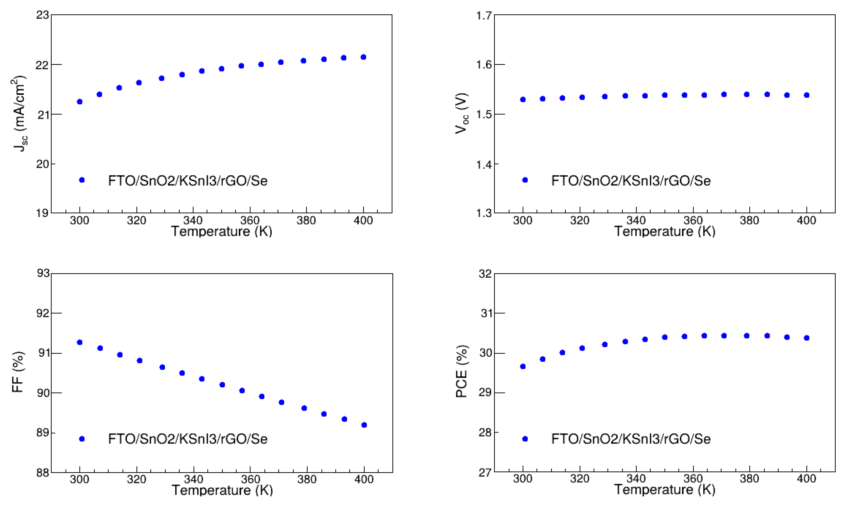

Table 1.
Properties of the KSnI3, ETL, HTL, and FTO used in the simulations before optimization [28,29,30].
| parameters | FTO | Al-ZnO | LiTiO2 | ZnO | SnO2 | KSnI3 | rGO |
| Thickness (nm) | 400 | 400 | 400 | 400 | 400 | 400 | 400 |
| Eg (eV) | 3.5 | 3.1 | 3.15 | 3.28 | 3.5 | 1.84 | 1.69 |
| χ (eV) | 4 | 4 | 4 | 4 | 3.9 | 3.44 | 3.56 |
| εr | 9 | 9 | 13.6 | 9 | 9 | 10.4 | 13.3 |
| Nc (cm-3) | 2.02x10¹⁸ | 2x10¹⁸ | 3x10²⁰ | 2x10¹⁸ | 2.2x10¹⁸ | 2.2x10¹⁸ | 1018 |
| Nv (cm-3) | 1.8x10¹⁹ | 1.8x10¹⁹ | 2x10²⁰ | 1.8x10¹⁹ | 1.8x10¹⁹ | 1.8x10¹⁹ | 1.8x10¹⁹ |
| Vth,n (cm s-1) | 107 | 107 | 107 | 107 | 107 | 107 | 107 |
| Vth,h (cm s-1) | 107 | 107 | 107 | 107 | 107 | 107 | 107 |
| μn (cm2/V/s) | 2x101 | 13.84 | 30 | 43 | 200 | 21.28 | 2.6x101 |
| μp (cm2/V/s) | 1x10⁻¹ | 25 | 0.01 | 25 | 80 | 19.46 | 1.23x10² |
| NA (cm-3) | 0 | 0 | 0 | 0 | 0 | 1x10¹⁶ | 1022 |
| ND (cm-3) | 2x10¹⁹ | 1.02x10¹⁹ | 2x10¹⁷ | 2.9x10¹⁵ | 1x10¹⁷ | 1x10¹⁵ | 0 |
| Nt (cm-3) | 1015 | 1015 | 1014 | 1015 | 1015 | 1015 | 1014 |
| Interface | HTL/KSnI3 | ETL/KSnI3 |
| Defect type | Neutral | Neutral |
| Energetic distribution | Single | Single |
| Capture cross-section for electrons (cm-2) | 10-19 | 10-19 |
| Capture cross-section for holes (cm-2) | 10-19 | 10-19 |
| Reference for defect energy level | Above VB maximum | Above VB maximum |
| Energy with respect to reference (eV) | 0.6 | 0.6 |
| Total density (cm-3) | 1x10¹⁰ | 1x10¹⁰ |
Table 3.
Properties used in the benchmark simulation of FTO/SnO2/3C-SiC/KSnI3/NiO/C PSC [28] .
Table 3.
Properties used in the benchmark simulation of FTO/SnO2/3C-SiC/KSnI3/NiO/C PSC [28] .
| parameters | FTO | SnO2 | 3C-SiC | KSnI3 | NiO |
| Thickness (nm) | 500 | 25 | 20 | 1500 | 20 |
| Eg (eV) | 3.2 | 3.5 | 2.36 | 1.84 | 3.8 |
| χ (eV) | 4 | 3.9 | 3.8 | 3.44 | 1.4 |
| εr | 9 | 9 | 9.72 | 10.4 | 10.7 |
| Nc (cm-3) | 2.2x10¹⁸ | 2.2x10¹⁸ | 1.553x10¹⁹ | 2.2x10¹⁸ | 2.5x10¹⁹ |
| Nv (cm-3) | 1.8x10¹⁸ | 1.8x10¹⁹ | 1.163x10¹⁹ | 1.8x10¹⁹ | 2.8x10¹⁹ |
| Vth,n (cm s-1) | 107 | 107 | 107 | 107 | 107 |
| Vth,h (cm s-1) | 107 | 107 | 107 | 107 | 107 |
| μn (cm2/V/s) | 2x101 | 200 | 900 | 21.28 | 12 |
| μp (cm2/V/s) | 1x101 | 80 | 40 | 19.46 | 28 |
| NA (cm-3) | 0 | 0 | 0 | 1x10¹⁶ | 1x10¹⁹ |
| ND (cm-3) | 2x10¹⁹ | 1x10²⁰ | 1x10²⁰ | 1x10¹⁵ | 0 |
| Nt (cm-3) | 1014 | 1015 | 1014 | 1014 | 1015 |
Table 4.
Benchmark results for the FTO/SnO2/3C-SiC/KSnI3/NiO/C configuration.
| PSC structure | Voc (V) | Jsc (mA/cm2) | FF (%) | PCE (%) | Reference |
| FTO/SnO2/3C-SiC/KSnI3/NiO/C | 1.399 | 17.72 | 89.99 | 22.31 | This work |
| FTO/SnO2/3C-SiC/KSnI3/NiO/C | 1.392 | 18.27 | 89.57 | 22.78 | Ref. [28] |
Table 5.
Optimized parameters of FTO, ETLs, HTL, and KSnI3 for the four optimized PSC structures.
| parameters | FTO | Al-ZnO | LiTiO2 | ZnO | SnO2 | KSnI3 | rGO |
| Thickness (nm) | 100 | 489 | 50 | 489 | 489 | 50 | 2670 |
| NA (cm-3) | 8.33x10²⁰ | 5.45x10²¹ | |||||
| ND (cm-3) | 1015 | 1012 | 1016 | 1016 |
Table 6.
The Voc, Jsc, FF, and PCE of the optimized PSC configurations.
| PSC structure | Voc (V) | Jsc (mA/cm2) | FF (%) | PCE (%) |
| FTO/Al-ZnO/KSnI3/rGO/Se | 1.44 | 21.28 | 90.15 | 27.60 |
| FTO/LiTiO2/KSnI3/rGO/Se | 1.30 | 21.25 | 90.01 | 24.94 |
| FTO/ZnO/KSnI3/rGO/Se | 1.43 | 21.26 | 90.70 | 27.62 |
| FTO/SnO2/KSnI3/rGO/Se | 1.53 | 21.25 | 91.27 | 29.67 |
Table 7.
The Voc, Jsc, FF, and PCE of the optimized FTO/SnO2/KSnI3/rGO/Se when optimal Rs, Rsh, and temperature are assumed.
Table 7.
The Voc, Jsc, FF, and PCE of the optimized FTO/SnO2/KSnI3/rGO/Se when optimal Rs, Rsh, and temperature are assumed.
| PSC structure | Voc (V) | Jsc (mA/cm2) | FF (%) | PCE (%) |
| FTO/SnO2/KSnI3/rGO/Se | 1.54 | 22.04 | 89.76 | 30.44 |
Table 8.
Performance metrics of the optimized PSC structures and literature.
| PSC structure | PCE (%) | Reference |
| FTO/Al-ZnO/KSnI3/rGO/Se | 27.16 | This work |
| FTO/LiTiO2/KSnI3/rGO/Se | 24.94 | This work |
| FTO/ZnO/KSnI3/rGO/Se | 27.62 | This work |
| FTO/SnO2/KSnI3/rGO/Se | 30.44 | This work |
| FTO/TiO2/KSnI3/Spiro-OMeTAD/W | 9.776 | [23] |
| FTO/C60/KSnI3/PTAA/C | 10.83 | [24] |
| FTO/TiO2/KSnBr3/Cu2O/Au | 8.05 | [39] |
| FTO/F16CuPc/KSnI3/CuPc/C | 11.91 | [25] |
| FTO/ZnOS/KSnI3/NiO/C | 9.28 | [26] |
| FTO/ZnO/KSnI3/CuI/Au | 20.99 | [27] |
| FTO/SnO2/3C–SiC/KSnI3/NiO/C | 22.78 | [28] |
Disclaimer/Publisher’s Note: The statements, opinions and data contained in all publications are solely those of the individual author(s) and contributor(s) and not of MDPI and/or the editor(s). MDPI and/or the editor(s) disclaim responsibility for any injury to people or property resulting from any ideas, methods, instructions or products referred to in the content. |
© 2025 by the authors. Licensee MDPI, Basel, Switzerland. This article is an open access article distributed under the terms and conditions of the Creative Commons Attribution (CC BY) license (http://creativecommons.org/licenses/by/4.0/).
Copyright: This open access article is published under a Creative Commons CC BY 4.0 license, which permit the free download, distribution, and reuse, provided that the author and preprint are cited in any reuse.


