Submitted:
14 March 2025
Posted:
17 March 2025
Read the latest preprint version here
Abstract
The rapid development of electronic technology has generated the demand for low - power and high- performance circuit design. The key indicator, power supply rejection ratio (PSRR), is crucial for circuit design. Given the deficiencies of existing PSRR calculation methods in high-frequency applications and complex circuit designs, this pa-per proposes an innovative PSRR calculation theory. Based on a simplified circuit model, this theory uses Thevenin's equivalent principle to transform multi-stage operational amplifiers into a black-box model, simplifying the calculation process and enhancing the intuitiveness of calculation. In view of the characteristics of industrial design, we also proposed the PSR Gain Bandwidth (PGB) theory, which can more intuitively analyze the trade-off between PSRR and other performance within the target range. This paper further explores the impact of different circuit structures on PSRR characteristics, covering typical circuit structures such as PMOS/NMOS input two-stage operational amplifiers and folded cascode operational amplifiers, and deeply analyzes the key factors affecting PSRR characteristics. The effectiveness of the proposed theory is verified through case analysis, and its potential applications in circuit designs with high PSRR requirements are demonstrated.
Keywords:
PGB
; op-amps
; PSRR
; Thevenin Equivalence
1. Introduction
The swift advancement of electronic technology has given rise to the necessity for low-power and high-performance circuit design [1,2,3,4]. In this context, fundamental building blocks of any chip, such as operational amplifiers, low-dropout regulators (LDOs), and bandgap references, have become increasingly important. Maintaining circuit stability under diverse operating conditions thus becomes critical. The PSRR serves as a key metric for assessing a circuit’s ability to suppress power supply noise, directly impacting signal integrity and system stability. In the realm of high-precision medical devices [5], enhancing the PSRR augments measurement precision and diagnostic reliability. In high-speed communication systems, it attenuates noise interference during data transmission. And in portable devices, it prolongs battery life and enhances immunity to interference.
Conventional PSRR calculation methods rely predominantly on simplified analyses of system poles and zeros, often using low-frequency equivalent circuit models. However, as circuits operate at higher frequencies, parasitic capacitance, inductance, and other high-frequency effects introduce significant deviations between calculated and actual performance. This discrepancy becomes even more pronounced in radio frequency (RF) and high-speed communication circuits, where complex interactions between power supply noise and parasitic parameters exacerbate the issue. Moreover, existing methods lack a unified theoretical framework and standardized calculation process, forcing designers to invest substantial time in theoretical derivation and experimental validation when addressing novel circuit architectures. Such constraints hinder design efficiency and innovation.
To overcome these challenges, we propose a novel PSRR calculation theory. Our approach evaluates the PSRR of a two-stage operational amplifier by modeling the first stage as a black box with defined input and output. We apply the Thevenin equivalent model to capture the internal behavior of the first stage and reintegrate this result into the overall circuit model. This strategy simplifies the calculation and enhances its intuitiveness. In addition, the proposed theory offers a detailed description of key parameters—including poles, zeros, and gain bandwidth.
Furthermore, industrial design pays more attention to the analysis of power supply rejection ratio (PSR). Since it involves complex S-parameter models, it is difficult to optimize it directly. This paper proposes a simplified evaluation method based on PGB, which avoids the tedious S-parameter calculation by directly extracting PSRR and first-order pole characteristics, thereby achieving efficient and intuitive PSR performance prediction within the target frequency band. This method shows universality before the gain-bandwidth product (GBW), and can uniformly explain the phenomenon that different circuit architectures (such as LDO) have differentiated UGB-level PSR characteristics under the same low-frequency PSR and pole configuration.
We validate the proposed method by analyzing typical circuit structures. The rest of this paper is organized as follows. Section II reviews the traditional PSRR calculation methods and introduces the theoretical basis of our method and details the PSRR calculation process and zero-pole characteristics of different circuits. Section III verifies the accuracy of PSRR calculation through the design and simulation of complex circuits and confirms the feasibility of optimizing PSRR through PGB calculation analysis. Finally, Section IV summarizes the advantages of the proposed method and outlines the direction of future research.
2. Materials and Methods
2.1. Related Work
Razavi introduced a small-signal model–based method for PSRR calculation [6]. This approach works well for simple and symmetric circuits by directly computing PSRR through the analysis of small-signal gain:
where Adm denotes the differential gain and A represents the overall gain of the small-signal model.
However, as circuit designs become more complex, especially with asymmetric or multistage circuits, the limitations of this method become evident. The extended method proposed by Grey [7] is theoretically more complete but suffers from cumbersome calculation procedures and unvalidated suitability for high-frequency circuits.
PSRR computation is influenced by the characteristics of the input, intermediate, and output stages of a two-stage operational amplifier. For instance, the bias current, input impedance, and offset voltage at the input stage significantly affect PSRR; circuits designed with low bias current and high input impedance tend to exhibit improved PSRR. In the intermediate stage, higher gain amplifies power supply noise, thereby reducing PSRR. Similarly, the output stage must be designed to balance driving capability with noise suppression to maintain a high PSRR.
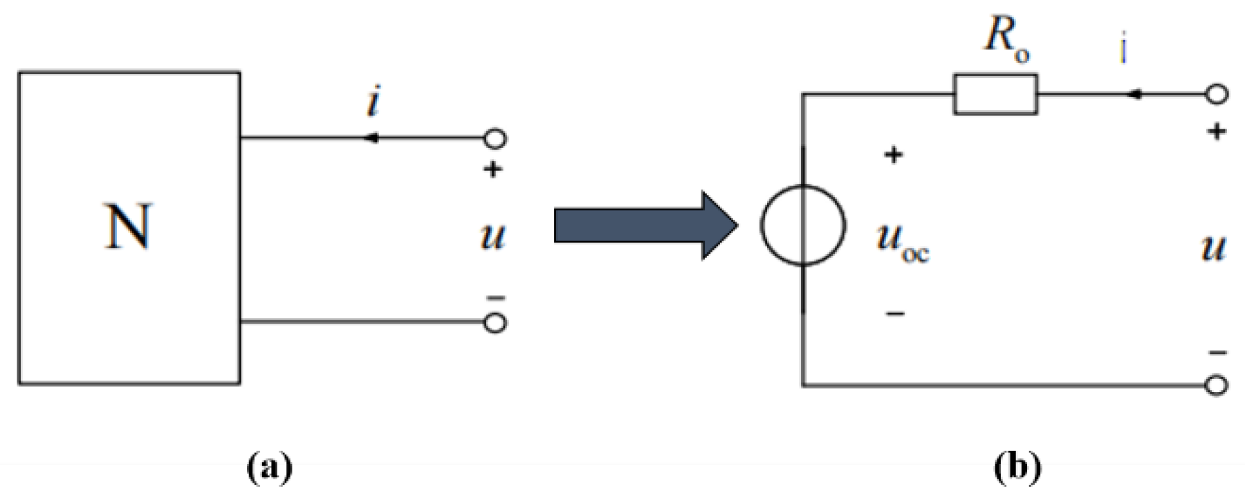
To tackle the challenges associated with complex circuit analysis, we leverage Allen's interpretation of PSRR [8] and develop a "black-box" model that simplifies the intricate circuitry. This model is particularly applicable to Thevenin Equivalent Circuit Analysis, where the Thevenin theorem simplifies linear resistor networks with independent sources into a single voltage source in series with a resistance. Specifically, for any single-port network N, the port can be represented equivalently by a voltage source —whose value corresponds to the open-circuit voltage (Vo)—in series with a resistance Ro, which is the equivalent resistance observed at the port when all independent sources are deactivated.
Figure 1.
Thevenin equivalent circuit.
2.2. Proposed Methodology
In this section, we employ the black-box theory proposed in the previous chapter to analyze the PSRR of various operational amplifiers.
2.2.1. PSRR Calculation for P-Input Two-Stage Op-Amps
Figure 2.
Typical structure of a P-input two-stage op-amp.
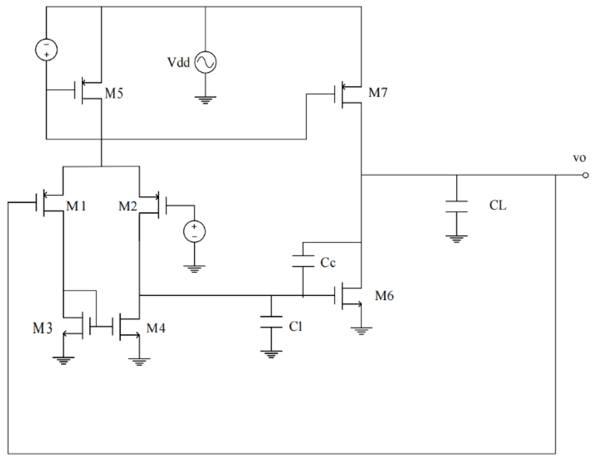
In this op-amp, the input stage usually consists of two P-type MOSFETs (M1 and M2) that receive the input signal and provide initial amplification. Transistors M3 and M4 act as load devices and work in conjunction with M1 and M2 to enhance the gain of the input stage. Current mirrors comprising M5 and M7 supply a stable bias current to the input stage while ensuring that the currents in M1 and M2 are matched. In the output stage, transistor M6 further amplifies the signal from the input stage and provides sufficient drive capability for the load.
To simplify the calculation, we treat the first stage of the op-amp as a “black box” with input terminals which denoted as and an output terminal which denoted as . This is illustrated in Figure 3.
The processing of the first stage is performed in several steps:
- (a)
- Evaluating the Impact of Vdd on the Thevenin Equivalent Output Voltage of the First Stage
Figure 4.
Thevenin equivalent circuit for the first stage of the op-amp.
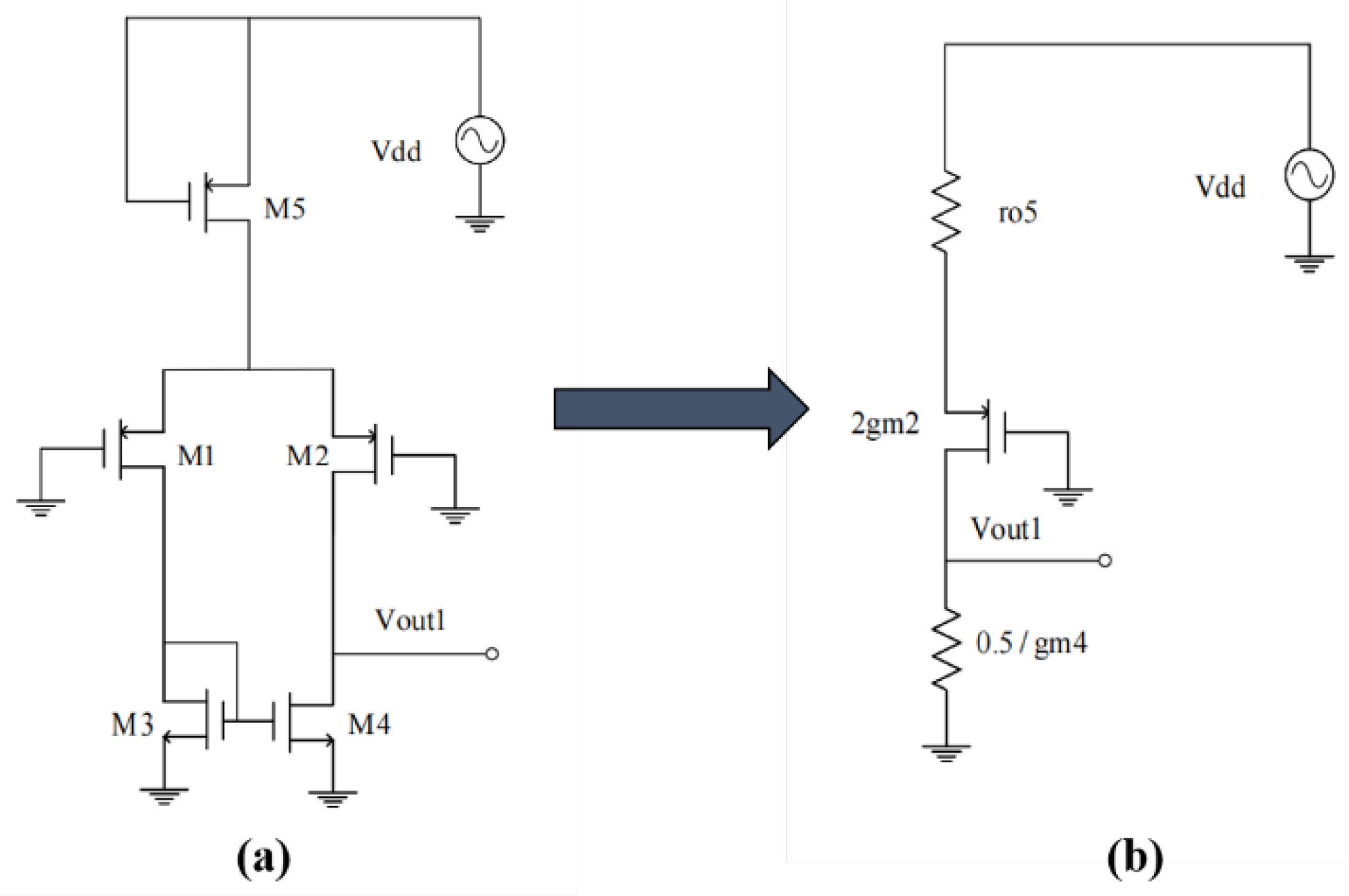
The first stage is viewed as an independent module. Based on the Thevenin theorem, the equivalent voltage generated by is given by .
- (b) Evaluating the Impact of Vin on the Thevenin Equivalent Output Voltage of the First Stage
Figure 5.
Thevenin equivalent output voltage of the first stage.
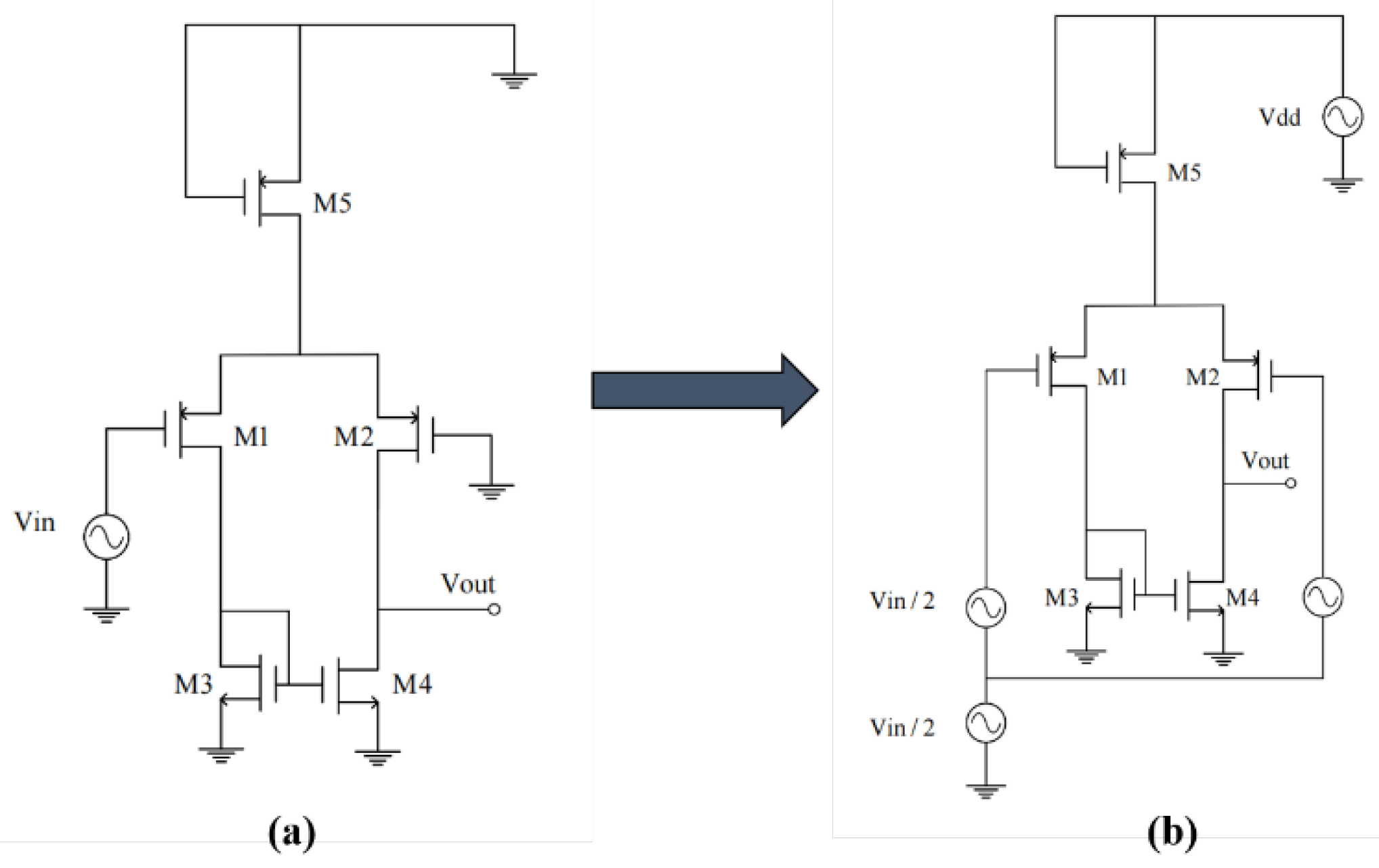
For a differential input , the corresponding Thevenin equivalent output voltage is:
Likewise, for a common-mode input , the corresponding Thevenin equivalent output voltage is:
The common-mode output voltage is relatively small and can be combined with the differential output voltage. Therefore, in the subsequent calculations, the common-mode contribution is typically neglected.
- (c) Constructing the Thevenin Equivalent Circuit
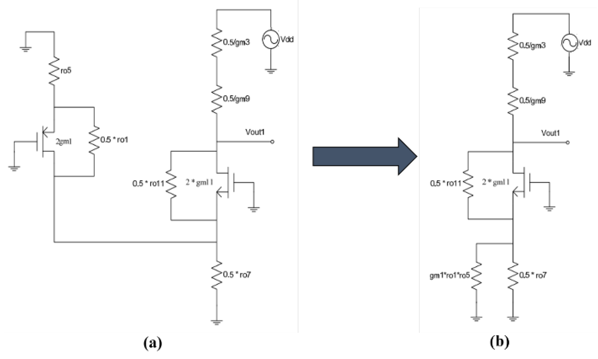
Using the superposition theorem, the first stage is further simplified to a structure consisting of a voltage source and a resistor, as shown in the lower left area of Figure 6, where represents the output resistance of the first stage.
- (a)
- Deriving the PSRR Transfer Function
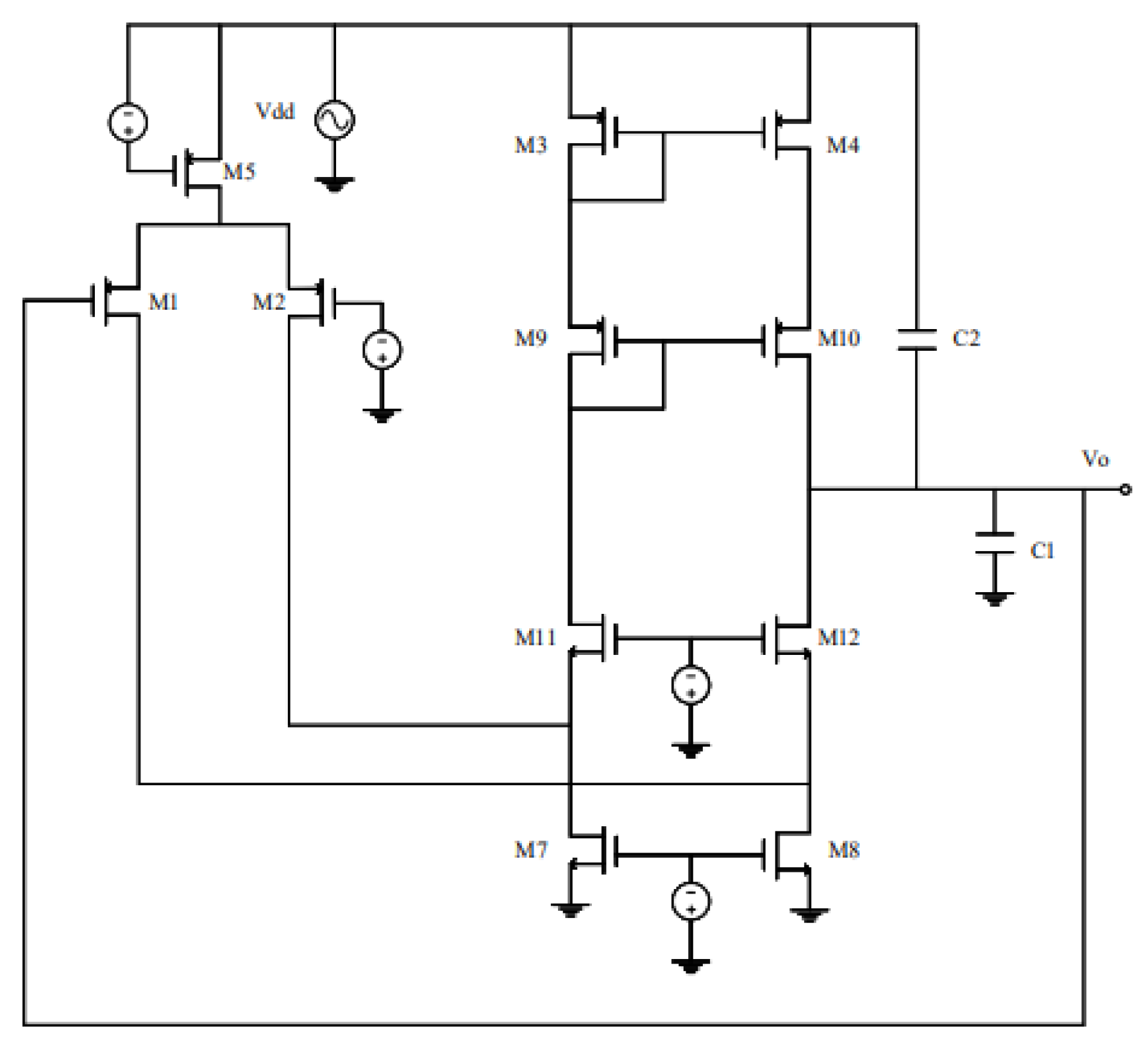
The equivalent circuit for the two-stage op-amp is shown in Figure 7. Considering the gate-drain capacitance Cgd of M7, we use small-signal analysis to write the node current equations and thereby solve for the PSRR transfer function.
First, we write the node current equation at node :
Similarly, writing the node current equation at node :
By equating (5) and (7):
In the derivation above, it is assumed that , due to matching requirements. if we set and ,we obtain that , , and:
Next, we derive the DC PSRR value as well as the positions of the zero and pole:
Assuming , and for stability, we have :
Further assuming , leads to:
The location of is the closest to the origin relative to the first pole. Whether the DC PSRR value is positive or negative depends on the specific values of N and M When N is approximately twice that of M, the DC PSRR value becomes very high; however, the zero also shifts closer to the origin.
The PSRR is influenced by two signal paths within the op-amp. In the first path, the signal entering from reduces the output voltage at low frequencies; in the second path, the signal entering from has the opposite effect and increases the output voltage. For simplification, the drain of M5 is grounded, thereby neglecting the signal contribution from M5 and resulting in a positive DC PSRR gain. Under ideal bias current source conditions, if N is greater than twice that of M, the PSRR is negative; if N is less than twice that of M, the PSRR is positive. The location of the zero is also closely related to the ratio of these two parameters.
PGB (PSR Gain Bandwidth):
By approximating the PSRR curve as having a single zero, and drawing an analogy with the gain-bandwidth product in op-amps, we define PGB as the product of the zero frequency and the DC PSRR value:
According to (18), when the PGB value is large, the −20 dB/dec asymptote of the main zero shifts further away from the origin while maintaining its slope, thereby improving the frequency characteristics in the BE segment. If, while keeping other parameters constant, a parameter is adjusted so that it approaches 2M, the DC PSRR value increases significantly and the zero moves toward the origin, optimizing the frequency response in the CL segment. If the frequency of interest falls on the DE segment of the curve, the impact of the parameter change is relatively small. As shown in Figure 8, curve CDE represents the original PSRR response, while curve ABE corresponds to the frequency response after a parameter adjustment.
This process bears some similarity to considerations of the loop bandwidth (GB) of the two-stage op-amp. Increasing a particular parameter directly enhances the DC PSRR value, which is beneficial for our analysis. Under stability constraints, reducing the parameter Cc shifts outward, thereby improving the frequency response; similarly, increasing shifts the BE line outward; increasing and directly optimizes the DC PSRR value; while increasing and raises the DC PSRR value but also moves closer to the origin, benefiting only the low-frequency response—the PGB remains unchanged, and hence the improvement for high frequencies is limited. However, since the bandwidth that the industry is concerned about is usually low-frequency, PGB can play a vital role in the design of specific field.
2.2.1. PSRR Calculation for N-Input Two-Stage Op-Amps
In this subsection, we adopt a similar analytical approach to study the PSRR of N-input two-stage op-amps and thereby demonstrate the portability of the new PSRR calculation theory.
Based on the analysis in Section A for a typical P-input two-stage op-amp, we consolidate the simplified flowchart for a common N-input two-stage op-amp into a single diagram, as shown in Figure 9.
The following quantities are computed: the Thevenin equivalent voltage due to from the first stage, the Thevenin equivalent voltage due to , the PSRR, the DC PSRR value, the zero, the pole, and the PGB.
From Figure 9(b), the Thevenin equivalent voltage due tois given by . While:
Similarly, the Thevenin equivalent voltage due to is :
Using the node current equations, we obtain
Equating (21) and (22) yields:
PSRR Calculation:
Under the assumptions that ,, approximate expressions for the DC PSRR value and the zero can be derived as
Assuming that ,,, , he pole of the PSRR is approximately given by:
Similarly, the calculation of PGB follows the same procedure as described previously.

From (30), it is apparent that the PGB of the N-input is relatively smaller. It is evident that by increasing the output resistance R of the first stage and the small-signal resistance RO6 of M6, the DC PSRR value improves. However, the point shifts closer to the origin, thereby enhancing only the low-frequency portion of the response, while the PGB remains unchanged. Under stability constraints, reducing CC shifts away from the origin and improves the frequency characteristics. Comparing the PGB values for the P-input and N-input two-stage op-amps (under ideal bias conditions), the frequency response of the P-input op-amp is superior by an order of magnitude.
2.2.1. P-Input Folded Cascode Op-Amps
The folded cascode structure is an efficient design for the op-amp input stage, significantly increasing the input impedance and gain while improving the power supply rejection. Following the approach used for the P- and N-input two-stage op-amps, we analyze the common P-input folded cascode op-amp structure and derive the relevant equations.
Figure 10.
P-input folded cascode op-amp.
Using the Thevenin theorem, we first derive the open-circuit output voltage of the first stage. This open-circuit voltage can be computed by applying the superposition principle. The analytical approach is similar to that for the P- and N-input two-stage op-amps. First, the effect of the drain input signal from M5 on the output is calculated. The circuit is modeled using the small-signal equivalent, and further simplified via Norton’s theorem, as shown in Figure 11, yielding a Thevenin equivalent voltage of , and:
Figure 11.
Equivalent circuit for the folded cascode op-amp.
Next, we calculate the effects of the drain input signals from M3 and M4 on the output. The resulting Thevenin equivalent voltage is .
where it is found that .
Subsequently, the effect of on the output is computed; as shown in Figure 12, the Thevenin equivalent voltage induced by is -A Finally, by applying the superposition theorem, the circuit is reduced to its simplest form:
denotes the output resistance of the first stage. To calculate the PSRR, the values of and must be determined. Based on the circuit diagram, we write the node current equation at :
 which simplifies to:
which simplifies to:In this example, . The inverse of the DC PSRR value is equal to the op-amp gain. The PGB is then derived as:
Key design insights include:
- (a)
- Increasing gm1 directly raises the DC PSRR value.
- (b)
- Reducing the parasitic capacitance C2 improves the frequency response.
- (c)
- The dominant pole of the op-amp is associated with its output node. Consequently, augmenting C1 shifts this pole closer to the origin, which is advantageous for enhancing both system stability and the frequency response of the PSRR. However, it is crucial to strike a balance with the required bandwidth; one cannot indiscriminately reduce the bandwidth without considering the overall system performance requirements.
2.2.1. N-Input Folded Cascode Op-Amps
Following the approach in Section 2.2.3, we analyze the N-input folded cascode op-amp. The simplified flowchart for a typical N-input two-stage op-amp is consolidated in Figure 13.
From the Thevenin equivalent circuit, we obtain:
where the equivalent resistance is
Using resistive voltage division, the Thevenin equivalent voltage is found to be 。
The Thevenin equivalent voltage induced by is :
Where denotes the output resistance of the first stage. By writing the node current equation at node , the relationship between and is obtained:
Subsequently, the PSRR is calculated as
is the compensation capacitor and represents the parasitic capacitance. Since the op-amp’s input resistance R is very high, the zero is located near the origin, while the pole is far from the origin:
3. Results and Discussions
In this section, we will apply the proposed method to design a fully differential op amp with high PSRR. The circuit was designed using Cadence Virtuoso IC617 with a 180 nm CMOS process. We will first list the calculation process of several important indicators, and find the aspect ratio of each transistor through the constraints of multiple indicators. Then compare the simulation results with the calculation results to verify the accuracy of the PSRR calculation method
At the same time, we use the PGB formula to more intuitively know how to improve the PSRR of this complex circuit. We performed a simulation and verified the correctness of the PGB theory by comparing the PSRR before and after the modification.
At the end of this section, the simulation results of the circuit are given, and the expected indicators and the size of each transistor are given in a table at the end of the chapter for reference.
Figure 14.
Circuit architecture.
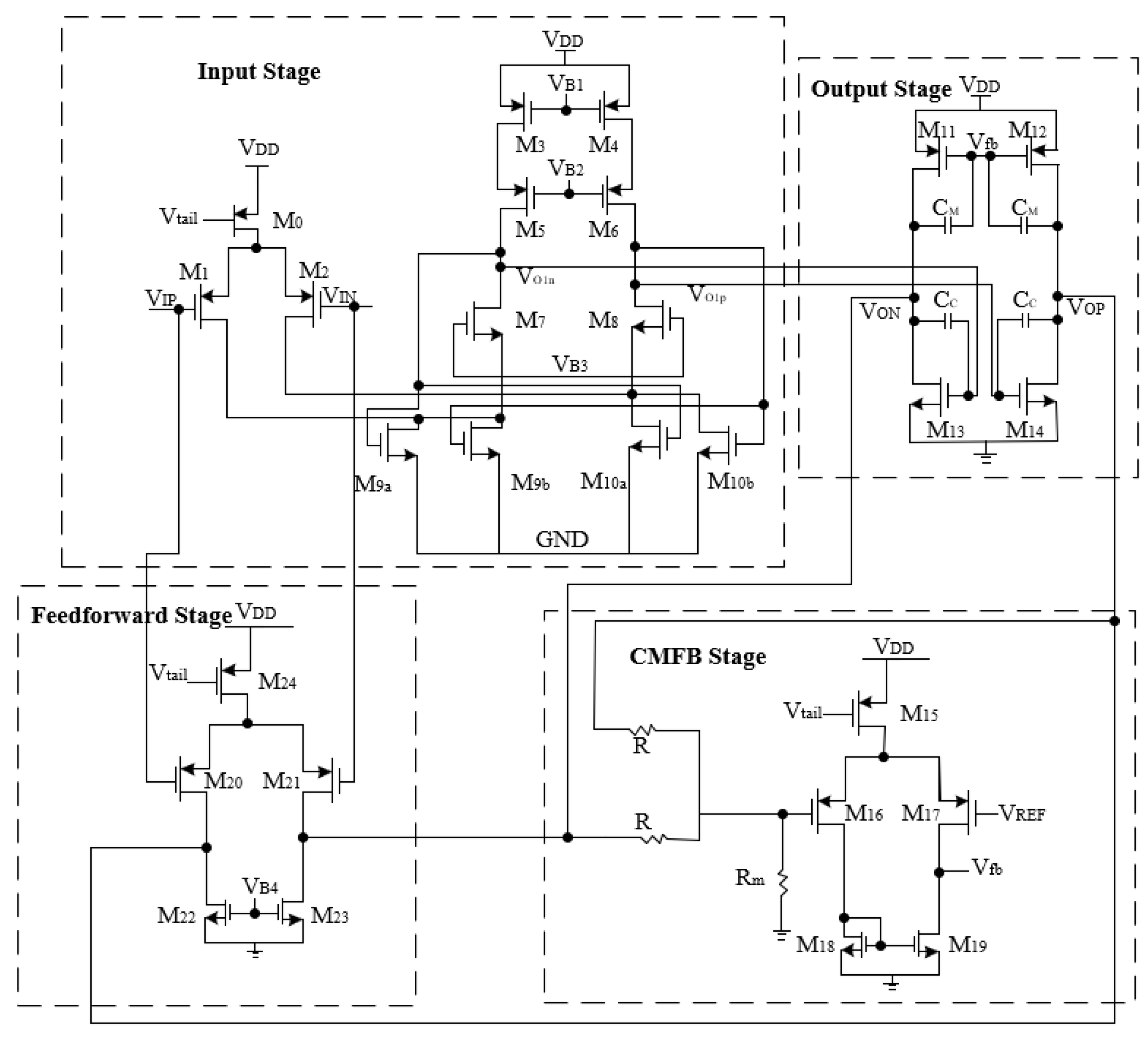
- (a)
- Gain Expression
The transconductance of the input stage, Gm1, is given as:
The voltage gain is expressed as:
- (b) Transfer Function Optimization
As illustrated in Figure 15, the feedforward stage introduces a zero-pole pair in the transfer function, compensating for the dominant pole. This minimizes phase lag and extends the high-frequency bandwidth. The transfer function is given by
Where:
- (c) PSRR
We calculate the PSRR using the method presented in Chapter II. Referring to Figure 10. in Chapter II, the first stage of op amps can be equivalent to , Where:
Referring to the calculation in Figure 9., replace the original b with here and replace with the transfer function of PSRR that can be obtained directly
Assuming ,,,,
If ,,:
Constrained by the above formula, we can easily find the size of each transistor. Table 1 shows the design specifications of this circuit.
And after simulation, we hope to further optimize the performance of PSRR. Compared with the traditional analysis of PSR in the industrial method, we know more intuitively that we can enhance the performance of PSRR by increasing gm or reducing cc according to (64). The simulation results before and after the modification are shown below:
Figure 17.
PSR simulation experiment.
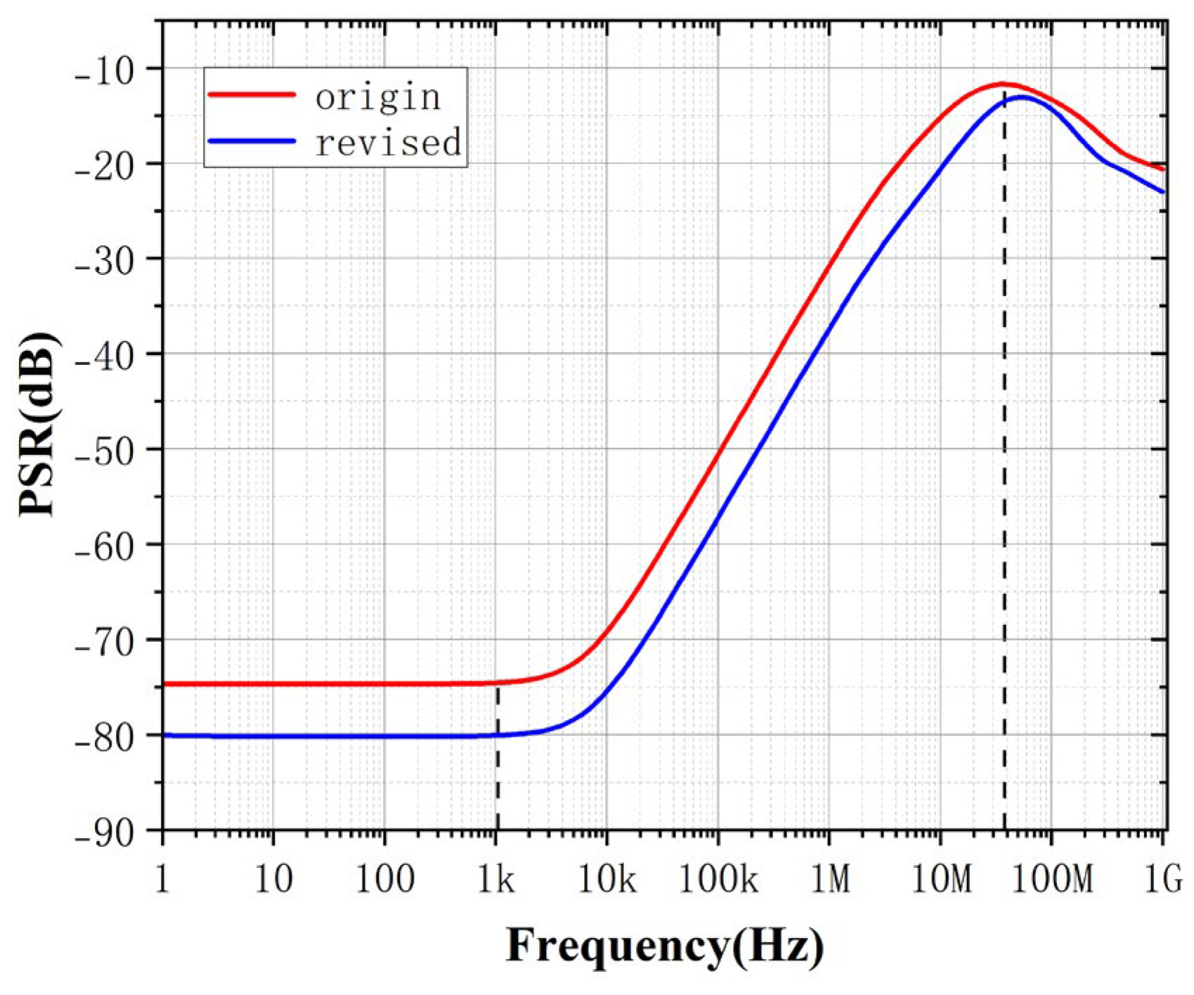
Figure 18.
PSRR simulation experiment.
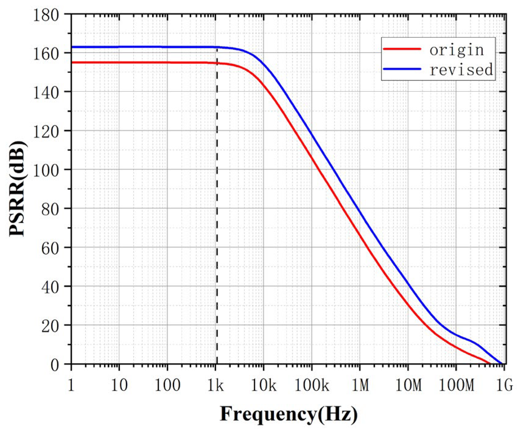
As shown in the above, the modified circuit has improved DC gain performance due to the increase in the width of the input transistor. In addition, the performance of PSR and PSRR is even better, which verifies the ability of PGB to help analog circuit designers improve PSRR more intuitively in complex circuits.
We also performed some other simulations on the circuit. Figure 19 shows the basic indicators of the circuit at different process corners, and Figure 19-d shows the PSRR of the circuit at each process corner after PGB operation adjustment
The PSRR of this circuit is more than 100dB at 100kHz for all process conners. It is also very good at high frequencies. We also did a Monte Carlo simulation, and the results are shown in the Figure 20.
Table 2 shows the simulation results of this circuit and the comparison with other high PSRR op amps. Table 3 shows the comparison between the expected performance and simulation results of the circuit designed using our proposed PSRR calculation method. The design requirements are achieved in all indicators and a good FOM value is achieved. The PSRR calculation method proposed in this article provides a new idea for future circuit design, and the PGB optimization method can also simplify the complex process of PSR calculation.
4. Conclusions
Experimental validation in Section III demonstrates that by leveraging Thevenin’s equivalence principle, the proposed method transforms multi-stage op-amps into simplified black-box models, significantly reducing computational complexity while enhancing intuitive analysis. The introduced PGB metric, which correlates the DC PSRR value with the first dominant pole frequency, eliminates the reliance on exhaustive S-parameter modeling. This enables a computationally efficient evaluation of PSRR performance within the target frequency band. While the PGB framework assumes validity primarily below the GBW—a constraint inherent to its first-order approximation—it remains highly practical for industrial design scenarios where critical PSRR specifications typically reside in low-to-mid frequency ranges. the PGB metric provides actionable insights for optimizing PSRR through parameter adjustments and facilitates rapid comparative analysis of competing circuit topologies.
The proposed framework not only simplifies PSRR analysis for asymmetric and multi-stage circuits but also provides actionable insights for optimizing key parameters (e.g., transconductance, compensation capacitance) to meet stringent industrial requirements. Future work will extend this approach to mixed-signal systems and explore its integration with machine learning-driven design automation tools.
Author Contributions
Conceptualization, Yi Zhang.; methodology, Yi Zhang; software, Yi Zhang; validation, Yi Zhang; formal analysis, Yi Zhang and Ruonan Lin; investigation, Xin Yang and Ruonan Lin; resources, Tailai Li; data curation, Yi Zhang.; writing—original draft preparation, Xin Yang; writing—review and editing, Tailai Li; visualization, Yi Zhang and Xin Yang; supervision, Yi Zhang; project administration, Yi Zhang; All authors have read and agreed to the published version of the manuscript.”
Funding
This research received no external funding.
Data Availability Statement
All data for this article are available
Acknowledgments
None.
Conflicts of Interest
The authors declare no conflicts of interest.
References
- J. S. Kim, S. Ha, H. Jeong and J. Roh, "A High-PSRR NMOS LDO Regulator With Intrinsic Gain-Tracking Ripple Cancellation Technique," in IEEE Transactions on Circuits and Systems I: Regular Papers, vol. 71, no. 11, pp. 4951-4960, Nov. 2024. [CrossRef]
- I. Colli-Menchi, J. Torres and E. Sánchez-Sinencio, "A Feed-Forward Power-Supply Noise Cancellation Technique for Single-Ended Class-D Audio Amplifiers," in IEEE Journal of Solid-State Circuits, vol. 49, no. 3, pp. 718-728, March 2014. [CrossRef]
- C-C. Chiu et al., "A 0.6 V Resistance-Locked Loop Embedded Digital Low Dropout Regulator in 40 nm CMOS With 80.5% Power Supply Rejection Improvement," in IEEE Transactions on Circuits and Systems I: Regular Papers, vol. 62, no. 1, pp. 59-69, Jan. 2015. [CrossRef]
- Y. Choi, W. Tak, Y. Yoon, J. Roh, S. Kwon and J. Koh, "A 0.018% THD+N, 88-dB PSRR PWM Class-D Amplifier for Direct Battery Hookup," in IEEE Journal of Solid-State Circuits, vol. 47, no. 2, pp. 454-463, Feb. 2012. [CrossRef]
- K. A. I. Halonen, W. M. C. Sansen and M. Steyaert, "A micropower fourth-order elliptical switched-capacitor low-pass filter," in IEEE Journal of Solid-State Circuits, vol. 22, no. 2, pp. 164-173, April 1987. [CrossRef]
- Razavi, "Design of Analog CMOS Integrated Circuits," 2nd ed., Xi'an Jiaotong University Press, 2009, pp. 358–400.
- P. E. Allen, D. R. Holberg, "CMOS Analog Circuit Design," 2nd ed., Beijing: Publishing House of Electronics Industry, 2005, pp. 232–234.
- P. R. Gray, P. J. Hurst, S. H. Lewis, and R. G. Meyer, Analysis and Design of Analog Integrated Circuits, 4th ed., Beijing: Higher Education Press, 2005, pp. 410–415.
- Bhar S, Mondal A, Srimani S, et al. A low power driver amplifier for Fully Differential ADC[C]//2019 2nd International Symposium on Devices, Circuits and Systems (ISDCS). IEEE, 2019: 1-6. [CrossRef]
- Yang and T. Lehmann, ‘‘High gain operational amplifiers in 22 nm CMOS,’’ in Proc. IEEE Int. Symp. Circuits Syst. (ISCAS), May 2019, pp. 1–5. [CrossRef]
- S. Chakraborty, A. Pandey, and V. Nath, ‘‘Ultra high gain CMOS op-amp design using self-cascoding and positive feedback,’’ Microsyst. Technol., vol. 23, no. 3, pp. 541–552, Mar. 2017. [CrossRef]
- Yongzhen Chen, Chixiao Chen, Qiang Zhang, Fan Ye and Junyan Ren, ”A 12-bit 200-MS/s sample-and-hold amplifier with a hybrid Miller-Feedforward compensation technique,” 2013 IEEE 10th International Conference on ASIC, 2013, pp. 1-4. [CrossRef]
Figure 3.
Two-stage op-amp circuit after “black-box” abstraction.
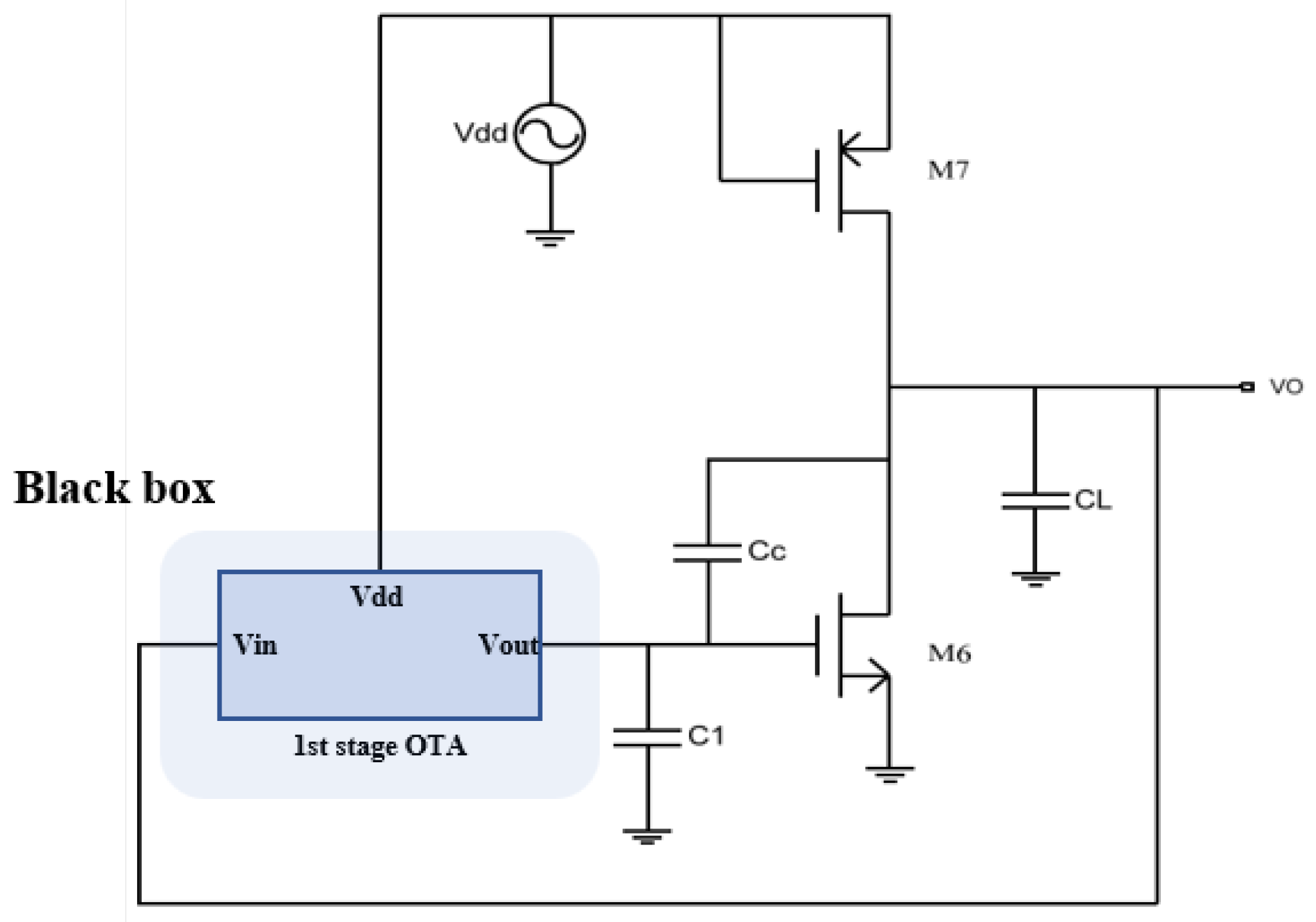
Figure 6.
Thevenin equivalent circuit of the op-amp.
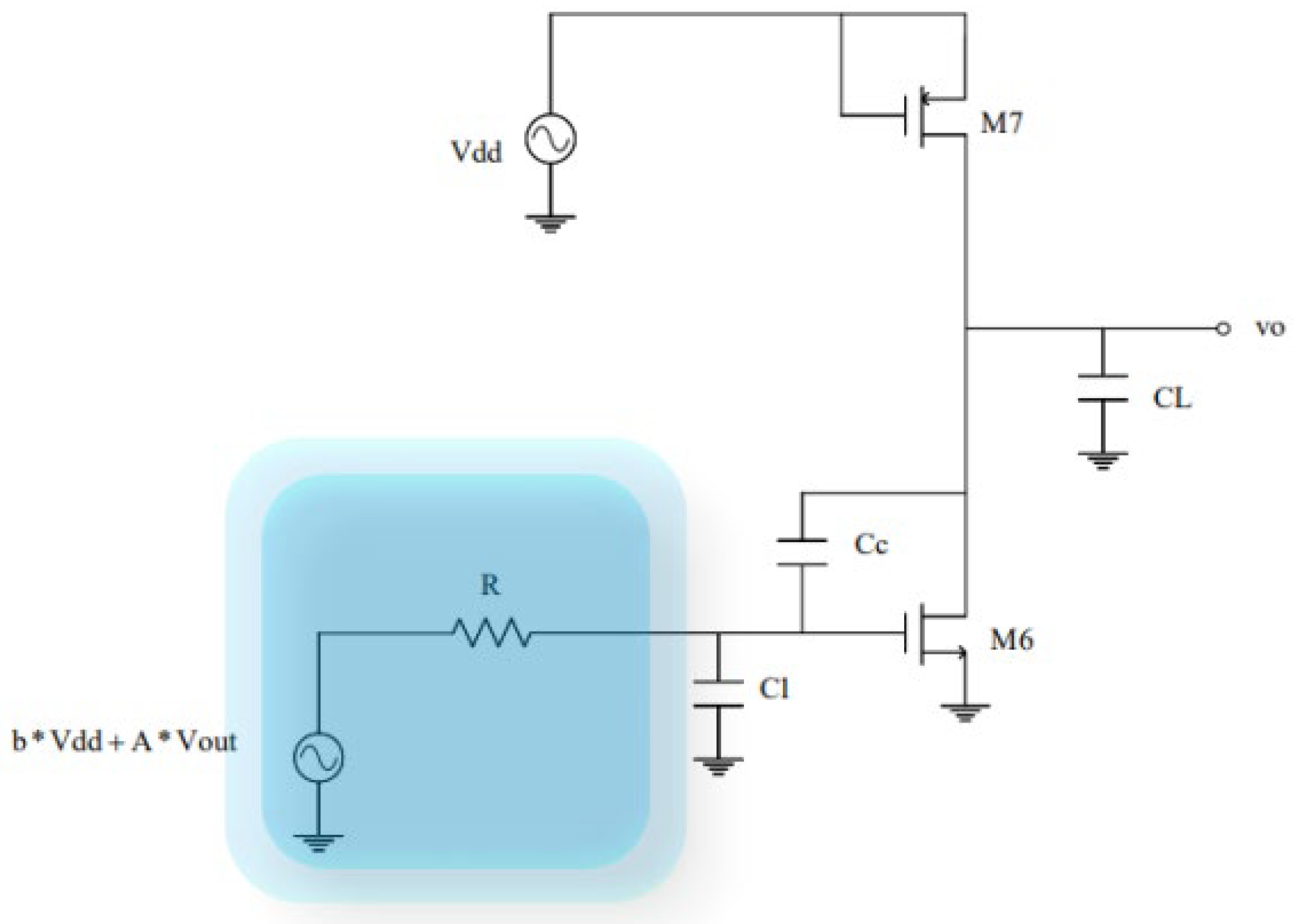
Figure 7.
Small-signal equivalent model.
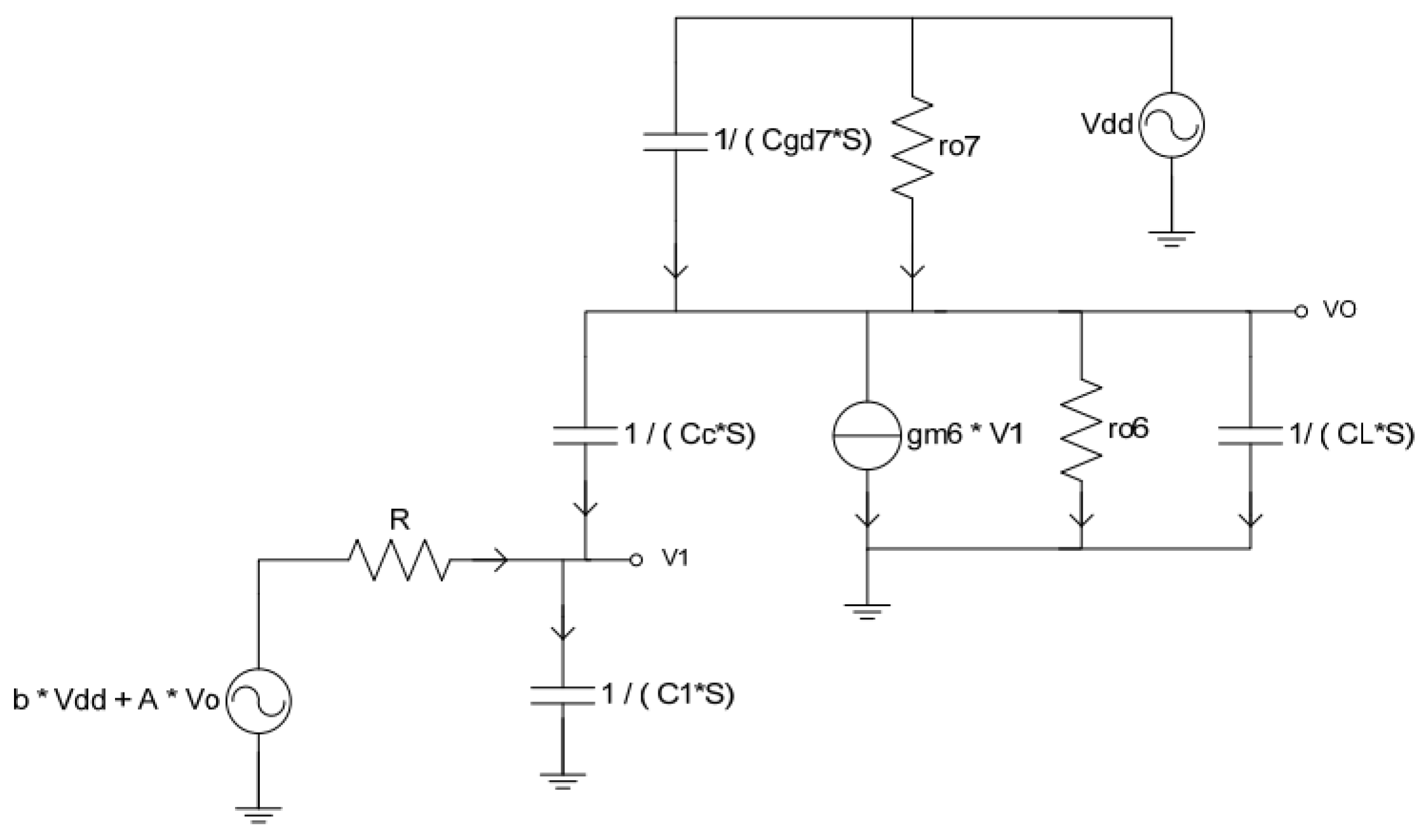
Figure 8.
Impact of varying on the frequency characteristics of PSRR.
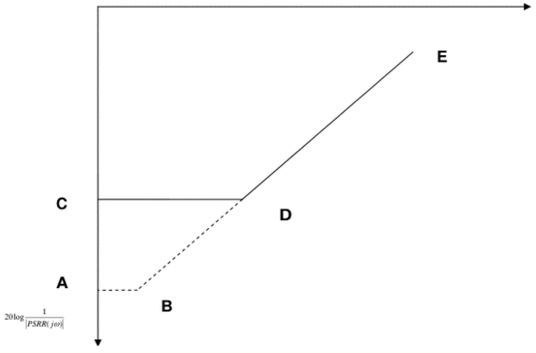
Figure 9.
Simplified flow chart of a common N-input two-stage op amp.
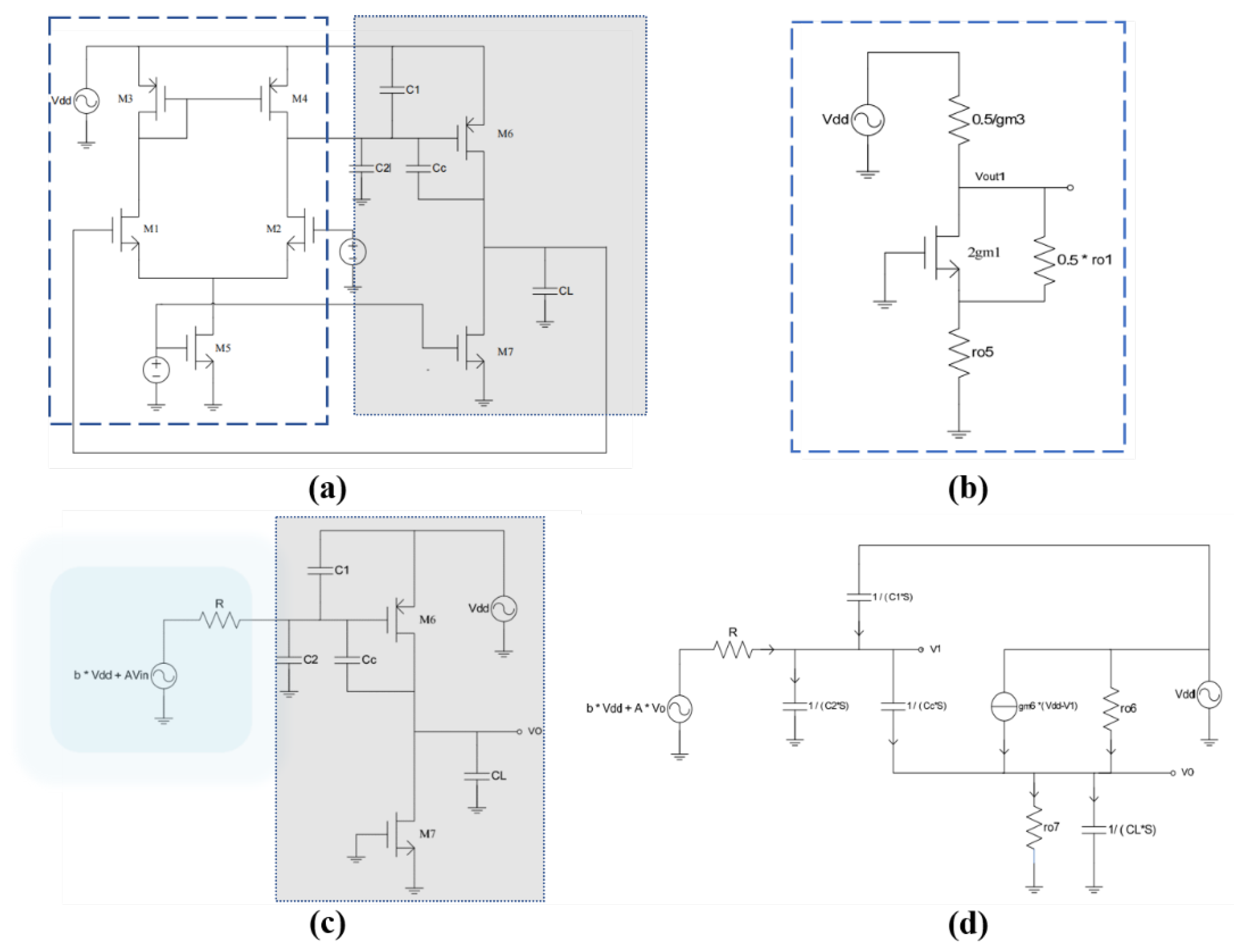
Figure 12.
Folded cascode op-amp simplified using the superposition theorem.
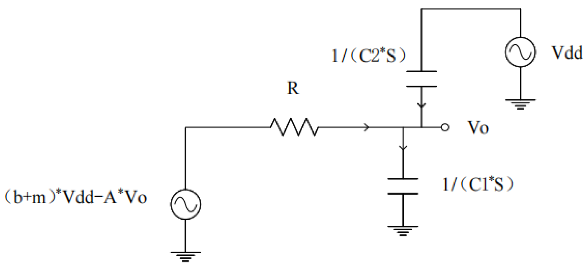
Figure 13.
Simplified flowchart for a typical N-input two-stage op-amp.
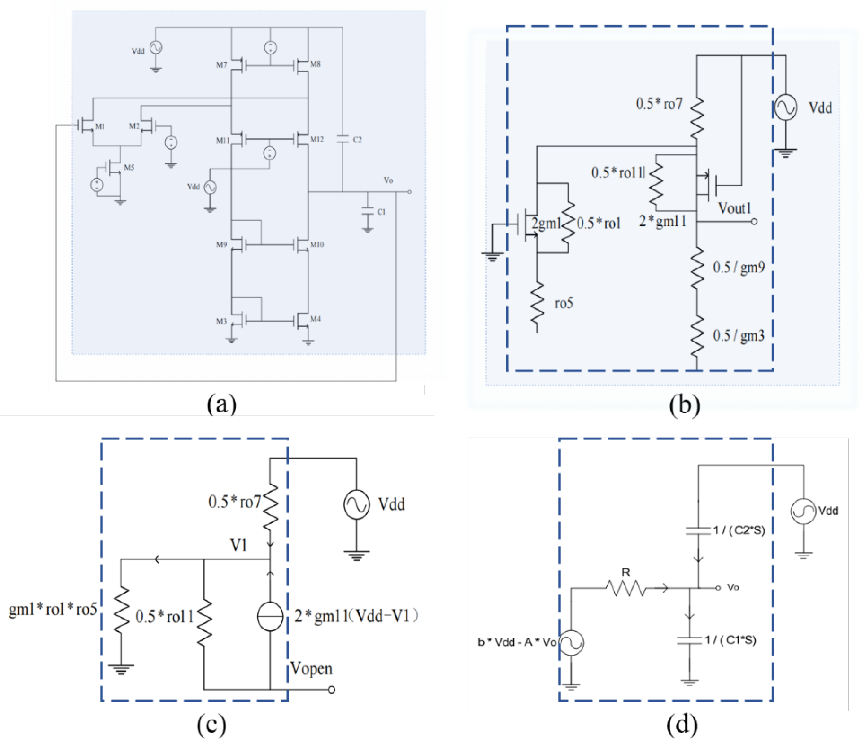
Figure 15.
Equivalent block diagram.
Figure 16.
Gain simulation experiment.
Figure 19.
Simulation results at different process conners of the proposed OTA (a) The AC Gain (b) Phase (c)CMRR (d) PSRR.
Figure 19.
Simulation results at different process conners of the proposed OTA (a) The AC Gain (b) Phase (c)CMRR (d) PSRR.
Figure 20.
Monte Carlo simulation of (a) PSRR (b) Unity gain bandwidth (c) Phase margin (d) Slew Rate (e) CMRR (f) RMS noise.
Figure 20.
Monte Carlo simulation of (a) PSRR (b) Unity gain bandwidth (c) Phase margin (d) Slew Rate (e) CMRR (f) RMS noise.

Table 1.
The design specifications of this circuit.
| Parameters | |
| Supply Volatge(V) | 1.8V |
| Process | 180nm |
| Gain(dB) | >80dB |
| Phase Margin(deg) | >55 |
| GBW(MHz) | >100 |
| SR(V/us) | >80 |
| Power(mW) | <1 |
| CMRR(dB) | - |
| PSRR(dB) | >100 |
| CL(F) | 2p |
| FOM* | - |
Table 2.
Performance of the implemented OTA in comparison to the existing works.
| Parameters | Designed | This Work | 8 | 9 | 10 | 11 |
| Supply Voltage (V) | 1.8V | 1.8V | 1.8V | 1.8V | 2V | 1.2V |
| Process | 180nm | 180nm | 180nm | 180nm | 45nm | 65nm |
| Gain (dB) | >80dB | 83dB | 67dB | 66dB | 141 | 90.17 |
| Phase Margin (deg) | >55 | 61.4 | 54 | 58.5 | 60 | 88.84 |
| GBW (MHz) | <100 | 111.1 | 111.8 | 60 | 101 | 1410 |
| SR (V/us) | >80 | 100 | 32.30 | 95 | 57.7 | - |
| Power (mW) | <1 | 0.95 | 1.37 | 0.55 | 1.2 | 47.25 |
| CMRR (dB) | - | 252 | 127 | 136 | - | |
| PSRR (dB) | >100 | 131 | 68 | 83.2 | 57/67 | - |
| CL (F) | 2p | 2p | 2p | 2.3p | 1p | 4p |
| FOM* | - | 233.8 | 163.2 | 240 | 80 | 119.3 |
Table 3.
Sizes obtained from the multiple constraints.
| Components | W/L(um) |
| M0 | 9.9/1 |
| M1 M2 | 123/1 |
| M3 M4 | 32/3 |
| M5 M6 | 15/1 |
| M7 M8 | 10/0.6 |
| M9a M9b M10a M10b | 2.05/0.945 |
| M11 M12 | 30/1 |
| M13 M14 | 4.9/3.5 |
| M15 | 10/1 |
| M16 M17 M20 M21 | 6/0.18 |
| M18 M19 | 1/1 |
| M22 M23 | 1/4 |
| M25 | 12/1 |
Disclaimer/Publisher’s Note: The statements, opinions and data contained in all publications are solely those of the individual author(s) and contributor(s) and not of MDPI and/or the editor(s). MDPI and/or the editor(s) disclaim responsibility for any injury to people or property resulting from any ideas, methods, instructions or products referred to in the content. |
© 2025 by the authors. Licensee MDPI, Basel, Switzerland. This article is an open access article distributed under the terms and conditions of the Creative Commons Attribution (CC BY) license (http://creativecommons.org/licenses/by/4.0/).
Copyright: This open access article is published under a Creative Commons CC BY 4.0 license, which permit the free download, distribution, and reuse, provided that the author and preprint are cited in any reuse.


