
Submitted:
27 February 2025
Posted:
28 February 2025
You are already at the latest version
Abstract
An ultrathin film capable of exhibiting material properties across and around two different dimensions by bridging two-dimensionality frameworks, called transdimensional (TD) material, offers an exceptional tool to tune various electronic and opto-plasmonic properties of a system that are unattainable from either dimension. Taking an example of the planner periodic arrangement of single-walled carbon nanotube (SWCNT) TD films, we semi-analytically calculate their dynamical conductivities and dielectric responses as a function of the incident photon frequency and SWCNT’s radius using many particles green’s function formalism in Matsubara frequency technique. The periodic array of SWCNTs has an anisotropic dielectric response, which is almost a constant and the same as that of the host dielectric medium in the perpendicular direction of the alignment of the SWCNT array due to the depolarization effect that SWCNTs have. However, the dielectric response depends on the incident photon energy in addition to the film’s thickness, the SWCNT’s sparseness, inhomogeneity, and the SWCNT’s diameter. The energy difference between the resonant absorption peak and the plasmonic peak varies with the thickness of the film. Varying the length of the CNTs, we also observed that the exciton-plasmon coupling strength increases with the increase in length of the SWCNTs. The metallic SWCNT-containing films have comparatively pronounced plasmon resonance peaks at low photon energy than semiconducting SWCNT-containing films. Both metallic and semiconducting SWCNT consisting films have negative refraction for a wide range of energy, making them good candidates for metamaterials.
Keywords:
Single-walled carbon nanotube
; Dielectric response
; Metamaterials
; Exciton-plasmon coupling
; Plasmonics
; Trans-dimensional material
1. Introduction
Since the first observation of a carbon nanotube (CNT) of 50 nanometers diameter in 1952 [1], many scientific studies of synthesis, characterization, and detailed investigation on mechanical, thermal, electronic, optical, and plasmonic properties have been done in carbon nanotubes. In 1975, Oberlin et al. observed a multi-walled CNT (MWCNT) as a hollow tube of rolled graphite in carbon fiber synthesis utilizing the chemical vapor deposition method decomposing benzene and hydrogen at high temperatures in the presence of a transition metal as a catalyst [2]. Dresselhaus et al. contributed to the theoretical investigation of carbon-based materials, namely, carbon whiskers and graphite intercalation compounds, in the late 1970s. [3,4]. The first evidence of CNT production as fiber in carbon anode in arc discharge technique was presented at the Biennial Conference of Carbon in 1978 [5]. MWCNTs were perceived as rolled graphene layers in a cylindrical geometry after Nesterenko et al.’s work on thermoanalytical disproportionation of carbon monoxide to characterize carbon nanoparticles [6]. Howard Tennent received a US patent in producing cylindrical discrete carbon fibrils of diameter in the range of 3.5 to 70 nm [7]. The experimental discovery of MWCNTs by S. Iijima in arc-burned graphite rods and their imaging through a high-resolution electron beam technique of transmission electron microscopy is considered a turning point of CNT research [8]. Within two years after such discovery, it was observed that some single-walled CNTs (SWCNTs) show exceptional conducting behavior [9,10]. Since then, CNTs have received significant attention among researchers in this field because of their high tensile strength (∼ order of Pa for SWCNTs [11]), higher electrical and thermal conductivities, opto-plasmonic properties, and chirality-dependent metallicity.
The plasmon spectrum of SWCNTs is rich in plasmon resonance peaks. Semiconducting SWCNTs have plasmon modes in the visible and ultraviolet (UV) ranges of a few hundred to thousands of terahertz (THz), while metallic SWCNTs have plasmon modes and comparatively intense plasmon peaks in the low-frequency range of only a few THz besides the other plasmon modes in the visible and UV ranges, like semiconducting SWCNTs [12,13]. For a thin film of CNTs, the film’s plasmonic behavior on it’s interaction with light results due to the collective excitons, which can be tuned by changing the radius, sparseness of CNTs, thickness of dielectric medium in which CNTs are immersed, and chirality of the SWCNTs [14,15,16,17]. Note that the permitivity of the host medium is comparatively larger than the permittivities of substrate and superstate, and chirality of the CNTs [14,15,16,17]. Plasmonic interconnect circuits built from CNTs offer a new material platform for nanoscale electronic devices integrated with optoelectronic components as they offer high electrical conductivity, ballistic transportation, resistance to electromigration, and broadband response [20]. Binding a target molecules to the CNT’s surface, CNTs can be used for gas sensing, chemical sensing, and bio-sensing as plasmonic properties of CNT become sensitive in the presence of target molecules [21,22]. SWCNT films’ optical transparency, excellent flexibility, and remarkable potency under mechanical stress make them good candidates for transparent conductive films for liquid crystal display and organic light-emitting diode displays, transparent electrodes in photovoltaic cells, and quantum dots light-emitting diodes [26,27]. The films can also be used in optical modulators and optoelectronic sensors. SWCNT films can be integrated into metamaterials for sub-wavelength imaging in super lenses, cloaking devices, beam-steering technologies, and electromagnetic interference shielding for aerospace and telecommunications [28]. Hybrid plasmonic-CNT structures obtained by incorporating one-dimensional (1D) CNT tubules with other 2D plasmonic materials such as MXenes and graphene are useful for fine-tuning various electrical, optical, thermal, and plasmonic properties as MXenes and graphene provides additional pathways for electron transport and enhances the coupling between MXenes’ or graphene’s localized surface plasmons and the electron-rich CNTs network, amplifying the plasmonic response [23,24,25].
Any SWCNT of chiral indices can be thought of as being a hollow cylinder prepared by rolling a graphene sheet along the specific chiral vector given by , where and represent the graphene lattice vectors. and serve as translation vectors. A scheme of rolling a graphene sheet to obtain different types of SWCNTs is presented in Figure 1. The radius and chiral angle of any SWCNT can be calculated as [29,30,31]
and
where Å is the carbon-to-carbon distance in a graphene sheet. The chiral angle satisfies . equals for a zigzag SWCNT with chiral indices and for an armchair SWCNT with chiral indices . The chiral angle satisfies for chiral SWCNTs. All the armchair SWCNTs are metallic. However, the zigzag SWCNTs are metallic or small band-gap semiconductors based on whether the chiral index n is divisible by 3 or not, respectively. The chiral SWCNTs, whose chiral indices n and m are neither identical nor either one is zero, are quasi-metallic if the chiral indices difference is divisible by 3 and semi-conductive otherwise. Statistically, 1/3rd of SWCNTs are metallic, while the remaining 2/3rd are semiconducting with a small bandgap. Depending on the technological requirement, one can synthesize SWCNTs of specific chirality.
Literature is rich in the study of mechanical, electronic, optical, and plasmonic behavior of a single SWCNTs [32,33,34,35,36]. This paper extends our work to the thin and ultrathin films of homogeneous SWCNTs, which are oriented along the y-axis in periodic alignment. A schematic diagram of the theoretical model considered in this study is presented in Figure 2. Each SWCNT presented in the figure is plotted using Nanotube Modeler Software [37,38], which is a program to generate -coordinates and plot interactive graphics for capped and uncapped nanotubes and nanocones for chosen chirality, tube length, and bond length. The SWCNT-array is immersed in a dielectric medium of thickness d and constant effective relative permittivity . The substrate and superstate have relative permitivities of and , which are relatively much smaller in value than . Each SWCNT has a radius R and length L. The center-to-center distance inter-tube distance satisfies with the minimum ideal distance being the sum of the radii of the two closest tubes. determines the disperseness of SWCNTs in the film with larger signifying highly dispersed SWCNT film. denotes the SWCNT film width. The SWCNTs have uniform electronic charge distribution throughout the surface of the tube.
Taking rings in SWCNT at position vector and SWCNT at , the distance between the rings can be expressed as . For a thin film with a thickness smaller than the distance between rings denoting unit cells of different SWCNTs as shown in Figure 2 i.e., , the electrostatic (Coulomb) interaction between the rings of unit cells becomes so strong that it loses the dependency on its vertical component. As a result, the effective dimensionality of the SWCNT film decreases by one, making it a 2D problem retaining the vertical size, i.e., thickness, as a parameter [16,17]. Such a system with a relatively small thickness, better known as trans-dimensional material (TDM), offers an exceptional tool to tune various opto-plasmonic properties that are unattainable from both 3D bulk and/or single-layered 2D counterparts.
To understand and utilize light-matter interactions in SWCNT and its film at the nanoscale, evaluating and analyzing their dielectric response tensors is crucial as dielectric response functions delineate collective oscillations of free electrons, excitons, and plasmons. The dielectric properties dependent surface plasmons and localized surface plasmon resonances occur on the film’s surface, creating strong electromagnetic fields when free electrons resonate with incident photon [18,19]. We derive a closed-form of mathematical expressions for the dynamical (as a function of photon frequency) dielectric response functions of the SWCNT array as presented in Figure 2 using the many-particle Green’s function technique exploiting Matsubara frequency approach as discussed in Ref. [39].
We organize this paper as follows. We orient ourselves with a mathematical overview for dielectric responses for SWCNTs in Sec. Section 2. We first evaluate a SWCNT’s dynamic conductivity, which is then used to evaluate its polarizability and dielectric response functions. A comparative study of the dynamical conductivity of two different types of SWCNTs is presented, followed by the dynamical permittivities and dynamical conductivity of a SWCNT used in the SWCNT array. The dielectric response functions of an array of identical SWCNTs are presented in Sec. Section 3. Therein, we set up the Hamiltonian of the system, determine the interaction Hamiltonian for the SWCNT film, and present the closed-form of expressions for dielectric responses. Taking (11,0) SWCNT film as a reference, we discuss our research findings in Sec. Section 4. We present conclusions in Sec. Section 5. We have used Gaussian units throughout this paper unless otherwise stated.
2. Dielectric Responses of an Isolated SWCNT
When light interacts with a valence electron of carbon in a SWCNT, the electron gets excited to the conduction band, leaving a hole behind, thereby creating an electron-hole pair called exciton and inducing an anisotropic polarization. The induced polarization is dominant along the SWCNT axis and negligible in the directions perpendicular to the SWCNT alignment due to the weakening of the response to incident photon along the width of the tube called transverse depolarization effect [40,41]. The photon frequency and SWCNT radius-dependent axial polarizability of an SWCNT can be expressed in terms of its axial surface conductivity as [42]
where is an infinitesimal frequency parameter. The dynamical conductivity of a SWCNT is estimated using the well-known method of band structure calculations [41,43]. The conducting behavior of SWCNTs significantly varies with chirality and divisibility of the difference between chiral indices by 3. For example, (9,0) SWCNT is metallic, while (10,0) SWCNT is a semiconducting one. The exciton-plasmon spectrum for the conductivity of metallic SWCNT significantly differs from the semiconducting one, as shown in Figure 3.
One may ask how the plasmon spectrum for the conductivity of an isolated SWCNT, measured by , can have such intense resonance peaks. The quantity can be expressed as
where and denote the real and imaginary parts respectively. At the energy value, in which the real part approaches zero, and the imaginary part switches the sign simultaneously, the quantity will have a significantly large value. As can be smaller than unity when the imaginary part becomes zero, the can be larger than unity. The plasmon resonance appears at a lower photon energy than that of the exciton for metallic (9,0) SWCNT. The same is not true for semiconducting (10,0) SWCNT. In the chosen window of the photon energy, i.e.,0.75 − 4.25 eV, (10,0) SWCNT has three intense exciton resonance peaks, while the (9,0) SWCNT has only one resonance peak in this energy range for each real, imaginary and energy-loss parts of the spectrum.
Knowing the conductivity of a single SWCNT, one can easily evaluate its dielectric response functions using
where denotes the surface area of a SWCNT in which the charge is uniformly distributed, and is the number of SWCNTs per unit volume. For an isolated SWCNT, . Consequently, . One can normalize the axial surface conductivity of an SWCNT as
such that is a dimensionless axial surface conductivity as a function of dimensionless energy and an infinitesimal dimensionless energy , where is the carbon atom’s nearest neighbor overlap integral in a SWCNT. Substituting the value of from Eq. (6) to Eq. (5), one gets,
Consequently, we have
for the real and imaginary parts of dielectric response. The loss function , determined from the plasmon spectra, is given by
For an illustrative purpose, the dimensionless response functions, namely, longitudinal conductivities and longitudinal dielectric functions for a (11,0) SWCNT, are presented in Figure 4. gives us the surface plasmon’s density of states, which is nonzero when the imaginary part of vanishes and the real part of also approaches to zero. The quantity is nonzero only if the is zero and approaches to zero at the same time.
3. Dielectric responses of SWCNT Films
From the principle of the second quantization, one can write the Hamiltonian of free exciton on the surface of the SWCNT as
where is an exciton energy in its s-subband. is the electron’s quasimomentum in the plane, where is the quasimomentum component along the SWCNT alignment and is along the perpendicular direaction to the plane. The exciton annihilation and creation operators follow boson statistics and satisfy the following identities:
The complication arises when we have not just a single SWCNT but an array of SWCNTs as they interact via dipole-dipole interaction. The interaction Hamiltonian can written as [17]
where
is the interaction potential with being the transition dipole associated with s-subband excitation. , , a, and are the intraband plasma oscillation frequency, the surface electron density, the lattice translation period, and the Fourier transform of the SWCNTs’ dipole-dipole interaction, respectively. The total Hamiltonian of the system is the sum of Eqs. (10) and (12):
which can be analytically diagonalized using the Bogoliubov-Valatin transformation as presented in Ref [44].
For the SWCNT array, the dielectric response is anisotropic, which along the direction perpendicular to the SWCNT alignment remains constant with the value of the dielectric constant of host medium, while along the SWCNT alignment, it is given as [17]
where is the ratio of the SWCNTs volume to the volume of the host dielectric medium. measures how sparse SWCNTs are in the film. has a lower value for larger intertube distance and satisfies , implying that screening of host dielectric medium always present in SWCNT array even at the very tightly packed SWCNT array. The screening leads to broadening excitonic and plasmonic peaks and enhancing exciton-plasmon coupling. and in Eq. (15) are the zeroth-order modified cylindrical Bessel functions. The dielectric response of the SWCNT array is not only the function of photon energy and SWCNT radius similar to a single SWCNT, but it is also a function of the volumetric fraction , permittivities , , and of substrate, superstrate, and the dielectric medium holding the SWCNT array and quasi-momentum along the SWCNT alignment. Being the ratio of the physical quantities with the same dimensionality, the dielectric response function expressed in Eq. (15) is a dimensionless quantity.
4. Discussion
For , the right side of Eq. (15) equals unity, implying that the dielectric response of the SWCNT array equals the host dielectric medium’s permittivity, which makes the dielectric response function isotropic. For the non-zero value of or , the component of the dielectric response is a complex function. The for two different composite films, one consisting of a periodic array of (9,0) SWCNTs and the other consisting of (10,0) SWCNTs, are presented in Figure 5. The SWCNT layers are embedded in a dielectric medium of thickness and relative permittivity , where R is the radius of the respective film’s SWCNT. The fractional volume of CNT in both these composites is . The real part represents the exciton refraction resonance, the imaginary represents the exciton absorption resonance, and represents the plasmon response. The plasmon mode has a resonance at the point in which changes sign from negative to positive, and approaches to zero. The plasmon response is positive for the entire energy range, indicating that energy loss is unavoidable. Even in the wide range of energy window (up to ∼ 4.0 eV), only one resonance is present for (9,0) SWCNT film. However, one witnesses two resonances for (10,0) SWCNT film for photon energy up to ∼ 2.6 eV. The plasmon resonance appears at a lower energy than the excitonic resonance for (9,0) SWCNT film. The same is not true (10,0) SWCNT film. The plasmon spectrum is comparatively more pronounced in (9,0) than in (10,0) SWCNT film.
The real part of the dielectric response function is negative for a large range of photon energy for both (9,0) and (10,0) SWCNT films, making both SWCNT films good candidates for hyperbolic metamaterials. The energy range, however, depends on the chirality of constituent SWCNTs. The exciton-plasmon spectra of homogenous arrays of any metallic SWCNTs such as (12,0), (15,0), (18,0), etc SWCNTs are expected to behave similarly to (9,0) SWCNT arrays. At the same time, resonance intensity and photon energy for resonances depend on the particular metallic SWCNT that the film consists of. The SWCNT films are made up of semiconducting SWCNT arrays such as (13,0), (16,0), (19,0), etc. SWCNTs have similar behavior to an array of (10,0) SWCNTs. The exciton-plasmon coupling strength is stronger in the SWCNT array than in a single SWCNT. The inhomogeneity effect abruptly increases the exciton-plasmon coupling [15] for a mixture of SWCNTs of slightly different diameters. Comparing the dielectric responses for a single homogeneous array presented in Ref. [14], one can conclude that the dielectric medium contains more than a single array of identical SWCNTs, the intensity of the response function increases.
Substituting the expression of the volume of an isolated SWCNT and the composite volume, can be expressed as , which depends on the thickness of the film and SWCNT sparseness. Choosing a fixed value of , one can observe the effect of film thickness on the exciton-plasmon spectra varying the value of . Note that is smaller for a larger value of d. Figure 6 shows a comparative study of dielectric responses for three different values of .
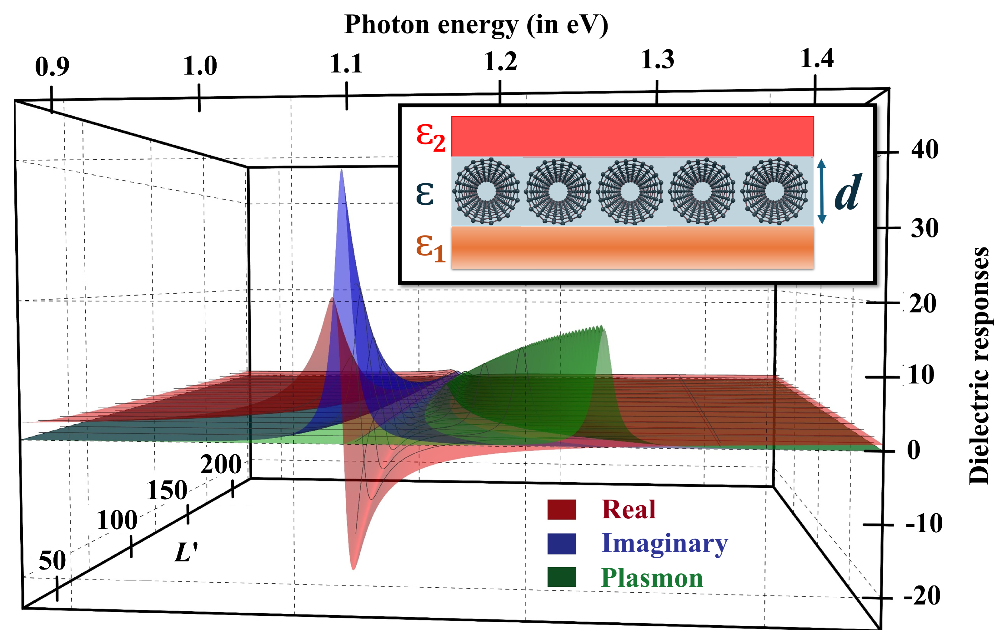
As shown in Eq. (15), the dielectric response function of the SWCNT array is electron quasi-momentum q-dependent. The minimum non-zero value that q can take is , where L is the length of a SWCNT. One can dig a little more into how the length of a SWCNT plays a role in the minimum value of q. For , the longitudinal component of the response functions reads
where is the length of a SWCNT in terms of its circumference. See Figure 7 for the dielectric response function at the minimum nonzero value of momentum .
The major contribution to the dielectric response comes from the momentum. At the same time, one should not forget that with also have a non-zero contribution to the response function, which decays exponentially. The exciton and the plasmon resonances approach each other more closely for than for the larger q. However, the intensity of each of the resonance peaks for is smaller than the large q counterpart. Thus, the resonance intensity and exciton-plasmon coupling strength depend on the SWCNT length. The momentum has a lower value for a longer SWCNT than the shorter one. As the CNT length increases, the plasmon resonance comes closer to the exciton resonance strengthening the exciton-plasmon coupling.
Making use of SWCNTs and their thin films in the current technology is not free from challenges. One of the major challenges using the currently available synthesis methods is producing SWCNTs of a specific chirality and their scalability [45]. Although some claims on producing pure SWCNTs have been reported, some issues, such as removing amorphous carbon, washing out metallic catalysts after catalytic SWCNT synthesis, and yielding defect-free SWCNTs, remain [46]. As chirality control is usually an issue in SWCNT production, having a consistent film thickness, as this article proposed, needs extra work in the experimental setup, which may have not only inhomogeneous mixing of SWCNTs of different chirality but also have tubular misalignment and inter-tube junction resistance due to phonon scattering. The phonon scattering at the inter-tube junction reduces the conductivity of SWCNT film. In future studies, we will focus on the phonon scattering at inter-tube junctions and its effect on dielectric responses in the homogeneous SWCNT arrays and inhomogeneous arrays of SWCNTs of approximately the same diameters. Future work will concentrate on creating hybrid materials combining SWCNTs with other materials, such as graphene and polymers, in search of optoelectronic performance enhancements.
5. Conclusions
Using Green’s functions theory for many-body systems in the Matsubara frequency approach, we derived a closed form of mathematical expression for the dielectric response function of a periodic array of identical SWCNTs embedded in a dielectric medium with comparatively higher permittivities than substrates and superstates. The dielectric response functions of SWCNTs and its array are both anisotropic. The conducting nature of SWCNTs depends on the chirality resulting from turning graphene sheets into tubules. The SWCNT’s photon energy and cylindrical tube’s radius-dependent dynamical conductivity are calculated using the method of the band structure theory. The dielectric response of the SWCNT film along the perpendicular direction of the SWCNT alignment is constant and matches the value of the host dielectric medium, while the same along the direction of SWCNT alignment takes a complex function, which depends on various parameters, namely, photon energy, the radius of SWCNT, volumetric fraction of SWCNT , relative permittivity of the host medium of high dielectric constant, and substrate and superstrate of low permitivities and dynamic conductivity of each SWCNT in the film. The expression we derived for SWCNT film’s dielectric response functions links the SWCNT film dielectric responses to the individual SWCNT’s conductivity and the individual SWCNT’s plasma frequency. The screening of the host dielectric medium is inevitable in an SWCNT array primarily because of its geometry.
The excitonic and plasmonic peaks come closer in the periodic array of SWCNTs than in a SWCNT, increasing the exciton-plasmon coupling. The real part of the dielectric response function is negative for a vast range of photon energy in both cases of having an array of metallic and semiconducting SWCNTs, making them good candidates for hyperbolic metamaterials. The finding is consistent with a recent experimental observation of the hyperbolic metamaterial behavior for horizontally aligned films of SWCNTs presented in Ref. [47]. We revealed that the exciton-plasmon resonance peaks are closest to the minimum nonzero value of q, and the resonance intensity and exciton-plasmon coupling strength depend on the SWCNTs’ length.
Funding
This research was funded by the 2024 Ralph E. Powe Junior Faculty Enhancement Awards, provided by Oak Ridge Associated Universities (ORAU).
Data Availability Statement
Data obtained in this research is included in the paper. Any raw data will be available requesting the author.
Acknowledgments
The author gratefully acknowledges the support of the 2024 Ralph E. Powe Junior Faculty Enhancement Awards, provided by Oak Ridge Associated Universities (ORAU).
Conflicts of Interest
The author declares no conflicts of interest.
Abbreviations
The following abbreviations are used in this manuscript:
| CNT | Carbon nanotube |
| SWCNT | Single-Walled carbon nanotube |
| MWCNT | Multi-Walled carbon nanotube |
| THz | Terahertz |
| 1D | one-dimensional |
| 2D | two-dimensional |
| 3D | three-dimensional |
| TD | trans-dimensional |
| UV | ultraviolet |
| TDM | trans-dimensional material |
| ORAU | Oak Ridge Associated Universities |
References
- Radushkevich, L.V.; Lukyanovich, V.M. On the structure of carbon produced at thermal decomposition of carbon monoxide on an ironcontact. Journal of Physical Chemistry 1952, 26, 88–95. [Google Scholar]
- Oberlin, A.; Endo, M.; Koyama, T. Filamentous growth of carbon through benzene decomposition. Journal of Crystal Growth 1976, 32, 335–349. [Google Scholar] [CrossRef]
- Dresselhaus, M.S.; Dresselhaus, G.; Eklund, P.C.; Chung, D.D.L. Lattice vibrations in graphite and intercalation compounds of graphite, Materials Science and Engineering 1977, 31, 141–152. [CrossRef]
- Dresselhaus, M.S.; Dresselhaus, G.; Fischer, J.E. Graphite intercalation compounds: Electronic properties in the dilute limit. Phys. Rev. B 1977, 15, 3180. [Google Scholar] [CrossRef]
- Abrahamson, J.; Wiles, P. G.; Rhoades, B. L. Structure of carbon fibres found on carbon arc anodes. Carbon 1999, 37, 1873–1874. [Google Scholar] [CrossRef]
- Nesterenko, A. M.; Kolesnik, N. F.; Akhmatov, Y. S.; Suhomlin, V I; Prilutskii, O. V. Osobennosti fazovogo sostava i struktury produktov vzaimodeistviya NiO i Fe2O3 s okis’yu ugleroda. Izvestia Akademii Nauk SSSR, Seriya Metally 1982, 3, 12–17. [Google Scholar]
- Tennent, H.G. Carbon fibrils, method for producing same and compositions containing same. US Patent # 4663230, issued 1987-05-05.
- Iijima, S. Helical microtubules of graphitic carbon. Nature 1991, 354, 56–58. [Google Scholar] [CrossRef]
- Mintmire, J.W.; Dunlap, B.I.; White, C.T. Are fullerene tubules metallic? Physical Review Letters 1992, 68, 631–634. [Google Scholar] [CrossRef]
- Iijima, S.; Ichihashi, T. Single-shell carbon nanotubes of 1-nm diameter. Nature 1993, 363, 603–605. [Google Scholar] [CrossRef]
- Takakura, A.; Beppu, K.; Nishihara, T.; Fukui, A.; Kozeki, T.; Namazu, T.; Miyauchi, Y.; Itami, K. Strength of carbon nanotubes depends on their chemical structures. Nat Commun 2019, 10, 3040. [Google Scholar] [CrossRef]
- Kempa, K. , Chura, R. Plasmons in Carbon Nanotubes. In: Liz-Marzán, L.M., Giersig, M. (eds) Low-Dimensional Systems: Theory, Preparation, and Some Applications. NATO Science Series 2003, 91. Springer, Dordrecht.
- Bondarev, I. V.; Meliksetyan, A. V. Possibility for exciton Bose-Einstein condensation in carbon nanotubes. Phys. Rev. B 2014, 89, 045414. [Google Scholar] [CrossRef]
- Adhikari, C.M.; Bondarev, I.V. Optical response of ultrathin periodically aligned single-wall carbon nanotube films. Mrs Adv. 2020, 5, 2685. [Google Scholar] [CrossRef]
- Adhikari, C.M.; Bondarev, I.V. Controlled exciton–plasmon coupling in a mixture of ultrathin periodically aligned single-wall carbon nanotube arrays. J. Appl. Phys. 2021, 129, 015301. [Google Scholar] [CrossRef]
- Keldysh, L.V. Coulomb interaction in thin semiconductor and semimetal films. Engl. Transl. JETP Lett. 1980, 29, 658. [Google Scholar]
- Bondarev, I.V.; Adhikari, C.M. Collective Excitations and Optical Response of Ultrathin Carbon-Nanotube Films. Phys. Rev. Appl. 2021, 15, 034001. [Google Scholar] [CrossRef]
- Kosuda, K.; Bingham, J.; Wustholz, K.; Van Duyne, R.; Groarke, R. Nanostructures and surface-enhanced Raman Spectroscopy. In Comprehensive Nanoscience and Nanotechnology; Elsevier: Amsterdam, The Netherlands, 2016; 117–152. [Google Scholar]
- Vaghasiya, H.; Miclea, P.-T. Investigating Laser-Induced Periodic Surface Structures (LIPSS) Formation in Silicon and Their Impact on Surface-Enhanced Raman Spectroscopy (SERS). Optics 2023, 4, 538–550. [Google Scholar] [CrossRef]
- Liu,Y. ; Zhang, J.; Liu, H.; Wang, S.; Peng, L.M. Electrically driven monolithic subwavelength plasmonic interconnect circuits. Sci Adv. 2017, 3, e1701456. [Google Scholar] [CrossRef]
- Gupta, B.D.; Pathak, A.; Semwal, V. Carbon-Based Nanomaterials for Plasmonic Sensors: A Review. Sensors (Basel) 2019, 19, 3536. [Google Scholar] [CrossRef]
- Duan, Q.; Liu, Y.; Chang, S.; Chen, H.; Chen, J.-H. Surface Plasmonic Sensors: Sensing Mechanism and Recent Applications. Sensors 2021, 21, 5262. [Google Scholar] [CrossRef] [PubMed]
- Serafinelli, C.; Fantoni, A.; Alegria, E.C.B.A.; Vieira, M. Hybrid Nanocomposites of Plasmonic Metal Nanostructures and 2D Nanomaterials for Improved Colorimetric Detection. Chemosensors 2022, 10, 237. [Google Scholar] [CrossRef]
- Pyo, S.; Eun, Y.; Sim, J.; Kim, K.; Choi, J. Carbon nanotube-graphene hybrids for soft electronics, sensors, and actuators. Micro and Nano Syst Lett 2022, 10, 9. [Google Scholar] [CrossRef]
- Chaudhuri, K.; Alhabeb, M.; Wang, Z.; Shalaev, V.; Gogotsi, Y.; Boltasseva, A. Highly Broadband Absorber Using Plasmonic Titanium Carbide (MXene). ACS Photonics 2018, 5, 10–1021. [Google Scholar] [CrossRef]
- Jiang, K. Chapter 4 - Carbon Nanotubes for Displaying. Editor(s): Huisheng Peng, Qingwen Li, Tao Chen. In Micro and Nano Technologies, Industrial Applications of Carbon Nanotubes. Elsevier, 2017, pp.101-–127. [CrossRef]
- Singh, B.P.; Sikarwar, S.; Pandey, K.K.; Manohar, R.; Depriester, M.; Singh, D.P. Carbon Nanotubes Blended Nematic Liquid Crystal for Display and Electro-Optical Applications. Electron. Mater. 2021, 2, 466–481. [Google Scholar] [CrossRef]
- Zecchi, S.; Cristoforo, G.; Piatti, E.; Torsello, D.; Ghigo, G.; Tagliaferro, A.; Rosso, C.; Bartoli, M. A Concise Review of Recent Advancements in Carbon Nanotubes for Aerospace Applications. Micromachines 2025, 16, 53. [Google Scholar] [CrossRef]
- Obitayo, W.; Liu, T. A Review: Carbon Nanotube-Based Piezoresistive Strain Sensors. Journal of Sensors 2012, 652438. [Google Scholar] [CrossRef]
- Kolahdouz, M.; Xu, B.; Nasiri, A.F.; Fathollahzadeh, M.; Manian, M.; Aghababa, H.; Wu, Y.; Radamson, H.H. Carbon-Related Materials: Graphene and Carbon Nanotubes in Semiconductor Applications and Design. Micromachines 2022, 13, 1257. [Google Scholar] [CrossRef] [PubMed]
- Ando, T. The electronic properties of graphene and carbon nanotubes. NPG Asia Mater 2009, 1, 17–21. [Google Scholar] [CrossRef]
- Nanot, S. , Hároz, E.H., Kim, J.-H., Hauge, R.H. and Kono, J. Optoelectronic Properties of Single-Wall Carbon Nanotubes. Adv. Mater. 2012, 24, 4977–4994. [Google Scholar] [CrossRef]
- Rai, D.P. , Singh, Y.T., Chettri, B. et al. A theoretical investigation of electronic and optical properties of (6,1) single-wall carbon nanotube (SWCNT). Carbon Lett. 2021, 31, 441–448. [Google Scholar] [CrossRef]
- Itas, Y.S.; Suleiman, A.B.; Ndikilar, C.E.; Lawal, A.; Razali, R.; Idowu, I.I.; Khandaker, M.U.; Ahmad, P.; Tamam, N.; Sulieman, A.; et al. Computational Studies of the Excitonic and Optical Properties of Armchair SWCNT and SWBNNT for Optoelectronics Applications. Crystals 2022, 12, 870. [Google Scholar] [CrossRef]
- Preciado-Rivas, M.R.; Torres-Sánchez, V. A.; Mowbray, D. J. Optical absorption and energy loss spectroscopy of single-walled carbon nanotubes, Phys. Rev. B 2019, 100, 235429. [Google Scholar] [CrossRef]
- Nanot, S.; Thompson, N. A.; Kim, J.-H.; Wang, X.; Rice, W.D.; Hároz, E. H.; Ganesan, Y.; Pint C., L.; Kono, J. Single-Walled Carbon Nanotubes. In: Vajtai, R. (eds) Springer Handbook of Nanomaterials. Springer Handbooks. Springer, Berlin, Heidelberg. (2013).
- Melchor, S.; Dobado, J.A. An algorithm for connecting two arbitrary carbon nanotubes, Journal of Chemical Information and Computer Sciences 2004, 44, 1639–1646.
- Johnson, J.E.; Speir, J.A. Quasi-equivalent Viruses: A Paradigm for Protein Assemblies. JMB 1997, 269, 665–675. [Google Scholar] [CrossRef] [PubMed]
- Mahan, G.D. Many-particle physics (Kluwer Academic, New York, 2000), 3rd ed.
- Tasaki, S. i; Maekawa, K.; Yamabe, T. π-band contribution to the optical properties of carbon nanotubes: Effects of chirality. Phys. Rev. B 1998, 57, 9301. [Google Scholar] [CrossRef]
- Ando, T. Theory of Electronic States and Transport in Carbon Nanotubes, J. Phys. Soc. Jpn. 2005, 74, 777. [Google Scholar] [CrossRef]
- Bondarev, I.V.; Woods, L.M.; Tatur, K. Strong exciton-plasmon coupling in semiconducting carbon nanotubes. Phys. Rev. B 2009, 80, 085407. [Google Scholar] [CrossRef]
- Ando, T. Excitons in Carbon Nanotubes, J. Phys. Soc. Jpn. 1997, 66, 1066. [Google Scholar] [CrossRef]
- Adhikari, C.M.; Morris, D.M.; Noonan, T.W.; Neupane, T.; Lamichhane, B.R.; Gautam, B.R. Dispersion in Single-Wall Carbon Nanotube Film: An Application of Bogoliubov–Valatin Transformation for Hamiltonian Diagonalization. Condens. Matter 2023, 8, 53. [Google Scholar] [CrossRef]
- Sakurai, S.; Inaguma, M.; Futaba, D. N.; Yumura, M.; Hata, K. A Fundamental Limitation of Small Diameter Single-Walled Carbon Nanotube Synthesis-A Scaling Rule of the Carbon Nanotube Yield with Catalyst Volume. Materials 2013, 6(7), 2633–2641. [Google Scholar] [CrossRef]
- Daneshvar, F.; Chen, H.; Noh, K.; Sue, H.J. Critical challenges and advances in the carbon nanotube–metal interface for next-generation electronics. Nanoscale Adv. 2021, 3, 942–962. [Google Scholar] [CrossRef]
- Roberts, J.A.; Yu, S.-J.; Ho, P.-H.; Schoeche, S.; Falk, A.L.; Fan, J.A. Tunable Hyperbolic Metamaterials Based on Self-Assembled Carbon Nanotubes, Nano Letters 2019, 19(5), 3131–3137. [CrossRef]
Figure 1.
A schematic diagram showing the rolling direction for the most general chiral with chirality vector and two special cases of achiral, namely, zigzag for and armchair SWCNTs.
Figure 1.
A schematic diagram showing the rolling direction for the most general chiral with chirality vector and two special cases of achiral, namely, zigzag for and armchair SWCNTs.

Figure 2.
A schematic diagram showing a planner periodic array of identical non-chiral SWCNTs taken in our theoretical model.
Figure 2.
A schematic diagram showing a planner periodic array of identical non-chiral SWCNTs taken in our theoretical model.
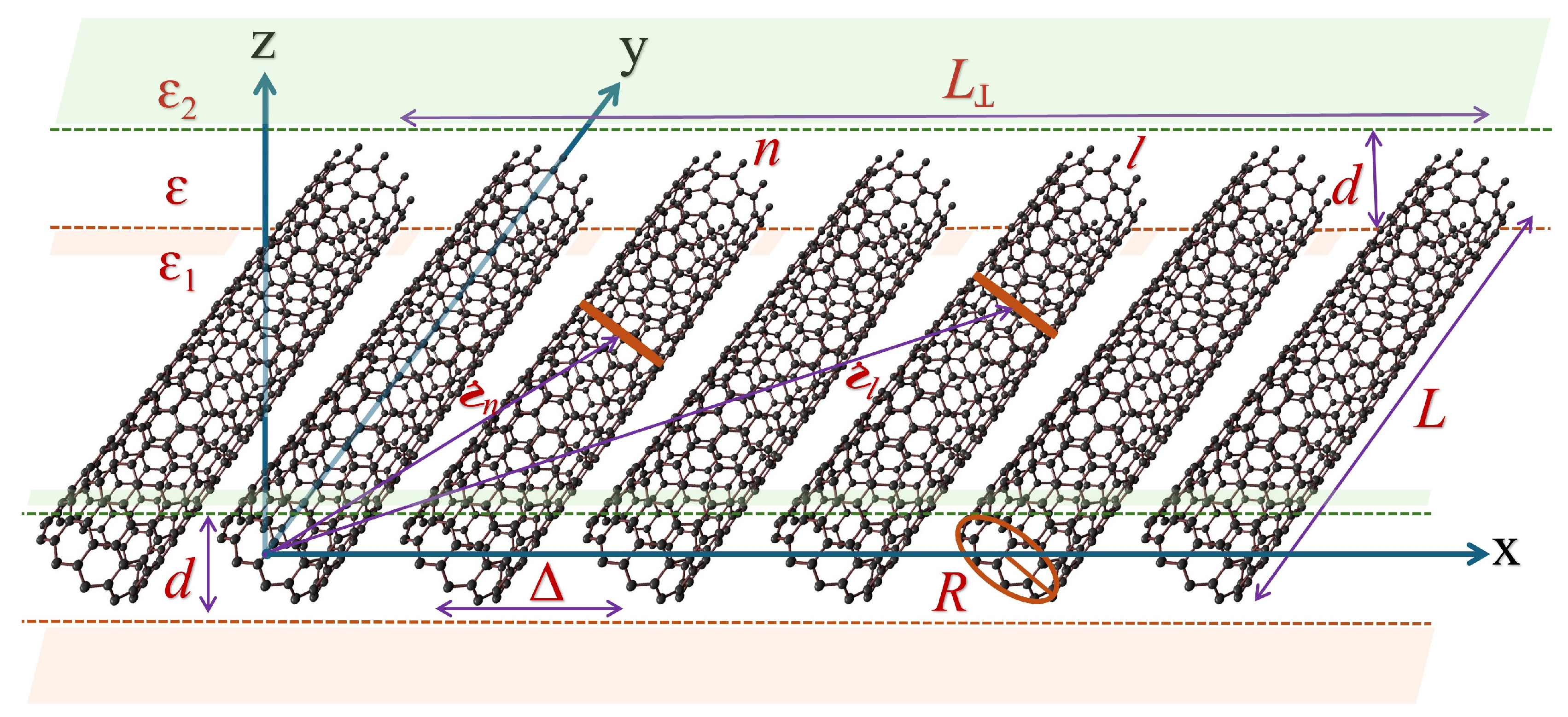
Figure 3.
Dimensionless conductivities of a (9,0) (left panel) and (10,0) (Right panel) SWCNTs along the corresponding CNT axis as a function of photon energy (expressed in eV).
Figure 3.
Dimensionless conductivities of a (9,0) (left panel) and (10,0) (Right panel) SWCNTs along the corresponding CNT axis as a function of photon energy (expressed in eV).
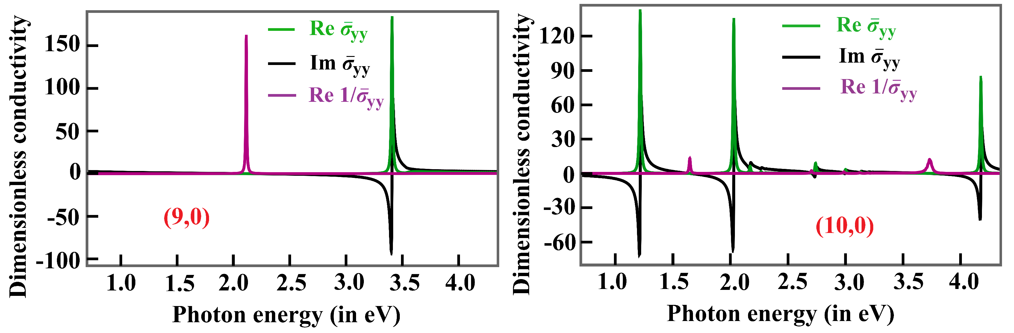
Figure 4.
Dimensionless conductivities and dimensionless dielectric functions of a (11,0) SWCNT along the SWCNT axis plotted as a function of photon energy (expressed in eV). Only the first two excitonic peaks and a plasmonic peak are shown. For better visibility, curves and are scaled by . In the inset, the magnified version of the curves near the resonances of and are shown.
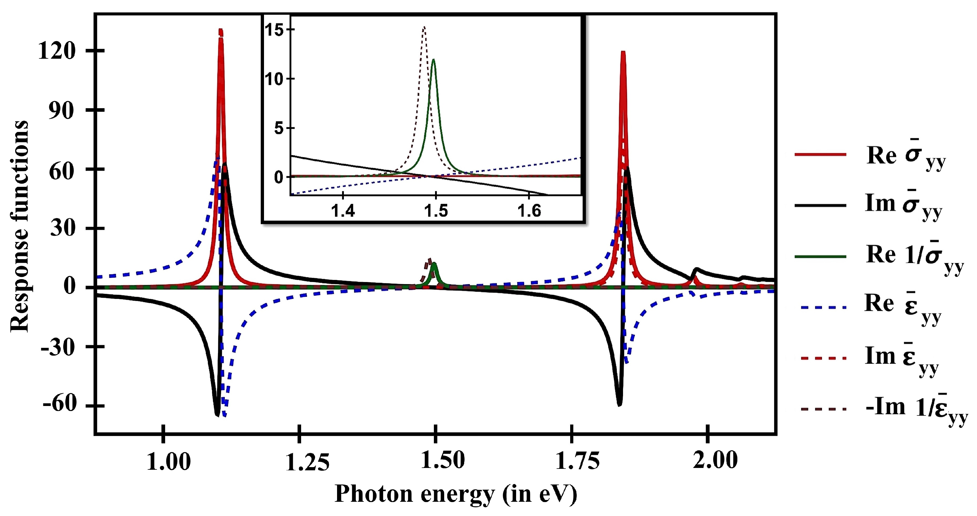
Figure 5.
Dimensionless dielectric responses of a periodic array of (9,0) SWCNTs (left panel) and (10,0) SWCNTs (right panel) along their CNT axis as a function of momentum times radius of respective CNT and the photon energy (expressed in eV). The relative permittivity of the substrate, superstrate, and dielectric medium are taken as 1, 1, and 20, respectively. Only the first resonances of the response functions are shown for (9,0) SWCNT film, while the first two resonances of the response functions are shown for (10,0) SWCNT film. The fractional density parameter is . The red colored surface represents the , the blue colored surface depicts the , and the negative of is shown by green colored surface.
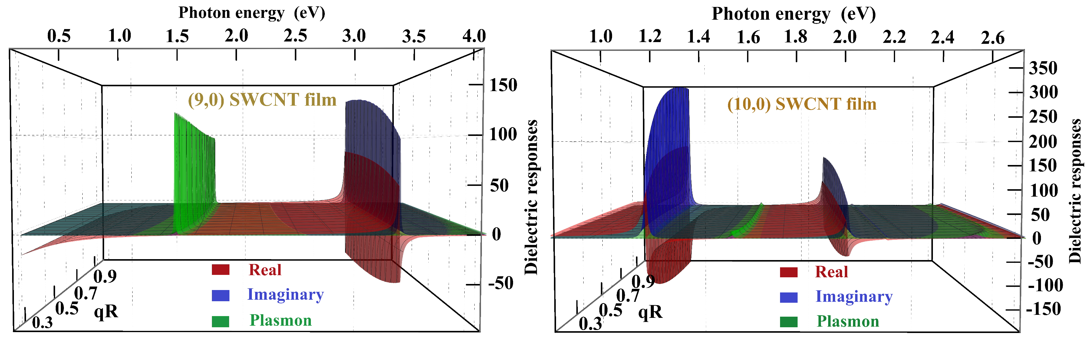
Figure 6.
Dimensionless dielectric functions of a periodic array of (11,0) CNTs along the CNT axis as a function of momentum times radius of (11,0) CNT and the photon energy (expressed in eV). The relative permittivities of the substrate, superstrate, and dielectric medium are taken as 1, 1, and 15, respectively. Only the first resonances of the response functions are shown. Three different scenarios if the values, namely, (a), (b), and (c) are taken. Figure (d) shows the comparison of plasmon spectra only for the cases chosen in (a), (b), and (c).
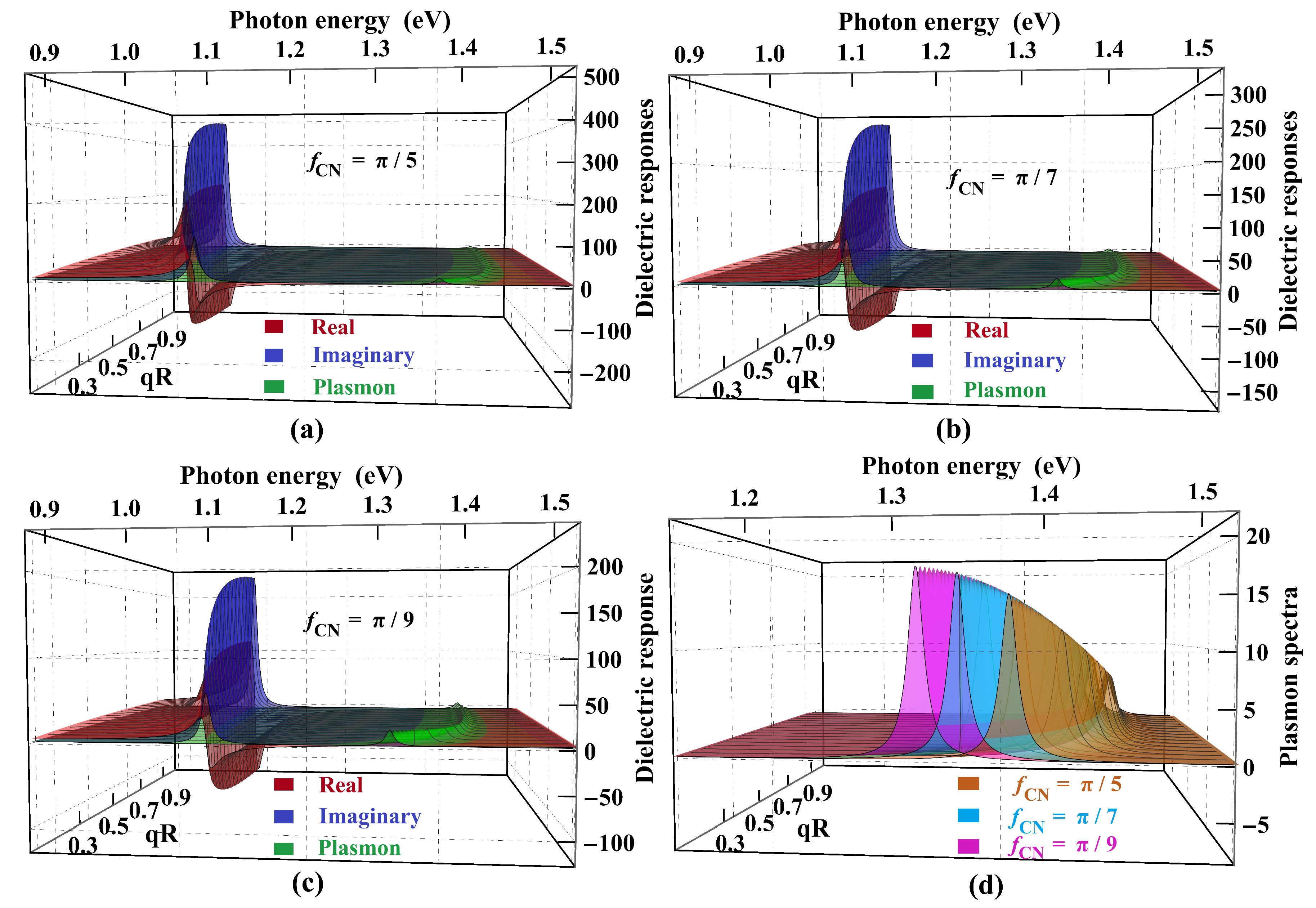
Figure 7.
Dimensionless dielectric responses of an ultrathin array of (11,0) CNTs along the CNT axis as a function of photon energy (expressed in eV) and length of a CNT , (expressed in terms of the circumference of a (11,0) CNT) for the mimimum nonzero momentum . The CNTs are tightly packed, and the thickness of the film equals the diameter of a (11,0) CNT making . The inset shows the geometry related to the SWCNT film.
Disclaimer/Publisher’s Note: The statements, opinions and data contained in all publications are solely those of the individual author(s) and contributor(s) and not of MDPI and/or the editor(s). MDPI and/or the editor(s) disclaim responsibility for any injury to people or property resulting from any ideas, methods, instructions or products referred to in the content. |
© 2025 by the authors. Licensee MDPI, Basel, Switzerland. This article is an open access article distributed under the terms and conditions of the Creative Commons Attribution (CC BY) license (http://creativecommons.org/licenses/by/4.0/).
Copyright: This open access article is published under a Creative Commons CC BY 4.0 license, which permit the free download, distribution, and reuse, provided that the author and preprint are cited in any reuse.


