
Submitted:
26 February 2025
Posted:
27 February 2025
You are already at the latest version
Abstract
This study investigates the mechanical an optical characteristics of silicon nitride thin films deposited with PECVD at 80 °C for tunable SiNx-SiOy based MEMS cavities. By varying the deposition parameters using SiH4 and N2 as precursor gases for SiNx thin films allows to tune the refractive index to a value as high as of 2.398±0.013 at an extinction coefficient of only 0.011, an excellently low surface roughness of only 0.41 nm and a compressive stress about 140 MPa. We deposited a 6.5 layer pairs of SiNx/SiOy distributed Bragg reflector (DBR) micro-electro-mechanical system (MEMS) mirror that covers the whole 1300 and 1550 nm range. Cavity architectures were fabricated in the clean room providing a variety of cavity lengths between 0.615 µm and 2.85 µm. These lengths were then simulated in order to estimate the Young´s Modulus of SiNx, obtaining values from 56-92 GPa.
Keywords:
Silicon nitride
; PECVD
; DBR
; refractive index
; Fabry-Pérot cavity
; extinction coefficient
; Young´s Modulus
; Stress gradient
1. Introduction
Silicon oxide (SiOy) and silicon nitride (SiNx) thin films are implemented in a vast number of application fields. The tailored mechanical and optical characteristics of SiNx make it a material attractive for antireflection-, isolation- and passivation coatings in solar cells and CMOS [1,2], and for waveguides in photonic integrated circuits [3,4]. High quality dielectric isolating materials are further implemented as so-called high-k dielectrics in MOS devices [5]. A key application in the optical domain are Bragg mirrors composed of a low refractive index material, frequently SiOy and a high refractive index material [6]. An alternating multilayer sequence of quarter wavelength layers results in a reflectivity very close to 100% due to constructive interference in reflection, given by the negligible loss of the materials. These mirrors outperform metal mirrors that hardly get beyond 98% reflection, resulting in considerable losses for systems with many mirrors. The larger the refractive index contrast between both dielectrics the larger the block bandwidth. As there are hardly any solid, mechanically stable and low loss materials with a refractive index below that of SiOy (n~1.45), increasing the refractive index contrast of the high index layer is the only viable option for increasing the block band width. Silicon carbide (SiCz) is a sensible option in the visible domain with a refractive index around 2.6 that decreases with increasing wavelength. In the telecom band, however, non-crystalline SiCz as deposited with typical PECVD processes, features non-negligible losses [7], deteriorating the mirror quality.
A further physical parameter that can be utilized in PECVD films to achieve functionality is the tunable stress that allows for implementation in microelectromechanical systems (MEMS) [8,9]. An example of a tunable optical filter is illustrated in Figure 1a). It consists of a MEMS-tuned microcavity where both stress and high refractive index contrast to SiOy are essential in order to obtain a functional device [10,11]. The filter is composed of a Distributed Bragg Reflector (DBR)-based MEMS Fabry-Pérot (FP) cavity, where a temperature- or electro-statically tuned concave Bragg reflector MEMS is grown on top of a static Bragg mirror. The air gap (Lcav) between top and bottom mirror that is achieved by depositing the top Bragg mirror with compressive stress and subsequently releasing it, determines the free spectral range (FSR) of the cavity [12]. For carefully chosen reflectivities of the two Bragg mirrors, the filter structure features a spectrally very sharp, tunable transparent notch within the block band when the effective cavity length Leff equals multiples of a half wavelength as illustrated in Figure 1b). By applying heat or an electrostatic force, the MEMS mirror can be deformed, leading to a change of Lcav and consequently a widely tunable transmission filter. Also here, a large refractive index contrast between the individual Bragg layers has several advantages: (i) much less periods are required to achieve a target block band reflectivity, (ii) a larger block band and free spectral range, (iii) less inertia and thus faster tuning speed in case of electrostatic tuning and (iv) less thermal mass and thus faster tuning speed in case of thermal tuning.
High quality films are frequently deposited with plasma-enhanced chemical vapour deposition (PECVD) that allows to tune the chemical composition as well as the stress of thin films. Low temperature PECVD is essential for deposition of dielectric materials with high thickness precision over temperature-sensitive materials. PECVD deposited SiNx had been studied in terms of refractive index showing results in the telecommunication range from 2 to 2.6 at a chamber temperature of 80°C and even up to 3.08 for higher temperatures [2,3,4]. Thin films of this material have been also characterised in terms of stress gradient, from compressive to tensile values and in Young modulus (E) through various techniques [13,14,15]. Both parameters are essential for designing the MEMS-tuned cavities where the material stress in the MEMS Bragg reflector determines its radius of curvature and the optical parameters its reflectivity and absorptive loss. For cavities with high quality factor as well as for implementation as tuning elements in VCSELs [16] that feature much less gain per round trip as in-plane DFB or DBR lasers, the loss tangent of the material must be as low as possible.
Besides application in lasers, tunable MEMS find their applications spectroscopy, optical communication or optical imaging [17,18,19], amongst others. The MEMS design developed in this study and the desired characteristics are meant for their application in swept source optical coherence tomography (SS-OCT). For this reason, our goal is to design a device with low MEMS mass for fast tuning, wide block band and small cavity length for large free spectral range and low absorption in the 1550 nm range as these parameters will determine the characteristics of the tomographic image [20].
In this study, we first investigate the refractive index, extinction coefficient, the stress gradient and roughness of single silicon-rich SiNx film applying different recipes. Then selecting the most suitable recipe for our application we deposit and characterise a silicon-rich SiNx/SiOy DBR. As final step, we develop a movable membrane with different architectures, selecting one of the designs, we studied its electro-thermal tuning behaviour and through simulations we estimate the Young’s Modulus of silicon-rich SiNx of that specific recipe.
2. Materials and Methods
A Plasmalab 100 ICP 180 from Oxford Instruments Plasma Technologies at a substrate temperature of 80 °C and an inductively coupled plasma (ICP) generator at a radio frequency (RF) of 13.56 MHz with an optional additional RF field between the electrodes is the modular plasma processing system employed in this study. Two inch boron doped (100) silicon wafers with a thickness of 280 μm are used as substrate. We implemented different parameters of gas flow ratio, RF power and chamber pressure as summarized in Table 1, for growth of thin films of silicon-rich SiNx at a deposition duration of 15 minutes. The precursor gases used in this deposition are N2 and SiH4, avoiding the absorption centres that NH3 creates [3].
For every recipe, refractive index (n), extinction coefficient (k) and deposition rate (DR) are determined using ellipsometry (Sentech 850) at an incidence angle of 70°. In this methodology a Cauchy model is employed in order to determinate these parameters [21]. Then, the roughness of the film is measured using a Detak Stylus Profiler, as well as the curvature of the substrate before and after deposition, that allows the evaluation of the stress gradient of the layer using the bending plate method [22].
Once the parameters of refractive index, roughness and stress are determined, applying different processes of etching and evaporation techniques, following a similar protocol to the described in [12], we fabricated on wafer hundreds of MEMS-FP cavities with 9 different architectures. Each of these filters consist on a plane concave cavity formed by a bottom and a top DBR with two different electrodes on top of each mirror. A 6-layer pairs of quarter-wavelength silicon-rich SiNx and SiOy DBR deposited over a double polished substrate of boron doped (100) silicon wafer with a thickness of 280 µm forms the plane part of the cavity. Over this bottom reflector is deposited a second DBR in this case with 6.5-layer pairs and a concave shape, structure that is achieved as a result of the stress gradient of the layers and the chromium sacrificial layer that separates both reflectors during the fabrication process and that allows the final airgap (Lcav). The SiOy layers of both DBR were deposited with a flow of precursor gases 12:3 sccm SiH4:N2O, an IPC power of 500 W, an RF power of 75 W at 7.5 mTorr of chamber pressure. SiOy features a DR of 15.5 nm/min, a refractive index at 1550 nm of n =1.4476 and a compressive stress of 130 MPa. The reflection band of the DBR is measured using ellipsometry at 40°, in this case the angle of measurement is reduced until the minimum achievable by the ellipsometer to have a measurement closer to the 0° as possible.
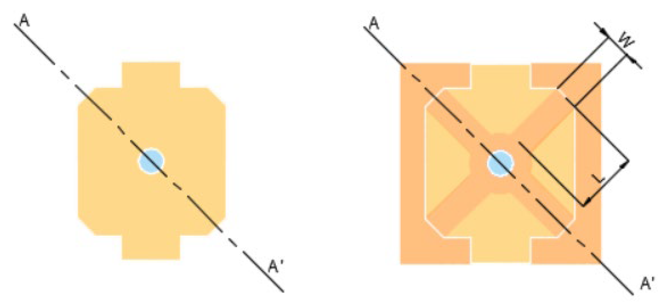
Figure 1 a shows a schematic cross sectional image of a MEMS-FP cavity. The geometry of the FP-cavity bottom and top electrode are illustrated in Figure 2 where the width (W) and length (L) of the arms are altered for every architecture while the central ring in the top electrode that connects the four arms keeps a constant external radius of 40 and an internal of 25 ± 1 μm. This is the optical window.
Figure 2.
Top view schematic representation of a MEMS-FP cavity. On the left: bottom electrode. On the right: complete device with optical window (blue) and top electrode (dark orange).
Figure 2.
Top view schematic representation of a MEMS-FP cavity. On the left: bottom electrode. On the right: complete device with optical window (blue) and top electrode (dark orange).
Using a Detak stylus profilometer we measured the curvature of every architecture. Then the nine architectures are simulated in Comsol Multiphysics that provides the values in Young’s modulus, E, of the silicon-rich SiNx deposited in the DBR assuming a Poisson’s ratio of 0.27 [11].
A CTL 1550 tunable diode laser from Toptica Photonics with a tuning range from 1510 to 1630 nm was used as laser source for the tuning characterization of one of the designs. The laser is focused on the active device that features an optical window diameter of 13.5 µm by a collimator with a focus of 12 mm combined with a micro focus lens of 8mm of focal length. A photodetector captures the transmitted power of the laser through the FP-filter that tunes its whole range at 0.1 nm/s at stable temperature thanks to a Peltier element while different values of current are applied on the top electrode in order to tune the FP-cavity electrothermally.
3. Results
Table 1. shows the precursor gases flow (sccm), the IPC power (W), the RF power (W) and the APC pressure (mTorr) used in every recipe along with the average results of various deposited films in DR (nm/min), stress gradient (MPa), Roughness, refractive index n and extinction coefficient k at 1550 nm.
The design goal of the recipe is to achieve an as high as possible refractive index, a k-value below 0.0124 and a compressive stress inferior to 150 MPa in order to overcompensate the stress of the SiOy quarter wavelength layers of about 100 MPa compressive. These characteristics are necessary to achieve functional MEMS mirrors in mechanical and optical terms. The limit for the extinction factor is chosen such that the absorption constant at 1550 nm, is below 1000/cm. The roughness should be as low as possible while the deposition rate is secondary. First, we determined approximate process parameters in preliminary work (not shown here). Table 1 shows the final optimization step.
In Table 1 the recipes can be classified in two groups, in the first one (recipes 1 to 3) the flow volume of SiH4 is of 9.8 sccm, and the second one (recipes 4 to 7) with 9.6 sccm of SiH4. In both groups the roughness increases dramatically when RF power is introduced while the refractive index, stress gradient and the deposition rate increase while the extinction coefficient decreases (recipe 2 and 6). In deposition 3 the APC pressure was reduced by 0.3 mTorr giving as a result a decrease in the refractive index and an increase in stress with respect to deposition 1 and 2. A similar situation occurs in deposition 4 where the APC pressure is decreased in 2 mTorr compared to recipe 5, in this case both refractive index and stress show a rise. On the other hand when this pressure is increased (recipe 7) both refractive index and stress are reduced.
From all the seven recipes depositions 2 and 4 show the optical and mechanical characteristics that are best suited for the MEMS. Although their characteristics are very similar, both have a high refractive index, a low absorption and their stress gradient is inside the desired boundaries, recipe 2 was dismissed due to its high roughness. Being recipe 4 the material selected for the fabrication of the FP-filter reflectors.
Figure 2 shows the measured reflectivity of a 6.5 layers pairs silicon-rich SiNx/SiOy DBR deposited with the silicon-rich SiNx deposition parameters 4 in Table 1 and the parameters described for SiOy in the methods section. This reflection corresponds to the top-DBR of the FP-filters described in this manuscript. The expected total thickness is 2716 nm. The π-polarisation provides a refection band (R>0.96) in the range from 1140 to 1620 nm and in the case of σ-polarisation this range goes from 1220 to 1480 nm.
Figure 2.
Reflectivity measurement of 6.5 layer pair silicon-rich SiNx/SiOy under an incidence angle of 40°.
Figure 2.
Reflectivity measurement of 6.5 layer pair silicon-rich SiNx/SiOy under an incidence angle of 40°.
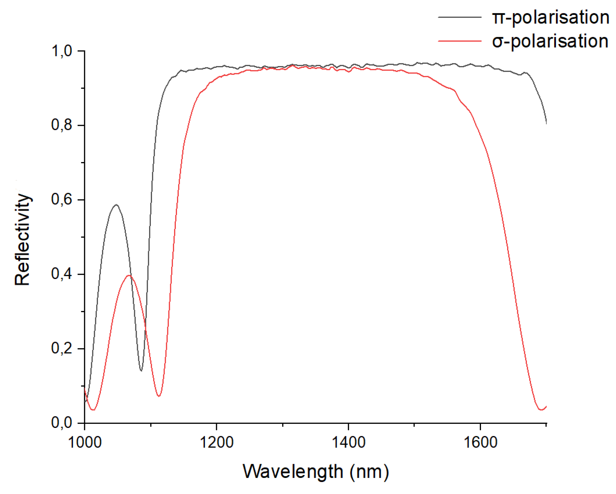
Table 2 summarizes the 9 different architectures for our MEMS ordered from smaller to larger electrode area, the cavity length (Lcav) in nm and Young´s modulus E in GPa.
The cavity length, i.e. the distance between the MEMS mirror and the bottom Bragg mirror depends on the MEMS architecture, where W and L produce an important influence. Particularly, short lengths L decrease the air gap in the cavity, producing that Lcav varies from 614 to 2850 nm. The simulation provides an E ~80±12 GPa, averaged over all samples.
Figure 3 shows the tunability in transmission for a FP-cavity with 23 µm long and 33 µm wide arms, corresponding to a cavity length of 651 nm (c.f. table 2). At zero bias, the main transmission resonance is centered at 1542.9 nm, i.e. in the middle of the C band. Upon thermal tuning, the main transmission peak shifts out of the range covered by the tunable diode laser, yet reaching a peak wavelength of 1629.6 nm at a tuning current applied to the top electrode of 60 mA while keeping a constant base temperature of 16°C. The full width half maximum of 0.70 ± 0.1 nm as average of all the peaks shown in the figure.
4. Discussion
From the seven recipes of Table 1 we find the higher refractive index in recipes 2 and 6, in both recipes RF power is introduced into the process. This produces an increase in the refractive index, the deposition rate, the compressive stress and the roughness of the thin film. This last parameter, the roughness, makes these thin films inappropriate to be used for the DBR deposition due to the high number of defects that it creates, even if the stress characteristics and the extinction coefficient fit our objectives. These changes occur because the RF power potentiates the attraction of the plasma generated in the ICP coils to the substrate during deposition creating a denser plasma at the sample surface [3,9,23].
In our investigation the ratio between the recipes is very similar, so one could think that the increment of the ratio between precursor gases could be a way to achieve a higher refractive index as discussed in refs. [3,24]. But as side-effect this also leads to an increase of the layer compressive stress which is not desirable for the mechanical behaviour of the MEMS [9]. In recipes 3 and 4 the APC pressure is reduced and increased in case of recipe 7, producing a more compressive stressed film when this parameter is reduced and more tensile when it is increased. In recipes 3 and 7 the refractive index suffers a reduction in comparison with the original recipe (1 and 5), however in recipe 4 this parameter shows a rise, this occurs because there is a relation between the correct amount of precursor gases and the chamber pressure to obtain a balance between refractive index and stress gradient [1]. In this case, recipe 3 is discarded because of its stress and 7 shows the lowest refractive index of all investigated recipes.
This led us to choose recipe 4 to be employed for the DBRs that form the FP filter. It provides a much higher refractive index as compared to stochiometric Si3N4 (n~1.95) and sufficiently low extinction coefficient while keeping its stress inside the required parameters that allow functional MEMS. Other studies have achieved higher refractive index with the same deposition temperature and precursor gases as in [2] where the refractive index has a maximum value of 2.6. Nevertheless this study used low pressures that are not achievable with the PECVD machine employed in our study, and also RF power that as already mentioned causes excessive film roughness, incompatible with DBR deposition.
Figure 2 shows the reflectivity band of the FP-filters top DBR, that covers two important wavelength ranges as 1310 and 1550 nm. Using the matrix method the theoretical reflectivity and stopband of this DBR is of 0.997 and 510nm respectively under vertical incidence. The ellipsometric measurements shows inferior results, this is because of the angle at which ellipsometry was performed makes the reflectivity band less broad than it would be at 0° measurement and also it produces that its centre wavelength is slightly moved to shorter wavelengths as described in [25]. A similar work on DBR was performed by [9] though with different reflectance band centre. This study used PECVD at 75 °C with no RF power obtaining values of stress that flows from compressive to tensile with a refractive index in the 1550 nm range of about 2 using the same precursor gases that were applied in our depositions. It shows a reflective band of 260 nm that is almost half of the bandwidth achieved in this manuscript in π-polarisation using 11.5 layers of SiNx/SiOy. In our study the number of layers is about halved for the same reflectivity because the refractive index difference between our layers is almost 20% higher than in the mentioned study. This optimization compared with previous work is beneficial in terms of increment of tuning speed and FSR of the MEMS devices due to the reduction in mass and in cavity length [12,26].
Besides obtaining a reduction in the top electrode mass and cavity length due to changes in the MEMS composition, their geometry also plays an important role in the optimization of these characteristics. As Table 2 shows, the length of the cavity increases as the width and the length of their arms does. This table also illustrates the results on Young´s modulus product of the finite element simulation of every architecture. These results are lower compared with [11] where SiH4/NH3/N2 were used as precursor gases and a Young’s modulus in the range between 240-320 GPa was calculated by membrane point deflection with a substrate temperature of 300 °C. Such high values would lead to excessively large Lcav and thus reduced free spectral range. Results in the same range applying nanoindentation methods and using SiH4/NH3/N2 as precursor gases was obtained in [15], a study that also demonstrates how the value of E is affected by the substrate temperature. The nanoindentation method was also applied in [8] where an E of 97 GPa at 125°C of deposition was obtained. To our knowledge there is no study in E where SiH4/N2 were used as precursor gases at temperatures inferior to the already cited. Taking into account the mentioned studies, the increase of Young’s modulus with the substrate temperature and with the increase of H-N bonds that the use of NH3 introduces, the results of our study are reasonable [27].
Figure 3 shows the electro-thermal tunability characterisation of one of the fabricated architectures. By comparing to Figure 1, we actually expect a single peak. The further resonances besides the main resonance appear most likely because of imperfect coupling to the resonator, possibly exciting undesired modes with light outside the central hole of the main cavity. Their amplitude can be reduced by improved coupling schemes, exactly matching the window size and required NA of the filter. This goes beyond the investigations in this manuscript. For applications in a laser, only the dominant mode will survive as long as there is sufficient gain.
The main peak reaches the maximum tuning wavelength of the CTL by applying a at a current of 60 mA through the top electrode. The investigated device shows a tuning range of 86.7 nm already as compared to the case without any tuning current. The rupture limit of this device is 80 mA, determined by destroying several devices. For the maximum tolerable current, we expect a tuning range beyond 150 nm, to date only achievable with external, grating-tuned cavities that are orders of magnitude larger than the demonstrated device. We remark, however, that the currently investigated device may already reach the end of the stop band at 80 mA tuning current. The wavelength at 0 mA tuning current (being in the midst of the stop band of the investigated device) can be tuned by the cavity length during manufacturing and fine-tuned during experiments by the base temperature, allowing full use of the maximum tunability.
As the cavity size of the order of 650 nm is several times smaller than MEMS-tuned cavities investigated in vertical cavity diode lasers (VCSELs) with a demonstrated tuning range of 103 nm [16], we do not expect any mode hops within this tuning range. This is supported by the fact that no new modes arise at the lower tuning end of the CTL when the current is increased until the rupture limit of the cavity .The tuning continues towards wavelengths higher than 1630 nm as it was already expected from the simulation of Figure 1b, the reflectivity profile of Figure 2 and the theoretical reflectivity mentioned in the results section calculated by the matrix method. Other authors have achieved with DBR based FP-filters 112 nm in terms of wavelength tuning by employing similar kind of dielectric materials [26]. Other more complex and bulk MEMS designs in the near infrared region can tune from 1479 to 1590 nm as in [28] in this case avoiding the mechanical disturbances that suspended multilayer MEMS suffer, yet still considerably less than the extrapolated tuning range of 150 nm reported in this manuscript.
5. Conclusion
This work reports the study of low temperature deposited PECVD Silicon-rich SiNx thin films. These films were characterised in terms of refractive index, extinction coefficient and stress gradient for different deposition conditions. The most adequate recipe was then employed to form a silicon-rich SiNx/SiOy DBR with a broad band reflection centred at 1400 nm with a stop band width of about 370 nm. The mechanical characteristics of SiNx were essential in order to fabricate a DBR-FP filter that forms a suspended membrane structure supported by 4 arms, as these characteristics define the distortion of the membrane and affect the performance of the filter. The MEMS-FP filters were fabricated with different geometries, providing each of them a different cavity length. The cavity lengths obtained from about 650 to 2850 nm translate in a FSR at 1550nm larger than 400nm, i.e. slightly larger than the block band size (~370 nm), a fact of high importance for tunable, single-moded filters in order to achieve mode-hop free tuning.
Of all the nine fabricated designs one of them was selected to be characterised electro-thermally. By applying current from 0 to 60 mA, the studied FP-filter achieves a tuning range of almost 90 nm centred at 1585 nm of wavelength. We expect a tuning range of at least 150 nm by applying the maximum permissible current of 80 mA before thermal destruction of the mirror occurs.
As a final step, using the cavity length of every fabricated filter into a finite element software we estimated a Young´s modulus of SiNx from 56 to 90GPa with an average value of 80 GPa. The results obtained in this study are essential to investigate new geometries that could improve the performance of MEMS-FP filters and will allow more precise simulations.
Acknowledgments
Marie Curie Actions. Horizon 2020. NETLAS. Grant agreement 860807.
References
- N. Hegedüs, K. Balázsi and C. Balázsi. Silicon Niride and Hydrogenated Silicon Nitride Thin Films: A Review of Fabrication Methods and Applications. Materials 2021, 14, no. 5658. [CrossRef]
- G. Suchaneck, V. Norkus and G. Gerlach. Low-temperature PECVD-deposited silicon nitride thin films for sensor application. Surface and Coating Technology 2001, 142-144, 808-812. [CrossRef]
- Doris K. T. Ng, Q. Wang, T. Wang, S. K. Ng, Y. T. Toh, K.P. Lim, Y. Yang and D. T. H. Tan. Exploring High Refractive Index Silicon-Rich Nitride Films by Low-Temperature Inductively Coupled Plasma Chemical Vapor Deposition and Applications for Integrared Waveguides. Applied Materials and interfaces 2015, 7, 21884-21889. [CrossRef]
- D. H. Yoon, S. G. Yoon and Y. Kim. Refractive index and etched structure of silicon nitride waveguides fabricated by PECVD. Thin Solid Films 2007, 515, 5004-5007. [CrossRef]
- Liu, L.N.; Tang, W.M.; Lai, P.T. Advances in La-Based High-k Dielectrics for MOS Applications. Coatings 2019, 9, 217. [CrossRef]
- F. Réveret, L. Bignet, W. Zhigang, X. Lafosse, G. Patriarche, P. Disseix and F. Médard. High reflectance dielectric distributed Bragg reflectors for near ultra-violet planar microcavities: SiO2/HfO2 versus SiO2/SiNx. J. Appl. Phys 2016, 9,120. [CrossRef]
- J. Cesar. SiOx-SiCz MEMS-DBR-Based Tunable Optical Devices. Doctoral Thesis, Technical university of Darmstadt; Merckstrasse 25, Darmstadt, 64283 Germany. 25 June 2020.
- H. Huang, K. Winchester, X. Y. Liu, Z. Hu, C. A. Musca, J. M. Dell and L. Faraone. Determination of mechanical properties of PECVD silicon nitride films for tunable MEMS Fabry-Pérot optical filters. J. Micromech. Microemg 2005, 15, 608-614. [CrossRef]
- Z. Shao, Y. Chen, H. Chen, Y. Zhang, F. Zahn, J. Jiam, Z. Fan, L. Liu, C. Yang, L. Zhou and S. Yu. Ultra-low temperature silicon nitride photonic integration platform. Opt. Express 2016, 24, 1865-1872. [CrossRef]
- K. J. Winchester and J. Dell. Tunable Fabry-Pérot cavities fabricated from PECVD silicon nitride employing zinc sulphide as the sacrificial layer. J. Micromecha. Microeng 2001, 11, 589-594. [CrossRef]
- Z. Gan, C. Wang and Z. Chen. Material Structure and Mechanical Properties of Silicon Nitride and Silicon Oxynitride Thin Films Deposited by Plasma Enhanced Chemical Vapor Deposition. Surfaces 2018, 1, 59-72. [CrossRef]
- C. Gierl, T. Gruendl, P. Debernardi, K. Zogal, C. Grasse, H. A. Davani, G. Böhm, S. Jatta, F. Küppers, P. Meißner and M. Amann. Surface micromachined tunable 1.55 μm-VCSEL with 102 nm continuous single-mode tuning. Opt. Express 2011, 19, 17336-17343. [CrossRef]
- S.Paul, C. Gierl, J. Cesar, M. Malekizandi, B. Kögel, C. Neumeyr, M. Ortsiefer and F. Küppers. 10Gbit/s Direct Modulation of Widely Tunable. IEEE Journal of selected topics in quantum electronics 2015, 21, 436-443. [CrossRef]
- A.Bagolini, A. Picciotto, M. Crivellari, P. Conci and P. Bellutti. PECVD silicon-rich nitride and low stress nitride films mechanical characterisation using membrane load deflection. J. Micromech. Microeng 2016, 26. [CrossRef]
- H. Huang, K. Winchester, J. Antoszewski, T. Nguyun, B. W. M. Martyniuk, Y. Li, X. Z. Hu, C. A. Musca, J. Dell and L. Faraone. Evaluation of Elastic Modulus and Stress Gradient of PECVD Silicon Nitride Thin Films. Structural Integrity and Fracture International Conference, Brisbane, Australia, 26-29 September 2004.
- H. Huang, K. Winchester, A. Suvorova, B. Lawne, Y. Liud, X. Hud, J. Dell and L. Faraone. Effect of deposition conditions on mechanical properties of low-temperature PECVD silicon nitride films. Materials Science and Engineering A 2006, 435-436, 453–459, 2006. [CrossRef]
- Martin Ebermann, Norbert Neumann, Karla Hiller, Mario Seifert, Marco Meinig, and Steffen Kurth. Tunable MEMS Fabry-Pérot filters for infrared microspectrometers: a review. Proc. SPIE 2016, 9760, 64-83. [CrossRef]
- M. T. Haidar, S. Preu, S. Paul, C. Gierl, J. Cesar, A. Emsia and F. Küppers. Widely tunable telecom MEMS-VCSEL for terahertz photomixing. Optics Letters 2015, 40, 4428-4431. [CrossRef]
- Grulkowski, J. J. Liu, B. Potsaid, V. Jayaraman, C. D. Lu, J. Jiang, A. E. Cable, J. S. Duker and J. G. Fujimoto. Retinal, anterior segment and full eye imaging using ultrahigh speed swept source OCT with vertical-cavity surface emitting lasers. Biomed. Opt. Expres 2012, 3, 2733-2751. [CrossRef]
- Podoleanu. Optical Coherent Tomography. Journal of Microscopy 2012, 247, 209-219. [CrossRef]
- D. Shah, D. I. Patel, J. N. Hilfiker and M. R. Linford1. A Tutorial on Spectroscopic Ellipsometry (SE), 2. The Cauchy Model. Vacumm Technology and Coating 2019, 29-33.
- Brian D. Harper and Wu Chih-Ping. A geometrically nonlinear model for predicting the intrinsic film stress by the bending-plate method. International Journal of Solids and Structures 1990, 26, 511-525. [CrossRef]
- E. Sleeckx, M. Schaekers, X. Shi, E. Kunnen, B. Degroote, M. Jurczak, M. de Potter de ten Broeck and E. Augendre. Optimization of low temperature silicon nitride processes for improvement of device performance. Microelectronics Reliability 2005, 45, 865-868. [CrossRef]
- Fouad Karouta, K. Vora, J. Tian and C. Jagadish. Structural, compositional and optical properties of PECVD silicon nitride layers. J. Phys. D: Appl. Phys 2012, 45. [CrossRef]
- H. Ying-Shin, S. Hu, C. Huang, Y. Lee, J. Lee, C. Chang, Z. Wun and K. Tiong. Incident-Angle-Dependent Reflectance in Distributed Bragg Reflectors Fabricated from ZnO/MgO Multilayer Film. Opt Rev 2014, 21, 651-654. [CrossRef]
- C. Gierl, K. Zogal, H. A. Davani and P. Meissner. Electro thermal and electro statical actuation of a surface micromachined tunable Fabry-Pérot filter. Quantum Electronics and Laser Science Conference, Baltimore, Maryland, USA, 1-6 May 2011. [CrossRef]
- A. Taylor. The mechanical properties and microstructure of plasma enhanced chemical vapor deposited silicon nitride thin films. J. Vac. Sci. Technol. A 1991, 9, 2464–2468. [CrossRef]
- T. Yamanoi, T. Endo, H Toshiyoshi. A hybrid-assembled MEMS Fabry-Pérot wavelength tunable filter. Sensors and Actuators A: Physical. 2008, 145-146,116-122. [CrossRef]
Figure 1.
a) Schematic cross sectional image of a MEMS-FP cavity. b) Simulated filter transmission spectrum for a 6.5-6 mirror pair Bragg cavity with n(SiOy=1.447) and n(silicon-rich SiNx)=2.389 with an air gap of 1µm. The wavelength of the transmission notch can be tuned by the gap size Lcav.
Figure 1.
a) Schematic cross sectional image of a MEMS-FP cavity. b) Simulated filter transmission spectrum for a 6.5-6 mirror pair Bragg cavity with n(SiOy=1.447) and n(silicon-rich SiNx)=2.389 with an air gap of 1µm. The wavelength of the transmission notch can be tuned by the gap size Lcav.
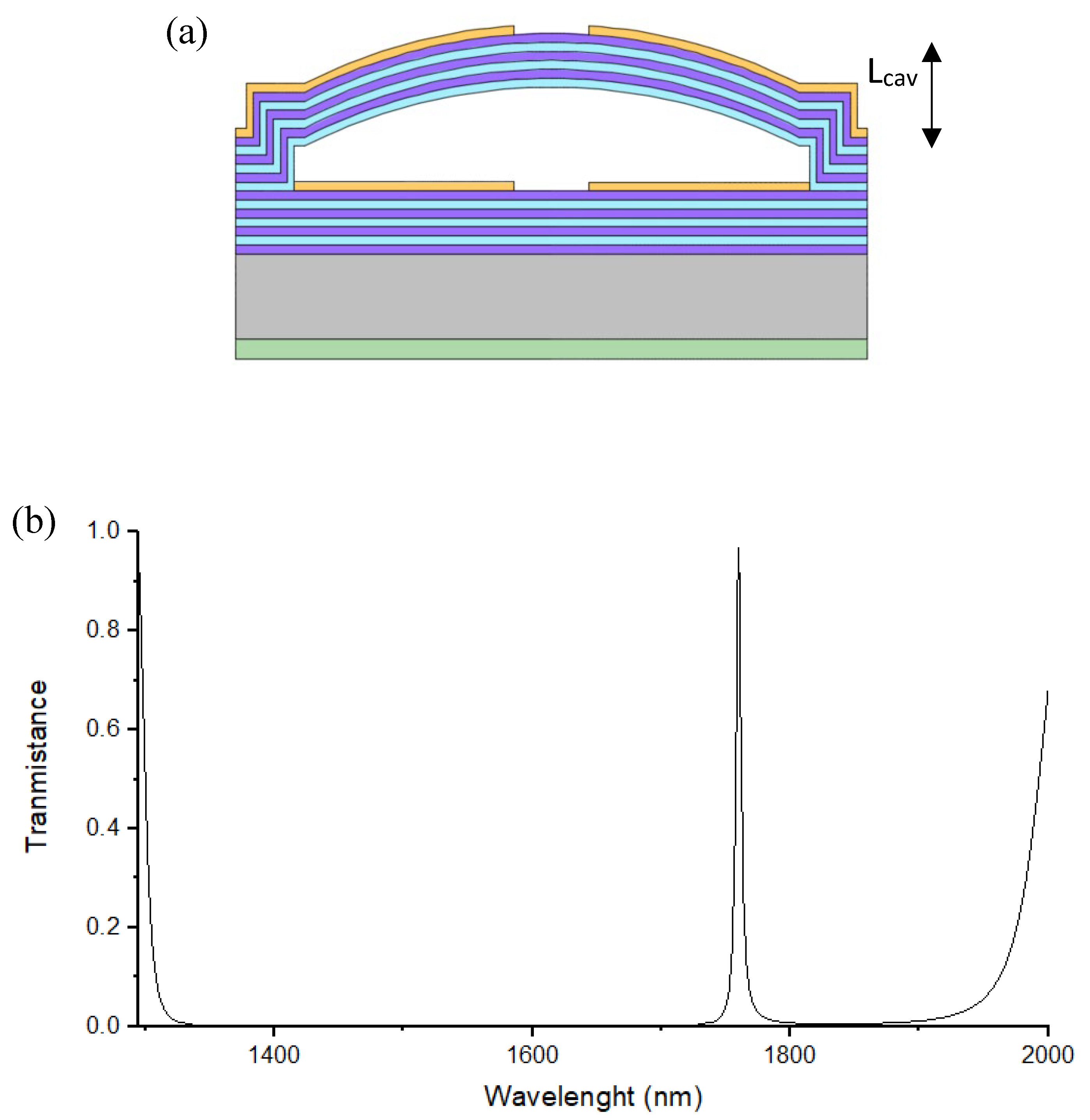
Figure 3.
Transmission spectra for different tuning currents of a FP-filter with and arm width of W=33µm and a length L=23µm.
Figure 3.
Transmission spectra for different tuning currents of a FP-filter with and arm width of W=33µm and a length L=23µm.
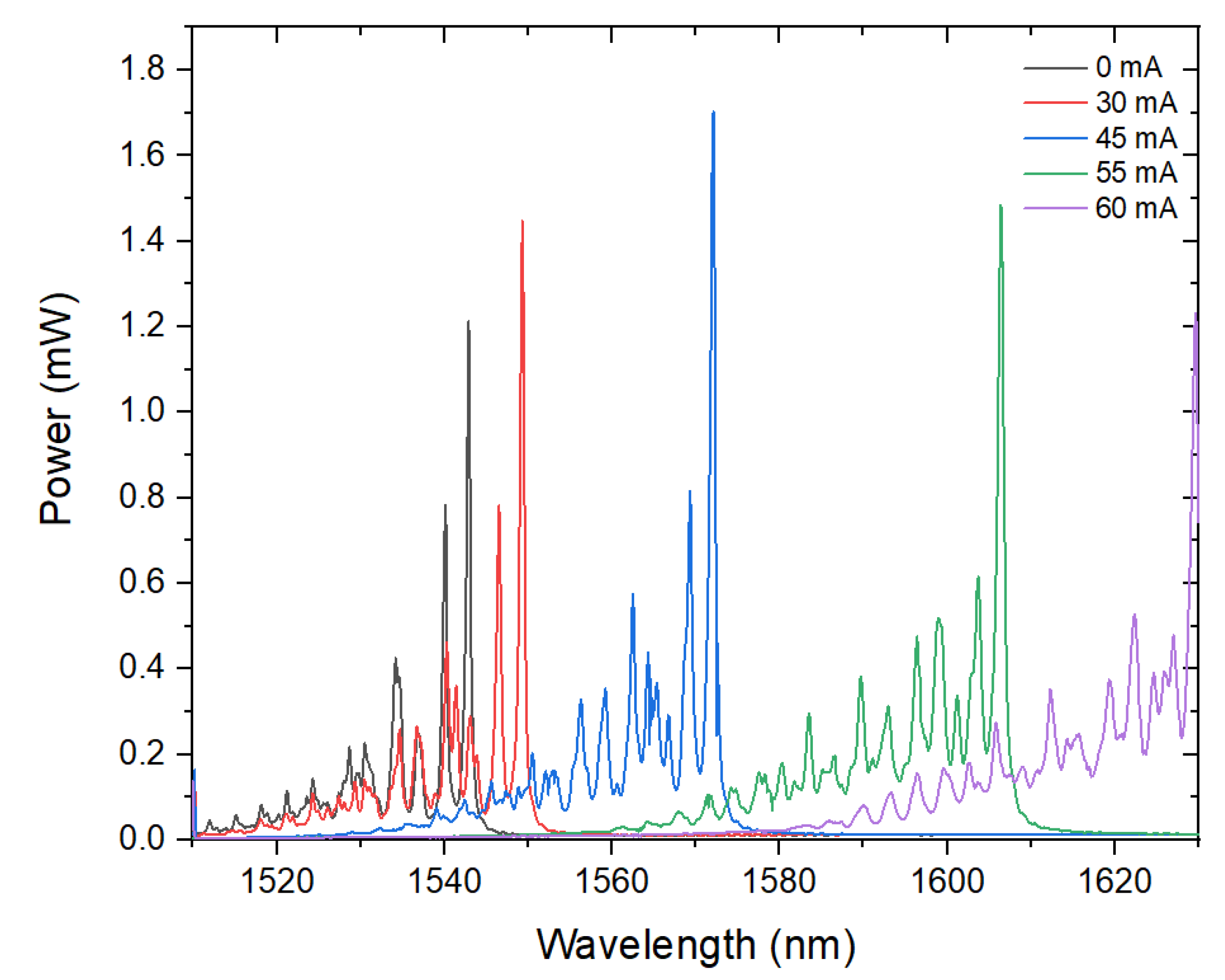

Table 1.
Deposition parameters of silicon-rich SiNx and their results in refractive index, coefficient, stress gradient and roughness. Negative stress denotes compressive.
Table 1.
Deposition parameters of silicon-rich SiNx and their results in refractive index, coefficient, stress gradient and roughness. Negative stress denotes compressive.
| Parameters | 1 | 2 | 3 | 4 | 5 | 6 | 7 |
|---|---|---|---|---|---|---|---|
| SiH4 (sccm) | 9.8 | 9.8 | 9.8 | 9.6 | 9.6 | 9.6 | 9.6 |
| N2 (sccm) | 6 | 6 | 6 | 6 | 6 | 6 | 6 |
| ICP (W) | 200 | 200 | 200 | 200 | 200 | 200 | 200 |
| RF (W) | 0 | 10 | 0 | 0 | 0 | 5 | 0 |
| APC (mTorr) | 7.9 | 7.9 | 7.6 | 6 | 8 | 8 | 8.2 |
| DR (nm/min) | 17.88 | 18.80 | 17.64 | 16.66 | 17.50 | 18.90 | 18.70 |
| n ± 0.013 | 2.398 | 2.498 | 2.378 | 2.443 | 2.385 | 2.449 | 2.293 |
| k ± 0.006 | 0.011 | 0.008 | 0.030 | 0.006 | 0.032 | 0.020 | 0.018 |
| Stress (MPa) | -138 | -152 | -172 | -150 | -135 | -157 | -118 |
| Roughness (nm) | 0.41 | 4.5 | 0.91 | 0.26 | 0.23 | 4.4 | 0.53 |
Table 2.
List of architecture parameters of MEMS, cavity length in every case and estimated elastic modulus.
Table 2.
List of architecture parameters of MEMS, cavity length in every case and estimated elastic modulus.
| W ± 0.25 (µm) |
L ±0.25 (µm) |
Lcav ± 30 (nm) |
E ± 12(GPa) |
|---|---|---|---|
| 33 | 18 | 614 | 56 |
| 33 | 23 | 651 | 63 |
| 48 | 18 | 1485 | 80 |
| 33 | 28 | 733 | 70 |
| 48 | 23 | 1635 | 88 |
| 63 | 18 | 2685 | 89 |
| 48 | 28 | 1725 | 90 |
| 63 | 23 | 2770 | 90 |
| 63 | 28 | 2850 | 92 |
Disclaimer/Publisher’s Note: The statements, opinions and data contained in all publications are solely those of the individual author(s) and contributor(s) and not of MDPI and/or the editor(s). MDPI and/or the editor(s) disclaim responsibility for any injury to people or property resulting from any ideas, methods, instructions or products referred to in the content. |
© 2025 by the authors. Licensee MDPI, Basel, Switzerland. This article is an open access article distributed under the terms and conditions of the Creative Commons Attribution (CC BY) license (http://creativecommons.org/licenses/by/4.0/).
Copyright: This open access article is published under a Creative Commons CC BY 4.0 license, which permit the free download, distribution, and reuse, provided that the author and preprint are cited in any reuse.


