1. Introduction
By virtue of its high transparency in the visible region, titanium dioxide (TiO
2) is widely used in optical and protective applications [
1]. Thin films of TiO
2 are also used as catalysis [
2], optical coating, gas sensors [
3] and many electronic devices [
4]. Numerous techniques have been utilized in synthesis of thin films of TiO
2 namely, sol-gel technique [
5,
6], chemical vapor deposition technique [
7] and chemical bath deposition method [
8,
9], atomic layer deposition method [
10], evaporation technique [
11], reactive sputtering techniques [
12,
13], ion beam assisted method [
14] and pulse laser deposition method [
15]. TiO
2 photo electrode is main component of dye sensitized solar cell (DSSC) which was fabricated first time in 1991 by Regan & Gratzel [
16].
The physical properties of the TiO
2 thin film largely depend upon the method used for synthesis and temperature for annealing. With respect to annealing temperature, authors have documented changes to the structural and optical characteristics of TiO
2 thin films. [
17,
18,
19].
In the present study we have report synthesis of TiO2 thin films by chemical bath deposition method on glass/FTO substrate. Later this thin film was subjected to various characterization techniques for investigation of structural, optical, morphological and photoelectrochemical properties.
2. Materials and Methods
To deposit a thin film of titanium dioxide (TiO2), a precursor solution was prepared using titanium oxysulphate (TiOSO4) using double distilled water (DDW), ethylenediaminetetraacetic acid (EDTA) as complexing agent. Apart from this triton X-100 was added to the precursor to reduce the surface tension.
Titanium oxysulfate (TiOSO4) powder (0.7197 g) was added to 50 mL of DDW. The resulting precursor was stirred magnetically at room temperature for 30 minutes. This process induced a visual change in the precursor solution from a cloudy to a translucent state, indicative of initial TiOSO4 hydrolysis. Subsequently, 1.86 g of EDTA was incorporated into the precursor solution. This addition established a 1:1 molar ratio between TiOSO4 and EDTA, with EDTA functioning as a complexing agent to modulate the subsequent hydrolysis and condensation reactions leading to TiO2 formation. To further modify the solution’s properties, specifically to reduce surface tension, 0.025 mL of Triton X-100 was introduced using a micropipette. The solution was then stirred for an additional 15 minutes, resulting in increased transparency. The pH of the final precursor solution was measured and determined to be within the range of 5 to 6.
A glass substrate measuring 25mm x 25mm x 2.2mm (L x B x W) was selected for the deposition process. Prior to deposition, the glass substrate underwent a cleaning procedure. Initially, it was cleansed with detergent followed by rinsing with DDW. Subsequently, the substrate was immersed in 50% ethanol solution, rinsed again in DDW, and finally dried in ambient air. The same cleaning procedure was applied to a fluorine-doped tin oxide (FTO) glass substrate, which was specifically utilized for depositing TiO2 thin films intended for the investigation of photoelectrochemical properties.
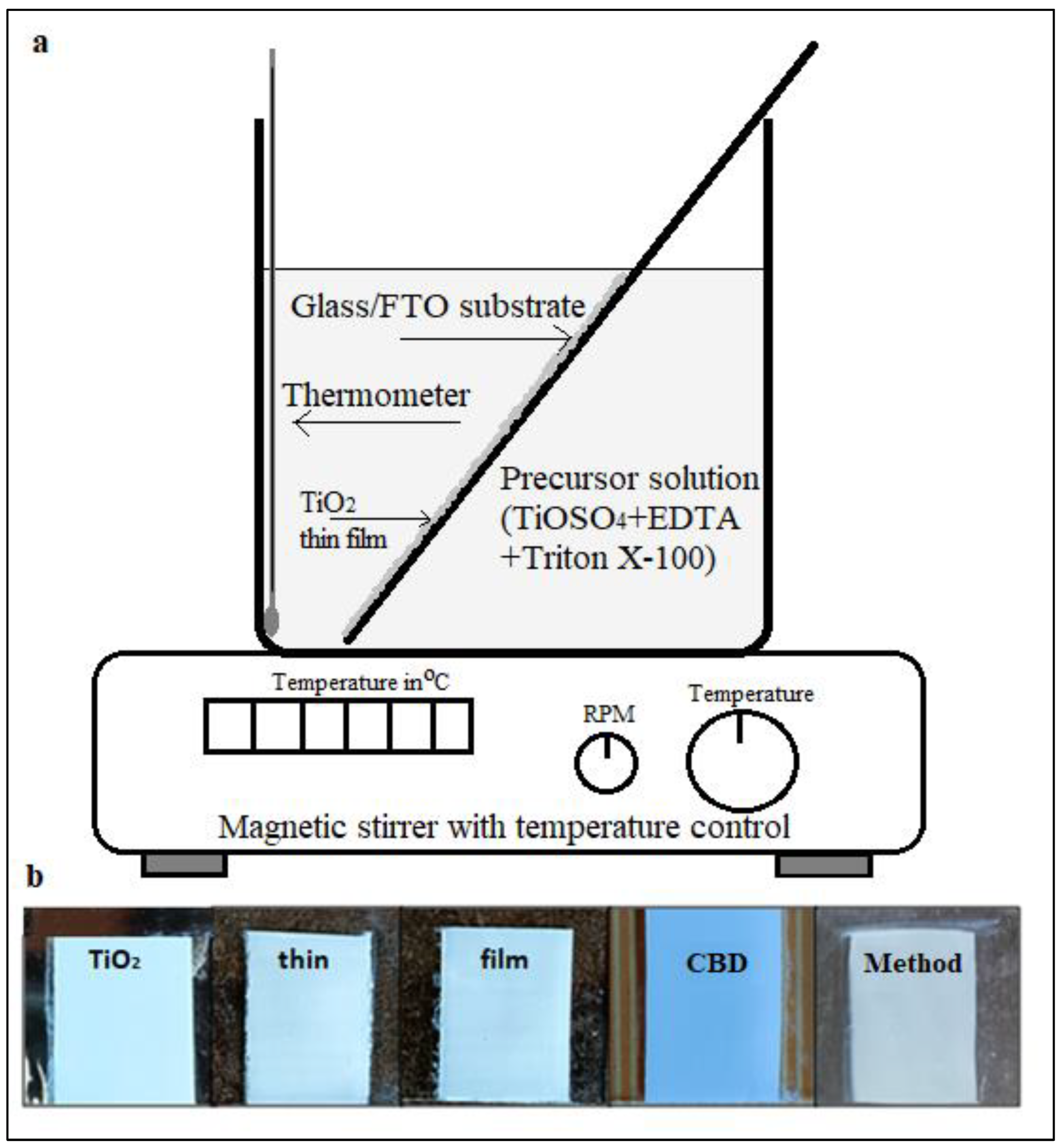
For the deposition of TiO2 thin films via chemical bath deposition (CBD) method, cleaned glass/FTO substrates were immersed in the prepared precursor solution as shown in
Figure 1 (a). The substrates were positioned at an approximate 45° angle relative to the horizontal within the bath. The deposition process was conducted at room temperature. Initial film formation was observed after a 2-hour period, marked by a transition in the substrate’s appearance from transparent to a cloudy white. The substrates remained in the bath for a total of 24 hours. Following deposition, the substrates were rinsed twice with DDW to eliminate any loosely bound particles. The resulting TiO2 thin films exhibited a white color and demonstrated good adherence to the substrates. The deposited TiO
2 thin film displayed a smooth surface without any visible cracks or comet-like structures, as depicted in
Figure 1b. Following the deposition process, the thin film was air-dried for 10 minutes and subsequently annealed in a muffle furnace at 400°C for 30 minutes, with a heating rate of 100°C per 30 minute. The annealing process enhanced the film’s adherence to the substrate, and the resulting TiO
2 thin film remained white in color.
Figure 1b provides actual images of the TiO
2 thin films deposited using the CBD technique.
For the electrochemical impedance spectroscopic study and photoelectrochemical analysis, a polysulfide electrolyte was prepared by dissolving precursors in ethanol and distilled water at room temperature. The precursors, including sulfur powder, sodium disulfide (Na2S), and sodium hydroxide (NaOH), were each dissolved in a 1M concentration. The resulting solution was stirred using a magnetic stirrer and subsequently filtered to remove any undissolved solid matter. The polysulfide electrolyte exhibited a transparent yellow color with a viscous consistency.
The chemically deposited thin film of TiO2 underwent characterization using multiple techniques. Structural investigation of the TiO2 thin layer was conducted using an automated Bruker D8 advanced X-ray diffractometer, employing a diffraction angle ranging from 20 to 80 degrees. The average crystallite size of the film was determined using the Scherrer formula. Optical absorption analysis was performed using a Jasco UV-Vis spectrophotometer (V 630) at room temperature, covering the wavelength range of 300 nm to 800 nm. The optical energy band gap was calculated using the Tauc graph, plotting (hν) against (αhν)2. Surface morphology and cross-section were examined using a scanning electron microscope (SEM) equipped with an energy dispersive spectrometer (EDS) detector (Quanta 200 ESEM, Netherlands). The angle of contact was measured utilizing a lab-made facility and a high-definition 16-megapixel Sony IMX471 camera. Photoelectrochemical properties were evaluated using a 3A steady-state solar simulator (SS-F5-3A) from Enli Technology Co., Taiwan.
3. Results
3.1. Structural Properties
To investigate structural properties of TiO
2 XRD was performed.
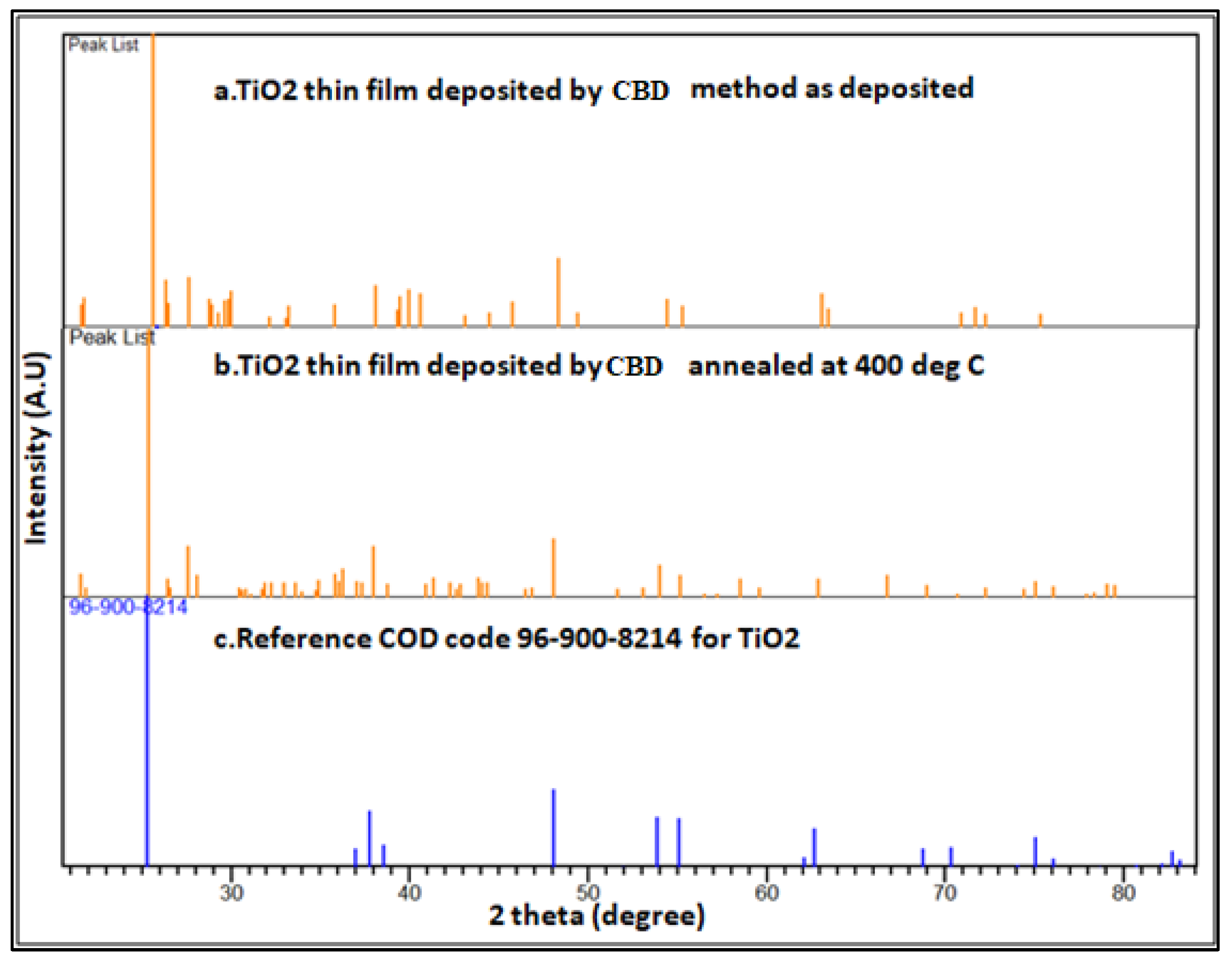
Figure 2 shows a XRD pattern of a chemically deposited thin film of TiO
2, (a) as deposited, (b) annealed at 4000C and (c) standard COD code 96-900-8214 respectively. The elucidation of the crystal structure of the TiO
2 thin film serves as a pivotal milestone in comprehending its properties and facilitates prospective investigations aimed at exploring the interplay between the crystal structure and diverse performance parameters. XRD pattern of annealed thin film has sharp and well-defined peaks at 25.44
0, 27.54
0, 36.24
0, 37.86
0, 48.04
0, 54.02
0,55.16
0, and 62.92
0 corresponding to diffraction from (1, 2, 0), (1, 1, 1), (1,0,3),(1,1,2), (2,0,0), (1,0,5), (2,1,1) and (2,0,4) crystal planes respectively. The concordance observed between the X-ray diffraction (XRD) pattern of the annealed TiO
2 thin film and the reference COD code 96-900-8214 for TiO
2 substantiates compelling evidence of the proficient achievement in synthesizing the intended anatase phase within the thin film. The congruence between the X-ray diffraction (XRD) pattern and the reference COD code 96-900-8214 for TiO
2 indicates that the synthesized TiO
2 thin film exhibits the distinctive lattice parameters and crystallographic orientation inherent to the anatase phase. The crystal structure of the synthesized TiO
2 thin film is tetragonal. This structural confirmation indicates that the synthesized film has the potential for efficient light absorption and charge transport, making it suitable for applications in solar cells and other photoelectrochemical devices. This confirmation reinforces the reliability and reproducibility of the synthesis method employed namely CBD for synthesis and deposition.
The average crystallite size of chemically deposited TiO
2 thin film was computed using the Scherrer formula shown in equation (1) [
20],
Where
λ is the wavelength of X-ray (CuK
α radiation = 0.154 nm),
θ is the Brag diffraction angle and
β is the full width half maximum of the XRD peaks appearing at the different angle
θ. For TiO
2 thin film annealed at 400
0C for 30 minutes, it was calculated and found to be about 27 nm. The measured average crystalline size indicates the presence of distinct nanoscale crystalline domains within the TiO
2 thin film. This refined crystalline structure can potentially enhance the mobility of charge carriers. The diminutive average crystalline size of 27 nm implies a heightened abundance of grain boundaries and interfaces within the TiO
2 thin film.
In the context of thin films, dislocation density refers to the measurable expression of the concentration of dislocations within the crystal lattice structure of the film. Dislocations, characterized as linear defects occurring within the crystal lattice, arise from the misalignment or distortion of atomic planes. While microstrain denotes the quantification of strain or deformation occurring at a localized scale within the crystal lattice structure of the film. It encompasses the assessment of the magnitude pertaining to lattice distortion or atomic plane displacement within a confined region of the thin film. Further the dislocation density (
δ) and micro strain (
ε) of annealed TiO
2 thin film was determined using equations (2) and (3) respectively given below [
21]
Dislocation density and micro strain was calculated as 0.001451/nm2 and 0.149 respectively. The determined dislocation density suggests a low incidence of lattice imperfections and dislocations within the TiO
2 thin film, indicating a high level of structural integrity and crystalline quality. This favorable characteristic can have a positive influence on the film’s properties. The measured micro strain value signifies the existence of localized strain within the TiO
2 thin film, potentially originating from lattice distortions or interfacial lattice mismatch. These distortions have the potential to impact the film’s electronic band structure, resulting in modified optical and electronic properties that are susceptible to strain-induced effects. A reduced magnitude of the dislocation density (δ) signifies a high degree of crystallinity in the TiO
2 thin film [
22].
3.2. Morphological Analysis
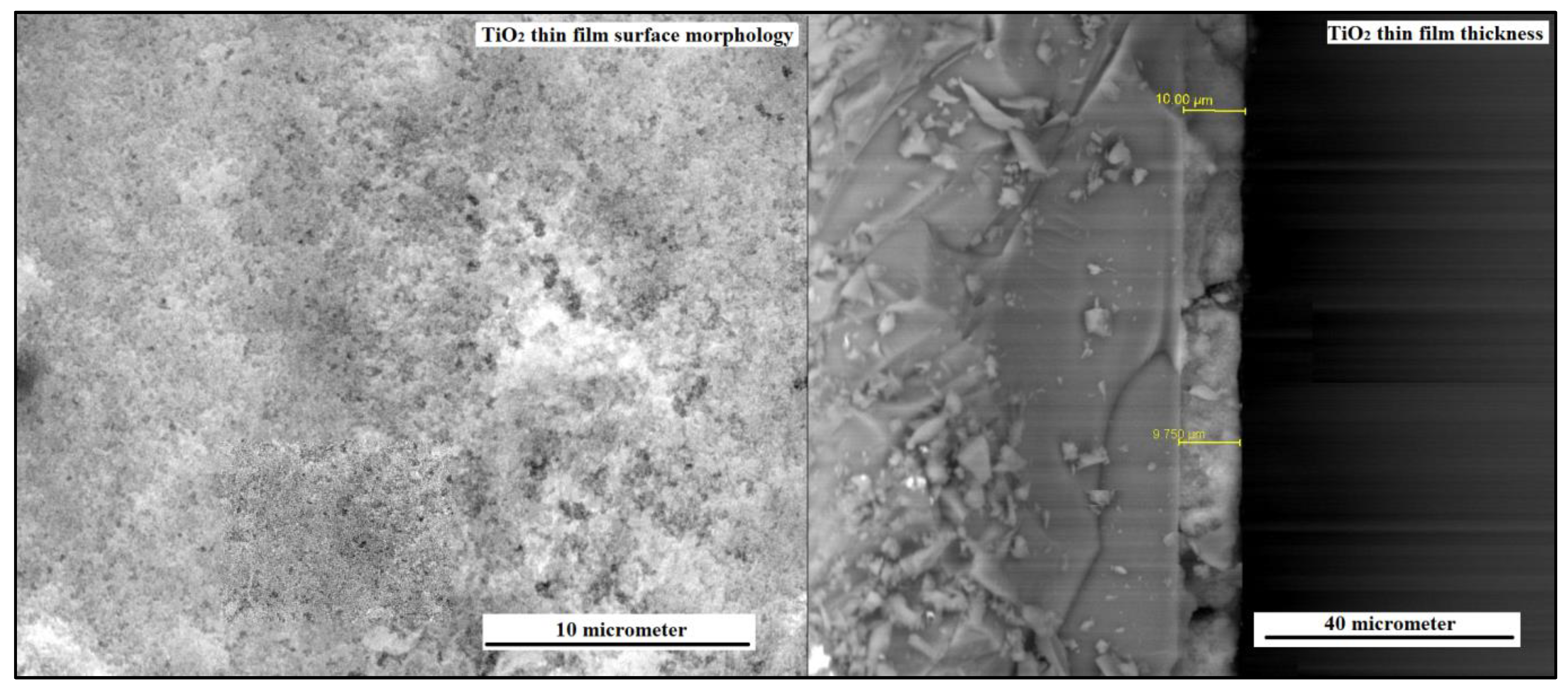
The surface morphological and cross-sectional studies of the TiO
2 were performed using a scanning electron microscope (SEM).
Figure 3 (a) shows the surface morphology of TiO
2 thin film and (b) shows cross-section micrograph of TiO
2 film deposited. The observed spherical morphology of the TiO
2 particles, as visualized in the micrograph, signifies a homogeneous and precisely defined structure throughout the thin film. The lack of cracks or voids within the TiO
2 film signifies an accomplished deposition process and strong adhesion between the film and the substrate. This flawless nature amplifies the film’s mechanical stability, surface uniformity, and overall performance. The interconnection of TiO
2 nanoparticles within the thin film, as evidenced by the micrograph, engenders a mesoporous structure. This interconnected network of nanoparticles yields an expanded surface area and facilitates the diffusion of molecules or ions. The complete coverage of the substrate surface with spherical nano TiO
2 particles, as illustrated in the figure, validates the effectiveness of the synthesis technique in achieving a uniform and continuous coating. The spherical morphology, absence of cracks or voids, and interlinking of TiO
2 nanoparticles exemplify the triumphant fabrication of a top-quality TiO
2 thin film . The thickness of the TiO
2 layer perceived from SEM micrograph is uniform over the entire substrate. The thickness of the TiO
2 layer deposited by CBD technique is very thin and the average thickness computed is 9.875
µm with standard deviation of 0.102
µm. The attainment of a thin TiO
2 layer thickness, as ascertained via the CBD technique, signifies a meticulous and accurate deposition process. The calculated average thickness, coupled with a standard deviation of 0.102µm, showcases the reproducibility and reliability of the CBD method for TiO
2 layer deposition. The slender dimensions of the TiO
2 layer confer benefits in relation to material efficiency and resource optimization, thereby fostering cost-effectiveness and sustainability in the fabrication of TiO
2 thin films.
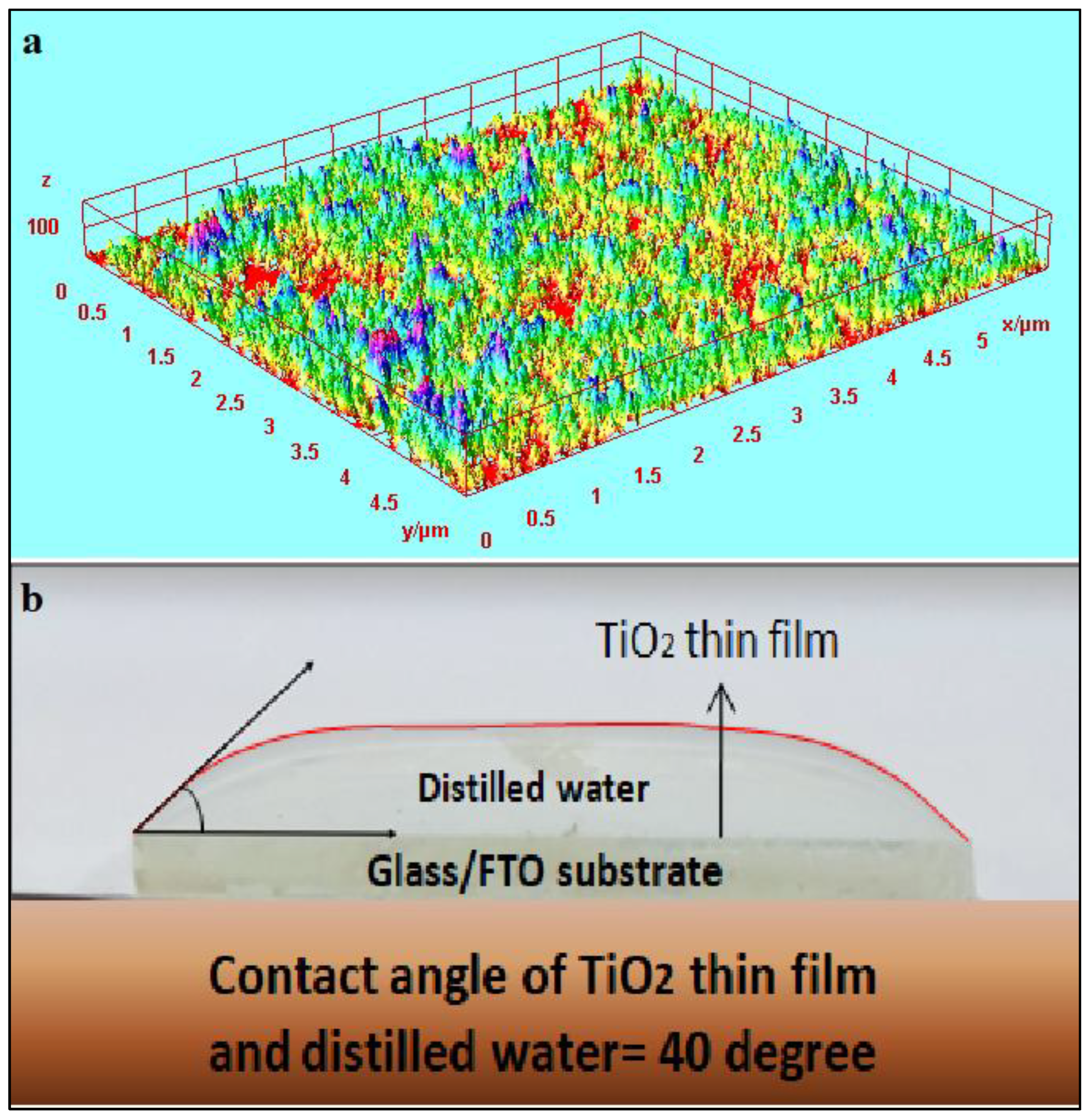
The three-dimensional projection of the TiO
2 thin film, as illustrated in
Figure 4a, offers a visual representation of its structural characteristics and unveils a surface with remarkable permeability. This inherent attribute plays a pivotal role in facilitating efficient material transport and electrolyte penetration, thereby contributing to enhanced device performance, particularly in the context of semiconducting dye-sensitized solar cells (DSSC). The absence of direct vulnerability between the TiO
2 thin film and the glass/FTO substrate signifies the establishment of a resilient and well-bonded interface. This interfacial integrity assumes paramount importance in upholding the film’s structural stability, mitigating risks associated with delamination or detachment, and ensuring the long-term reliability of the device. The presence of mesopores within the TiO
2 thin film fosters an augmented diffusion capacity for the electrolyte, consequently promoting efficient charge transport and diminishing recombination losses. As a result, the overall performance of the device can be elevated. The observed high permeability and mesoporous structure of the TiO
2 thin film underscore its potential as a promising scaffold for accommodating semiconducting dye molecules in dye-sensitized solar cells (DSSC). This characteristic engenders a larger surface area accessible for dye absorption, thereby facilitating superior light harvesting and facilitating efficient charge generation within the device.
The utilization of a high-definition camera for investigating the wettability of the TiO
2 thin film yields valuable insights into the interfacial dynamics between the film surface and water. This analytical approach facilitates the comprehensive characterization of the film’s hydrophilic or hydrophobic behavior, which holds significant implications across diverse applications. The discernible protuberant shape exhibited by the water drop meniscus on the TiO
2-coated glass/FTO substrate signifies a diminished hydrophilic propensity of the surface as depicted in
Figure 4b. Consequently, water manifests reduced affinity towards the TiO
2-coated surface, resulting in attenuated wetting phenomena and slower spreading of water droplets. These inherent characteristics bear advantages in contexts where water repellency or controlled liquid behavior is sought after. Furthermore, the determination of a contact angle measuring 40 degrees for the FTO/TiO
2 film, as depicted in
Figure 4 (b), corroborates the hydrophobic nature of the TiO
2-coated surface. The computed contact angle value signifies a moderately hydrophobic behavior exhibited by the TiO
2 film. The observation of reduced hydrophilic behavior and the derived contact angle measurement pertaining to the TiO
2 coated glass/FTO substrate yield crucial insights into the surface properties of the film, as well as its potential applications. These surface characteristics exert influence over variables such as surface energy, the adhesion of contaminants, and the capability to manipulate liquid droplets, thereby profoundly affecting the operational efficiency and functional attributes of devices or coatings predicated on TiO
2 thin films.
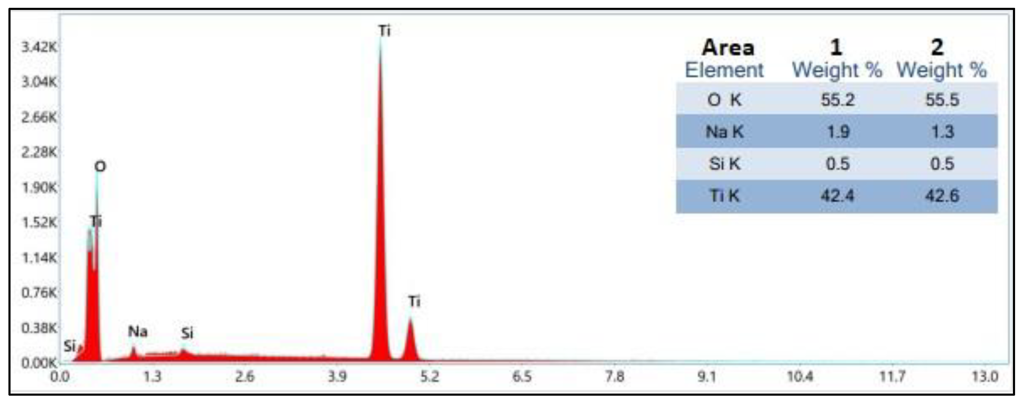
With the view to confirm deposition of TiO
2 thin film energy dispersive X-ray spectroscopy (EDXS) was accomplished. The examination of two distinct regions within the film aimed to evaluate its homogeneity. The EDXS spectra revealed a remarkable similarity in the quantities of titanium (Ti) and oxygen (O) across both investigated areas, indicating a high level of elemental composition consistency throughout the film. The utilization of energy-dispersive X-ray spectroscopy (EDXS) in the elemental analysis, as illustrated in
Figure 5, provided qualitative confirmation of the presence of TiO
2 in the film through the identification of characteristic emission lines for Ti and O. These findings align with the results obtained from X-ray diffraction (XRD) analysis, thereby reinforcing the identification of TiO
2 formation within the film. The uniform quantities of Ti and O observed across the investigated areas suggest a homogeneous composition of the film, which can positively impact its overall quality and performance.
3.4. Optical Properties
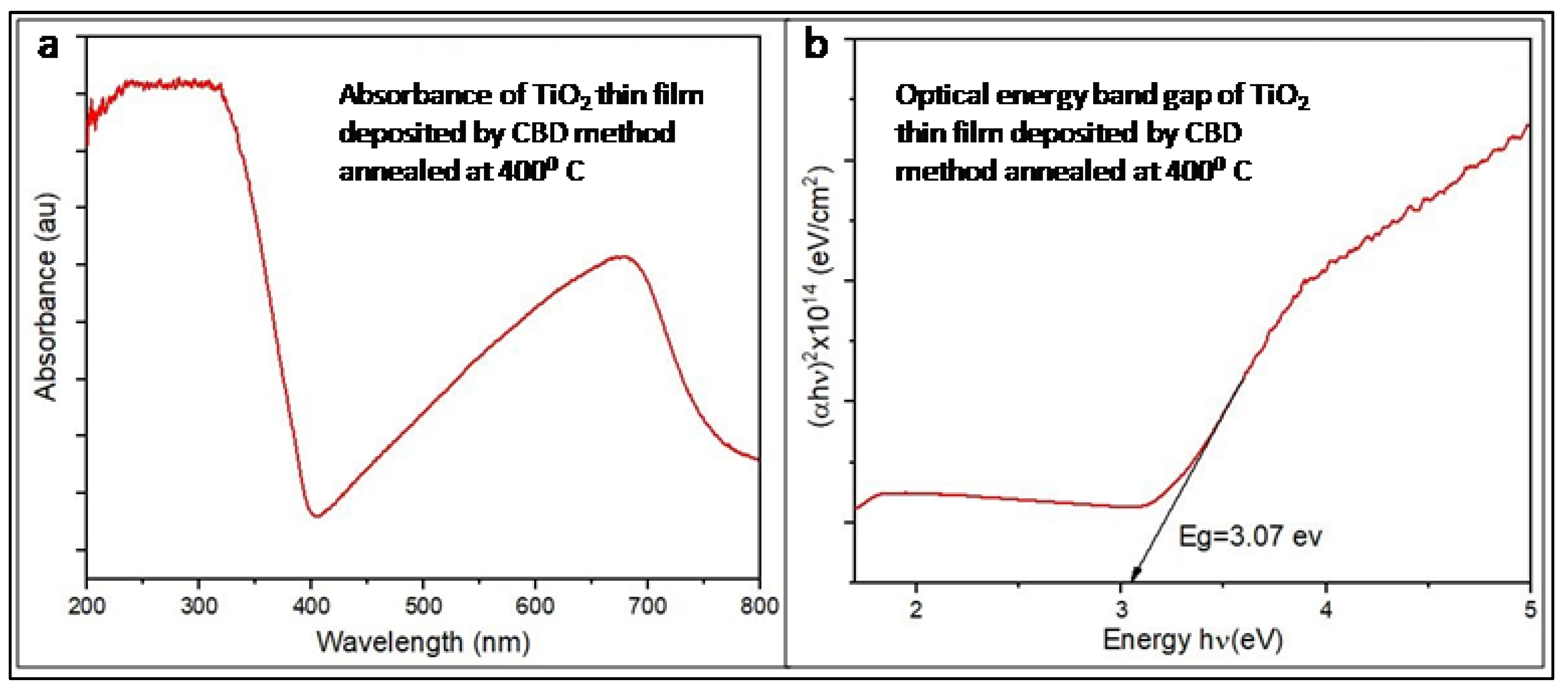
Optical properties play significant role in thin film deposition techniques.
Figure 6a depicts the absorption spectrum of the CBD deposited TiO
2 thin film post-annealing at 400°C. This spectrum showcases the film’s response to incident light across a broad range of wavelengths, offering valuable insights into its optical properties and potential applications. The analysis reveals a prominent maximum absorption peak at approximately 350 nm, indicating the wavelength region where the film displays the highest absorption of incident photons. Accurate knowledge of this peak absorption wavelength holds significance in optimizing the film’s performance in fields like photocatalysis and photovoltaics. The absorption spectrum exhibits distinctive absorption trends at different wavelengths. The range from 350 to 400 nm shows a sharp decline in absorbance, succeeded by a gradual increase as the incident photon wavelength extends until 700 nm. Another maximum absorption peak emerges around 700 nm, while absorbance diminishes beyond 700 nm until 800 nm. These absorption characteristics provide insights into the film’s interaction with incident light and its potential for light absorption and energy conversion. The relationship between absorbance and film thickness is directly proportional, indicating that a thicker film will exhibit higher optical absorbance. Understanding this correlation is crucial for tailoring the film’s optical properties and optimizing its performance in light-harvesting applications. Additionally, an direct relationship exists between optical absorbance and thin film thickness. Higher depositional time during the CBD method lead to increased film thickness, resulting in higher optical absorbance [
23].
Figure 6b depicts the optical energy band gap graphs of the TiO
2 thin film, offering crucial information about its energy levels and its potential for light absorption and electronic transitions. Analyzing the optical energy band gap provides insights into the film’s optical properties and its suitability for diverse optoelectronic applications. To calculate the optical energy band gap of the chemically deposited TiO
2 photo electrode, the (hν) versus (αhν)
2 graph was utilized. By examining the relationship between the incident photon energy (hν) and the square of the absorption coefficient (αhν), the value of the optical energy band gap was determined. In this instance, the calculated value is approximately 3.07 eV, as indicated in
Figure 6b.The determined optical energy band gap of around 3.07 eV yields significant insights into the film’s electronic structure and its ability to absorb light in the visible spectrum. Films with wider band gaps generally exhibit greater transparency to visible light, while narrower band gaps allow for absorption of a broader range of photons. The optical energy band gap determination of 3.07 eV implies that the TiO
2 thin film possesses the capability to undergo electronic transitions upon absorption of photons with energies corresponding to visible light wavelengths. This characteristic holds significant implications for harnessing light energy and facilitating processes such as electron excitation, charge separation, and photocurrent generation. Consequently, the film exhibits suitability for a wide range of photoelectronic applications.
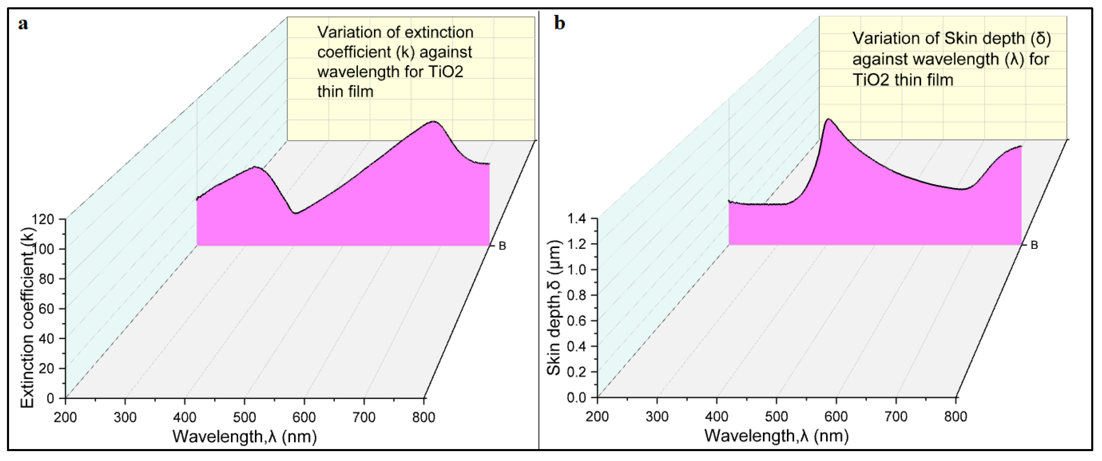
The extinction coefficient (k) of a thin film quantifies how much light passing through it is either absorbed or scattered, providing a measure of the film’s capability in attenuating light [
24]. The skin depth (δ) of a thin film is the distance over which an electromagnetic wave passing through the film is reduced to around 37% (1/e) of its original amplitude [
25]. The
Table 1 show values of extinction coefficient (k) and skin depth (δ) of TiO
2 thin film calculated using UV-visible spectroscopy data.
Figure 7a,b show the variation of extinction coefficient (k) and skin depth (δ) with wavelength of light for TiO
2 thin film respectively. The analysis of the extinction coefficient of the TiO
2 thin film provides valuable insights into its light absorption properties. The film exhibits a maximum extinction coefficient at approximately 700 nm, indicating its highest absorption capacity within this specific wavelength range. Conversely, the film demonstrates a minimum extinction coefficient at 400 nm, suggesting minimal absorption at this particular wavelength. The extinction coefficient serves as a quantitative measure of the film’s ability to attenuate incident light, and these findings highlight the wavelength-dependent nature of its light absorption behavior. The observed variation of the extinction coefficient with respect to wavelength reveals a consistent increase in light absorption as the wavelength increases from 400 to 700 nm. This implies that the TiO
2 thin film progressively absorbs more light within this range, indicating its wavelength-dependent light absorption characteristics. These results provide important insights into the film’s optical properties and its potential for applications requiring efficient light absorption, such as light-harvesting systems.
Furthermore, the relationship between the extinction coefficient and the skin depth, as depicted in
Figure 7, demonstrates an intriguing complementarity with changes in the wavelength of incident light for the TiO
2 thin film deposited via the CBD technique. At 400 nm, the film exhibits the maximum skin depth, indicating the greatest depth of light penetration into the film before significant attenuation occurs. However, as the wavelength increases beyond 400 nm up to 700 nm, the skin depth decreases, indicating reduced light penetration and increased absorption within a shallower region of the film. Beyond 700 nm, the skin depth starts to increase again. This relationship between the extinction coefficient and the skin depth highlights the interdependence of these optical parameters and their reliance on the wavelength of incident light.
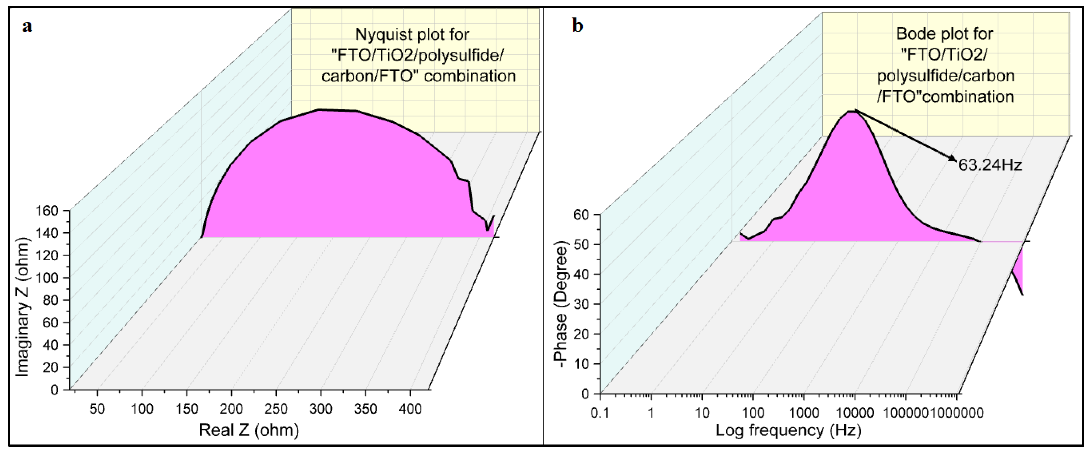
3.5. Electrochemical Impedance Spectroscopy
Figure 8a indicates electrochemical impedance spectroscopy plot for FTO/TiO
2 photoelectrode/polysulfide electrolyte/carbon electrode/FTO combination under the dark condition with magnitude of modulation signal with 5mV ranging from 1 MHz to 0.1 Hz. The EIS technique provides valuable insights into the electrochemical behavior of the system under investigation. The Nyquist plot, which graphically represents the impedance response by plotting the real part of impedance on the X-axis and the imaginary part on the Y-axis, reveals important information about the system’s charge transfer processes. In the obtained Nyquist plot, a single perfect semicircle is observed. This semicircle signifies a well-defined charge transfer process taking place at the carbon electrode-polysulfide electrolyte boundary. The size of the semicircle at higher frequencies corresponds to the magnitude of the charge transfer resistance and recombination resistance at this interface. A larger semicircle indicates higher resistance, which implies slower charge transfer and increased recombination processes. The presence of a single semicircle in the Nyquist plot suggests a relatively simple electrochemical behavior, with a dominant charge transfer mechanism operating at the electrode-electrolyte interface.
Figure 8b represents Bode plot for cell fabricated from FTO/TiO
2 photo electrode/polysulfide electrolyte/carbon electrode/FTO combination without any semiconducting dye molecule. The absence of a semiconducting dye molecule allows us to examine the intrinsic characteristics of the TiO
2 thin film and its interface with the polysulfide electrolyte in terms of electron lifetime. The electron lifetime serves as an indicator of the recombination rate and the efficacy of charge carrier separation and collection within the fabricated device. A longer electron lifetime signifies a reduced recombination rate, indicating enhanced charge carrier retention and superior charge transfer across the TiO
2 thin film. Conversely, a shorter electron lifetime suggests a higher recombination rate and a less efficient charge transport process. Analyzing the electron lifetime in the absence of a semiconducting dye molecule provides a foundational benchmark for evaluating the performance of the TiO
2 thin film device. This information aids in assessing the device’s efficiency and identifying potential areas for improvement in terms of charge carrier dynamics and overall functionality. The peak of the plot can be used to find the electron lifetime as per the equation (4) [
26].
where
τ is electron lifetime and f is maximum frequency from Bode plot.
The electron lifetime calculated from Bode plot is 2.51 ms. A longer electron lifetime of 2.51 ms indicates a lower recombination rate, reflecting efficient charge carrier dissociation and improved charge transfer kinetics within the TiO2 thin film. This prolonged electron lifetime signifies an advantageous condition for charge carrier preservation, facilitating efficient charge transport and collection within the device.
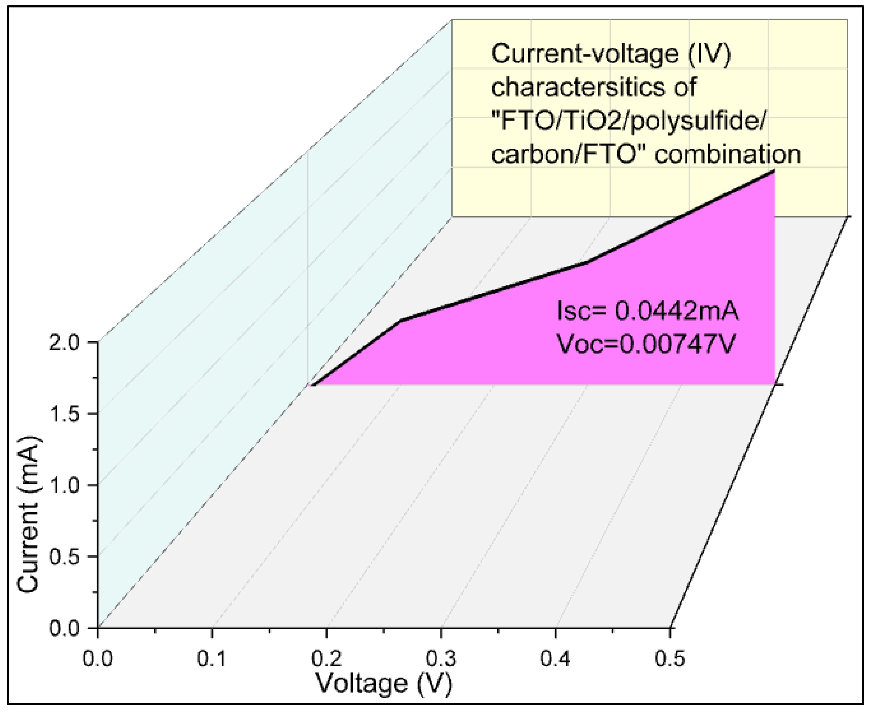
3.6. Photoelectrochemical Analysis
Figure 9 shows photoelectrochemical analysis using current-voltage characteristics of FTO/TiO
2 photoelectrode/ polysulfide electrolyte/carbon electrode/FTO device. The obtained photoelectrochemical parameters are enlisted in
Table 2. The current-voltage (IV) characteristics displayed a current density of 0.0884 mA/cm², indicating the magnitude of current flowing through the device under the applied voltage. The absence of semiconducting dye molecules in the fabricated device has led to a deficiency in light absorption enhancement, resulting in a lack of efficiency and fill factor. In semiconductor or dye-sensitized solar cells, the presence of semiconductor or dye molecules surrounding the TiO
2 molecules plays a pivotal role in augmenting light absorption. These molecules aid in the generation of free electrons for conduction, thereby improving device performance. However, the absence of such dye molecules prevents efficient conversion of incident light into electrical energy, leading to zero efficiency and fill factor. This emphasizes the importance of incorporating semiconducting dye molecules into the device architecture to enhance its overall performance and efficiency.
4. Discussion
This study presents a facile synthesis and deposition of a TiO2 thin film by CBD, demonstrating a combination of structural, morphological, optical, and photoelectrochemical properties that hold significant promise for optoelectronic applications. The successful synthesis of a highly crystalline anatase TiO2 thin film with a nanoscale crystallite size (27 nm) is a key achievement. This nanoscale dimension is crucial for enhancing the surface area and promoting efficient charge transport, both vital for applications like photocatalysis and solar energy conversion. The observed mesoporous and uniform morphology, as revealed by SEM, further contributes to the high surface area and facilitates interaction with target molecules or electrolytes. The measured film thickness of 9.875 µm, while significant, indicates a robust film suitable for practical applications. The contact angle of 40 degrees suggests a moderately hydrophilic surface, which can be advantageous in certain applications, such as biosensing, where controlled interaction with aqueous solutions is desired. While not super hydrophilic, this value offers a balance between surface wetting and potential fouling.
The optical properties of the TiO2 film, particularly the strong absorption across the UV, near-IR, and IR regions, are noteworthy. This broad absorption spectrum expands the potential applications beyond traditional UV-only photocatalysis, suggesting its suitability for devices operating in a wider range of the electromagnetic spectrum. The calculated optical band gap of 3.07 eV is consistent with reported values for anatase TiO2 and confirms its semiconducting nature. The observed correlation between the extinction coefficient and skin depth provides valuable insights into the light interaction mechanisms within the film, crucial for optimizing device performance.
The photoelectrochemical analysis, even without dye sensitization, demonstrates a baseline current density of 0.0884 mA/cm² with the polysulfide electrolyte. This intrinsic photocurrent generation indicates the potential of the TiO2 film for direct charge transfer and lays the groundwork for future sensitization studies. This baseline performance is crucial for evaluating the effectiveness of subsequent dye sensitization efforts. The fact that a measurable current was observed is significant given that the TiO2 was not doped or otherwise modified to enhance conductivity.
This study has some limitations. The photoelectrochemical performance was evaluated using a polysulfide electrolyte, and the performance with other electrolytes relevant to specific applications (e.g., those used in dye-sensitized solar cells) was not explored. Furthermore, a detailed investigation of the photocatalytic activity of the TiO2 thin film was not conducted, although the structural and morphological characteristics suggest its potential in this area. The long-term stability and performance of the TiO2 film under operating conditions were also not assessed, which is an important factor for practical applications. Finally, the study focuses on a relatively simple synthesis and deposition method. More advanced techniques might yield even higher performance TiO2 films.
5. Conclusions
This study provides a comprehensive characterization of TiO2 thin films synthesized via a CBD method, highlighting their potential for various optoelectronic applications. The combination of structural, morphological, optical, and photoelectrochemical characterization provides a strong foundation for future research. The results suggest that TiO2 thin films are indeed promising for solar cell, photocatalytic, biosensing, and other optoelectronic applications. Future work will focus on sensitizing the TiO2 film with different semiconducting dye molecules to enhance the absorption of solar radiation and improve the overall device performance. Exploring different electrolyte systems and investigating the photocatalytic activity are also planned. These investigations will contribute to a deeper understanding of the material’s properties and pave the way for its practical implementation in advanced technological applications.
Funding
“There are no sources of funding to declare.”
Author contributions
Conceptualization: Sachin Padwal, Dr Rahul Wagh, Shaurya Padwal, Dr Rajendra Patil; Methodology: Sachin Padwal, Shaurya Padwal; Formal analysis and investigation: Sachin Padwal, Dr Rahul Wagh; Writing - original draft preparation: Sachin Padwal; Writing - review and editing: Sachin Padwal, Shaurya Padwal; Funding acquisition: Not applicable; Resources: Sachin Padwal, Shaurya Padwal; Supervision: Dr Rahul Wagh, Shaurya Padwal, Dr Rajendra Patil
Institutional Review Board Statement
“Not applicable.”
Informed Consent Statement
“Not applicable.”
Data Availability Statement
The data that support the findings of this study are available from the corresponding author, upon reasonable request.
Sample Availability
“The author(s) declare that no physical samples were used in this study.”
Acknowledgments
The authors sincerely acknowledge the Kaviyatri Bahinabai Chaudhari North Maharashtra University Jalgaon, Department of Physics PSGVP Mandal’s Arts, Commerce & Science College Shahada, Nandurbar, Advanced Physics Lab-Department of Physics, Savitribai Phule University Pune, Baburaoji Gholap Science College Pune and Icon Analytical New Mumbai for providing characterization facilities.
Conflict of Interest
“The author(s) declare no conflict of interest.”
References
- Okada, M. “Fabrication of multifunctional coating which combines low-e property and visible-light-responsive photocatalytic activity” Thin Solid Films, 442(1-2), 217-221, (2003).
- D’Amico, N. R., Cantele, G., & Ninno, D. “First principles calculations of the band offset at SrTiO3−TiO2 interfaces” Applied Physics Letters, 101(14), 141606, (2012).
- Manno, D., Micocci, G., Rella, R., Serra, A., Taurino, A., & Tepore, A. “Titanium oxide thin films for NH3 monitoring: Structural and physical characterizations”. Journal of Applied Physics, 82(1), 54–59, (1997). [CrossRef]
- Wang, Z., & Hu, X. “Fabrication and electrochromic properties of spin-coated TiO2 thin films from peroxo-polytitanic acid”. Thin Solid Films, 352(1-2), 62-65, (1999). [CrossRef]
- Liu, J.-X., Yang, D.-Z., Shi, F., & Cai, Y.-J.“Sol–gel deposited TiO2 film on NiTi surgical alloy for biocompatibility improvement”. Thin Solid Films, 429(1-2), 225–230, (2003). [CrossRef]
- Bendavid, A., Martin, P. J., & Takikawa,H. “Deposition and modification of titanium dioxide thin films by filtered arc deposition”. Thin Solid Films, 360(1-2), 241–249, (2000). [CrossRef]
- Williams, L. M., D W Hess “Structural properties of titanium dioxide films deposited in an rf glow dicharge”, J. Vac. Sci. Technol. A, 1, 1810-1819, (1983).
- Suzuki, S., Ohsaki, H. O. H., & Ando, E. A. E. “Materialistic difference in macroscopic friction coefficients of sputtered metal oxide thin films deposited on glass”. Japanese journal of Applied Physics, 35(3R), 1862, (1996). [CrossRef]
- Elfanaoui, A., Ihlal, A., Taleb, A., Boulkaddat, L., Elhamri, E. and Meddah, M. et al “The synthesis of TiO2 thin film by chemical bath deposition (CBD) method”. Moroccan Journal of Condensed Matter, 13(3), (2011).
- Aarik, J., Aidla, A., Kiisler, A. A., Uustare, T., & Sammelselg, V. “Effect of crystal structure on optical properties of TiO2 films grown by atomic layer deposition.” Thin Solid Films, 305(1-2), 270-273, (1997). [CrossRef]
- Fujii, T., Sakata, N., Takada, J., Miura, Y., Daitoh, Y., & Takano, M. “Characteristics of titanium oxide films deposited by an activated reactive evaporation method”. Journal of materials research, 9(6), 1468-1473, (1994). [CrossRef]
- Amor, S. B., Baud, G., Besse, J. P., & Jacquet, M. “Elaboration and characterization of titania coatings”. Thin Solid Films, 293(1-2), 163-169, (1997). [CrossRef]
- Okimura, K. O. K., Shibata, A. S. A., Maeda, N. M. N., Tachibana, K. T. K., Noguchi, Y. N. Y., & Tsuchida, K. T. K. “Preparation of rutile TiO2 films by RF magnetron sputtering”. Japanese journal of applied physics, 34(9R), 4950, (1995).
- Gilo, M., & Croitoru, N.“Properties of TiO2 films prepared by ion-assisted deposition using a gridless end-Hall ion source”. Thin Solid Films, 283(1-2), 84-89, (1996). [CrossRef]
- Mosaddeq-ur-Rahman, M., Yu, G., Krishna, K. M., Soga, T., Watanabe, J., Jimbo, T., & Umeno, M. “Determination of optical constants of solgel-derived inhomogeneous TiO2 thin films by spectroscopic ellipsometry and transmission spectroscopy”. Applied optics, 37(4), 691-697, (1998). [CrossRef]
- O’regan, B., & Grätzel, M. “A low-cost, high-efficiency solar cell based on dye-sensitized colloidal TiO2 films”. Nature, 353(6346), 737-740, (1991).
- Lottiaux, M., Boulesteix, C., Nihoul, G., Varnier, F., Flory, F., Galindo, R., & Pelletier, E. “ Morphology and structure of TiO2 thin layers vs. thickness and substrate temperature”.Thin solid films, 170(1), 107-126, (1989).
- Tian, H. Y., Luo, W. G., Ding, A. L., Choi, J., Lee, C., & No, K. “ Influences of annealing temperature on the optical and structural properties of (Ba, Sr) TiO3 thin films derived from sol–gel technique”. Thin Solid Films, 408(1-2), 200-205, (2002).
- Mathews, N. R., Morales, E. R., Cortés-Jacome, M. A., & Antonio, J. T. “TiO2 thin films–Influence of annealing temperature on structural, optical and photocatalytic properties”. Solar energy, 83(9), 1499-1508, (2009).
- B Cullity, Elements of X-ray diffraction, USA Addision-Wisley Publishing company Inc.Moris Cohen 2nd edition, p 262 (1978).
- Kaltenhauser, V., Rath, T., Haas, W., Torvisco, A., Müller, S. K. and Friedel, B. et al “Bismuth sulphide–polymer nanocomposites from a highly soluble bismuth xanthate precursor”. Journal of Materials Chemistry C, 1(47), 7825-7832, (2013).
- Islam, M. A., Hossain, M. S., Aliyu, M. M., Chelvanathan, P., Huda, Q. and Karim, M. R., et al ”Comparison of structural and optical properties of CdS thin films grown by CSVT, CBD and sputtering techniques”. Energy Procedia, 33, 203-213, (2013).
- Dundar, I., Mere, A., Mikli, V., Krunks, M., & Oja Acik, I.“Thickness Effect on Photocatalytic Activity of TiO2 Thin Films Fabricated by Ultrasonic Spray Pyrolysis”. Catalysts, 10(9), 1058 (2020). [CrossRef]
- Rathod, P., Nemade, K., & Waghule, S. “Study of Structure and Optical for Chemically Synthesized Titanium Dioxide Nanoparticles” International Journal of Chemical and Physical Sciences, 4, 491-495, (2015).
- El-Haija, A. A., & Wishah, K. A. “Basic optical properties: effective optical constants, skin depth, absorption coefficients and optical conductivity of an ultrathin Ag-SiO superlattice identity period”. Optica Applicata, 31(4), 739-749, (2001).
- Majumder, S., Baviskar, P. K., & Sankapal, B. R. “Light-induced electrochemical performance of 3D-CdS nanonetwork: effect of annealing”. Electrochimica Acta, 222, 100-107, (2016). [CrossRef]
|
Disclaimer/Publisher’s Note: The statements, opinions and data contained in all publications are solely those of the individual author(s) and contributor(s) and not of MDPI and/or the editor(s). MDPI and/or the editor(s) disclaim responsibility for any injury to people or property resulting from any ideas, methods, instructions or products referred to in the content. |
© 2025 by the authors. Licensee MDPI, Basel, Switzerland. This article is an open access article distributed under the terms and conditions of the Creative Commons Attribution (CC BY) license (https://creativecommons.org/licenses/by/4.0/).