
Submitted:
16 April 2024
Posted:
18 April 2024
You are already at the latest version
Abstract
The undoped and tungsten (W)-doped vanadium dioxide (VO2) thin films were prepared by electron beam evaporation associated with ion-beam assisted deposition (IAD). The influence of different W-doped contents (3%-5%) on the optical, electrical, structural, and thermos-mechanical properties of VO2 thin films was investigated experimentally. Spectral transmittance results showed that with the increase of W-doped contents, the transmittance in the visible light range (400-750 nm) decreases from 60.2% to 53.9%, and the transmittance in the infrared wavelength range (2.5 μm to 5.5 μm) drops from 55.8% to 15.4%. As the W-doped content increases, the residual stress in the VO2 thin film decreases from -0.276 GPa to -0.238 GPa, but the surface roughness increases. For temperature-dependent spectroscopic measurements, heating the VO2 thin films from 30°C to 100°C showed the most significant change in transmittance for the 5% W-doped VO2 thin film. When the heating temperature exceeds 55°C, the optical transmittance drops significantly, and the visible light transmittance drops by about 11%. Finally, X-ray Diffraction (XRD) and scanning electron microscope (SEM) were used to evaluate the microstructure characteristics of VO2 thin films.
Keywords:
Vanadium dioxide
; thin film
; electron beam evaporation
; ion-assisted deposition
1. Introduction
Vanadium oxide is a typical thermochromic material exhibiting a metal-insulator transition (MIT) near room temperature. Unprecedented modulation of IR transmission is achieved by the addition of up-conversion nanoparticles [1]. Vanadium can exist in various oxidation states, forming different oxides, and obtaining high-purity vanadium oxide presents challenges, requiring optimal temperature and pressure conditions. Vanadium dioxide (VO2) has garnered widespread attention due to its unique insulator-to-metal phase transition characteristics. As the temperature changes, VO2 undergoes a reversible transition between the insulating and metallic states, leading to significant changes in its electrical and optical properties. For undoped VO2, the phase transition temperature is typically 68°C, limiting its application in various energy-saving-related uses that require room temperature as the control threshold [2]. VO2 enables the transition from insulator to metal (IMT) and the transition from a monoclinic (M1) to a rutile structure (R) at around 68℃. Monoclinic VO2 (VO2(M)) is stable at temperatures below 68°C and exhibits semiconductor properties. Rutile VO2 is stable above 68°C and has metallic properties that cause infrared reflection [3]. Different metallic vanadium thin film surface roughness and particle size have different oxidation time to fabricate VO2 thin film. Phase transition properties and crystallization of VO2 thin film can be deeply affected by oxidation time [4]. Thus, VO2 is a promising thermochromic material used in smart windows that can control infrared transmittance during temperature changes.
In recent years, VO2 has received widespread attention due to its significant reversible changes in electrical and optical properties, especially near 68°C, making it more suitable for practical technical applications. However, the transition temperature (Tt) of VO2 is still too high for energy applications related to room temperature [5]. In most cases, it is necessary to lower Tt to approach ambient temperatures to maximize the benefits from variable solar energy influx, and efforts have been made to reduce Tt through the doping of metal ions. Dou et al. [6] found that tungsten is an effective method for lowering the phase transition temperature. W-doped VO2 films not only lower phase transition temperature and narrow hysteresis loops width, but also enhance cycle stability. For W-doped VO2, the decrease in the transition temperature is attributed to the formation of V3+-W6+ pairs through the crystallization of VO2 into a monoclinic structure, resulting in a weakening of the bonding strength between V ions. The formation of these V3+-W6+ pairs occurs as two electrons from the d-orbital of tungsten move to adjacent V ions for charge compensation. Thus, with an increase in the W6+ content in the lattice, the V4+-V4+ bond weakens, leading to semiconductor phase instability and a decrease in the transition temperature. The synthesized W-doped VO2 thin film presents Tt=47°C [7]. Takami et al. [8] experimentally found that tungsten doping increases carrier concentration, altering the Coulomb repulsion energy and stabilizing the metallic state of the thin film. However, the growth of tungsten-doped vanadium dioxide (W:VO2) also presents challenges, such as the instability of the ability to lower the phase transition temperature of VO2 through tungsten doping, with significant variations in results based on different preparation techniques, especially in achieving precise tungsten doping over large surface areas. Haining [9] et al. successfully prepared a thin film that lowered the phase transition temperature of vanadium dioxide by changing the doping ratio of tungsten. When the doping amount of tungsten is 1.70%, the phase transition temperature decreases from 67°C to 43.2°C. It is worth mentioning that the infrared characteristics of tungsten-doped vanadium dioxide nanoparticles were studied in the MWIR (3-5 μm) and LWIR (8-14 μm) infrared bands for the first time. They showed an excellent solar light modulation rate (ΔTsol) is 23%, and is accompanied by the modulation of emissivity as Δε = 0.17 and Δε = 0.28, respectively. These results further promote the application of the development of smart windows. Ye and Zhou [10] proposed that when tungsten is successfully doped into the vanadium dioxide lattice, the tungsten-doped vanadium dioxide will exhibit a rod-like morphology, and discussed the phase transition temperature and annealing temperature. The phase transition temperature of vanadium dioxide can be adjusted by changing the doping concentration of tungsten. When the doping concentration is 1.58 mol %, the phase transition temperature can be reduced from the initial 69.5°C to 37.8°C, indicating that tungsten doping vanadium dioxide can exhibit outstanding thermochromic properties.
This study aims to investigate the influence of W-doped contents on the optical, electrical, structural and thermo-mechanical properties of the thermochromic vanadium dioxide thin films. Understanding the characteristics of VO2 thin films from various instrument measurements can help improve the film’s durability for applications in smart windows, optoelectronic switches, and intelligent heat dissipation devices.
2. Materials and Methods
2.1. Preparation of Tungsten-Doped Vanadium Dioxide Thin Films with Different Contents
Electron beam evaporation is a technique capable of achieving the growth of thin films over large surface areas. The evaporation chambers are typically configured to accommodate multiple substrates simultaneously, thus demonstrating exceptional production efficiency. This method offers advantages such as reduced processing time and ease of maintenance, rendering it a prevalent choice in industrial applications for producing optical coatings, transparent conductive films, and related products [11,12]. This study utilized the SHOWA ion-assisted electron beam deposition system to deposit tungsten-doped vanadium oxide thin films with different doping contents. Tungsten doping concentrations of 0%, 3%, 4%, and 5% were used in the process. B270 and H-K9L glass substrates with a diameter of 25 mm were used, and the substrate heating temperature was maintained at 240°C throughout the process. The electron beam generated by the electron gun bombarded the material and deposited it onto the substrate. The vacuum system consists of an oil rotary pump (RP) and a mechanical booster pump. A diffusion pump is used for the fine pumping operation, a helium cold trap (helium cold trap) captures water vapor in the form of helium condensation in an air compressor to help improve the efficiency of the vacuuming rate. The VO2 thin films were prepared by electron-beam evaporation with ion beam-assisted deposition. The vacuum chamber was evacuated to a base pressure of less than 2.7×10⁻⁴ Pa. Thin films were deposited on B270 and H-K9Lglass substrates (25 mm in diameter), and silicon wafer substrates. These coating substrates were cleaned by ultrasonication. Argon and oxygen gases (99.999% purity) were used in the coating process. During the thin film deposition, the maximum output power of the electron gun was 10 kW, the voltage was 10 kV, and the current was 1 A. The anode current of the ion source for ion-assisted deposition was 0.5-10A, the anode voltage was 80-300V, and the ion energy was 50-200 eV. The film thickness monitoring used quartz monitoring and optical monitoring methods. The quartz monitoring device adopted a 5 MHz quartz crystal oscillator; the optical monitoring used a spectrometer with a wavelength range of 360 nm to 1000 nm and reflected the change in reflectance when the film was deposited on the glass substrates. The extreme points of reflectivity were used to stop the process. In this work, we set the deposition thickness of all VO2 thin films to 100 nm. The vacuum value of the coating process was below 6 ×10⁻⁴ Pa. The electron beam power during evaporation of VO2 was 7.5 kW. The working pressure is 3.0×10⁻² Pa. The deposition rate was 0.1 nm/s. The oxygen gas injected during the VO2 layer deposition was 20 sccm. For the ion-assisted deposition, the argon flow rate was 16 sccm for the VO2 layer. The anode voltage and anode current were 130 V and 2 A for thin film deposition. During the VO2 coating process, the temperature of the different substrates was heated to 280 ˚C.
2.2. Characterization Measurement of Tungsten-Doped Vanadium Dioxide Thin Films
To understand the post-deposition characteristics of the VO2 thin films, this research employed the Shimadzu UV-2600i UV-Vis-NIR spectrophotometer and a temperature-controlled heating stage. Spectral measurements were performed by two instruments: one is a UV-Vis-NIR spectrophotometer covering the wavelength range from 200 nm to 900 nm, and transmittance measured after heating. The other is Fourier transform infrared spectroscopy (FTIR), which measures transmittance in the infrared range of 2.5 μm to 5.5 μm. A homemade Twyman-Green interferometer and Linnik microscopic interferometer were utilized to measure the residual stress and root-mean-square surface roughness of the VO2 thin films [13,14]. Additionally, Raman spectroscopy analysis was employed to examine the crystal structure of the films.
Different instruments are used to measure the optical transmittance, resistivity, residual stress, surface roughness and microstructure characteristics of the VO2 thin films after the coating process. The optical transmittance was measured by a Shimadzu UV-2600i spectrometer with a resolution of 0.1 nm and a wavelength range of 200 nm to 1000 nm. In the residual film stress measurement, a homemade Twyman-Green interferometer was used as the hardware architecture to measure the residual film stress. In a previous publication [13], a semiconductor laser beam is passed through a micro-objective and a pinhole which acts as a spatial filter to form a point source. This beam propagates through a collimating lens to form a plane wavefront. The wavefront is divided in amplitude by a beam splitter. The reflected and transmitted beams travel to a reference mirror (flatness of λ/20) and the glass substrate. The tested glass substrate is mounted on a three-axis platform to generate the spatial carrier frequency and forms interference fringes. After being reflected by both the reference mirror and the substrate, the beams are recombined by the beam splitter and travel toward a digital CMOS camera. The camera has a resolution of 1920 × 1200 pixels. The interference pattern can be seen on the monitor attached to the CMOS camera. The interferogram is recorded by a personal computer equipped with a self-developed MATLAB film stress analysis program.
A homemade Linnik microscopic interferometer [14] was used to measure the surface roughness of the thin film. A He-Ne laser with a wavelength of 632.8 nm is used as the light source. When the laser light passes through the spatial filter and the collimating lens, a parallel light is formed. A beam splitter divides the incident light into two parallel light beams. One beam strikes the reference mirror surface, and the other beam hits the surface of the tested sample after passing through the microscope objective lens. When the two beams are reflected separately and overlapped by the beam splitter, they are on the imaging plane. The interference fringes are captured by a high-resolution CCD camera, and then interferograms are analyzed by the self-developed MATLAB program. The analytical program mainly uses the fast Fourier transform method to obtain the change in height difference of the thin film surface. Secondly, a digital Gaussian filter is used to define the signal cut-off wavelength to separate the high-frequency roughness signal from the low-frequency surface profile. Finally, the 3D surface profile of the thin film can be reconstructed, and the surface roughness parameter values can be calculated through numerical analysis [15]. The electrical property of the VO2 thin film was tested with the standard four point probe method. In addition, X-ray diffraction (XRD) is a powerful analytical method for characterizing materials and understanding their structural features. The microstructure of VO2 thin films was observed by Hitachi S-4800 field emission scanning electron microscope (FE-SEM).
3. Results and Discussion
3.1. Optical Properties of Undoped VO2 and W-Doped VO2 Thin Films
3.1.1. Transmission Spectral Characteristics of Undoped VO2 and W-Doped VO2 Thin Films
Optical spectral characteristics of W-doped VO2 thin films were measured by the Shimadzu UV-2600i UV-Visible spectrophotometer. From the UV-visible light measurement results, the average transmittance of B270 glass substrate coated with W-doped VO2 thin films with different contents of 3%, 4%, 5%, and undoped VO2 thin film was determined in the wavelength range of 300-900 nm, as shown in Figure 1. The visible light transmittances of 3%, 4%, 5%, and undoped VO2 thin films are 60.2%, 56.3%, 53.9%, and 67.2%, respectively. Tungsten doping may influence the crystal structure of vanadium dioxide, such as grain size and grain boundary characteristics. As the doping concentration increases, the grain size of the VO2 thin film gradually increases. These changes may increase light scattering and reflection, thereby affecting optical transmittance.
3.1.2. Infrared Transmittance Spectra of Undoped VO2 and W-Doped VO2 Thin Films
Fourier transform infrared spectroscopy (FTIR) is used to determine the infrared transmittance. The transmittance spectra of VO2 thin films are obtained by varying the tungsten dopant concentration in the wavelength range of 2.5 μm to 5.5 μm. The average transmittance values of 3%, 4%, 5%, and undoped VO2 thin films are 55.8%, 32.5%, 26.5%, and 15.4%, respectively, as shown in Figure 2. As the W doping concentration increases, the infrared transmittance decreases. Tungsten is a dense material that exhibits high absorption and scattering in the infrared wavelength range due to its electronic structure and properties. The doping of tungsten changes the crystal structure of vanadium dioxide, causing the grain size to increase as the tungsten doping concentration gradually increases. This also results in increased light scattering and reflectance, which affects its transmittance.
3.1.3. Refractive Index of Undoped VO2 and W-Doped VO2 Thin Films
The optical refractive index (n) and extinction coefficient (k) of undoped and W-doped VO2 thin films were measured by using an ellipsometer. Figure 3 shows the refractive index of undoped and W-doped VO2 thin films. From Figure 3, it can be seen that the refractive index of VO2 thin films increases with the increase of tungsten doping concentration. The refractive index value slightly increases, but the extinction coefficient shows a relatively small change. Tungsten is a metal with a higher atomic number, which has a larger atomic size and mass. When tungsten is doped into VO2 thin films, its larger atomic mass may increase the average atomic mass of the film, thereby improving material density and atomic arrangement. This may lead to an increase in refractive index.
3.1.4. Raman Spectra of W-Doped VO2 Thin Films
Raman spectroscopy is a form of vibrational spectroscopy, like infrared (IR) absorption, that provides detailed chemical and structural characterization. We performed room-temperature Raman-spectroscopy measurements of the four VO2 thin films, with laser excitation at 785 nm. Figure 4 indicates the Raman spectroscopy for the measurements of four VO2 thin films. In the case of different W doping contents, the Raman spectra of undoped and W-doped VO2 thin films were measured. Figure 4 shows the characteristic peak for different doping contents (undoped 0%, 3%, 4%, and 5%) was located at 612 cm-1, with intensities of approximately 14320 (a.u), 15650 (a.u), 24680 (a.u), and 29860 (a.u), respectively. Among the W-doped samples, the 5% W-doped VO2 thin film exhibited the highest peak intensity, indicating a better crystallinity of the film compared to the other samples. The characteristic peak signal of vanadium oxide is located at 612 cm-1, and we did not find any obvious features corresponding to other vanadium oxides. From Figure 4, it can be observed that the detected peak values for the undoped and three different W-doping samples match those reported in the literature [16]. In addition, from the Raman spectra of W-doped VO2 thin films, it can be seen that compared with the undoped VO2 thin film, these peaks are significantly more strong and have a wider peak width. These results confirm that the substitution of W atoms in the VO2 lattice induces local rutile structure, and then the original semiconductor phase of VO2 exhibits partial metallic behavior [17]. Furthermore, we observed that the peak broadens as the W doping percentage increases. This can be explained as W doping beginning to favor a more symmetrical rutile structure. A similar effect on W-doped VO2 thin films has already been reported in the literature [18,19].
3.1.5. Temperature-Dependent Transmission Spectra of VO2 Thin Films
The temperature-dependent properties of VO2 thin films are key characteristics for the application of thermochromic materials [20]. For example, temperature dependent optical transmittance measurement shows the large switching efficiency of VO2(M) thin films at the phase transition temperature (Tt) around 64.28 °C. In W-doped VO2 thin films, a decrease in phase transition temperature can be observed, which is due to the change in the electronic structure of VO2 film caused by doping [21]. In general, the reduction of Tt for VO2 thin film may be due to several parameters, such as stresses, thickness, stoichiometry, etc., which are directly related to the chosen processing conditions [22,23,24]. The understanding of the annealing time-dependent modulation in properties of VO2 thin films can help to stabilize VO2 with desired functional properties [25]. In this study, the undoped and W-doped VO2 thin films were heated from 30°C to 100°C using a heating stage. As the heating temperature increases, the sample’s temperature measurements are taken every 5°C interval. Optical transmission spectral signals were measured using a spectrophotometer. We employed the W-doped contents of 0%, 3%, 4%, and 5% as VO2 thin films samples. From the optical transmittance measurement data, it can be observed that as the heating temperature rises, the optical transmittance values of all vanadium dioxide films with different doping contents gradually decrease, as shown in Figure 5. This phenomenon may be attributed to the impact of elevated temperature on the internal lattice structure, atomic spacing, and electronic band structure of the thin films, resulting in changes in the refractive index and lattice scattering within the thin films. The transmission spectra of VO2 thin films with different W doping concentrations indicate that the transmittance of VO2 thin films decreases with the increase of W doping concentration. It can be observed that when the VO2 thin film sample is heated above 55℃, the transmittance significantly decreases. Compared to the lower temperature of 30℃, the transmittance in the visible light wavelength range is reduced by approximately 11%. It is speculated that the phase transition occurs around 68°C, with VO2 transforming into a metallic phase [26], resulting in a significant reduction in transmittance. The transmittance of VO2 thin films with a W-doping concentration of 5% significantly decreases from 55℃, while the undoped VO2 thin films show significant changes after 65℃.
3.2. Thermo-Mechanical Properties of Undoped VO2 and W-Doped VO2 Thin Films
3.2.1. Residual Stress of Undoped VO2 and W-Doped VO2 Thin Films
The measurement of residual stress was evaluated by a homemade Twyman-Green interferometer. The measuring results show the residual stress in a compressive stress state. The residual stresses of VO2 thin films with tungsten doping contents of 3%, 4%, 5%, and undoped VO2 are -0.251 GPa, -0.246 GPa, -0.238 GPa, and -0.276 GPa, respectively, as shown in Figure 6. An increase in doping concentration leads to a reduction in residual stress in the films. The doping concentration of tungsten may influence the phase transition temperature of vanadium oxide, and changes in the phase transition temperature can induce stress generation or alteration in the material within a specific temperature range. With the increase in tungsten doping concentration, the addition of dopant atoms can lead to lattice modulation or alter the crystalline structure of the film. These changes may contribute to alleviating internal stress in the film, thereby reducing the level of residual stress.
3.2.2. Surface Roughness Measurement of Undoped VO2 and W-Doped VO2 Thin Films
A self-made Linnik microscopic interferometer was used to measure the root mean square (RMS) surface roughness of the VO2 thin films, and interference image processing and analysis were performed. Figure 7 shows the surface roughness measurement results of tungsten doped with concentrations of 3%, 4%, and 5%, as well as undoped vanadium dioxide films. The RMS surface roughness values of 3%, 4%, 5%, and undoped VO2 films are 1.17nm, 1.22nm, 1.24nm, and 1.28nm, respectively. It is evident that the surface roughness gradually increases as the tungsten doping concentration increases. An increase in tungsten concentration may cause the surface morphology of the thin film to become rougher. Higher tungsten concentrations may cause uneven distribution of dopant atoms or generate internal stresses in the film structure, leading to surface irregularities and thus increased surface roughness.
3.2.3. Temperature-Dependent Residual Stress of W-Doped VO2 Thin Films
In this work, 5% W-doped vanadium dioxide thin films were simultaneously deposited on B270 glass and H-K9L glass substrates. The residual stress of the films was measured at temperature intervals of 10°C from 30°C to 100°C. The VO2 thin films were coated on both B270 glass and H-K9L glass substrates to assess the residual stress-temperature variation relationship and obtain their gradient values, as shown in Figure 8. The calculation of thin film thermal stress involves determining the thermal expansion coefficient and biaxial modulus of the film through the residual stress-temperature variation curve. The thermal expansion coefficient and biaxial modulus of the thin film are obtained by calculations using equations (1) and (2) [27,28]
where 𝛼1 and 𝛼2 represent the thermal expansion coefficients of the different glass substrates, the thermal expansion coefficients are 8.2×10⁻⁶ °C-1 for B270 glass and 7.6×10⁻⁶ °C-1 for H-K9Lglass substrate. 𝛼𝑓 is the thermal expansion coefficient of the thin film to be determined. 𝐸𝑓 and 𝑣𝑓 denote the Young's modulus and Poisson's ratio of the thin film material, respectively. Here and represent the slope values of the stress-temperature curves for the thin film deposited on the two different substrates.
For the 5% tungsten-doped vanadium oxide thin films with better performance, a dual-substrate method was conducted using B270 and HK9L glass substrates. From the stress-temperature slope graphs for each temperature and residual stress on both substrates, slight fluctuations were observed. It is speculated that the fluctuations may be caused by internal structural changes, and it cannot be conclusively attributed to thermal stress. The growth distribution of thermal stress appears to be linear. By using equations (1) and (2), the thermal expansion coefficient of the vanadium dioxide thin film was determined to be 5.1×10⁻⁶°C-1., and the biaxial modulus was found to be 396 GPa. Based on the residual stress-temperature measurement results, it is inferred that the thermal stress of B270 and HK9L glass substrates increases linearly from 30°C to 100°C. Since thermal stress is caused by the difference in thermal expansion between the thin film and the coating substrate, resulting in dimensional changes. The thermal stress of the thin films does not show obvious changes around 68°C, but shows a linear growth. The stress-temperature variation trend of W-doped VO2 thin films needs further research to explore the actual changes in the internal structure of VO2 thin films.
3.2.4. Temperature-Dependent Electrical Resistivity of Undoped VO2 and W-Doped VO2 Thin Films
The electrical properties of the undoped VO2 and W-doped VO2 thin films were measured by using a commercial four-point probe. The VO2 thin films were mounted on a heated stage to vary the sample temperature from 30 to 100°C in the step of 10°C increment during the study. Figure 9 shows the temperature-dependent resistivity measured with different tungsten doping contents and undoped VO2 thin films. It can be observed from Figure 9, as the heating temperature of the VO2 thin film increases, the resistivity of the VO2 thin film gradually decreases with W-doped contents. Among them, the resistivity change of the VO2 films with 5% W-doped is the most significant. When the heating temperature exceeds 40℃, the value of resistivity decreases from 2.75 ×10⁻³ (Ω‧cm) to 2.05 ×10⁻³ (Ω‧cm). This could be attributed to the carrier density increase with the temperature. VO2 thin film undergoes an insulator-to-metal phase transition within a specific temperature range. At low temperatures, vanadium dioxide is an insulator, but when the heating temperature is increased to a certain critical temperature, it transforms into a metallic state. In the metallic state, the mobility of electrons increases, resulting in an increase in conductivity and therefore a decrease in resistivity.
3.3. Microstructural Properties of VO2 Thin Films
3.3.1. X-ray Diffraction (XRD) of W-Doped VO2 Thin Films
X-ray diffraction (XRD) pattern analysis of the prepared thin films was done using a high-resolution multifunctional X-ray diffractometer (XRD) system. The basic diffraction principle of Bragg's law was employed. Bragg's law states that when X-rays with a fixed wavelength are directed at a sample and the angle θ between the incident X-ray beam and a crystal plane satisfies the condition 2dsinθ = mλ, where d is the spacing between crystal planes, λ is the wavelength, and m is an integer, as diffraction occurs. Each compound or element has a unique X-ray diffraction spectrum, and it can be identified by searching the JCPDS database. In Figure 10, the X-ray diffraction pattern for the vanadium dioxide film doped with 5% tungsten is presented. According to literature, the appearance of the VO2 (220) crystalline phase is expected at a diffraction angle of approximately 55 degrees [29]. In our experiment, the film doped with 5% tungsten exhibits a diffraction peak at around 54.3 degrees, which closely aligns with the literature.
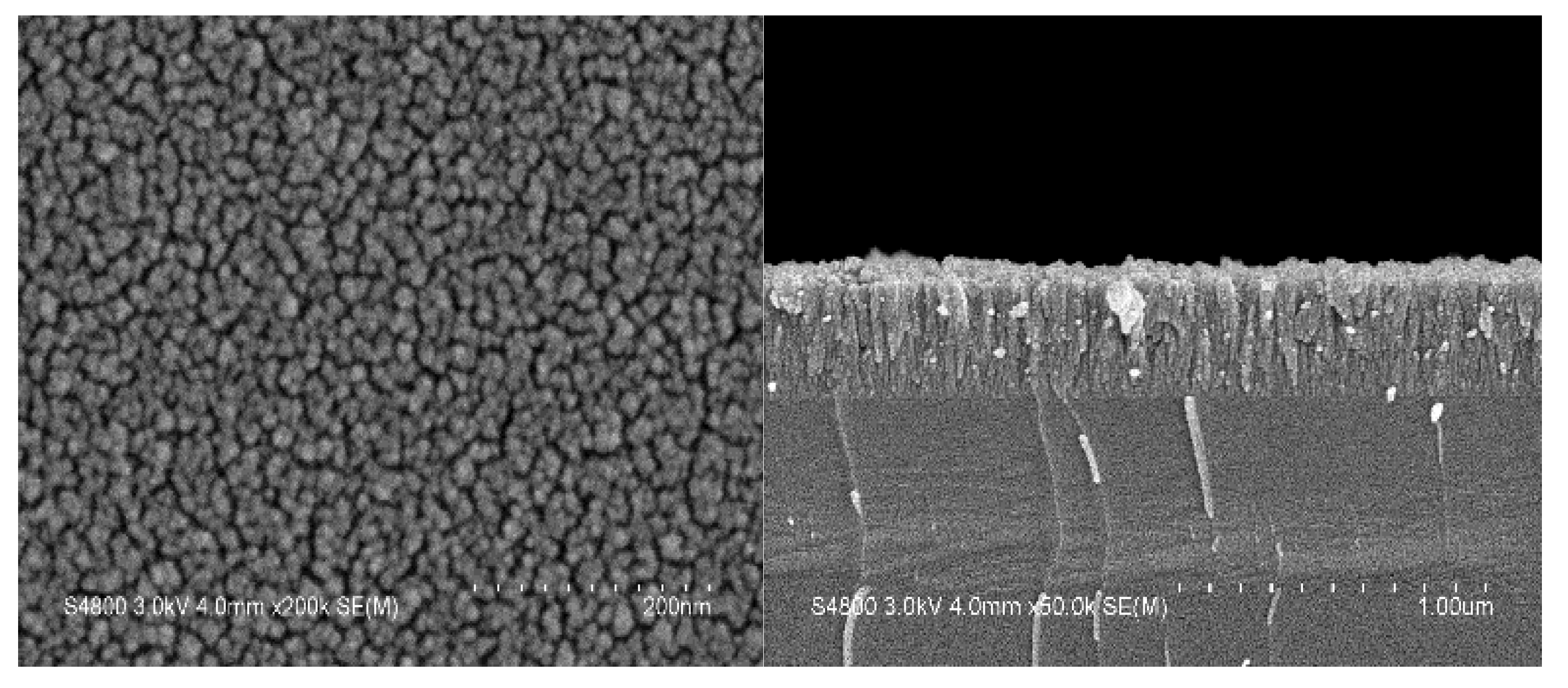
3.3.2. Surface Morphology of Undoped VO2 and W-Doped VO2 Thin Films
The surface morphology and cross-sections of the VO2 thin films were characterized using a high-resolution field emission scanning electron microscope (FE-SEM). The film’s microstructure analysis is based on scanning electron microscope (SEM) measurements of cross-sectional and top-down views of vanadium dioxide thin films. Figure 11 and Figure 12 show the SEM images of undoped VO2 and 5% W-doped VO2 thin films. With the addition of tungsten doping, larger and more densely dispersed particles are observed on the surface of the thin films. In contrast, undoped VO2 thin films exhibit smaller particles. The larger ionic radius of tungsten compared to vanadium affects the stability and activity of grain boundaries, making them more prone to movement. This results in the potential migration and coalescence of existing grains at the grain boundaries, leading to the enlargement of crystal grains in the vanadium dioxide thin films.
4. Conclusions
This study employed an electron gun evaporation combined with an ion-assisted deposition technique to fabricate tungsten-doped vanadium dioxide thin films with doping contents of 3%, 4%, and 5%, as well as undoped VO2 thin films. All deposited VO2 thin films have a thickness of 100 nm. This investigation revealed that higher W doping contents resulted in lower transmittance in the visible light spectrum (400-750 nm) and the infrared spectrum (2.5 μm to 5.5 μm). Along with the phase transition, the optical and electrical properties of VO2 films undergo significant changes. Meanwhile, as the W doping ratio increases, the residual stress in the VO2 thin film gradually decreases and the surface roughness increases. Optimal stress levels can be found to enhance the durability of the thin films. The thin film heating experiment showed that compared with other doped VO2 films and undoped films, the transmittance of 5% W-doped VO2 films decreased by about 11%. The Raman spectral peaks of the W-doped VO2 thin films and undoped VO2 thin films are consistent with the literature [30]. All four VO2 thin films feature a signature Raman peak at 612 cm−1. Future work may involve scaling up the deposition of W-doped VO2 thin films on larger substrates and optimizing process parameters for potential applications in smart glass windows, tunable optical filters and optical switches.
Author Contributions
Conceptualization, C.-L.T.; writing—original draft, C.-L.T. and M.-Y. L.; writing—review & editing, C.-L.T.; validation: C.-L.T. and M.-Y. L.; funding acquisition, C.-L.T.; visualization, M.-Y. L. and C,-C. W; resources, C,-C. W.; data curation: S.-C. L. All authors have read and agreed to the published version of the manuscript.
Funding
Please add: This study was supported in part by the National Science and Technology Council (NSTC), R.O.C., under project number NSTC 112-2221-E-008-082.
Data Availability Statement
Not applicable.
Acknowledgments
Authors are grateful for the National Science and Technology Council (NSTC) of Taiwan for the support of this research. This study was also supported by the Precious Instrument Center of Feng Chia University.
Conflicts of Interest
The authors declare no conflict of interest.
References
- Tain, J.; Peng, H.; Du, X.; Wang, H.; Cheng, X.; Du, Z. Hybrid thermochromic microgels based on UCNPs/PNIPAm hydrogel for smart window with enhanced solar modulation. Journal of Alloys and Compounds 2020, 858, 157725. [CrossRef]
- Chang, T.C.; Cao, X.; Bao, S.H.; Ji, S.D.; Luo, H.J.; Jin, P. Review on thermochromic vanadium dioxide based smart coatings: from lab to commercial application. Advances Manufacturing 2018, 6, 1–19. [CrossRef]
- Ji, Y.D.; Pan, T.S.; Bi, Z.; Liang, W.Z.; Zhang, Y.; Zeng, H.Z.; Wen, Q.Y.; Zhang, H.W.; Chen, C.L.; Jia, Q.X.; Lin, Y. Epitaxial growth and metal-insulator transition of vanadium oxide thin films with controllable phases. Appl. Phys. Lett. 2012, 101, 071902. [CrossRef]
- Meng, Y.; Huang, K.; Tang, Z.; Xu, X.; Tan, Z.; Liu, Q.; Wang, C.; Wu, B.; Wang, C.; Cao, J. The effect of Argon pressure dependent V thin film on the phase transition process of VO2 thin film. Applied Surface Science 2018, 427, Part B 304-311. [CrossRef]
- Bhupathi, S.; Wang, S.; Ke, Y.; Long, Y. Recent progress in vanadium dioxide: The multi-stimuli responsive material and its applications. Materials Science and Engineering 2023, 155, 100747. [CrossRef]
- Dou, S., Zhang, W., Wang, Y., Tian, Y., Wang, Y., Zhang, X., Zhang, L., Wang, L., Zhao, J., Li, Y. A facile method for the preparation of W-doped VO2 films with lowered phase transition temperature, narrowed hysteresis loops and excellent cycle stability. Materials Chemistry and Physics 2018, 215, 91-98. [CrossRef]
- Outón, J.; Casas-Acuña, A.; Domínguez, M.; Blanco, E.; Delgado, J.J.; Ramírez-del-Solar, M. Novel laser texturing of W-doped VO2 thin film for the improvement of luminous transmittance in smart windows application. Applied Surface Science 2023, 608, 155180. [CrossRef]
- Takami, H.; Kanki, T.; Ueda, S.; Kobayashi, K.; Tanaka, H. Filling-controlled Mott transition in W-doped VO2. Phys. Rev. B 2012, 85, 205111. [CrossRef]
- Ji, H.; Liu, D.; Cheng, H. Infrared optical modulation characteristics of W-doped VO2(M) nanoparticles in the MWIR and LWIR regions. Materials Science in Semiconductor Processing 2020, 119, 105141. [CrossRef]
- Ye, J.; Zhou, L. Preparation, characterization and properties of thermochromic tungsten-doped vanadium dioxide by thermal reduction and annealing. Journal of Alloys and Compounds 2010, 504, 503-507. [CrossRef]
- Lee, M.H.; Kim, M.G. RTA and stoichiometry effect on the thermochromism of VO2 thin films. Thin Solid Films 1996, 286(1–2), 219–222. [CrossRef]
- Hossain, M.I.; Mansour, S. A critical overview of thin films coating technologies for energy applications. Cogent Engineering 2023, 10, 2179467. [CrossRef]
- Tien, C. L.; Zeng, H. D. Measuring residual stress of anisotropic thin film by fast Fourier transform. Optics Express 2010, 18(16), 16594-16600. [CrossRef]
- Tien, C. L.; Yang, H.M.; Liu, M.C. The measurement of surface roughness of optical thin films based on fast Fourier transform. Thin Solid Films 2009, 517(17), 5110-5115. [CrossRef]
- Tien, C. L.; Yu, K.C.; Tsai, T.Y.; Lin, C.S.; Li, C.Y. Measurement of surface roughness of thin films by a hybrid interference microscope with different phase algorithms. Applied Optics 2014, 53 (29), H213-H219. [CrossRef]
- Begara, F. U.; Crunteanu, A.; Raskina, J. P. Raman and XPS characterization of vanadium oxide thin films with temperature. Applied Surface Science 2017, 403, 717-727. [CrossRef]
- Gomez-Heredia, C. L.; Ramirez-Rincon, J.A.; Bhardwaj, D.; Rajasekar, P.; Tadeo, I. J.; Cervantes-Lopez, J. L.; Ordonez-Miranda, J.; Ares1, O.; Umarji, A. M.; Drevillon, J.; Joulain, K.; Ezzahri, Y.; Alvarado-Gil, J. J. Measurement of the hysteretic thermal properties of W-doped and undoped nanocrystalline powders of VO2. Scientific Reports 2019, 9, 14687. [CrossRef]
- Mulchandani, K.; Soni, A.; Pathy, K.; Mavani, K.R. Structural Transformation and Tuning of Electronic Transitions by W-Doping in VO2 Thin Films. Superlattices Microstruct. 2021, 154, 106883. [CrossRef]
- Schilbe, P. Raman Scattering in VO2. Phys. B Condens. Matter 2002, 316–317, 600–602. [CrossRef]
- Jung, K. H.; Yun, S. J.; Slusar, T.; Kim, H.T.; Roh, T. M. Highly transparent ultrathin vanadium dioxide films with temperature-dependent infrared reflectance for smart windows. Applied Surface Science 2022, 589, 714-721. [CrossRef]
- Chen, S. E.; Lu, H. H.; Brahma, S. Effects of annealing on thermochromic properties of W-doped vanadium dioxide thin films deposited by electron beam evaporation. Thin Solid Films 2017, 644, 52-56. [CrossRef]
- Batista, C.; Ribeiro, R.M.; Teixeira, V. Synthesis and characterization of VO2-based thermochromic thin films for energy-efficient windows. Nanoscale Res. Lett. 2011, 6, 1–7. [CrossRef]
- Kittiwatanakul, S.; Laverock, J.; Newby, D.; Smith, K.E.; Wolf, S.A.; Lu, J. Transport behavior and electronic structure of phase pure VO2 thin films grown on c-plane sapphire under different O2 partial pressure. J. Appl. Phys. 2013, 114, 053703. [CrossRef]
- Zhang, D.P.; Zhu, M.D.; Liu, Y.; Yang, K.; Liang, G.X.; Zheng, Z.H.; Cai, X. M.; Fan, P. High performance VO2 thin films growth by DC magnetron sputtering at low temperature for smart energy efficient window application. J. Alloys Compd. 2016, 659, 198–202. [CrossRef]
- Kumar, M.; Singh, J. P.; Chae, K.H.; Park, J.; Lee, H.H. Annealing effect on phase transition and thermochromic properties of VO2 thin films. Superlattices and Microstructures 2020, 137, 106335. [CrossRef]
- Lu, Q.; Bishop, S. R.; Lee, D.; Lee, S.; Bluhm, H.; Tuller, H. L.; Lee, H. N.; Yildiz, B. Electrochemically Triggered Metal-Insulator Transition between VO2 and V2O5. Advanced Functional Materials 2018, 28, 1803024. [CrossRef]
- Thurn, J.; Hughey, M. P. Evaluation of film biaxial modulus and coefficient of thermal expansion from thermoelastic film stress measurements. J Appl Phys. 2004, 95(12), 7892–7897. [CrossRef]
- Gao, C.; Zhao, Z.; Li, X. Modeling of thermal stresses in elastic multilayer coating systems. Journal of Applied Physics 2015, 117(5), 055305. [CrossRef]
- J. Ye, J.; Zhou, L. Preparation, characterization and properties of thermochromic tungsten-doped vanadium dioxide by thermal reduction and annealing. Journal of Alloys and Compounds 2010, 504, 503-507. [CrossRef]
- Huang, Z.; Chen, C., Lv, C.; Chen, S. Tungsten-doped vanadium dioxide thin films on borosilicate glass for smart window application. Journal of Alloys and Compounds 2013, 564, 158-161. [CrossRef]
Figure 1.
Transmittance spectra of undoped and W-doped VO2 thin films.
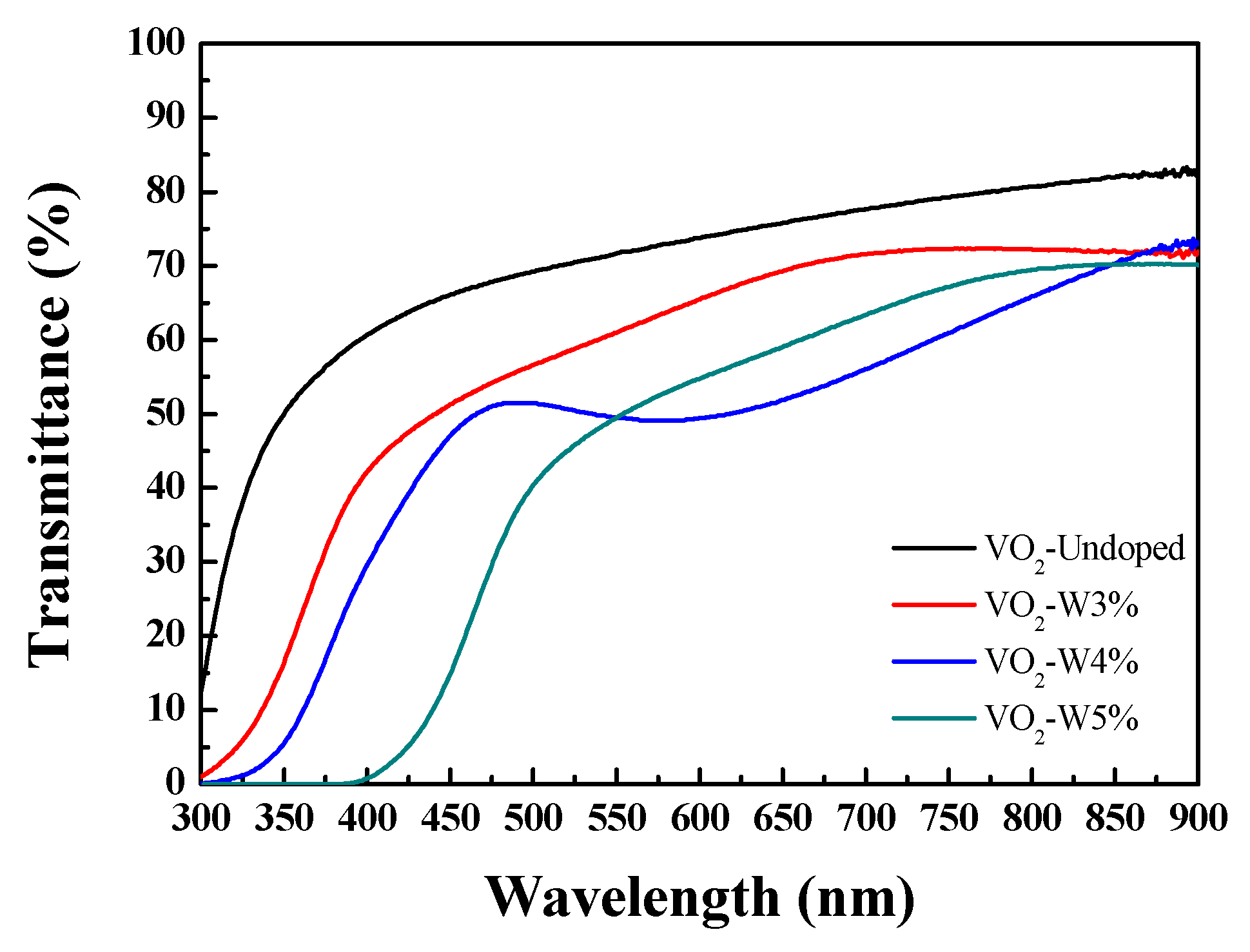
Figure 2.
Infrared transmittance spectra of undoped and W-doped VO2 thin films.
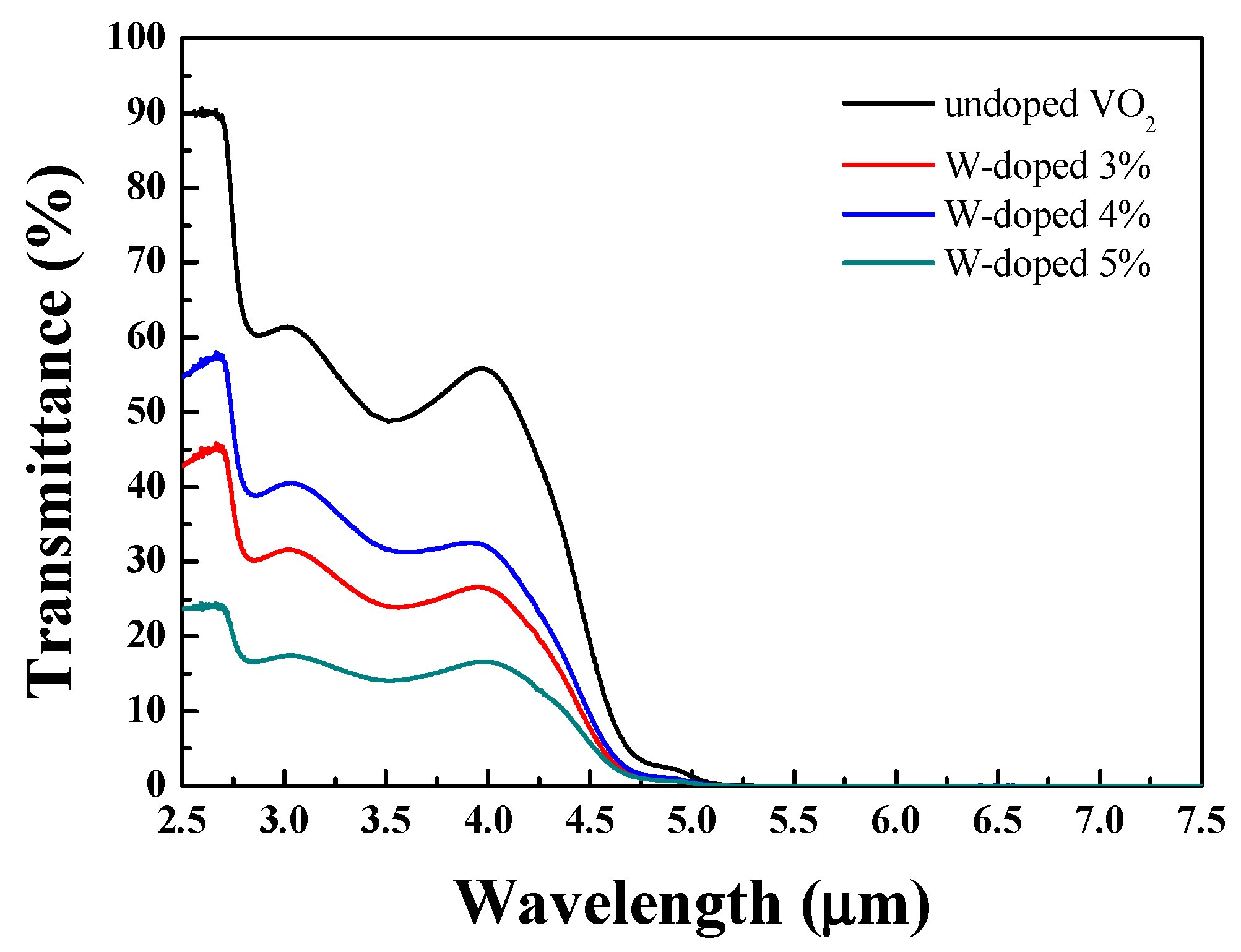
Figure 3.
The refractive index of VO2 thin films with different W-doped contents.
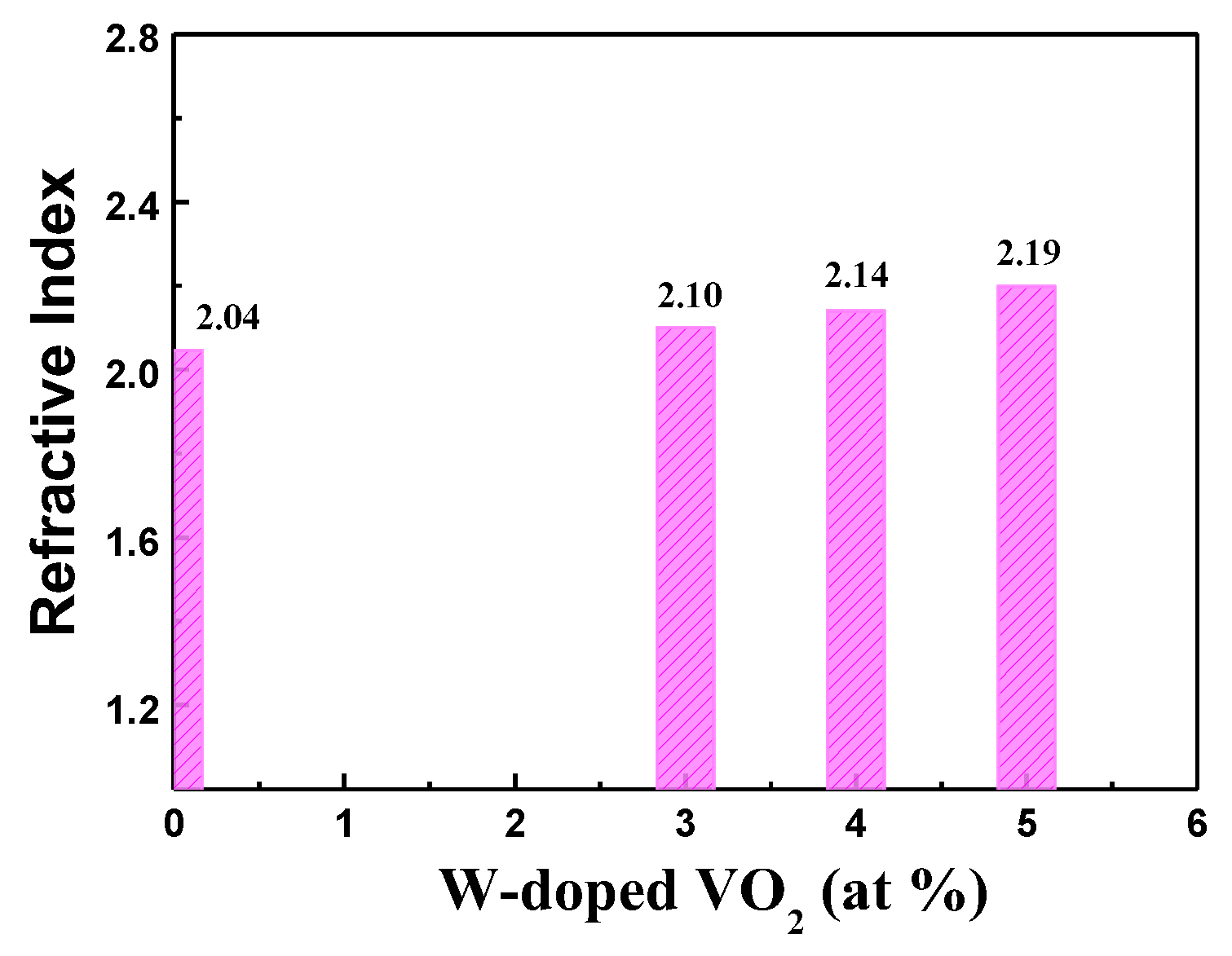
Figure 4.
Raman spectra of undoped and tungsten-doped vanadium dioxide thin films.
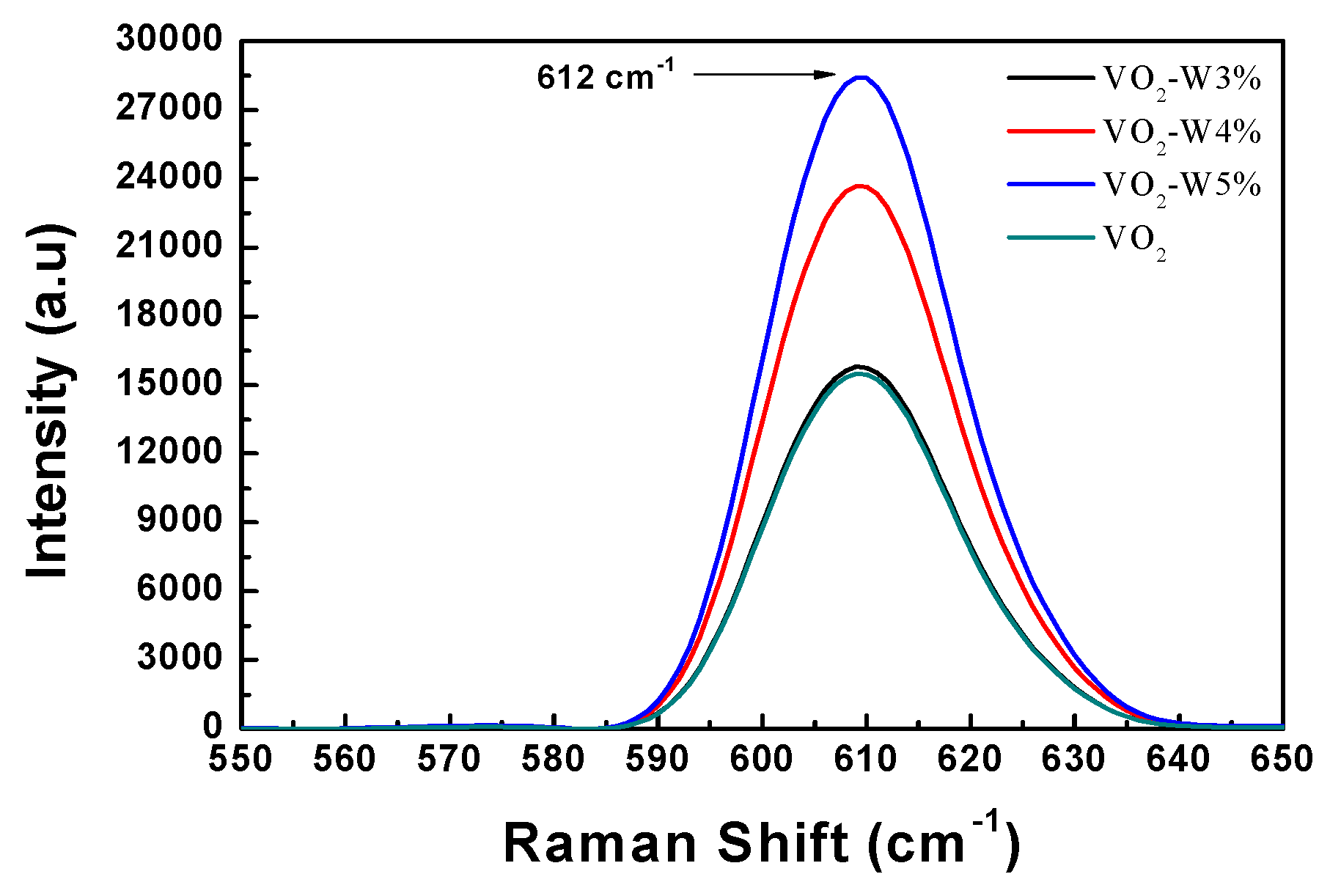
Figure 5.
Transmittance of undoped and W-doped VO2 thin films as a function of heating temperatures.
Figure 5.
Transmittance of undoped and W-doped VO2 thin films as a function of heating temperatures.
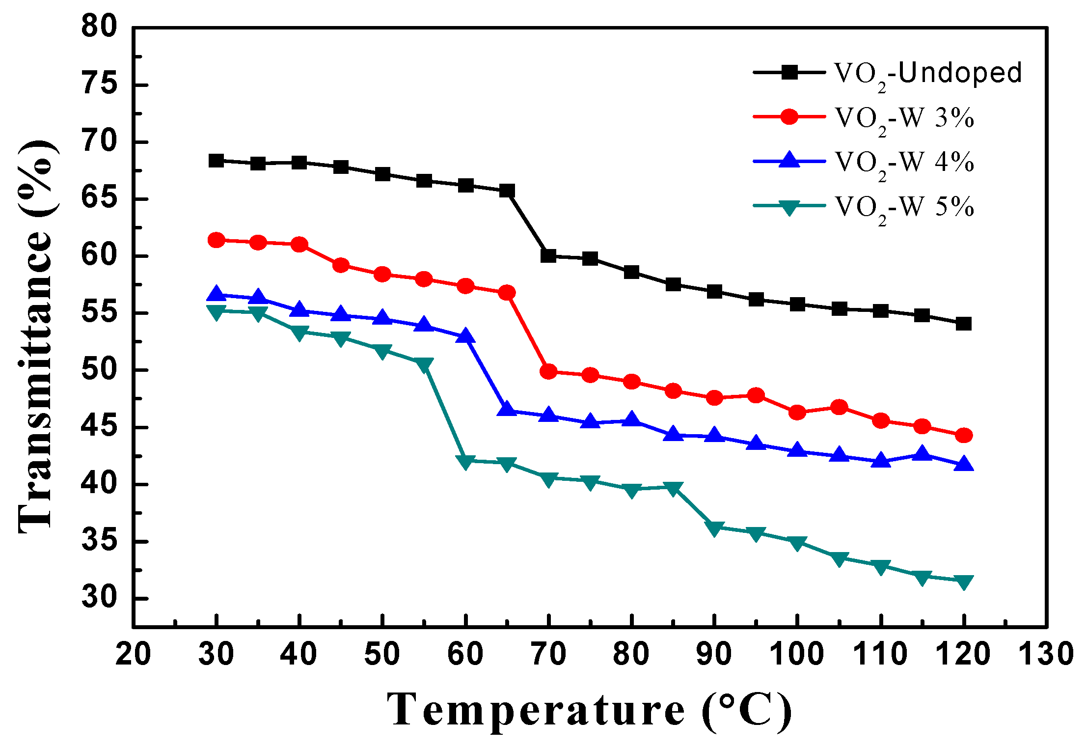
Figure 6.
Residual stress of undoped VO2 and W-doped VO2 thin films.
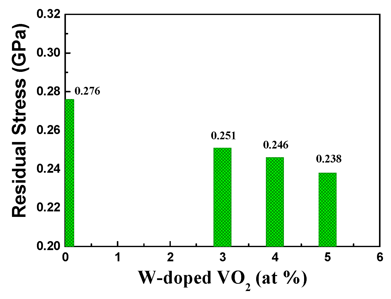
Figure 7.
Surface roughness of undoped VO2 and W-doped VO2 thin films.
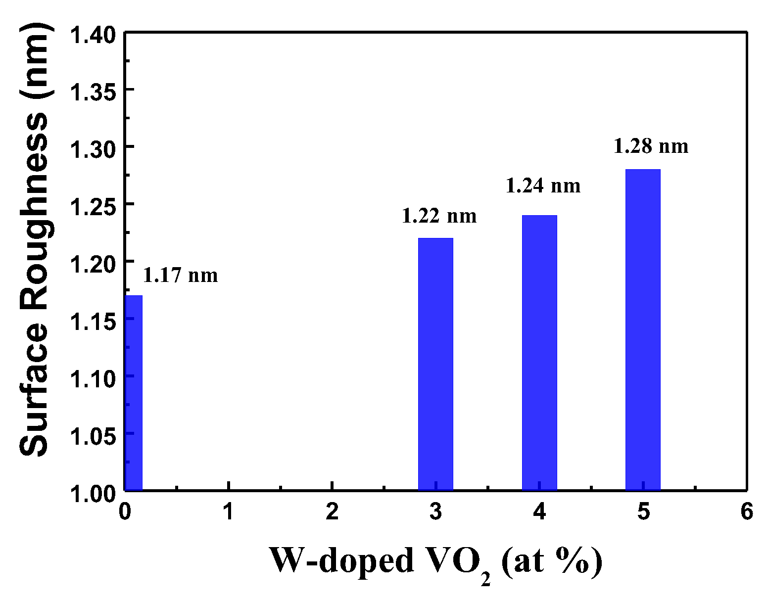
Figure 8.
Residual stress as a function of heating temperature for 5% W-doped VO2 thin films deposited on dual substrates.
Figure 8.
Residual stress as a function of heating temperature for 5% W-doped VO2 thin films deposited on dual substrates.
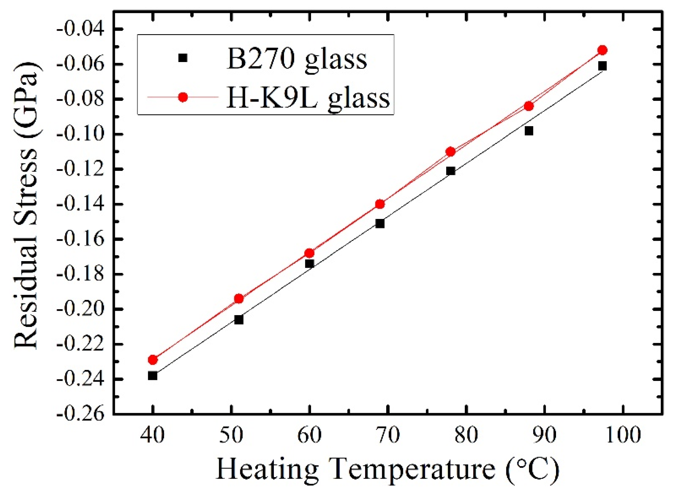
Figure 9.
Temperature-dependent resistivity of undoped VO2 and W-doped VO2 thin Films.
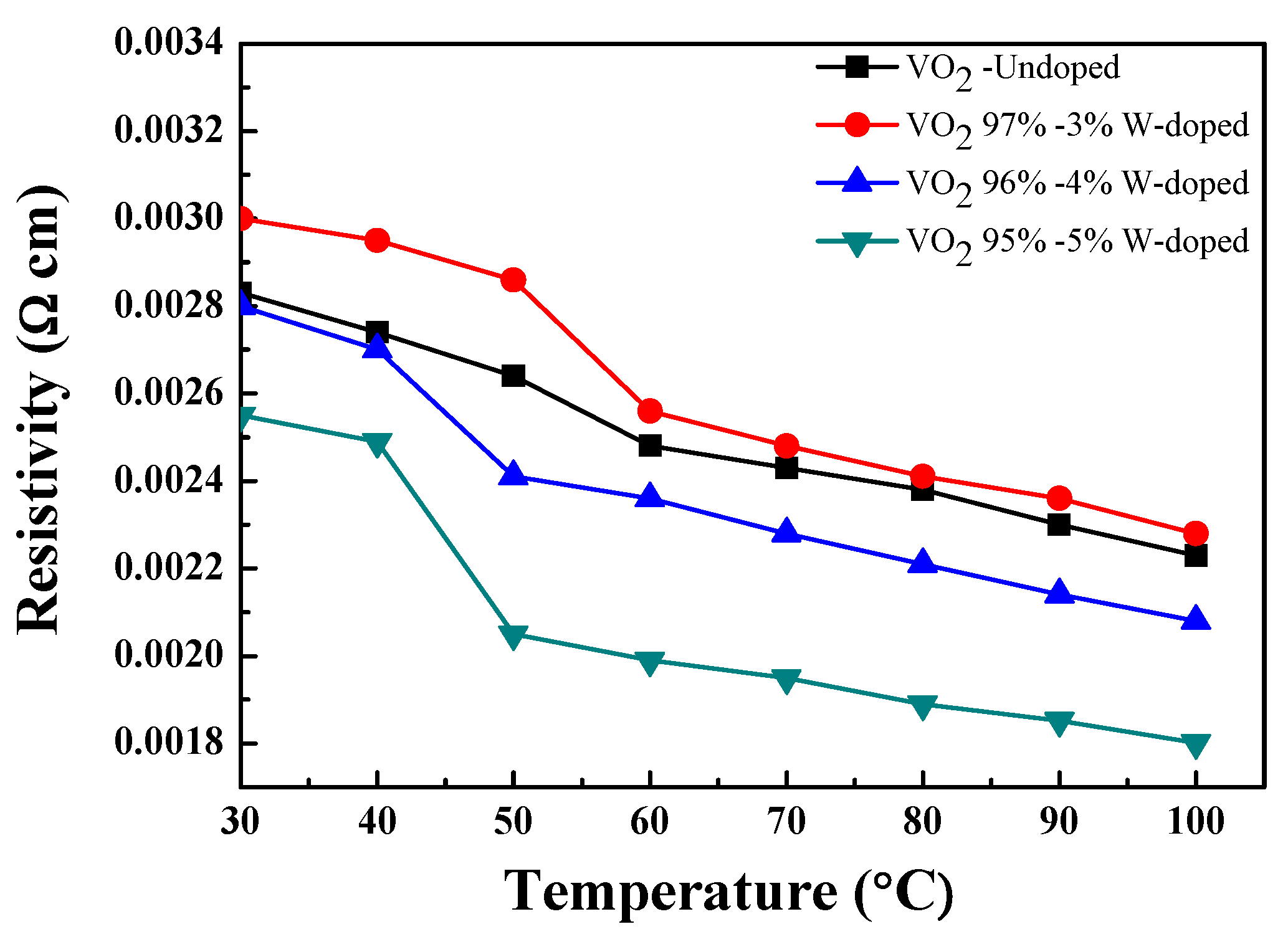
Figure 10.
X-ray diffraction (XRD) pattern of 5% W-doped VO2 thin film.
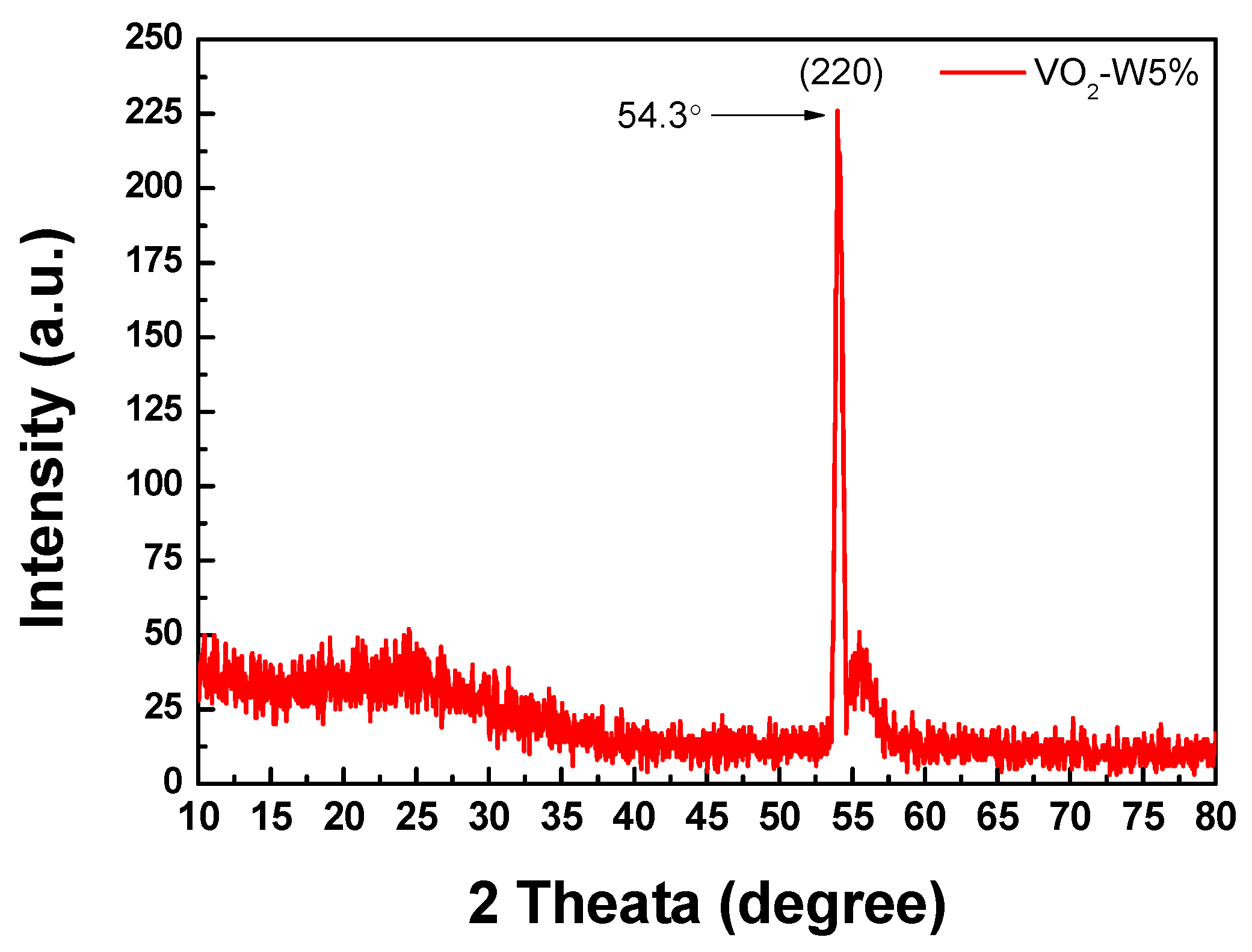
Figure 11.
SEM images of undoped VO2 thin films: (Left) Top-down view, (Right) Cross-sectional view.
Figure 11.
SEM images of undoped VO2 thin films: (Left) Top-down view, (Right) Cross-sectional view.
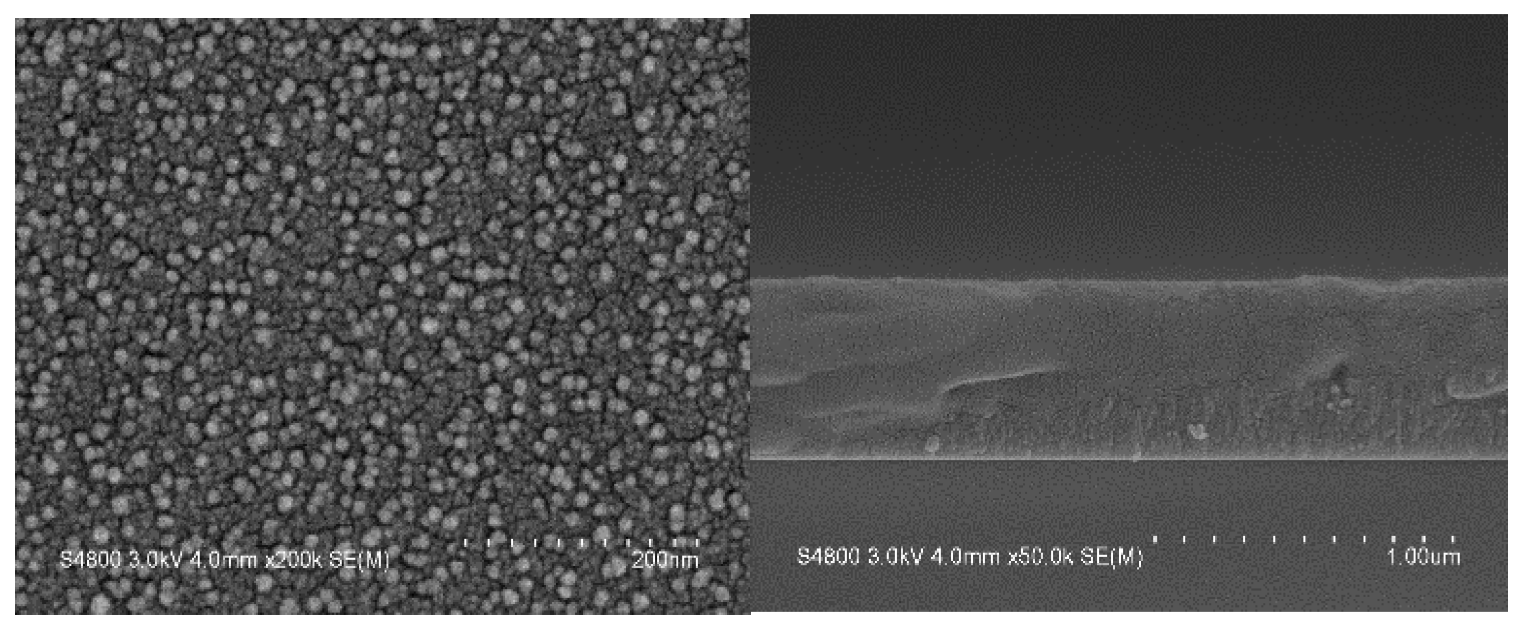
Figure 12.
SEM images of 5% W-doped VO2 thin film: (Left) Top-down view, (Right) Cross-sectional view.
Figure 12.
SEM images of 5% W-doped VO2 thin film: (Left) Top-down view, (Right) Cross-sectional view.
Disclaimer/Publisher’s Note: The statements, opinions and data contained in all publications are solely those of the individual author(s) and contributor(s) and not of MDPI and/or the editor(s). MDPI and/or the editor(s) disclaim responsibility for any injury to people or property resulting from any ideas, methods, instructions or products referred to in the content. |
© 2024 by the authors. Licensee MDPI, Basel, Switzerland. This article is an open access article distributed under the terms and conditions of the Creative Commons Attribution (CC BY) license (http://creativecommons.org/licenses/by/4.0/).
Copyright: This open access article is published under a Creative Commons CC BY 4.0 license, which permit the free download, distribution, and reuse, provided that the author and preprint are cited in any reuse.


