Submitted:
13 February 2025
Posted:
17 February 2025
Read the latest preprint version here
Abstract
This study provides a comprehensive characterization of various isolated single and half-bridge gate drivers over the entire temperature range from room temperature down to -194 °C. Unlike previous studies, which primarily focused on electrical output parameters such as rise/fall times and propagation delays, this paper also explores critical functionalities like undervoltage lockout (UVLO) and common-mode transient immunity (CMTI). In general, most drivers demonstrate a trend toward reduced rise/fall times and propagation delays as temperatures decreased. The UVLO threshold of most gate drivers tested was found to be quite stable down to low temperatures, but with exceptions. The first comprehensive characterization of the power-up and -down behavior of gate drivers identified critical operating states for practical use. In addition, CMTI testing revealed premature functional failures of some drivers at low temperatures.
Keywords:
cryogenic
; common mode transient immunity
; CMTI
; device characterization
; driver IC
; low temperature
; power electronics
; undervoltage lockout
1. Introduction
Cryogenic power electronics offer the potential to significantly improve the overall system efficiency, particularly as part of superconducting propulsion systems for future electric aircrafts. However, this advancement requires the careful selection of electronic components that not only perform reliably at cryogenic temperatures but also enhance the efficiency of the entire power electronics system. Consequently, many studies have focused on characterizing both passive and active electronic components at low temperatures. The greatest potential for reducing power losses at cryogenic temperatures lies in semiconductor devices based on silicon and gallium nitride (GaN) [1]. However, power electronics consist of more than just power semiconductors. In particular, the components of the commutation cell and the driver circuit must be placed close to the power semiconductors, meaning they too are exposed to low temperatures. As modern wide-bandgap (WBG) semiconductors are switched at increasingly high speeds, it becomes crucial to position driver circuits near the power switches in order to minimize parasitic elements, such as lead inductances. Since no commercially available driver is fully specified for operation at temperatures as low as liquid nitrogen (LN2, -196 °C), this study presents a detailed characterization of various single and half-bridge drivers.
Although several studies have investigated driver performance at low temperatures, these often focus on individual electrical parameters such as rise/fall times and propagation delay [2,3,4,5], or are limited to measurements at a single temperature, typically 77 K [6]. As a result, these studies do not provide a comprehensive understanding of the functional temperature range. Furthermore, in some publications, the measurement conditions are not adequately described, or driver ICs are tested with auxiliary power supply components at low temperatures, which can affect the driver's temperature behavior and obscure its actual performance [6,7]. Previous studies, as well as our own investigations, have shown that ICs based on Si-CMOS technology can operate at -196 °C, while bipolar and BiCMOS technologies predominantly exhibit functional failures at such low temperatures [1]. Therefore, this study focuses on commercially available isolated CMOS driver ICs, which currently dominate the market. In addition to driver output characterization, we examine critical performance aspects such as the behavior of the undervoltage lockout (UVLO) and common mode transient immunity (CMTI) over the entire temperature range from room temperature down to cryogenic temperatures.
2. Application Aspects
Gate drivers (highlighted in green in Figure 1 for single gate drivers) serve as the interface between the signal generation and the power semiconductor switch, performing several key functions. Their primary role is to ensure precise switching transitions by delivering the required voltage levels to the gate of a power transistor. This enables the transistor to switch efficiently and reliably between fully conducting and blocking states, while preventing undesired switching events. Another important function of the driver IC is to amplify the current of a typically digital control signal to enable fast charging and discharging of the gate, thereby shortening switching times and minimizing switching losses. Additionally, isolating gate drivers can provide galvanic isolation between the control and load circuits, ensuring electrical separation and enhancing system safety. The most relevant parameters of an isolating driver circuit, which can also be temperature dependent, are:
- rise time and fall time of the driver output stage,
- output current source and sink capability,
- logical functionalities as propagation delay and undervoltage lockout (UVLO),
- common mode transient immunity (CMTI).
CMTI is the robustness of a driver against fast voltage transients across the isolation barrier without malfunctions and failures occurring. This is important because very high voltage gradients occur in power electronic converters due to the switching processes, which can affect the proper circuit functionality and thus the reliability of a system. As illustrated in Figure 1, the so-called Miller effect in a half-bridge circuit also poses a significant challenge, as it can lead to undesired switching events, particularly parasitic turn-on (PTO), resulting in excessive heating and potential damage. When the high-side transistor is turned on, for example, a steep voltage rise dvds/dt occurs at the low-side transistor, causing a current idg to flow via Cgd and the gate resistor Rg to the source or ground. At this moment, the low-side transistor, which must remain “OFF” (vgs = 0 V), experiences a voltage pulse at its gate due to the current passing through the gate resistor. This pulse, however, must not exceed the threshold voltage of the transistor, otherwise a destructive short circuit would occur in the power semiconductor half-bridge (T1, T2). It is important to note that the temperature-dependent behavior of the threshold voltage varies on the transistor material. In standard Si MOSFET, for example, the threshold voltage (typ. 2 to 4 V at 20 °C) increases by approx. 30% at -196 °C [8,9]. The threshold voltage of GaN HEMTs (typ. 1.1 to 1.6 V @ 20 °C) shows lower temperature dependence. This voltage can increase by approximately 15% down to -196 °C [9,10], but in some cases, depending on the HEMT technology, it can also show a decrease of up to 30% [10].
3. Characterization Method
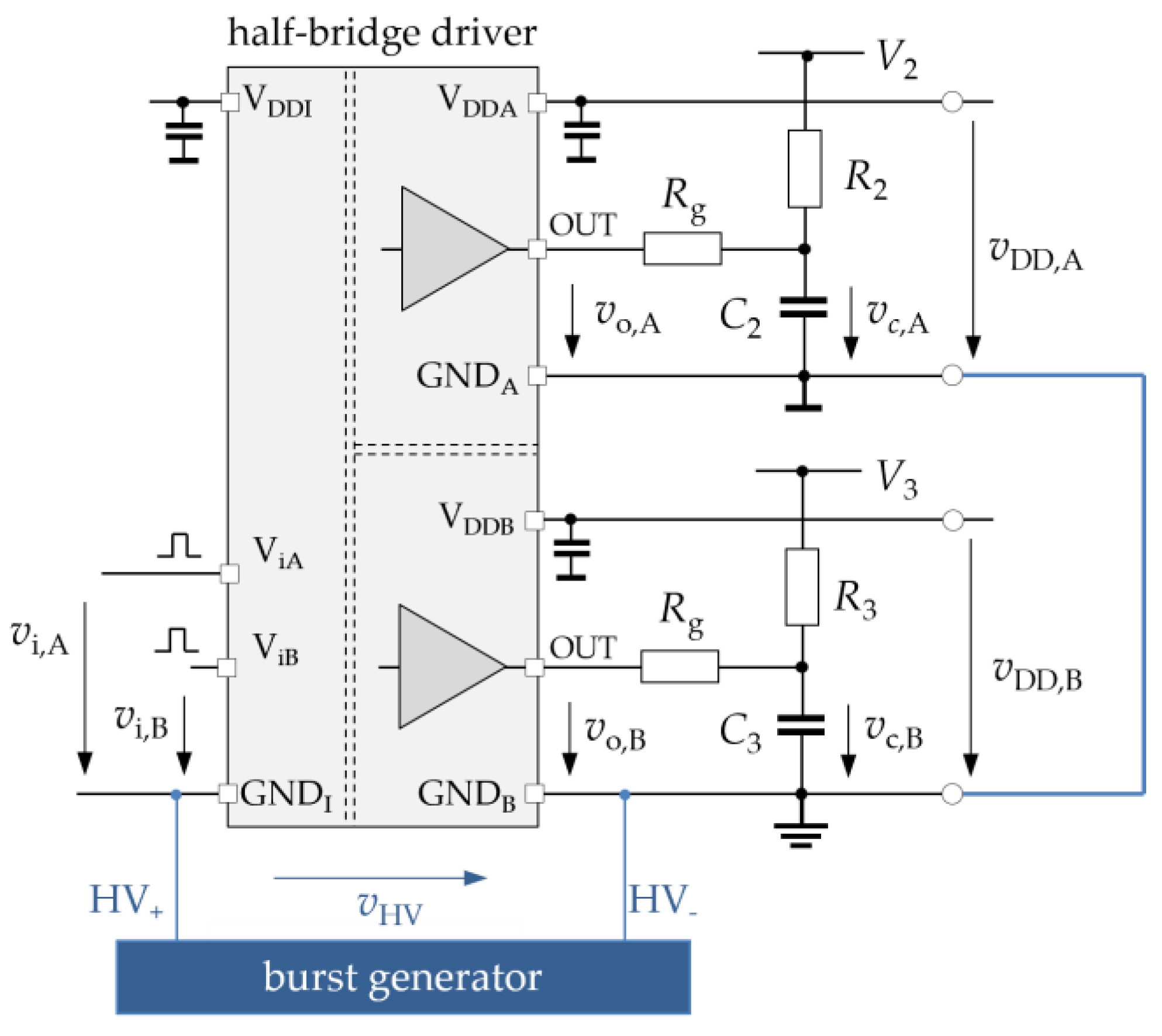
To date, only the fundamental functions and performance parameters of the output stage of a driver have been characterized [2,3,4,5,6,7]. However, this paper presents, for the first time, a detailed characterization of commercially available driver ICs from room temperature down to cryogenic temperatures, considering all relevant parameters of a driver circuit as outlined in section 2. The test circuits and measurement methods used for this characterization are illustrated in the following figures. Figure 2 shows a simplified schematic of the test circuit with the recorded voltages for a single driver, Figure 4 illustrates the test circuit and measurement signals at the half-bridge drivers. On the input side, the drivers receive a square wave digital signal vi from a signal generator and a supply voltage VDDI. By only briefly pulsing the square wave signals, it can be assumed that the chip temperature closely corresponds to the case temperature of the driver. A gate resistor Rg can be positioned at the outputs of the drivers if necessary. Instead of the gate of a power FET, a highly linear and temperature stable NP0 capacitor Ci (i = 1,2,3) is used as a dummy load, with capacitance values set at 2 nF (for single drivers) and 4.7 nF (for half bridge drivers). This choice was made to intentionally exceed the input capacitances Ciss of typical Si or GaN transistors, allowing for an effective evaluation of the output current capability of the drivers. Pull-up resistors Ri (i = 1,2,3) with 24 kΩ at the driver outputs are utilized to inject a small current in the mA range. This allows to detect whether the driver shows forbidden undefined floating potentials at its output, which can be fatal in practical applications due to the Miller effect. All voltage and passive component values used in the respective test circuits are listed alongside the tested single and half bridge drivers in Table 1.
The measurement results are presented in section 4. Subchapter 4.1 first discusses the low-temperature behavior of the driver output parameters. The rise time and the fall time of the output signal vo (or vo,A/B) are defined as the time required for the voltage to change from its 10% to 90% level (or vice versa). Subchapter 4.2 and 4.3 examine relevant parameters of the driver's logic functional units at low temperatures. This includes propagation delay of the signal through the driver (4.2) as well as the undervoltage lockout threshold (4.3). The propagation delay is defined as the time difference, measured at 50% of input-output transition, after application of a signal to the input. A distinction is made between the “low to high” and “high to low” signal transition.
The test method for determining the undervoltage lockout turn-on (positive-going) and turn-off (negative-going) threshold values is shown in Figure 3. While a periodic square-wave input signal is applied, the driver voltage vDD (vDD,A/B) is gradually increased and decreased according to a ramp function, and the output signal is recorded throughout this process. As long as the driver supply voltage is below the undervoltage lockout (UVLO) threshold specified in the data sheet, the output should remain active zero. This requirement also applies during the descending ramp of the supply voltage: Once the voltage falls below the UVLO threshold, the output signal must drop to zero and actively fixed at that level until the UVLO threshold is exceeded again. This undervoltage monitoring is essential for a safe operation of the power semiconductor switches, as an activation with too low gate voltage levels will result in destructive losses in the power switch. The supply voltage ramp simulates a situation that can occur in many applications, especially when the supply voltage (e.g. vDD,A in Figure 4) is generated via a bootstrap circuit. In this case, it may take several switching cycles to reach a stable supply voltage level after power-up.
Common mode transient immunity CMTI is another critical parameter of high-side gate drivers that describes a device's immunity to transient common mode disturbances and defines the allowable voltage gradient dv⁄dt that can be applied without compromising an error-free and reliable operation. This applies to both positive and negative voltage gradients. Due to parasitic capacitive coupling of the primary and secondary side, fast transients can pass through the isolation barrier and thus can lead to faulty behavior of the driver. False triggering and timing errors - such as delayed or missing switching pulses - can result in malfunctions or even permanent damage of the power transistor. Incomplete or erratic switching operations can lead to excessive heat generation, further increasing the risk of failure. Common test procedures from datasheets can be utilized to evaluate the CMTI, as demonstrated in Figure 4. By applying controlled transient common mode voltages vHV across the two ground references of the gate driver, the output signals vo,A/B (or vo) can be monitored to evaluate the drivers’ performance. Care was taken to ensure that the high-voltage signal vHV from the burst generator (Schlöder SFT1420) did not exceed the transient isolation voltage specified for each test object (DUT).
For the CMTI tests, the secondary side was chosen as the reference ground. The high voltage input side was powered by a 9 V battery followed by a linear regulator (LDO) to provide the required primary side supply voltage (5 or 3.3 V), and the control signals were applied via fiber optics. Both to minimize ground coupling effects. Battery, LDO and fiber optic receivers were placed outside the cryo-chamber with a short coax-cable for the signal to the DUT board inside the chamber, terminated with 50 Ω close to the DUT input, and supply voltage blocking capacitors close to the DUT. The supply voltage for the output side is provided from a laboratory power supply. Since the highly sensitive probes for measuring all voltages should not be exposed to cryogenic temperatures, it is important to keep also the twisted cables leading to the outside for signal measurement as short as possible. To address this, a special cooling chamber with comparable thin insulation thickness was developed (see Figure 5), smaller than the one described in [11]. As shown in Figure 6 this cooling chamber, operated with liquid nitrogen, can be utilized to set and maintain well-defined temperatures, ranging from room temperature down to a minimum of -194 °C on the DUT. Thermocouples are attached to the test board and the device under test to control and monitor the temperatures. The CMTI test results are presented in subchapter 4.4.
Figure 4.
CMTI test circuit using the example of a half-bridge driver.
4. Test results
4.1. Driver Output
The driver output stage is a critical element for precisely controlling the power transistor, enabling rapid and reliable switching between conducting and non-conducting states. The main functions of the output stage include providing the necessary voltage to ensure full turn-on of the transistor and providing high source and sink currents to rapidly charge and discharge the gate capacitance in order to reduce the on and off times, resulting in low switching losses.
The output stage of gate drivers is usually implemented as a complementary MOSFET stage as shown in Figure 12 in a simplified manner and in many cases with separately accessible drain terminals, which simplifies the control of the on and off times of the power transistor by means of individual gate resistors. The current source and sink capabilities of the driver directly determine the rise and fall times at a given load capacitance. Conversely, the mean output current capability can be determined from the measured rise and fall times at a fixed, known linear load capacitance:
To determine the maximum current source and sink capability of each IC, measurements were performed without an external gate resistor unless otherwise noted and using a highly stable (NP0) linear load capacitance. The source and sink capability is mainly determined by the output MOSFETs saturation characteristic and on-state resistance. Of course, any smaller gate current can be set in the application using additional external gate resistors. The designations in (1) refer to Figure 2 but are also transferable to Figure 4. In case of the ADUM4121 a non-zero gate resistance was used according to datasheet recommendations to avoid excessive output ringing. The same was done with the 2EDF7275F. Figure 7 shows the measured temperature-dependent output voltage using the Si8271 as an example. As can be seen, the rise and fall times decrease slightly with temperature, which also results in a slightly increased ringing.
In general, as can be seen in Figure 8 and Figure 9, most gate drivers show decreasing rise and fall times, i.e. increasing current capability with lower temperatures. In each diagram, the second y-axis (right) shows the current source and sink capability calculated from the measured rise and fall times according to (1). Please note that this is the more application-relevant average current capability and may somewhat differ from the peak current specified in the respective datasheet. The increasing current capability with lower temperatures is as expected, since with decreasing temperature the on-resistance decreases and the saturation current increases for both the p- and n-channel Si-MOSFET in the driver output stage. However, individual "outliers" also show that this general tendency can be overlaid and even reversed by influences of the complex IC-internal circuitry.
Three test results are particularly noticeable:
- In general, the rise and fall times stay within a quite narrow window over the entire temperature range, where-by the fastest drivers exhibit the most stable behavior.
- The UCC5304 and UCC5350 could only be characterized down to -175 °C, the MAX22701 down to -150 °C, and the NCP51820 down to -90 °C. In all these cases no more output pulses were provided at lower temperatures. In case of the NCP51820, a look at the course of the UVLO threshold at low temperatures (s. Figure 16 (b)) indicates a problem with the IC-internal UVLO monitoring as a root cause. In case of the MAX22701, it is unclear whether the chip technology used is actually CMOS or BiCMOS. The latter would explain limitations at very low temperatures. For the UCC53xx devices, we observed a parameter scatter regarding the functional limit at low temperatures. Some examples delivered an output signal even down to -190 °C.
4.2. Propagation Delay
A driver IC comprises several functional blocks that control, amplify and transmit signals from the digital driver input to the output. The time it takes for an input signal to pass through these functional blocks is called the propagation delay. The propagation delay of a driver should be largely independent of temperature, since in general the delay is part of the control loop of a switch-mode converter. In particular, the turn-on and turn-off delay should run in parallel, otherwise the switching pulse length at the output changes over temperature compared to the time commanded at the input. This is highly undesirable, for example, when setting the dead time in a half-bridge, i.e. the period of time during which both transistors must be switched off to avoid bridge short circuits.
The measurement results are shown in Figure 10 and Figure 11. Since the low-side channel behaved very similarly to the high-side channel, only the propagation delay of the high-side channel of the half-bridge drivers is shown in Figure 11. If an external gate resistor had to be used, the propagation delay was measured behind Rg, i.e. using vc. The curves show a widely stable propagation delay with some exceptions: The turn-on delay of the MAX22701 (magenta) rises noticeable below -100 °C, while the turn-off delay shows only a slight increase. Against the general trend, the UCC5350 in Figure 10 and UCC21551 in Figure 11 show an increase in propagation delay towards very low temperatures. In this case, however, the measurements continue the trend already specified in the datasheet within the regular operating temperature range. As mentioned above, the MAX22701, NCP51820, UCC5304 and UCC5350 could not be characterized down to the lowest temperatures.
As can be seen, an individual experimental characterization is important because a prediction of the low-temperature behavior of the propagation delay is generally not possible without detailed information about the internal circuitry of a driver IC.
4.3. Undervoltage Lockout
An important logical function of a driver-IC, which is highly relevant for a reliable and efficient operation of the power semiconductors, is the undervoltage lockout. This internal protective function monitors the driver supply voltage (VDD or VDDA/B) and prevents inadequate control of the power transistor when the voltage is below a specified threshold. This prevents malfunctions and potential thermal damage caused by an increased on-state resistance and incomplete switching operations. For proper protection, the UVLO threshold must be selected to match the threshold window and the transfer characteristics of the power semi conductor to be controlled. To avoid oscilla tions around the UVLO threshold, this is provided with a hyste resis. This means that a higher supply voltage is required to activate the output (turn-on or positive-going threshold) than for the transi tion into the lockout state (turn-off or negative-going threshold). The UVLO function within a driver IC com prises several circuit blocks like compara tors and logic gates, each with its own temperature charac te ristic.
To monitor whether the driver output is able to provide a well-defined zero state when the IC is inactive, a pull-up resistor is used as illustrated in Figure 2 and Figure 4. The pull-up resistor R1/2/3 = 24 kΩ is connected to a fixed 12 V source and injects a current of about 0.5 mA simu lating a Miller effect situation.
The measured output voltage during ramping up and down of the driver supply voltage with an applied periodic input signal is shown in Figure 13 and Figure 14. As can be seen, no IC is able to pull the output down to zero voltage when zero supply voltage is applied. This can be explained by Figure 12. The diodes shown in parallel to the comple mentary MOSFETs of the driver output stage represent the intrinsic body diodes of the respective MOSFETs and are drawn with a diode symbol for illustration purposes only. As long as there is not enough voltage available to turn on neither the p-MOS nor the n-MOS in the driver out put, the injected current flows through the body diode of the p-MOS (red current path) and charges the capacitor at the driver supply pin.
Figure 12.
CMOS driver explaining the voltage situation in case of an inactive complementary MOSFET output stage.
Figure 12.
CMOS driver explaining the voltage situation in case of an inactive complementary MOSFET output stage.
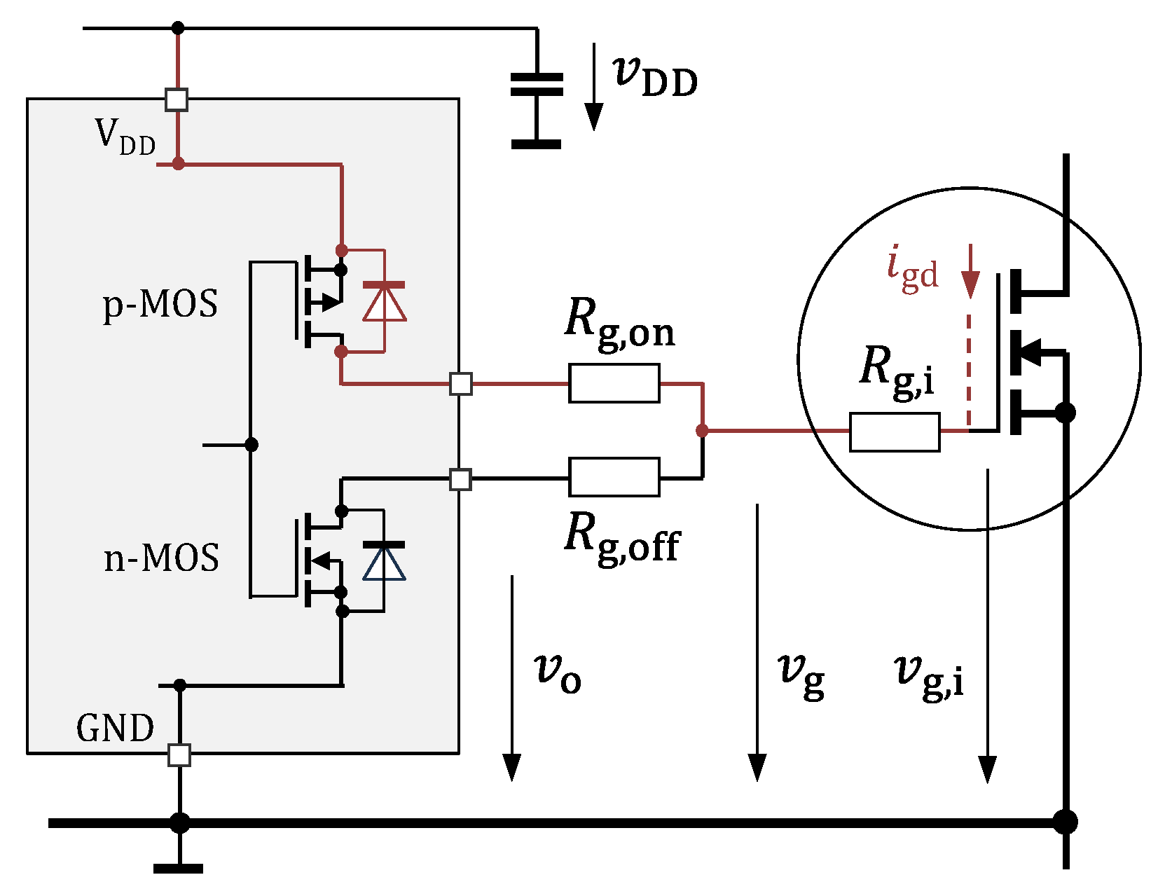
In this situation, the voltage vo at the driver output exceeds the supply voltage vDD by the forward voltage of the body-diode. Typically for Si p/n-diodes, this forward voltage in creas es with decreasing temperature and reaches about 0.8 V at -196 °C at the low in ject ed current in this test. As can be seen from Figure 13 and Figure 14, depending on the driver IC, the supply voltage must rise to over 2.5 V, before the n-MOS can be activated and the output is actively pulled to zero. The minimum supply voltage required for this in creases with decreasing tem pe ra ture, as does the threshold voltage of the n-MOS.
Notable exceptions are the single drivers UCC5304, UCC5350 and MAX22701 as well as the half bridge drivers 2EDF7275F and UCC21551. These obviously con tain an additional clamping circuit that ensures that the output voltage is limited already in this supply voltage range. However, even these devices cannot safely limit the output voltage to values below 1 V, even against the very low injection current chosen for the tests.
The floating state output voltage levels vary from approximately 1.0 V to 1.8 V at room tem pe rature to 1.5 V to 2.8 V at -194 °C. A similar behavior is observed in all drivers as the driver voltage decreases. Below a certain supply voltage, the driver is no longer able to apply an active zero state to its output.
A short numerical example should illustrate the problem: Assume that the power MOSFET has a Miller capacitance of Cgd = 20 pF and a dvds/dt = 50 V/ns occurs. Then a current idg = 1A is injected causing a voltage drop of 2 V across a typical chip internal gate resistance of Rg,i = 2 Ω. If the driver now allows an output voltage of 2.5 V when there is no or insufficient supply voltage, a voltage vg,i of 4.5 V occurs at the inner MOSFET gate, which already ex ceeds the typical threshold voltage of Si and SiC MOSFET. If there is an addi tio nal external gate resistor (Rg,on) in the circuit, the situation becomes even worse, and a parasitic turn-on be comes un avoidable. This problem becomes even more dramatic when GaN HEMTs with their low threshold voltage levels are to be controlled.
As soon as the driver's internal logic becomes functional, the output is actively pulled to zero. In the subsequent voltage range until the UVLO turn-on threshold is reached, no impermissible switching operations at the output (glitches) could be detected over the entire temperature range, for all drivers tested except the ADUM4221 (see Figure 14 (b)). The latter showed a pronounced malfunction near the UVLO threshold at very low temperatures with impermissible switch ing operations and phases in which the output stage is even deactivated again, which, as with supply voltages close to zero, becomes noticeable in output voltages above the driver supply voltage.
Immediately at the UVLO turn-on and turn-off threshold, all gate drivers showed a pulse shortening due to a lack of synchronization between the UVLO enable of the output and the control or input pulses. From an application point of view, however, this is generally not critical issue.
Above the UVLO threshold and within the functional temperature range shown in Figure 8 and Figure 9, all drivers pro vided regular output pulses with a level corres ponding to the driver supply voltage. At the frequency of 1 kHz used for the tests, these pulses are only visible as colored areas in the diagrams. However, the integrity of the output pulses within the regular operating range, i.e. above UVLO, was verified in all cases, especially at low tempe ra tures.
As can be seen from Figure 13 and Figure 14, the power-up and down behavior of all drivers examined is largely sym me tri cal. The non-linear decay of the supply voltage is due to the property of the programmable DC voltage source used, which could pro vide very small output voltages only with limited dynamics due to the lack of active sink capability. However, this shape is very close to the real supply voltage curve in an application after power-off.
In addition to investigating the behavior of the output stage within the UVLO operating range, an important objective of this test was to analyze the temperature de pendence of the driver's UVLO threshold. The dashed lines in Figure 13 and Figure 14 give the UVLO threshold range as speci fied in the respective datasheet for room temperature. An overview of the test results for both the positive and negative-going UVLO thresholds as a function of tempe ra ture is presented in Figure 15 and Figure 16.
Figure 15.
Positive-going (a,b) and negative-going (c,d) UVLO threshold of the single drivers over temperature.
Figure 15.
Positive-going (a,b) and negative-going (c,d) UVLO threshold of the single drivers over temperature.
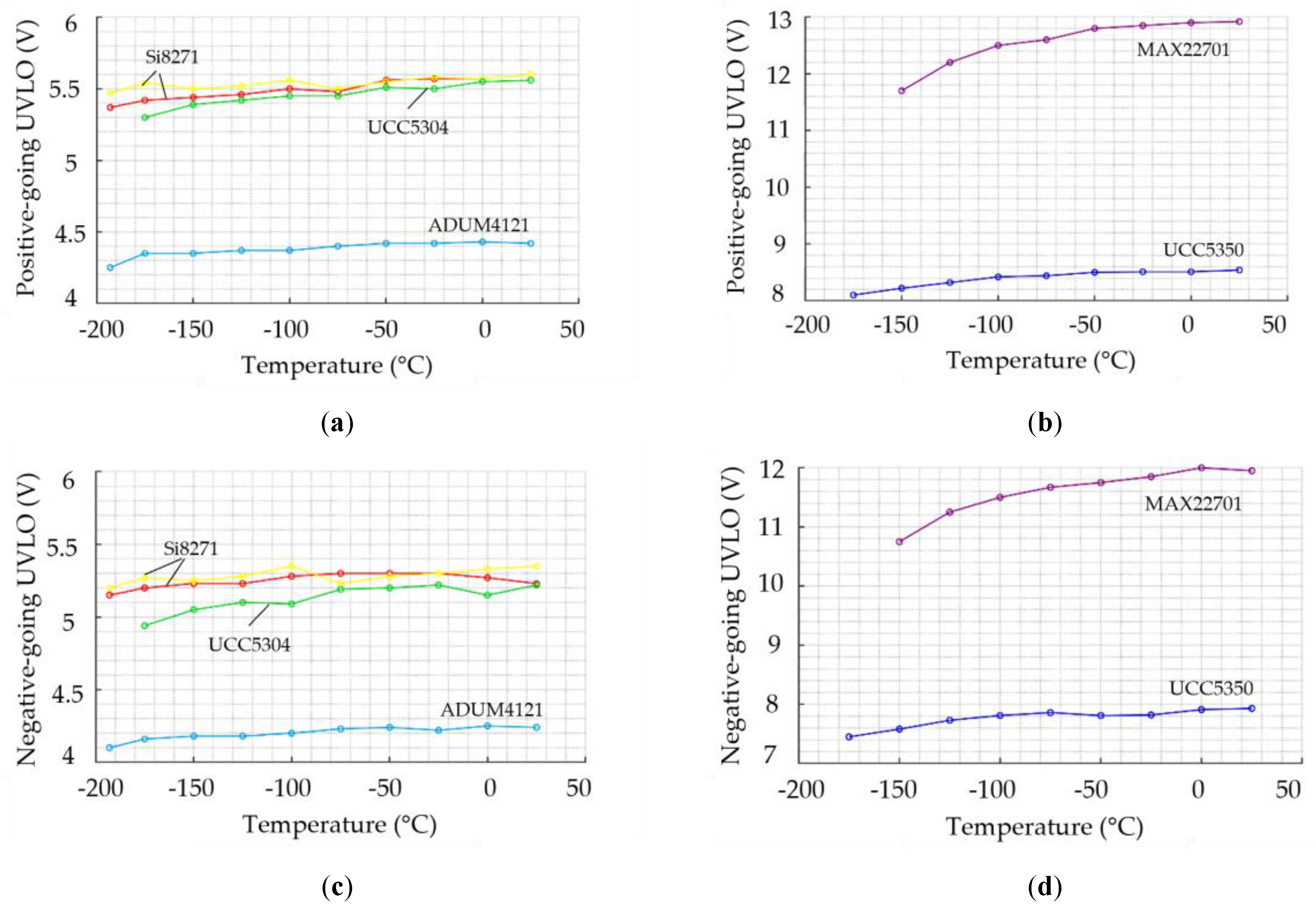
Figure 16.
Positive-going (a,b) and negative-going (c,d) UVLO threshold of half bridge drivers over temperature (marker: “o” High Side, “x” Low Side).
Figure 16.
Positive-going (a,b) and negative-going (c,d) UVLO threshold of half bridge drivers over temperature (marker: “o” High Side, “x” Low Side).
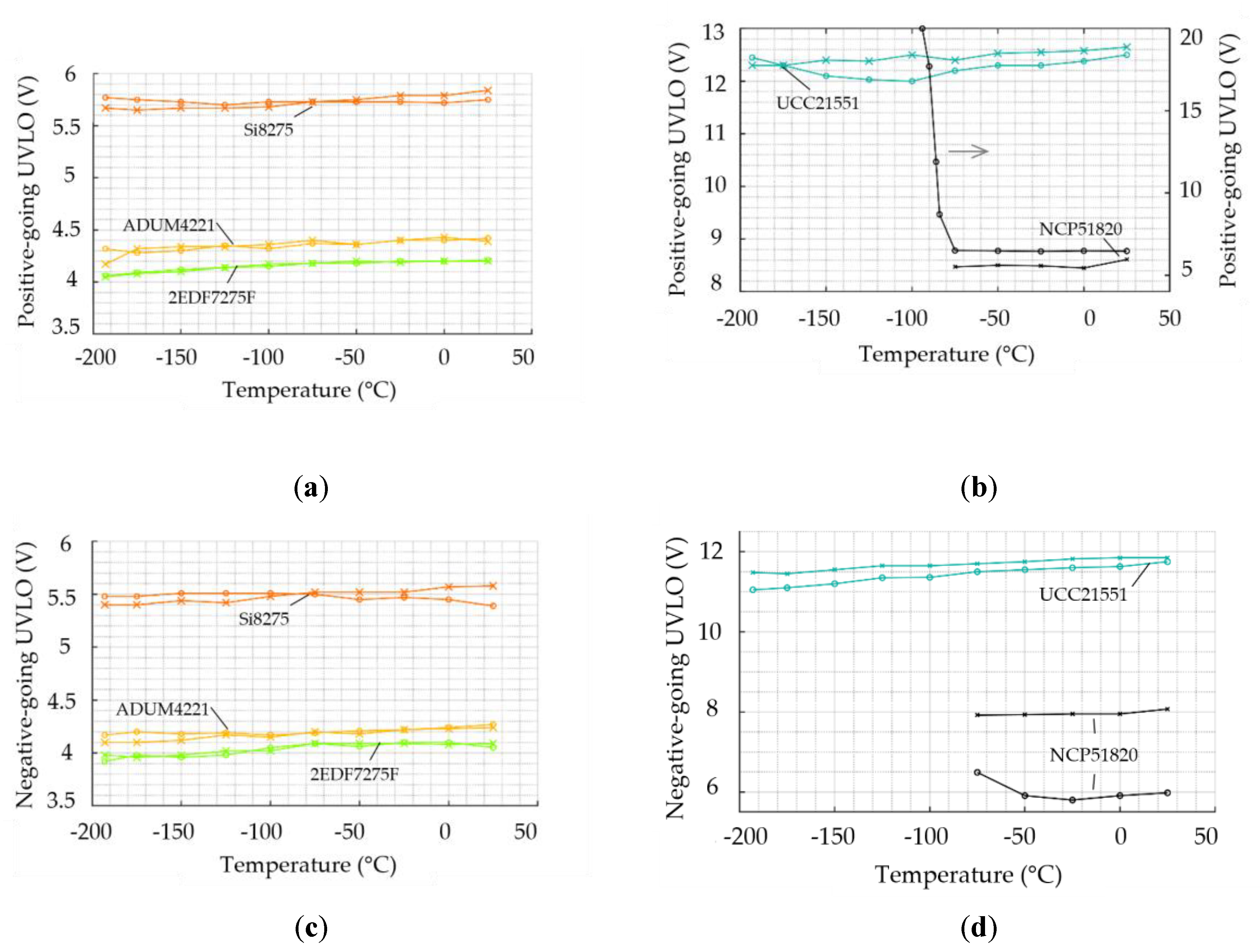
All drivers, except the NCP51820, show a slight, in case of the MAX22701 a more pronounced, de crease in the UVLO thresholds as the tem pe rature decreas es. Overall, however, the UVLO thres holds of all incon spic uous drivers are found to be remark ably stable. Nevertheless, from an application engineering point of view, a slight increase in the UVLO threshold values as the temperature decreases, corres pond ing to the increase in the threshold voltage of the power components, would be desirable.
The half-bridge driver NCP51820 is based on level shifter technology and the only tested device without galvanic iso lation. This device was included because it is specifically announced as a driver designed to meet the requirements for GaN transistors and therefore could be attractive for cryo genic GaN applications. Unfortunately, the driver failed at liquid nitrogen temperatures. As can be seen from Figure 16 (b), the problem is probably due to the UVLO threshold running away below -75 °C. At -95 °C, the UVLO threshold already exceeds the maximum driver supply voltage.
The two drivers Si8271AB and Si8271ABD behave simi lar ly regarding their UVLO behavior (s. Figures 13 (a/b) and 15 (a/c)). The designation "D" in the name stands for a "de glitch" variant. However, the tests did not reveal any influence of this variant on the UVLO behavior.
4.4. Common Mode Transient Immunity
A high CMTI (Common Mode Transient Immunity) is crucial for isolating gate drivers, especially when used to operate modern fast switching power semiconductors. It is essential that the driver's CMTI value exceeds the maximum voltage gradients on the floating power transistor. When using cryogenic power electronics, the CMTI requirements even increase due to the higher switching speed of GaN and Si FET at lower temperatures. As measurement results indicate, the speed of GaN-HEMT at cryogenic temperatures can nearly double from 70 V/ns to 130 V/ns compared to its performance at room temperature [13]. Modern drivers such as Si827x or MAX22701 are specified with a CMTI of up to 300 V/ns.
Since only output pulses from the CMTI tests are presented in the following figures, one detailed measurement result illustrating the evaluation of the CMTI behavior is shown in Figure 17 using the ADUM4121-1ARIZ. Beside the driver input voltage at room temperature and at -194 °C, this figure shows the burst voltage (vHV) as well as the driver output signal during one burst period. In later figures only the burst signal and the output signal are shown. Please note: Since in the present test setup the reference potential of the burst generator is at the output of the drivers (see Figure 4), positive voltage pulses cause a negative dv/dt at the rising edge according to the usual definition related to the primary side.
During burst measurements with voltages up to 2500 V, significant noise superimposes the measured output voltage as shown in Figure 18. With extensive investigations (short-circuited probes, etc.) we were able to verify that this noise is caused by interference coupled into the measurement setup and is not present in the output signal.
In order to improve the interpretation of the results with regard to possible faulty switching states, a low-pass filter with a sufficiently high cutoff frequency was used to attenuate the very high ringing frequencies. Depending on the CMTI value specified in the data sheet, tests were carried out at each temperature level with burst voltages between 1 kV and 2.5 kV. With a rise/fall time of the burst pulses in the range of 5 to 7 ns this results in voltage transients dv/dt in the range of 100 V/ns up to 350 V/ns.
Before discussing some drivers in detail, the following findings of the CMTI measurements can be summarized:
- Within the specified CMTI value, the following drivers showed no irregularities over the entire temperature range from room temperature to -194 °C (comparable to Figure 17): Si8271AB/D, 2EDF7275F, ADUM4121, ADUM4221, UCC5350 and UCC5304 (for the latter two, see also the mentioned parameter scatter with respect to the low-temperature functional limits)
- For the MAX22701, a short-term shutdown of the output signal was observed also at 0 °C and +100 V/ns, i.e. within the specified CMTI range (typ. 300 V/ns), see Figure 21.
- With decreasing temperature, and transient voltages exceeding the specified CMTI, some drivers tend to higher voltage drops, temporary OFF states, or even driver damage: UCC5304, UCC5350 and UC21551.
While all other drivers tested were unremarkable at room temperature, the half-bridge driver Si8275 showed a conspicuous error pattern: Specified in the datasheet as “min. 200 V/ns, max. 400 V/ns”, the driver behaved correctly at 250 V/ns during positive transients, but a strange malfunction was observed during negative transients (see Figure 19).
Depending on the burst amplitude, this ranged from a brief deactivation of the HS and LS output signals within a single signal period (e.g. 130 V/ns at -1.4 kV burst, see Figure 20) to a complete interruption of the output signals for a significant period after a burst event. For instance, at -0.5 kV, the output signal was interrupted for 220 ms, while at -1.1 kV, as illustrated in Figure 19, the interruption was significantly reduced to 3.3 ms. Due to the long measurement time, both the input and output signal can only be seen as colored areas and no longer as pulses. The output signal automatically resumed following this interruption, this applies to both the high-side (HS) and low-side (LS) outputs. Measurements conducted with replacement drivers from two different production batches, 2021 and 2024, showed consistent behavior. At negative transients exceeding 120 V/ns, malfunctions characterized by brief output deactivation were consistently observed across the entire temperature range down to -194 °C.
Within the typical CMTI specification, some drivers showed correct functioning across the entire temperature range from room temperature to -194 °C, under both negative and positive dv/dt conditions: This applies to the following drivers and the corresponding applied transient voltages: Si8271AB/D (±300 V/ns), 2EDF7275F (±300 V/ns), ADUM4121 (±200 V/ns), ADUM4221 (±170 V/ns), UCC5350 (±140 V/ns) and UCC5304 (±140 V/ns).
The CMTI behavior of the MAX22701 driver differed from that of the previously mentioned drivers. Within its specified typical CMTI of 300 V/ns, short-term deactivation of the output signal was already observed at 0 °C and positive transients with 100 V/ns, as illustrated in Figure 21 at 12 µs. At -150 °C, undefined output pulses occurred, and even after warming up to room temperature, the driver remained non-functional.
In general, interference on the driver output signal could be observed at high dv/dt values that approached or exceeded the specified maximum value. These were typically incomplete turn-on or turn-off operations with a duration of up to several hundred nanoseconds which is shown in Figure 22 as an example. At -194 °C, the Si8271 showed short turn-off events at positive transients of 350 V/ns, while at negative transients of the same steepness no false ON/OFF states were observed over the entire temperature range.
Some drivers showed permanent damage when the maximum specified dv/dt was exceeded, despite careful care not to exceed the maximum specified voltage amplitude. The UCC5304, e.g., showed irregularities at the output at -150 °C and +100 V/ns, after voltage transients of up to ±300 V/ns were applied at each temperature level during the cooling process (s. Figure 23). When the device was stressed exclusively with transients within the specification of ±130 V/ns, no irregularities were observed across the entire temperature range.
A similar behavior was observed with the UCC5350 (rated at typ. 120 V/ns). Starting at room temperature with transients exceeding 200 V/ns, no more output pulses were detected at -150 °C, and functionality did not recover upon reheating to room temperature. After replacing the driver and limiting the transient voltage to ±130 V/ns at each temperature level, proper functionality was maintained down to -194 °C.
The UCC21551 with a dv/dt rating >125 V/ns exhibited a similar behavior too. At -100 °C and +170 V/ns, missing and shortened pulses were detected, as shown in Figure 24. When voltage transients of up to ±200 V/ns were applied to the driver at each temperature level, no output signal was produced at -125 °C and below. CMTI measurements with approx. ±70 V/ns over the entire temperature range did not show any effects on the output signal.
5. Conclusions
This article presents a comprehensive characterization of isolated single- and half-bridge gate drivers across a temperature range extending from room temperature to cryogenic conditions. The measurement setup and characterization methodologies are described in detail, with particular emphasis on the measurement environment at low temperatures. All drivers were evaluated over the full temperature span, from room temperature down to -194 °C, focusing on rise/fall times, propagation delay, as well as undervoltage lockout (UVLO) and common-mode transient immunity (CMTI) performance.
Most of the tested drivers deliver a stable output signal for applications operating down to -194 °C. For operation above -150 °C, the MAX22701 represents a viable option, whereas the NCP51820 can be effectively used at temperatures down -75 °C. The UCC5350 and UCC5304 demonstrate deviations in output behavior at temperatures below -175 °C, with no output signal observed at -194 °C. Notably, other drivers from the same production batch, used for CMTI measurements, remained fully operational at -194 °C, suggesting potential variability in device performance under cryogenic conditions.
In general, rise and fall times remain within a narrow range, with a tendency toward shorter times at lower temperatures. However, at very low temperatures, some drivers exhibit an inverse trend. Contrary to the typical behavior of decreasing propagation delays with lower temperatures, the UCC5350 and UCC21551 show an increasing delay, while the MAX22701 experiences a sharp rise in propagation delay below -100 °C.
The first comprehensive characterization of power-up and power-down behavior in gate drivers has identified key operational characteristics relevant for practical applications. With the exception of the NCP51820, all tested drivers exhibit remarkably stable UVLO thresholds across their entire functional temperature range. Certain drivers—such as the UCCx series, MAX22701, and 2EDF7275F—stand out due to their particularly low output voltage levels in the low supply voltage range. However, it is important to note that, particularly in low or zero supply voltage conditions, none of the tested drivers is capable of actively pulling the output to zero. This effect becomes more pronounced in applications where Miller current induces a voltage drop across the chip’s internal gate resistance, potentially causing the gate voltage of a power transistor to exceed its threshold voltage, even in the absence of an external gate resistor. The challenge is further enhanced when utilizing GaN transistors, which feature significantly lower threshold voltages compared to Si-MOSFETs.
Regarding CMTI performance, several drivers maintained proper functionality across the entire temperature range from room temperature down to -194 °C, under both positive and negative dv/dt conditions, staying within their specified CMTI limits. This applies to the following drivers and their respective transient voltage ratings: Si8271AB/D (±300 V/ns), 2EDF7275F (±300 V/ns), ADuM4121 (±200 V/ns), ADuM4221 (±170 V/ns), UCC5350 (±140 V/ns) and UCC5304 (±140 V/ns).
At lower temperatures and transient voltages approaching or exceeding the specified CMTI limits, some drivers exhibited anomalies, including unintended switching events or potential decvice degradation. However, for applications such as drive converters, where switching speeds (dV/dt) are inherently limited, all the drivers mentioned in the previous paragraph can be used at temperatures down to -194 °C. For applications requiring extremely fast switching, drivers with particularly high CMTI robustness should be selected, such as the Si8271AB/D and 2EDF7275F, both rated at 300 V/ns.
References
- H. Gui et al. Review of Power Electronics Components at Cryogenic Temperatures. IEEE Transactions on Power Electronics 2020, 35, 5144–5156. [Google Scholar] [CrossRef] [PubMed]
- M. U. Hassan, Y. M. U. Hassan, Y. Wu, F. Luo, and V. Solovyov, "Development of Gate Drive Configuration for GaN Based Cryogenic Power Electronics Converters. in pp. 7039–7051.
- Kristen Boomer and Ahmad Hammoud, "Performance Evaluation of Isolated Gate Driver, ADuM4121, Under Exposure to Extreme Temperature.
- lpukach, "Extended Temperature Operation of Isolated, Precision Gate Driver, ADuM4120.
- J. Garrett, R. J. Garrett, R. Schupbach, A. B. Lostetter, and H. A. Mantooth, "Development of a DC Motor Drive for Extreme Cold Environments. in 2007 IEEE Aerospace Conference, 2007, pp. 1–12.
- Mustafeez–ul–Hassan, Y. Wu, V. Solovyov, and F. Luo, "Liquid Nitrogen Immersed and Noise Tolerant Gate Driver for Cryogenically Cooled Power Electronics Applications. in 2022 IEEE Applied Power Electronics Conference and Exposition (APEC), 2022, pp. 555–561.
- Y. Wei, M. M. Y. Wei, M. M. Hossain, R. Sweeting, and A. Mantooth, "Functionality and Performance Evaluation of Gate Drivers under Cryogenic Temperature. in 2021 IEEE Aerospace Conference (50100), 2021, pp. 1–9.
- D. Conway Lamb et al. An FPGA-based instrumentation platform for use at deep cryogenic temperatures. The Review of scientific instruments 2016, 87, 14701. [Google Scholar] [CrossRef] [PubMed]
- Y. Liao et al. Review of semiconductor devices and other power electronics components at cryogenic temperature. iEnergy 2024, 3, 95–107. [Google Scholar] [CrossRef]
- L. Nela, N. Perera, C. Erine, and E. Matioli, "Performance of GaN Power Devices for Cryogenic Applications Down to 4.2 K. IEEE Transactions on Power Electronics 2021, 36, 7412–7416. [Google Scholar] [CrossRef]
- S. Büttner, J. Windisch, and M. März, "Design and Operation of a Cost-Effective Cooling Chamber for Testing Power Electronics at Cryogenic Temperatures. IEEE Instrum. Meas. Mag. 2023, 26, 46–51. [Google Scholar] [CrossRef]
- K. K. Leong, "Utilising Power Devices Below 100 K to Achieve Ultra-low Power Losses. University of Warwick, 2011.
- R. Chen and F. F. Wang, "SiC and GaN Devices With Cryogenic Cooling. IEEE Open Journal of Power Electronics 2021, 2, 315–326. [Google Scholar] [CrossRef]
Figure 1.
Miller Effect caused by a positive dv⁄dt at the low-side transistor.
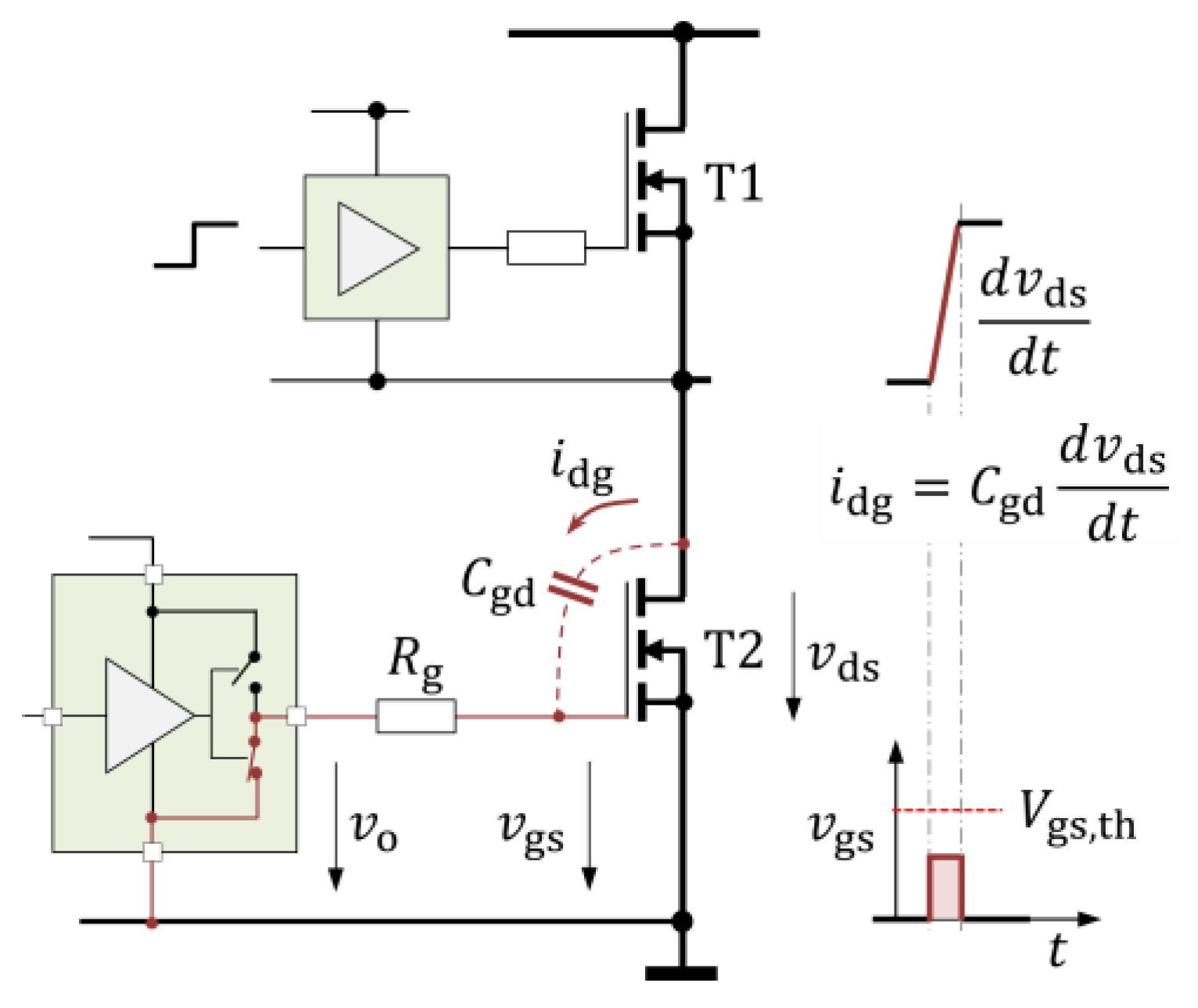
Figure 2.
Simplified schematic of test circuit used for single drivers.
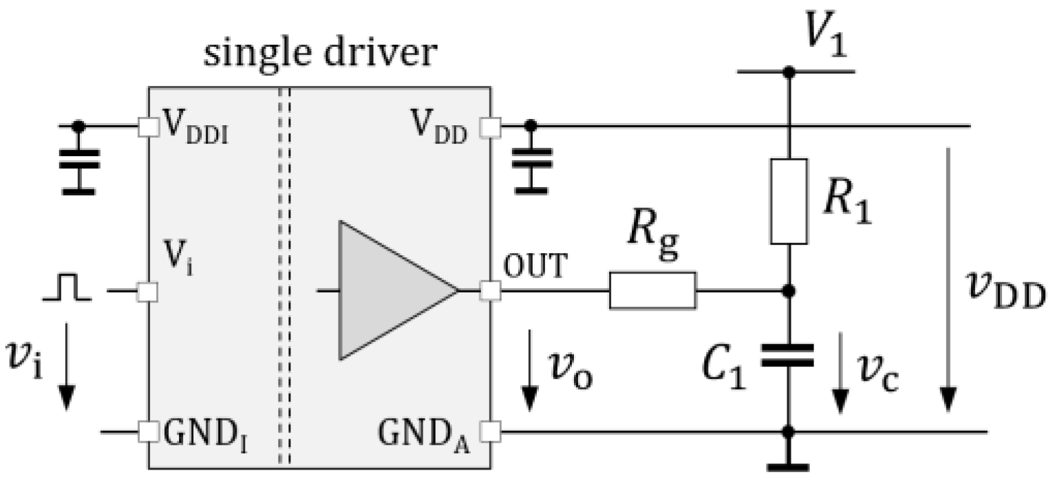
Figure 3.
Test method for positive- and negative-going undervoltage lockout (UVLO) threshold.

Figure 5.
Cryo test setup.
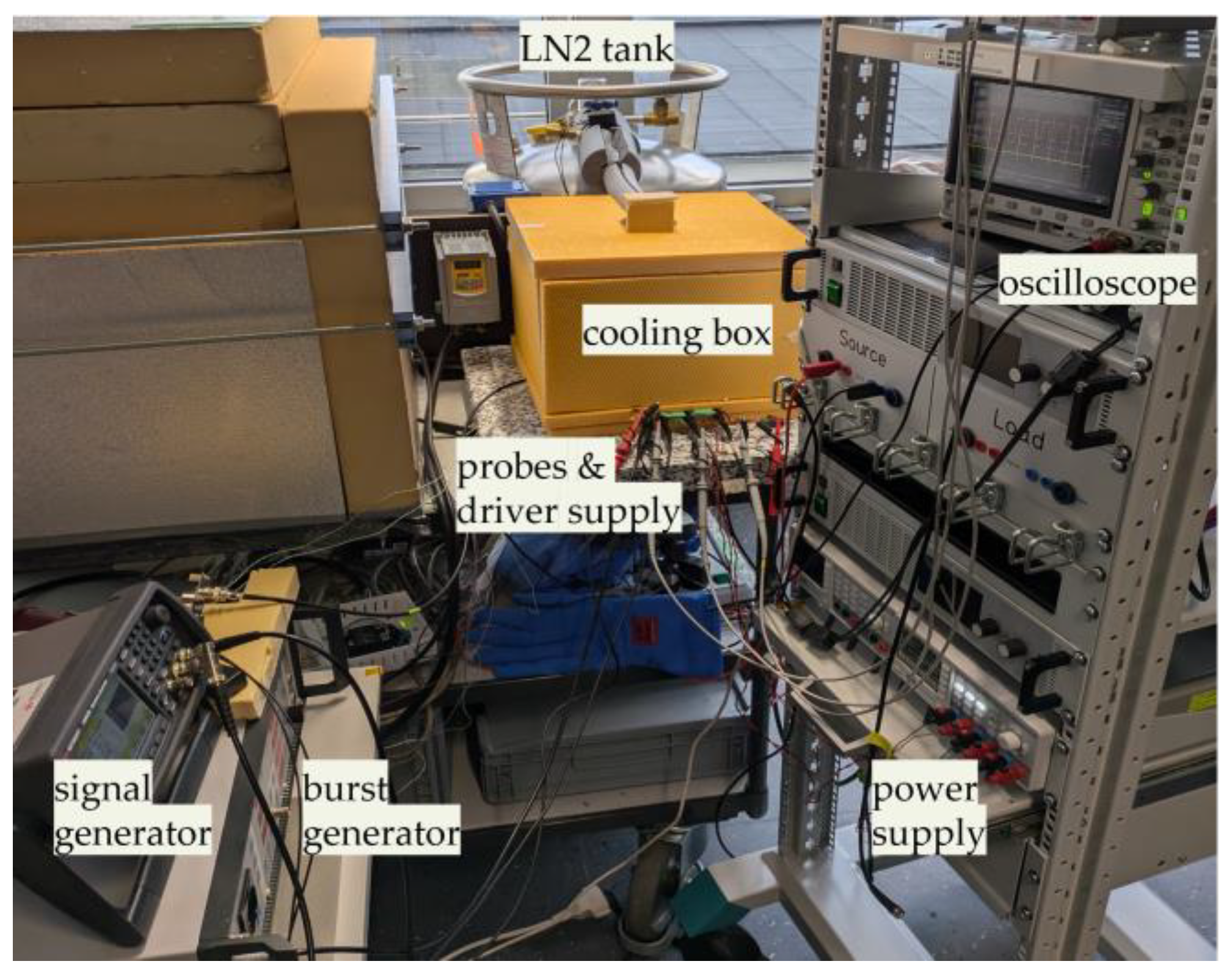
Figure 6.
Any temperature between -194 °C and room temperature can be applied to the DUT and kept constant with a tolerance of ±2 °C.
Figure 6.
Any temperature between -194 °C and room temperature can be applied to the DUT and kept constant with a tolerance of ±2 °C.
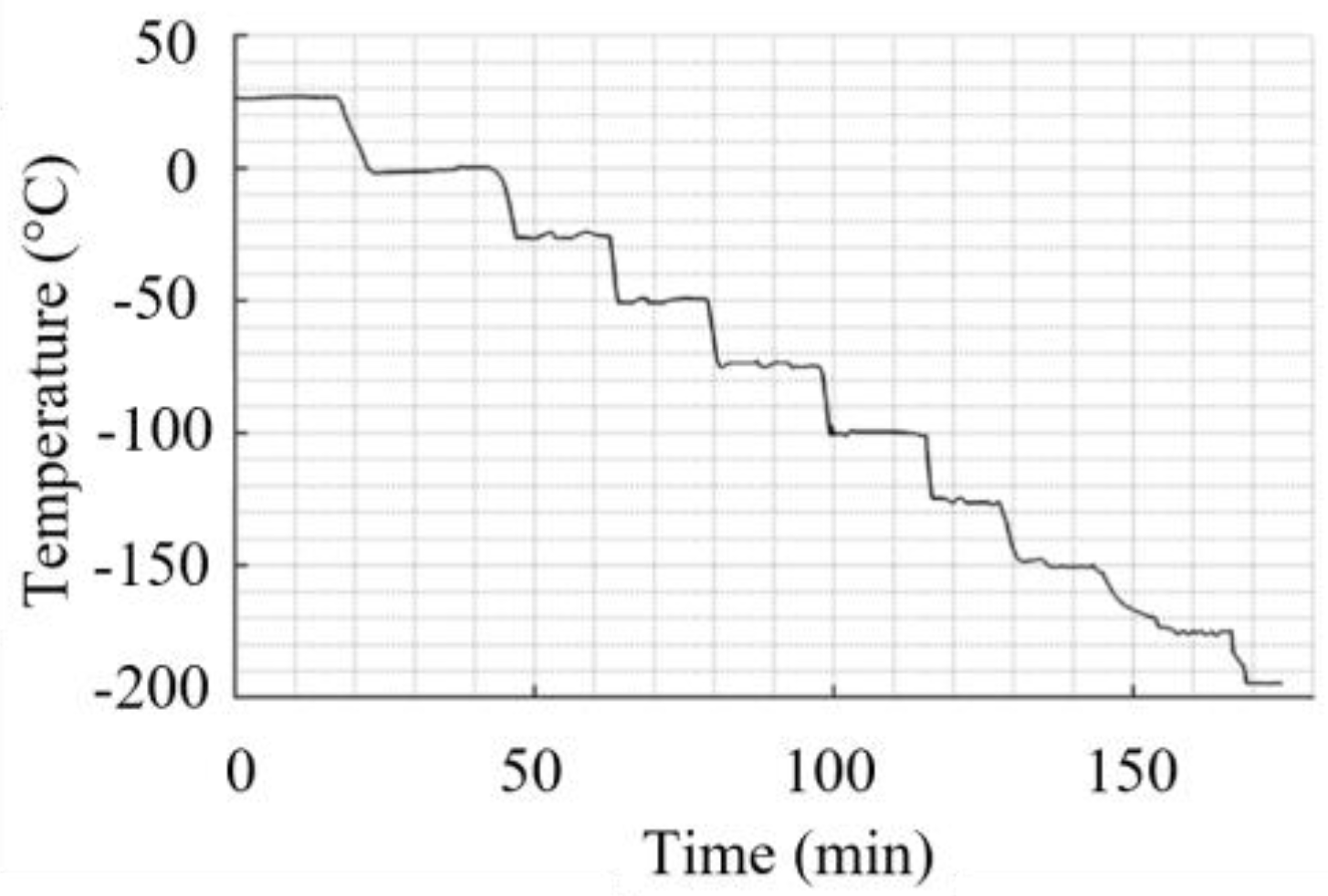
Figure 7.
Temperature-dependent output voltage (turn-on and turn off behavior) of Si8271ABD-IS.
Figure 8.
Rise time (a) and fall time (b) and the corresponding mean turn-on and turn-off currents over temperature for the tested single gate drivers; the magenta numbers on the right axis inside refer to the magenta curve (MAX22701) only.
Figure 8.
Rise time (a) and fall time (b) and the corresponding mean turn-on and turn-off currents over temperature for the tested single gate drivers; the magenta numbers on the right axis inside refer to the magenta curve (MAX22701) only.
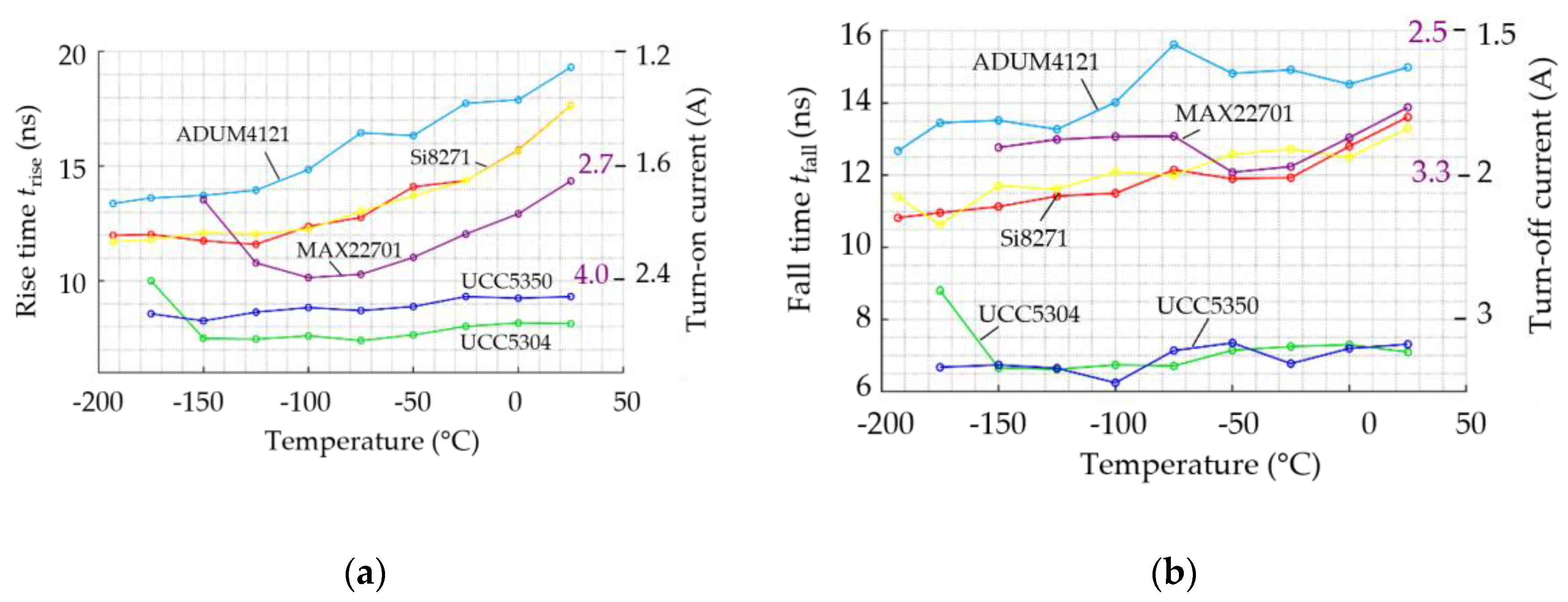
Figure 9.
Rise times (a) and fall times (b) over temperature for the high-side driver of the half bridge ICs; the cyan numbers on the right axis inside refer to the cyan curve (UCC21551) only. Without otherwise mentioned the low-side driver channel showed nearly identical temperature behavior.
Figure 9.
Rise times (a) and fall times (b) over temperature for the high-side driver of the half bridge ICs; the cyan numbers on the right axis inside refer to the cyan curve (UCC21551) only. Without otherwise mentioned the low-side driver channel showed nearly identical temperature behavior.
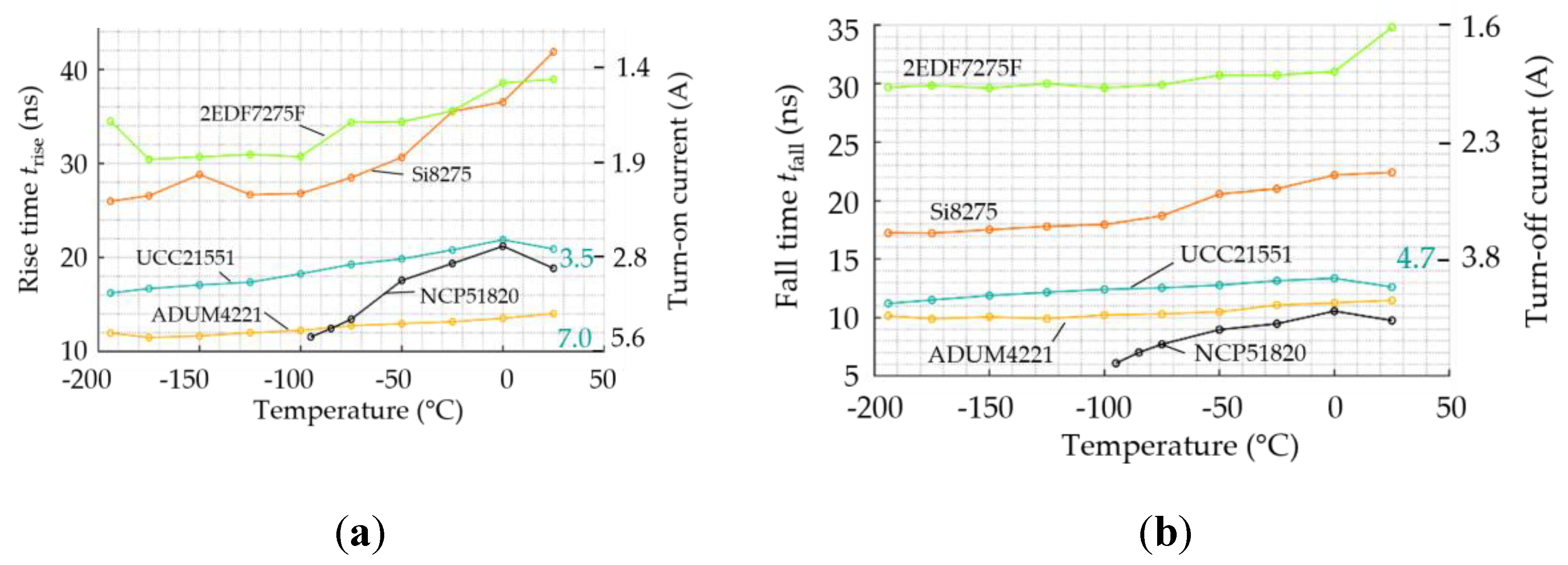
Figure 10.
Propagation delay: (a) “low-to-high” (turn-on) and (b) “high-to-low” (turn-off) over temperature for the single drivers.
Figure 10.
Propagation delay: (a) “low-to-high” (turn-on) and (b) “high-to-low” (turn-off) over temperature for the single drivers.
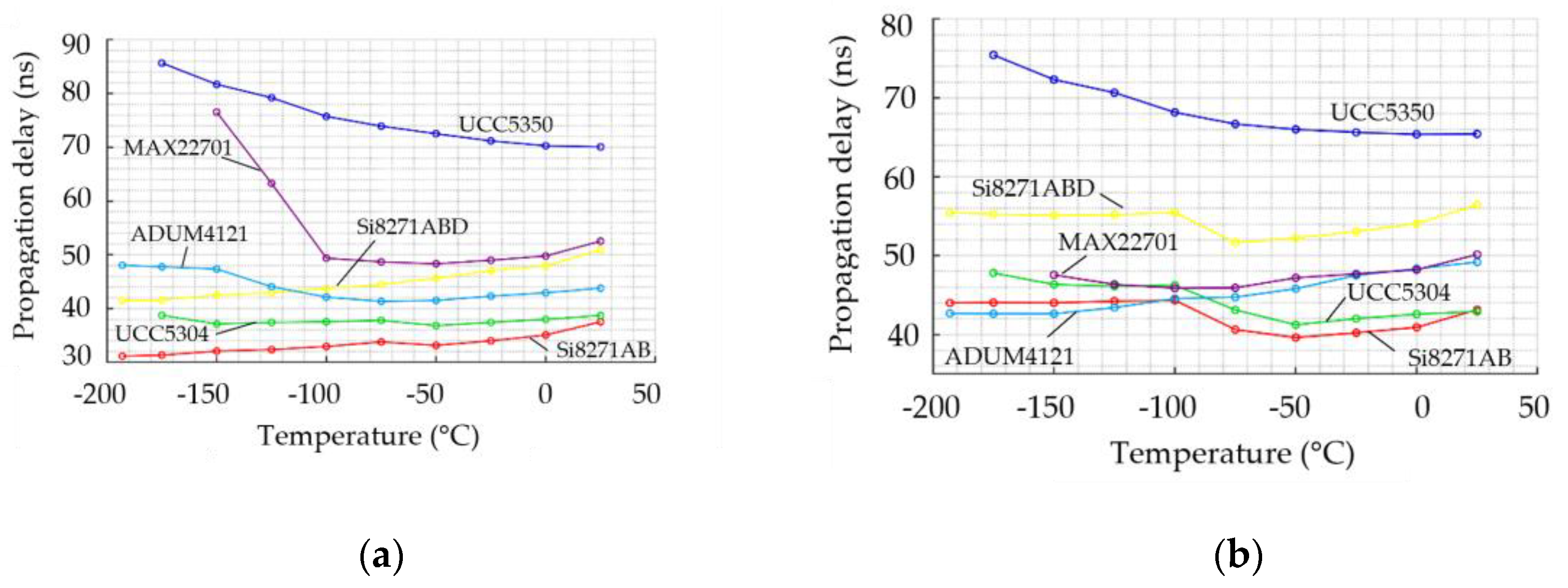
Figure 11.
Propagation delay “low-to-high” (a) and “high-to-low” (b) for high-side of the half bridge drivers over temperature; the low-side channel showed similar tempera ture behavior.
Figure 11.
Propagation delay “low-to-high” (a) and “high-to-low” (b) for high-side of the half bridge drivers over temperature; the low-side channel showed similar tempera ture behavior.
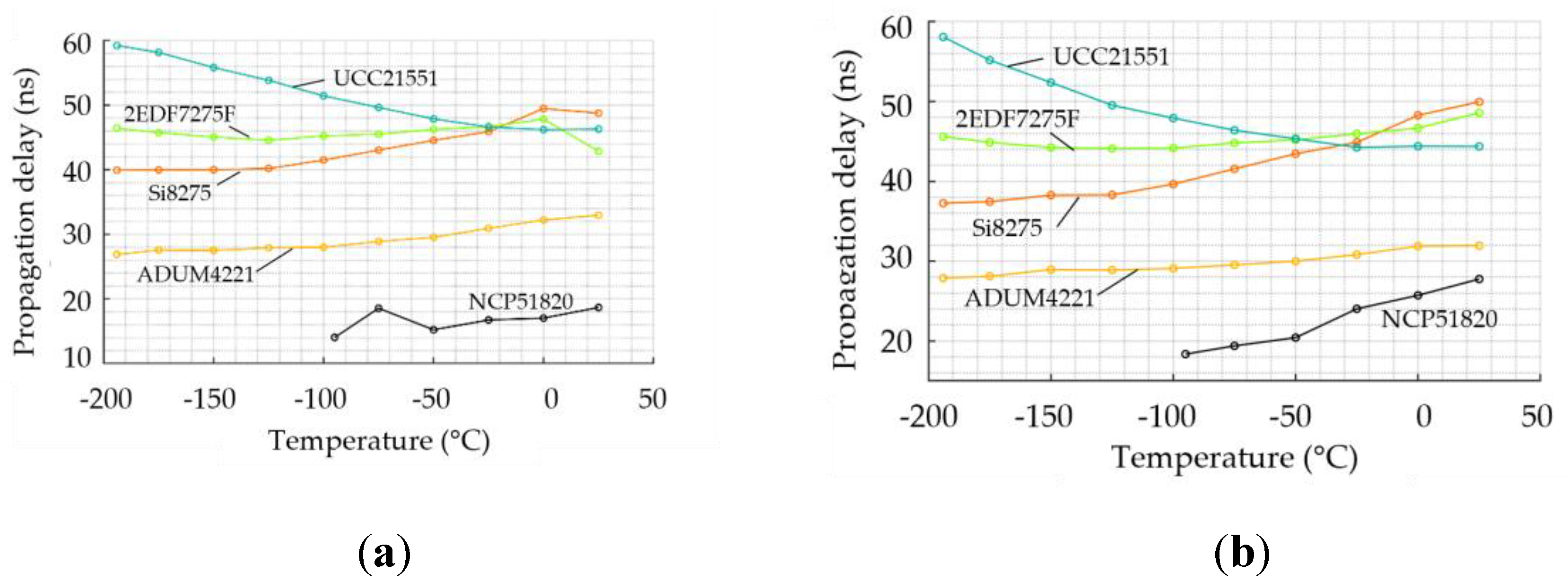
Figure 13.
Output voltage vo and driver supply voltage vDD for testing the positive- and negative-going UVLO threshold over temperature: (a) Si8271AB-IS; (b) Si8271ABD-IS; (c) ADUM4121-1ARIZ; (d) UCC5304-DWVR; (e) UCC5350SBD; (f) MAX22701EASA.
Figure 13.
Output voltage vo and driver supply voltage vDD for testing the positive- and negative-going UVLO threshold over temperature: (a) Si8271AB-IS; (b) Si8271ABD-IS; (c) ADUM4121-1ARIZ; (d) UCC5304-DWVR; (e) UCC5350SBD; (f) MAX22701EASA.
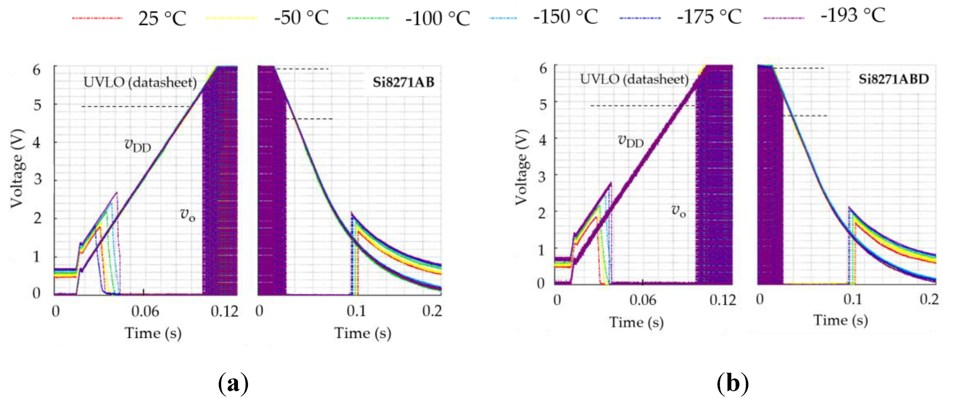

Figure 14.
High-side vo and driver supply voltage vDD for testing the positive- and negative-going UVLO threshold over temperature: (a) Si8275ABD-IS1; (b) ADUM4221-2; (c) 2EDF7275F; (d) UCC21551-Q1.
Figure 14.
High-side vo and driver supply voltage vDD for testing the positive- and negative-going UVLO threshold over temperature: (a) Si8275ABD-IS1; (b) ADUM4221-2; (c) 2EDF7275F; (d) UCC21551-Q1.
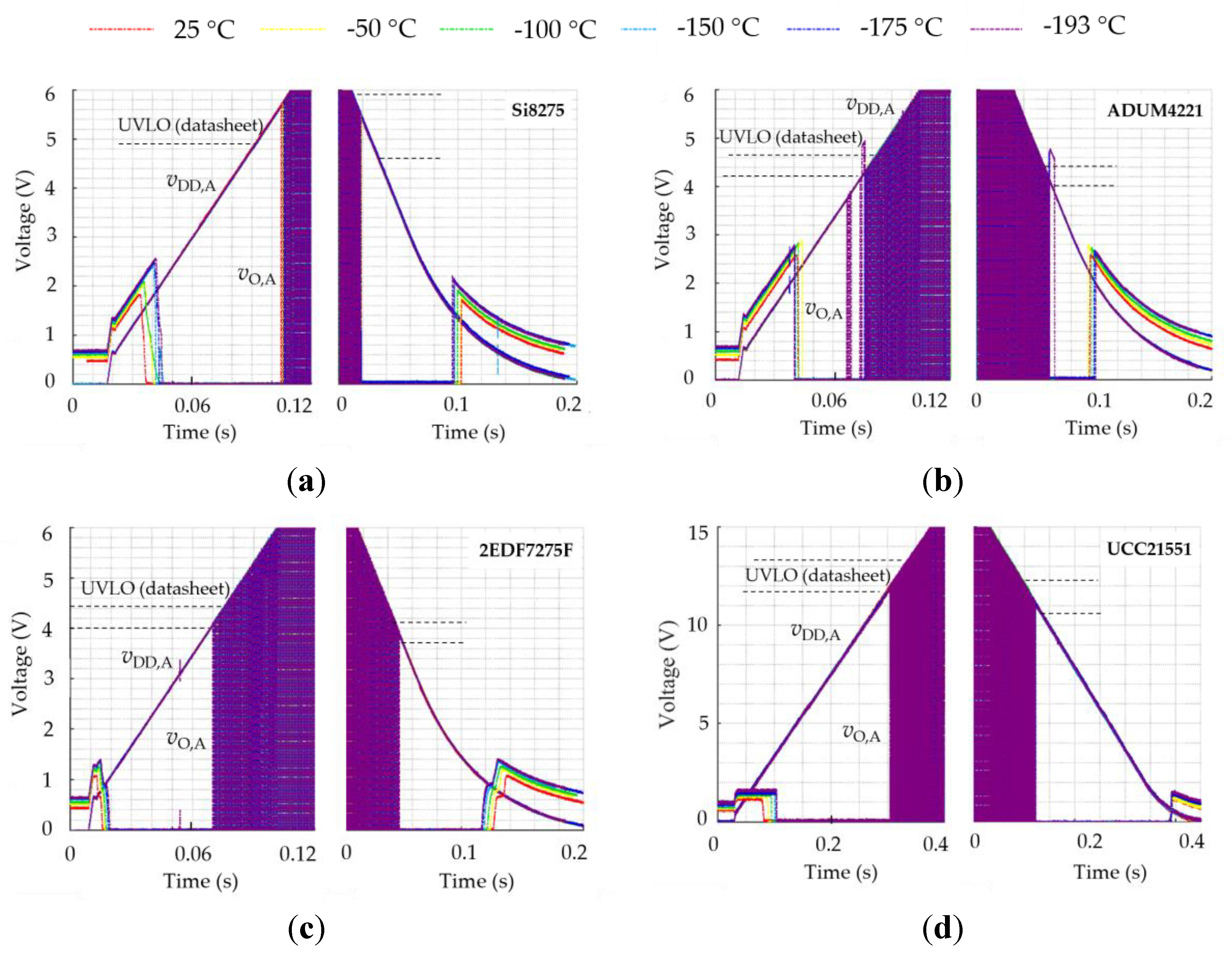
Figure 17.
Example for CMTI Test of ADUM4121-1ARIZ: Input voltage, burst-voltage and output voltage at 25 °C and -194 °C.
Figure 17.
Example for CMTI Test of ADUM4121-1ARIZ: Input voltage, burst-voltage and output voltage at 25 °C and -194 °C.
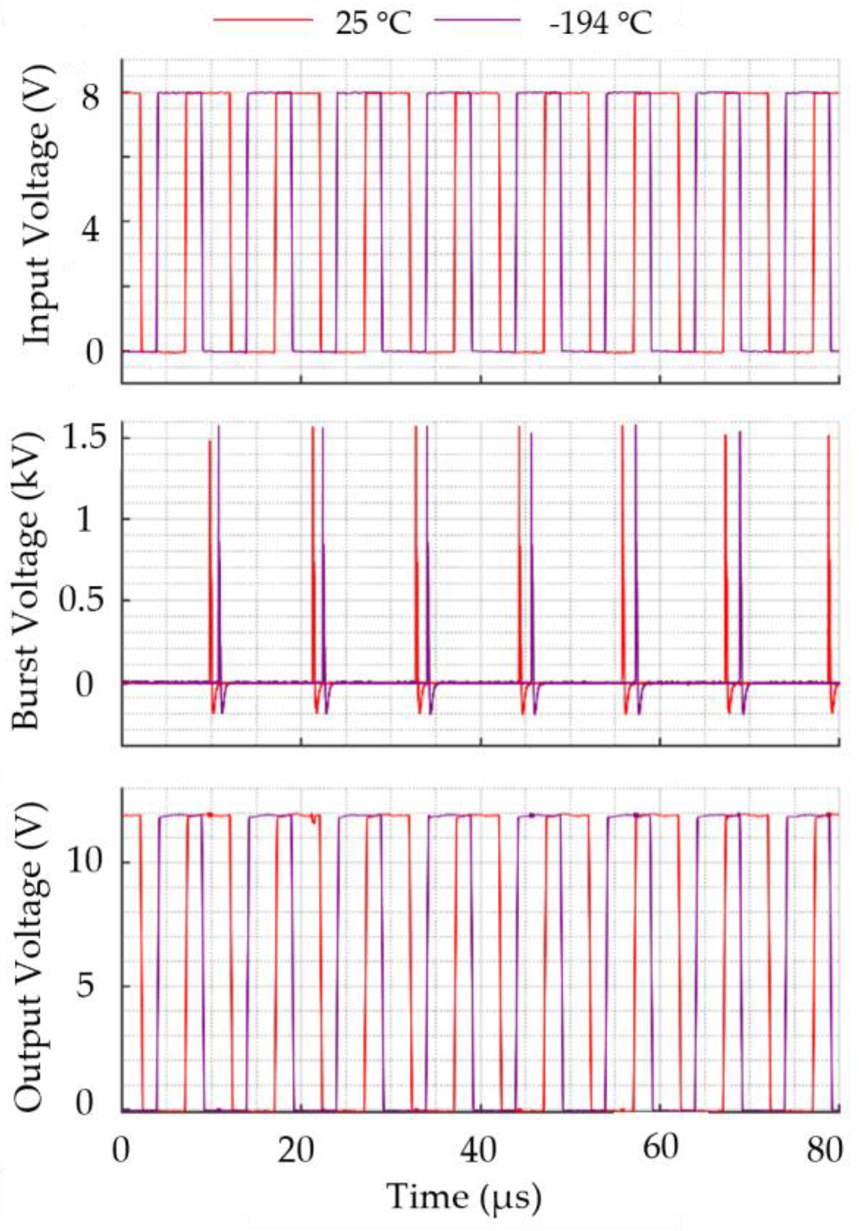
Figure 18.
Measured output voltage at ADUM4121-1ARIZ at 25 °C and -194 °C without (top) and with signal filtering (bottom).
Figure 18.
Measured output voltage at ADUM4121-1ARIZ at 25 °C and -194 °C without (top) and with signal filtering (bottom).
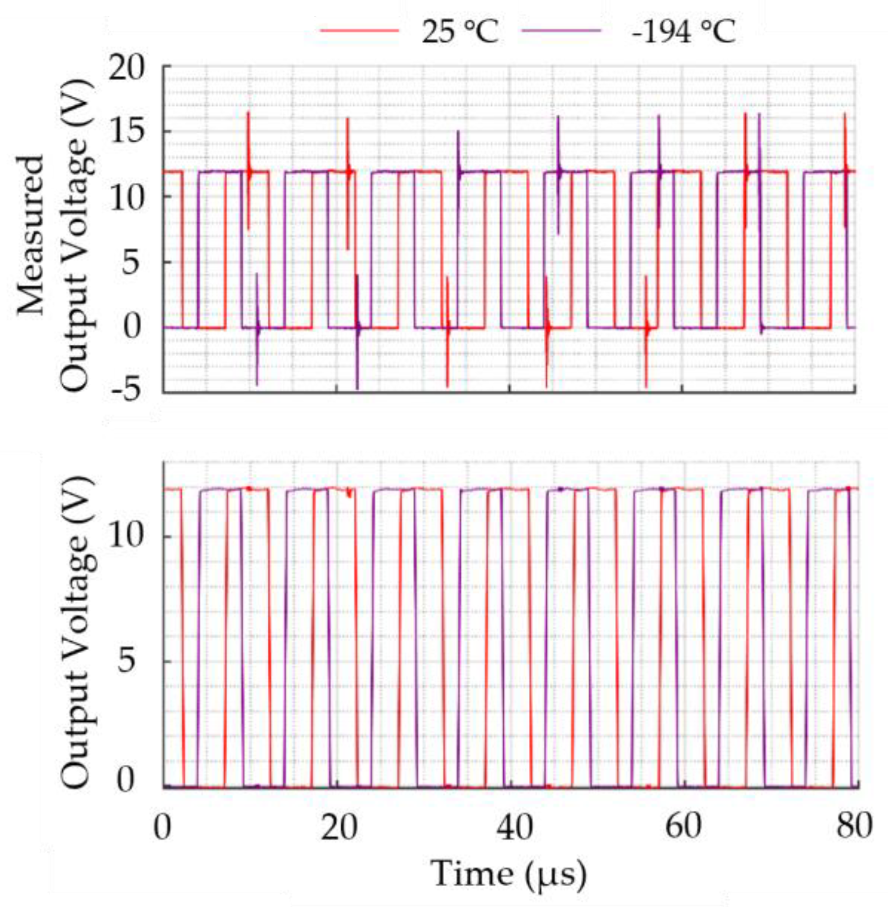
Figure 19.
CMTI Test of Si8275 with -1.1 kV burst voltage: input voltage (HS/LS), burst-voltage and output voltage (HS/LS) at 25 °C.
Figure 19.
CMTI Test of Si8275 with -1.1 kV burst voltage: input voltage (HS/LS), burst-voltage and output voltage (HS/LS) at 25 °C.
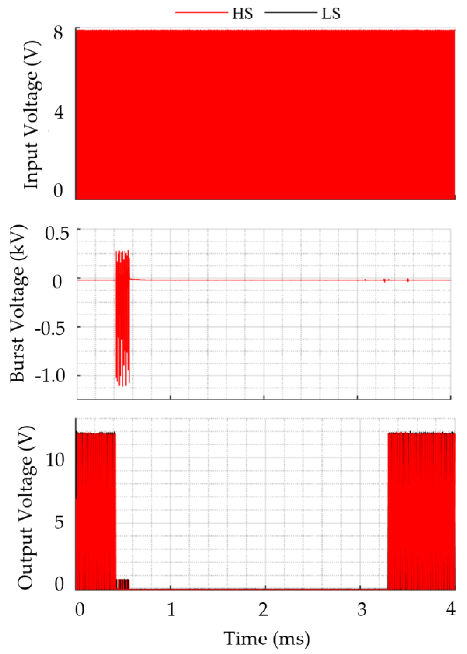
Figure 20.
CMTI Test of Si8275 with dV/dt = -130 V/ns: burst-voltage and output voltage (HS/LS) at 25 °C.
Figure 20.
CMTI Test of Si8275 with dV/dt = -130 V/ns: burst-voltage and output voltage (HS/LS) at 25 °C.

Figure 21.
CMTI Test of MAX22701 with +100 V/ns: burst-voltage and output voltage at 0 °C and -150 °C.
Figure 21.
CMTI Test of MAX22701 with +100 V/ns: burst-voltage and output voltage at 0 °C and -150 °C.
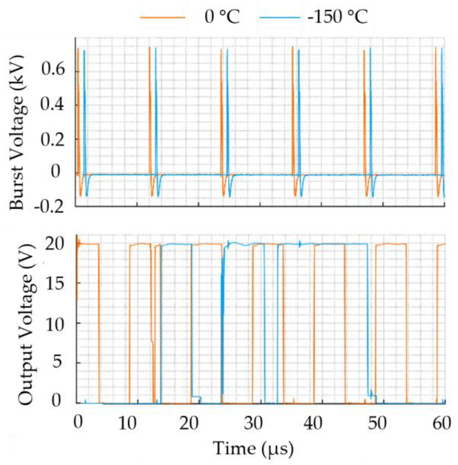
Figure 22.
CMTI Test of Si8271ABD with +350 V/ns: burst-voltage and output voltage at 25 °C and -194 °C.
Figure 22.
CMTI Test of Si8271ABD with +350 V/ns: burst-voltage and output voltage at 25 °C and -194 °C.
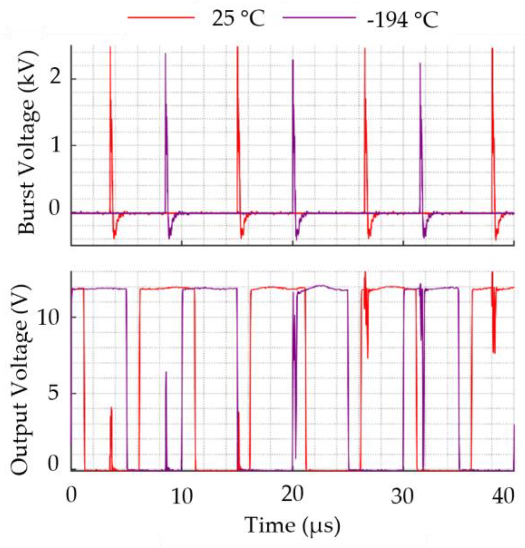
Figure 23.
CMTI Test of UCC5304 with +100 V/ns: burst-voltage and output voltage at 25 °C and -150 °C (after repeated ±300 V/ns).
Figure 23.
CMTI Test of UCC5304 with +100 V/ns: burst-voltage and output voltage at 25 °C and -150 °C (after repeated ±300 V/ns).
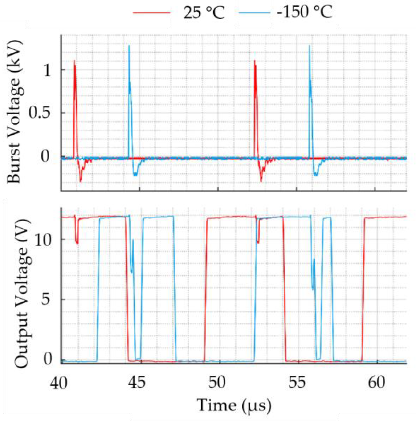
Figure 24.
CMTI Test of UCC21151 with +170 V/ns voltage: burst-voltage and high side output voltage at 25 °C, -50 °C and -100 °C.
Figure 24.
CMTI Test of UCC21151 with +170 V/ns voltage: burst-voltage and high side output voltage at 25 °C, -50 °C and -100 °C.


Table 1.
Investigated driver IC’S (S: Single driver, HB: half-bridge driver)
| Gate driver | Type | Color | Manufacturer | Galvan. Isolation |
VDD A/B | Ci, i=1,2,3 | Rg |
|---|---|---|---|---|---|---|---|
| Si8271AB-IS | S |  |
Skyworks Solutions Inc. | Semiconductor-based barrrier | 12 V | 2 nF | 0 Ω |
| Si8271ABD-IS | S |  |
Skyworks Solutions Inc. | Semiconductor-based barrrier | 12 V | 2 nF | 0 Ω |
| ADUM4121-1ARIZ | S |  |
Analog Devices Inc. | Inductive | 12 V | 2 nF | 3.9 Ω |
| UCC5304DWVR | S |  |
Texas Instruments | Capacitive | 12 V | 2 nF | 0 Ω |
| UCC5350SBD | S |  |
Texas Instruments | Capacitive | 12 V | 2 nF | 0 Ω |
| MAX22701EASA | S |  |
Analog Devices Inc. | Capacitive | 20 V | 2 nF | 0 Ω |
| Si8275ABD-IS1 | HB |  |
Skyworks Solutions Inc. | Semiconductor-based barrrier | 12 V | 4.7 nF | 0 Ω |
| ADUM4221-2 | HB |  |
Analog Devices Inc. | Inductive | 12 V | 4.7 nF | 0 Ω |
| 2EDF7275F | HB |  |
Infineon Technologies | Inductive | 12 V | 4.7 nF | 3 Ω |
| UCC21551-Q1 | HB |  |
Texas Instruments | Capacitive | 15 V | 4.7 nF | 0 Ω |
| NCP51820 | HB |  |
Onsemi | 12 V | 4.7 nF | 0 Ω |
Disclaimer/Publisher’s Note: The statements, opinions and data contained in all publications are solely those of the individual author(s) and contributor(s) and not of MDPI and/or the editor(s). MDPI and/or the editor(s) disclaim responsibility for any injury to people or property resulting from any ideas, methods, instructions or products referred to in the content. |
© 2025 by the authors. Licensee MDPI, Basel, Switzerland. This article is an open access article distributed under the terms and conditions of the Creative Commons Attribution (CC BY) license (http://creativecommons.org/licenses/by/4.0/).
Copyright: This open access article is published under a Creative Commons CC BY 4.0 license, which permit the free download, distribution, and reuse, provided that the author and preprint are cited in any reuse.


