
Submitted:
29 September 2024
Posted:
30 September 2024
You are already at the latest version
Abstract
This paper proposes a design for a platform-based Multi-phase Interleaved Synchronous Buck Converter (MISBC) using Silicon (Si) based Metal-Oxide-Semiconductor Field-Effect Transistors (MOSFETs). A custom platform was developed to compare the theoretical performance of a MISBC circuit simulated with Multisim and compared it with a prototype that was built at Western Sydney University. The work disclosed in this manuscript describes some steps adopted during the selection of each component and technical considerations taken during the design of the Printed Circuit Board (PCB). The platform designed has a maximum power output of 260 Watts, with a buck reduction of the nominal voltage from 97 Volts to 24 Volts at a maximum switching frequency of 50 kHz. This switching frequency is achieved with an open-loop circuit configuration coupled with synchronized signal generators, used to validate the dead band required between the activation of each MOSFET implemented in a half bridge configuration. A summary of the results based on the duty cycle required to achieve the buck voltage desired highlights the advantages of each operating mode of the MISBC circuit, where the theoretical performance is compared against the data acquired during functional evaluations of the prototype, allowing further interpretations towards the optimal control algorithm required to maximize the performance output of MISBC circuits.
Keywords:
DC-DC Converter
; Buck Converter
; Si MOSFET
; Power Electronics
; Circuit Design
1. Introduction
The utilization of DC-DC converters is a necessity across several Power Conversion Units (PCUs) [1,2], utilized in Electrical Vehicles (EV) [3,4,5], battery systems, Photovoltaic Systems (PV) [6,7,8,9], even in Hydrogen production through electrolysis with Proton Exchange Membrane (PEM) [10,11,12]. Although DC-DC converters are used in various applications, their operating principle is well established. They adjust the output voltage of a DC circuit to either a higher or lower level. There are several topologies used in DC-DC converters, and each topology delivers a distinct characteristic towards the circuit structure, architecture, and control.
This paper aims to implement a MISBC circuit into a platform with configurable hardware, allowing up to twelve configurations to be implemented. The design and performance analysis process are described in detail, showing which hardware considerations were taken during the development of the PCB. This platform is capable of having up to 97 VDC connected to the input circuit, while a target of 24 VDC is maintained on the output, delivering up to 260 W. With a 24 VDC output voltage, this platform can be connected to several industrial applications.
The MISBC circuit evaluated in this paper can be implemented in stationary or portable applications, where the energy source and load demands have a variable rate. Some of the applications are Electrical Vehicles (EV), solar optimizers and charge controllers, charge circuits for battery management systems and general DC industry.
The paper discusses the selection of MISBC as a topology, highlighting efficiency and dynamic operations, adapting the circuit topology to the load demands and application requirements. The utilized MISBC structure has two phases, which can be synchronized at the same phase angle or offset depending on the circuit characteristics desired.
A simplified circuit based on MISBC is simulated, to confirm the calculations utilized to define the input and output capacitance and line induction using a Spice model of the MOSFETs selected during the development of the PCBA. Additionally, this paper focuses on the topology used on the MISBC for control and power management. To achieve four PWM signals into the MISBC circuit, four signal generators were utilized to evaluate the open loop operation of the circuit.
A practical approach was considered during the development circuit, where calculations were applied to define theoretical losses and overall efficiency, which then were confirmed with the MISBC prototype platform. Several design considerations were defined based on industrial standards established by the International Electrotechnical Commission (IEC), ensuring the results acquired can be replicated while complying with international and regional certifications.
2. Related Work and Research Gap
The utilization of multi-phase interleaved buck converters has lately been deployed into PEM systems. Xiaoquang et al. [11] describe a multi-mode fault tolerant operation control strategy of multi-phase interleaved buck converter developed for hydrogen production, where a DC power network is converter and adjusted to match the voltage requirements of electrolyze systems. The author focused on the reliability and efficiency enhancements of the system where redundant modules are operating at various times. To achieve a reliable operation, the authors developed an auxiliary interface using a synchronous buck converter, supporting a multi-phase interleaved buck converter, with a traditional diode return for the negative feedback on the load connection.
A detailed description of the circuit is provided, where a Field-Programmable Gate Array (FPGA) is deployed to implement a Digital Signal Processing (DSP) interface with an Analogue to Digital Converter (ADC), a performance comparison based on ripple cancellation and power transmission has been proposed and disclosed in a simple matter. Despite the simplified conclusions summarizing certain features of the power output resulting from the circuit implementation, no efficiency curve has been disclosed, or detailed hardware definition was mentioned in the paper. Additionally, no clear explanation of the reasoning for using synchronous buck converter on the auxiliary circuit was made, since all losses caused by the diode return for the negative feedback on the load would increase the system efficiency.
Another example of implementing a multi-phase interleaved DC-DC converter into hydrogen systems is to be proposed by Xu-Feng et. Al. [10]. A high step-up multi-phase interleaved boost converter was designed to interface the power output of fuel cells into a DC power network. The author implemented an interleaved boost circuit to reduce the ripple at the power conversion line and implemented a soft-switching circuit to optimize the output voltage stability. The circuit and system are introduced with a detailed explanation of the topology and circuit implementation. Additional analysis was conducted across multiple frequency ranges, and an efficiency curve proportional to the boost coefficient applied to the circuit. However, no thermo-electric considerations were factored into the PCB design, and the temperature rise of the switching circuit was not recorded, obscuring potential thermal instabilities related to frequency variation. All mathematical considerations on the design were made based on the ideal components and ideal operation characteristics of the system.
Niraj Rana et al. [13], implemented two conventional buck-boost converters operating with interleaved topology and controlled with a Dragonfly Algorithm. The authors provided a detailed visualization of the Interleaved Buck-Boost Converter (IBBC), followed by a mathematical model of the circuit topology which combines all operating modes into a single transfer function, configuring the operating conditions of the system. The transfer function was defined based on the charge and discharge characteristics of the system established by the line capacitance and line inductance of the circuit.
The mathematical model was evaluated with prototype connected to a variable power supply and fixed resistive load. The algorithm utilized a triangular waveform to set a sample rate, which was then tracked and compared with the switching circuit to analyze delayed mismatch propagation on the circuit. The authors did not disclose the PCBA construction or the power characteristics in which the prototype was evaluated. The comparison utilized to evaluate the circuit was the Maximum Overshoot (Mp) combined with the rise and settling times of the switching circuit. However, since the power characteristics and PCBA construction characteristics were not disclosed, it is hard to address if the Mp improvement was directly consequent to the algorithm itself, instead of being a consequence of the test conditions in which the circuit was evaluated.
Ahmed Zakaria et al. [14], proposed a circuit hybrid interleaved DC-DC converter, based on Buck-Boost topologies designed for medium voltage applications. The authors explained the circuit topology which has the option of having a diode on the negative discharge cycle or operating a MOSFET to counter the diode conductivity losses while accelerating the switching circuit. Fundamental equations were reviewed during the circuit design, and compared with previous papers in which similar topologies were applied. A transfer function was defined combining all the operating topologies proposed by the circuit, which was then simulated in MATLAB.
Despite having results from simulations conducted with theoretical output power reaching 8 kW through the DC link rated to 300V, combining three DC-DC converters, initially coupled to an AC-DC connected to a Wind Turbine, the authors claim to have achieved 50% reduction in the DC-DC conversion. Although, no further analysis has been performed, to evaluate the practicality of the system through a prototype or a conceptualization analysis.
As mentioned previously, several applications require DC-DC converters. Applications that optimize efficiency and reliability, at times, adopt interleaved configurations. This paper aims to provide a generic power conversion block, which can be optimized based on the physical space, energy density, cost, and efficiency. Peng Zhang et. Al. [15] utilized the same approach when proposing an efficient optimization control method with the fast dynamic response for a multi-phase interleaved buck converter. The author presented a MISBC circuit and optimized the output performance of the circuit based on the load requirements. The authors presented an approach based on a fixed hardware platform where the MISBC circuit was designed and integrated the hardware into an external microcontroller. This paper describes the overall topology of the circuit but does not disclose any design criteria on the PCB or calculations used on the component selection.
Despite having two power switching circuits operating in interleaved configuration; the presented results are of the circuit efficiency with both circuits operating in-phase, sharing the load, but not operating in offset configuration. By doing this, the authors only showcase the circuit partially, shadowing some of the benefits of having a MISBC circuit.
Gourab Banerjee et. Al. [16] utilized multi-phase interleaved buck circuits without a synchronized control, clearly showing the advantages of having an interleaved circuit and achieving up to 500kHz because of an interleaved power switching circuit using Silicon Carbide (SiC) MOSFETs. Puneet Kaur et al. [17], on the other hand, achieved the same switching frequency with a GaN MOSFET, and compared the overall performance of their system with a Si based MOSFET. Both papers clearly described their simulations and presented their results acquired from a customize prototype. Although, none of the considerations taken during the development of the prototype were disclosed, such as the implementation of Snub or Anti-Parallel circuits to stabilize the control and switching lines.
Most research papers on the development of DC-DC converters highlight the steady state and ideal evaluation of the circuit through simulations or mathematical models, which are rarely compared with a prototype [3,18,19]. In this paper, a different approach is used by providing additional details on the PCB design and performs functional tests where the input voltage is altered across a wide voltage range.
This paper aims to share a MISBC circuit design implemented in a customizable platform, allowing several footprints of capacitors, inductors and MOSFETS to be used, depending on the designed configuration. Two pairs of half bridge gate drivers were utilized to interface the external control circuit consisting of a set of signal generators synchronized into the same reference circuit produced by the dsPIC controller.
Key features of the gate driver have been emphasized, including output control voltage and thermal management of the IC thermal relief vias, along with additional shielding and heat sink layers on the PCB, were used to enhance the switching characteristics of each gate driver, independent of the implemented topology. This improves circuit lifespan, current boost coefficient, and EMI performance. A wide range of voltage input has been tested, where the buck circuit regulates the input voltage from 30 to 97 VDC into a 24VDC output, with switching frequencies varying from 25 kHz to 50kHz.
The main objective of this paper is to evaluate the operational switching time of each MOSFET, resulting in a predictable dead time between the operation of the High Side and Low Side circuit. This analysis allows the optimization of the synchronization topology applied on the MISBC circuit by reducing the power loss generated by the body diode of the MOSFET and voltage overshooting characteristics of the control circuit. Additionally, the temperature rise is acquired from the switching circuit, validating the performance and stability of the prototype.
Prior to the prototype validation, the circuit structure is simulated to evaluate the circuit layout and topology. While setting a theoretical benchmark for the activation of each MOSFET. Both efficiency and switching characteristics acquired based on the simulations are verified with the MISBC circuit design into a platform-based prototype.
The dead time evaluation in synchronous power conversion circuits is commonly overseen by engineers, which fail to achieve the optimal performance of the DC-DC converter by lacking an optimization procedure of the circuit, inducing additional losses consequent of delay mismatch propagation and phase drift between the control circuit and MOSFET operation. To demonstrate the effectiveness of the MISBC optimization, a MOSFET IRF530N is used, showing that even a basic MOSFET can achieve efficiency rates above 95% at 50 kHz. This sets a performance benchmark for comparing more advanced MOSFETs based on SiC and GaN technologies.
3. Methodology
Several steps were adopted to ensure the optimal configuration of the MISBC circuit to present the research, design, and performance evaluation accurately. Firstly, the circuit structure was defined, which included external connections, an auxiliary circuit, and a power bus required on the MISBC circuit.
A distinct topology was adopted, which includes four operating modes. Each mode provides its operating characteristics, defined in conjunction with its own control timing diagram.
All challenges superseded during the design of the electrical schematic and layout of the printed circuit board were discussed and correlated to its optimization process.
To provide a comprehensive understanding of the MISBC circuit, the structure and topology are explained using a simplified circuit diagram, which illustrates the current flow at each stage of operation. The time diagram necessary for operation is also disclosed. A summary of the component selection process is provided, focusing on key characteristics of the MOSFET and gate driver.
A circuit simulation evaluates overall efficiency, output voltage ripple, and output voltage stability. Special attention is given to synchronization time and dead time during the simulation, establishing control benchmarks for prototype implementation. During the prototype design and evaluation, a dielectric isolation test is performed to ensure the PCB can withstand the operating conditions of the MISBC topology.
To analyze circuit overshoot, a direct comparison is made between the input signal at the PCB and the gate signal driving the MOSFET, assessing the quality of the PCB design and the effectiveness of the snubber and anti-parallel circuits. Finally, the overall efficiency curve, output voltage ripple, and temperature rise from the circuit are used to compare the simulated results with the prototype evaluation. The figure below outlines the methodology used for the design and performance analysis of the platform based MISBC circuit. Figure 1 presents the steps followed from the circuit structure to the circuit performance evaluation.
4. Circuit Structure and Topology
The prototype built for the platform base MISBC circuit was designed to integrate the control and power bus system with an auxiliary power circuit coupled with input and output voltage and current sensors. These circuits ensure that the MISBC can be monitored and connected to any supervisory platform directly or indirectly using a dsPIC controller through a serial communication protocol, converting the data from the MISBC circuit into analogue signals.
Schematic Diagram
Figure 2 depicts the schematic diagram utilized on the platform base MISBC circuit. Each block represents a crucial part of the system. All blocks with orange infill represent an external connection to MISBC power output. This connection is established with modular connectors capable of withstanding three times the nominal rating of the overvoltage and over current protection circuit, ensuring the connection will withstand any fault condition.
All blocks with blue infill represent the power bus of the MISBC circuit. These blocks will undergo simulation to ensure all capacitors and inductors are correctly rated and aligned with the MISBC circuit topology. These components are the primary focus of this paper.
The utilization of MISBC allows multiple topologies or operating modes to be implemented. Each topology has advantages and disadvantages in circuit operation and power output characteristics. It is important to explore each topology, allowing operational flexibility of the circuit across the entire system. This section will describe each topology’s operation and highlight the characteristics of implementing each topology into a DC-DC converter. Each topology will be represented with a simplified electrical diagram, each charge and discharge cycle are individually represented, and an additional timing diagram is also provided, where the Total Period (ts) is set as a baseline for the On-Time of the Low Switch MOSFET () and On-Time of the High Switch MOSFET ( to disclose the logic operation of the control circuit.
To assist in explaining the MISBC topology it is important to provide the nomenclature from each section of the circuit. Figure 3 depicts each section based on the simplified schematic used to explain the MISBC topology.
Buck Converter Operation
A conventional Buck converter utilizes a diode to discharge the energy stored at the line inductor. In a MISBC circuit, either the Buck Circuit A or Buck Circuit B can be used. During the charge and discharge cycle. In this operation, the MISBC circuit performs the same way as any other buck converter since the body diode of the Low Side MOSFET indicated as Q3 on the diagram discharges the inductor.
This operation allows a pre-charge circuit or a load with a high inrush current to operate without creating a short circuit path across the High Side and Low Side circuits countering any issues that might occur with the control circuit. Although, since the body diode of the Low MOSFET is used, additional power losses must be accounted for, impacting the overall efficiency of the circuit. Figure 4 highlights the charge and discharge cycles of a conventional buck converter and shows the timing diagram required for its operation.
Synchronous Buck Converter Operation
A synchronous buck operation uses the Low Side MOSFET to discharge the line inductor. Either Buck Circuit A or Buck Circuit B can be used during the charge and discharge cycle in the MISBC circuit. This circuit can be troublesome if the dead time between each MOSFET is not optimized or an unexpected propagation mismatch between the gate driver and MOSFET occurs. If calibrated and synchronized correctly, this topology can be very efficient, since it eliminates the losses of the diode required during the discharge cycle.
Figure 5.
(a) Charge cycle of a synchronous buck operation; (b) Discharge cycle of a synchronous buck operation; (c) Timing diagram required in a synchronous buck operation.
Figure 5.
(a) Charge cycle of a synchronous buck operation; (b) Discharge cycle of a synchronous buck operation; (c) Timing diagram required in a synchronous buck operation.
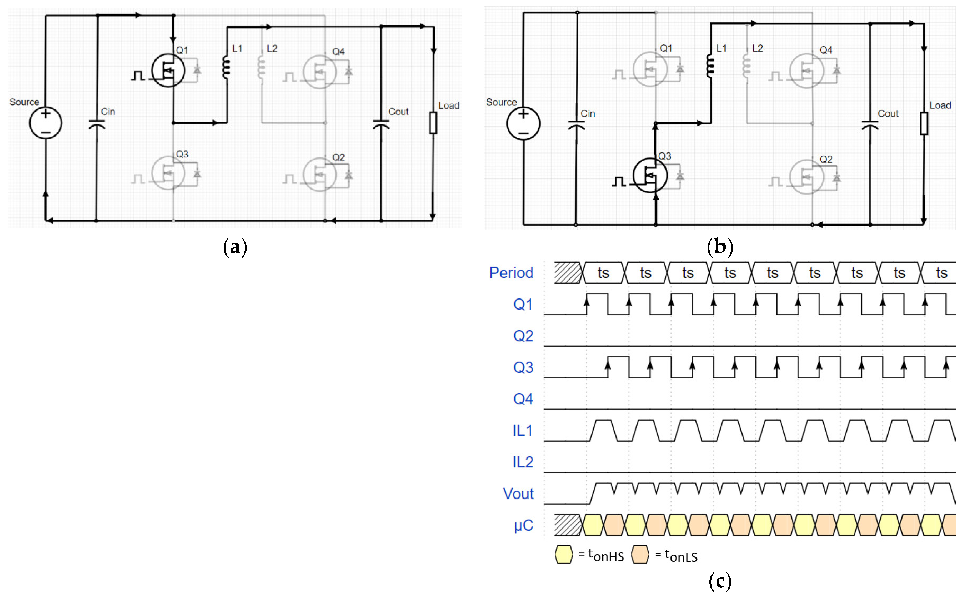
Interleaved Synchronous Buck Converter Operation
A synchronous interleaved operation is based on a synchronous buck operation while using the Low Side and High Side MOSFETs of both Buck Circuits. Each circuit is out of phase, with a 180° delay between each control circuit. Each circuit will be operating at half of the load frequency while maintaining the control circuit energized twice as long, doubling the duty cycle required, compared to a synchronous buck operation.
This operation has a great advantage towards power losses consequent of the switching frequency of each buck circuit. Although, the complexity of the control circuit is much greater than any other operation topology. This topology has the same optimization requirements as the synchronous buck converter. However, each circuit must be perfectly synchronized, otherwise permanent damage will occur to the switching circuit. Figure 6 depicts 4 combinations of analyzed synchronous buck converters.
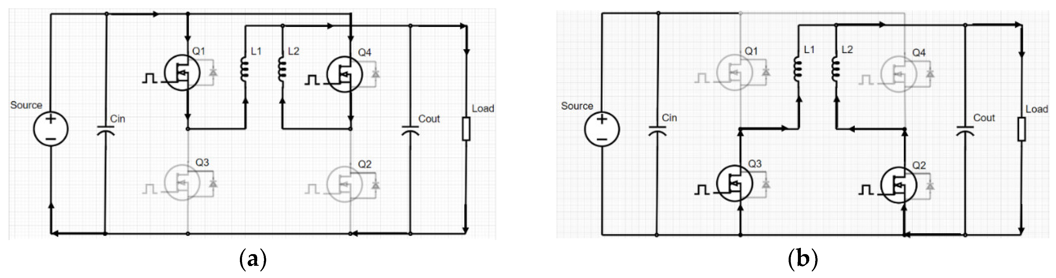
Parallel Operation Synchronous Buck Converter
A parallel operation is based on a synchronous buck operation. Both synchronous buck circuits are in phase, allowing a parallel operation. This topology is not only used to reduce losses, but it also allows the power output to double, without compromising the circuit structure. This topology has the same challenges as the synchronous buck converter.
Figure 7.
(a) Charge cycle of a parallel synchronous buck operation; (b) Discharge cycle of a parallel synchronous buck operation.
Figure 7.
(a) Charge cycle of a parallel synchronous buck operation; (b) Discharge cycle of a parallel synchronous buck operation.
5. Component Selection and Circuit Simulation
The component selection for MISBC is the first step towards the evaluation of the circuit design. The first component to be defined is the MOSFETs. As mentioned previously a Si based MOSFET was utilized for the circuit evaluation. The IRF530N is a commonly used MOSFET, which made its debut on the global market in 1999. Its technology is well established, and it is a device known as easy to source and reliable.
Table 1 shows some of the electrical characteristics of the MOSFETs utilized in this paper. Ratings such as Drain-to-Source Voltages (VDS) and Rated Drain Current (ID), are related to the system requirements. However, Drain-Source-On resistance (RDS (on)), Total Gate Charge (Qg) and Reverse Transfer Capacitance (CRSS) have a direct impact on the switching and operational losses of the MOSFET. It is also important to highlight the Maximum Temperature Junction (Tj (Max)), Junction-to-Ambient Thermal Resistance (RΘJA) and Nominal Power Dissipation (PD) impact the temperature rise characteristics and thermal stability of the device.
To match the gate voltage threshold of the IRF530N and protect the control circuit, a gate driver was utilized. The LM5109 was implemented to interface both MOSFETs used across each half bridge circuit with the control signal received from each synchronized signal generator. Table 2 shows some of the electrical characteristics of the gate driver utilized in this paper. The High Side to Low Side Voltage (VHB) defines the absolute maximum voltage across the gate driver output, and it is used to define the bootstrap circuit. Another important rating is the transition time between logic outputs, High-to-Low Propagation Delay (tHPHL) and Low-to-High Propagation Delay (tLPLH), which dictate the minimum dead time required between high and low switching coordination in a half bridge circuit. The propagation delay may vary based on the temperature rise characteristics of the gate driver. Therefore, RΘJA and Tj (Max) must be considered during the development of the control circuit.
Once the MOSFET and Gate drivers are defined, the input and output capacitance, as well as line inductance on each buck circuit must be defined. These components are directly associated with the switching frequency, duty cycle and output ripple voltage required by the system. Typically, the aim of a DC-DC convert is to operate at the highest frequency possible. Therefore, reducing inductance and capacitance is required on the circuit structure to stabilize the circuit operation. However, with higher frequency operation of the switching circuit, additional challenges related to parasitic capacitance and inductance can occur, affecting the switching characteristic of each MOSFET. Additional power losses at the gate driver and MOSFET should also be considered. Table 3 summarizes the theoretical requirements for the line inductance and capacitance of the MISBC circuit operating at 50kHz.

Table 3.
Theoretical requirements for line inductance and capacitance.
| Specification | 50 kHz |
|---|---|
| Minimum Input Impedance | 218 µH |
| Minimum Input Capacitance | 1.5 mF |
| Minimum Output Capacitance | 9 µF |
In this paper, a combination of electrolytic capacitors and ceramic capacitors were used at the input capacitor bank. This approach reduced the bank’s ESR while addressing potential issues with piezoelectric effects.
To ensure that all topologies deployed on MISBC circuit will operate as desired, and the capacitance and inductance calculated will stabilize the circuit as predicted, a simulation was created in Multisim.
All values calculated for the line capacitance and inductance were referenced as minimum values to achieve the desired operation. The simulation matches the values used on the prototype construction, which supersede the minimum requirements calculated for the circuit operation, even with rated tolerances applied to the nominal characteristics of each component, ensuring that any deviation of capacitors and inductors used in the circuit, will not affect the minimum requirements of the MISBC circuit. Figure 8 shows the detailed circuit that will be simulated using Multisim.
To define the operating conditions of the simulated MISBC circuit, equation (1), was applied to based on , considering the dead time required to stabilize the circuit.
The parameters shown on the table below were set into the simulation. These parameters match the simplified circuit diagram depicted on Figure 8, and supersede the minimum ratings discussed on the section regarding the component selection for the MISBC circuit.
Table 3.
Theoretical requirements for line inductance and capacitance.
| Parameters | MISBC |
|---|---|
| 0 to 97 V | |
| 50 kHz | |
| 218 µH | |
| 4 mF | |
| 14.4 µF |
All synchronous operations were simulated with a dead time of 0.05 µs on the control side, obtained with inbuilt delay functions from Multisim. A dead time of 0.05 µs at the control circuit reference as V1, V2, V3 and V4, resulted in a dead time of 0.0346 µs between the Hight Side and Low Side MOSFET. Having a dead time of 0.0346 µs between each MOSFET maximizes the efficiency of the circuit and ensures that the gate driver is capable of switching the logic operation, based on the technical specifications of each device, as shown in Table 2.
Figure 9.
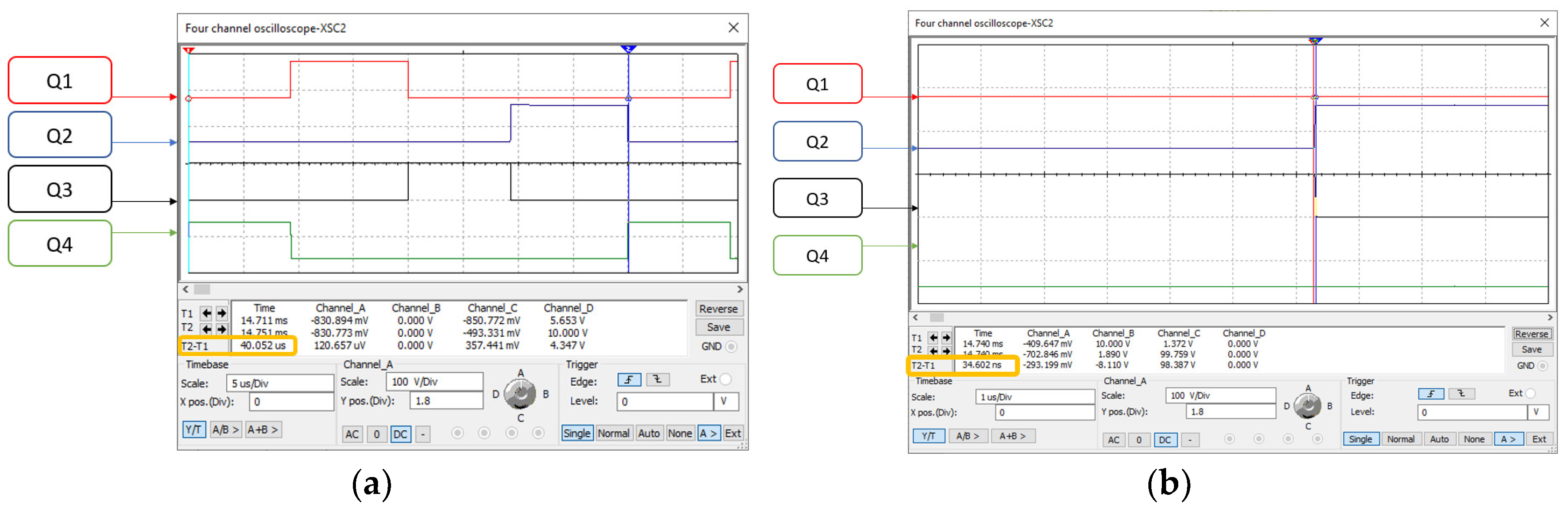
(a) Control sequence of synchronous interleaved configuration, total period is highlighted at 40 us, resulting in 25 kHz. (b) Dead time between MOSFET logic operation, maximum dead time is highlighted at 34.6 ns.
Figure 9.
(a) Control sequence of synchronous interleaved configuration, total period is highlighted at 40 us, resulting in 25 kHz. (b) Dead time between MOSFET logic operation, maximum dead time is highlighted at 34.6 ns.
All time sequences used in the simulation are described on the table below:
Table 4.
Timing required during the MISBC simulation for Buck Converter, Synchronized Buck Converter and Parallel Operation topologies.
Table 4.
Timing required during the MISBC simulation for Buck Converter, Synchronized Buck Converter and Parallel Operation topologies.
| (%) | ts | ||
|---|---|---|---|
| 80.0 | 20 µs | 3.95 µs | 16 µs |
| 60.0 | 20 µs | 7.95 µs | 12 µs |
| 48.0 | 20 µs | 10.35 µs | 9.6 µs |
| 40.0 | 20 µs | 11.95 µs | 8 µs |
| 34.3 | 20 µs | 13.09 µs | 6.86 µs |
| 30.0 | 20 µs | 13.95 µs | 6 µs |
| 26.7 | 20 µs | 14.62 µs | 5.33 µs |
| 24.7 | 20 µs | 15 µs | 4.95 µs |
Table 5.
Timing required during the MISBC simulation for Synchronous Interleaved Buck Converter.
| (%) | ts | ||
|---|---|---|---|
| 80.0 | Not Operational | Not Operational | Not Operational |
| 60.0 | Not Operational | Not Operational | Not Operational |
| 48.0 | 40 µs | 19.2 µs | 19.25 µs |
| 40.0 | 40 µs | 16 µs | 16.05 µs |
| 34.3 | 40 µs | 13.71 µs | 13.76 µs |
| 30.0 | 40 µs | 12 µs | 12.05 µs |
| 26.7 | 40 µs | 10.66 µs | 10.71 µs |
| 24.7 | 40 µs | 9.89 µs | 9.94 µs |
To ensure an accurate comparison with the prototype, a variable load was utilized, simulating a programmable load under a constant current set up. The same was applied to the power supply, which was also required to represent a constant current operation, while the input voltage was altered, changing the circuit duty cycle. The resistive load was altered to ensure depending on the duty cycle, ensuring a constant input current of 3A. This approach was established to reduce variables around the dead time definition and optimization, since the source current and load current impact the delay propagation at the charge and discharge cycles of each topology applied on the MISBC circuit. Figure 10 depicts the input voltage range utilized on the simulation.
Simulation Results and Analysis
Each topology simulated on the MISBC circuit presented a characteristic curve. Unfortunately, Multisim does not consider thermal deviations on the circuit performance based on the power loss on each component. Therefore, having a distributed path of the current flow consequent of the topology utilized on the parallel operation of both half bridge circuits, does not provide any advantages on the simulation. This condition is not sustained in a practical application, since RDS (on) and RΘJA impact the overall efficiency of the circuit.
The highest efficiency recorded during the simulation of the MISBC circuit was 98.54%, when the synchronous interleaved topology operated at was configured with 48% duty cycle. On the other hand, the lowest efficiency recorded was 92.8% with the parallel operation configured with 24.7% duty cycle. Figure 11 presents the simulated efficiency of different converters.
Based on the simulation, the disadvantage of having an interleaved topology for input voltages smaller than 48 Volts is clear, since the circuit output is almost continuous across both High Side MOSFET. To ensure the perfect operation of an interleaved topology, the conditions below must be maintained:
The results between the typical buck converter and synchronous buck converter topologies were similar. Although, the difference between each topology is proportional to the load demand.
Another factor which is relevant to mention is the output voltage ripple achieved during the MISBC circuit simulation, shown on Figure 12. The parallel operation reached a ripple of 0.576 V, which represents 2.45% of the output voltage achieved of 23.5 V when a duty cycle of 24.7% is applied to the input voltage of 97 V. This is a positive result, summarizing the worst performance of the MISBC across all topologies applied during the simulation. Figure 12 shows the simulated voltage ripple as a function of the duty cycle of the MOSFET.
Figure 12.
Output voltage ripple achieved during the MISBC simulation.
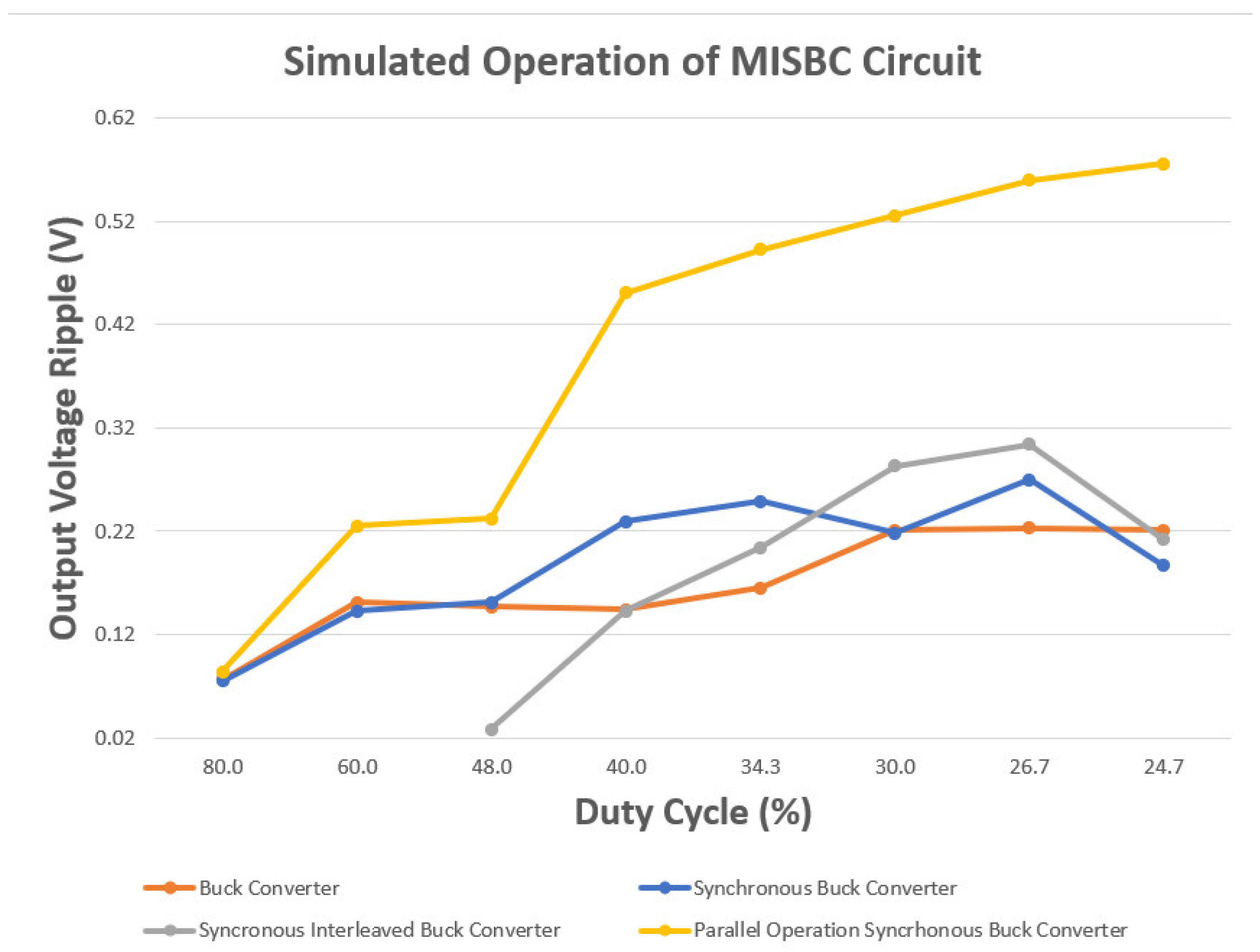
No duty cycle corrections were made to calibrate the output voltage achieved from the MISBC circuit to the desired output voltage of 24 V. Figure 12 shows the output voltage achieved from each topology. Despite having the largest voltage ripple, the parallel operation has achieved the highest output voltage. In contrast, the buck converter has a minimum output voltage of 23 V, resulting in an error of 4.16%.
Figure 12.
Output voltage range achieved during the MISBC simulation.
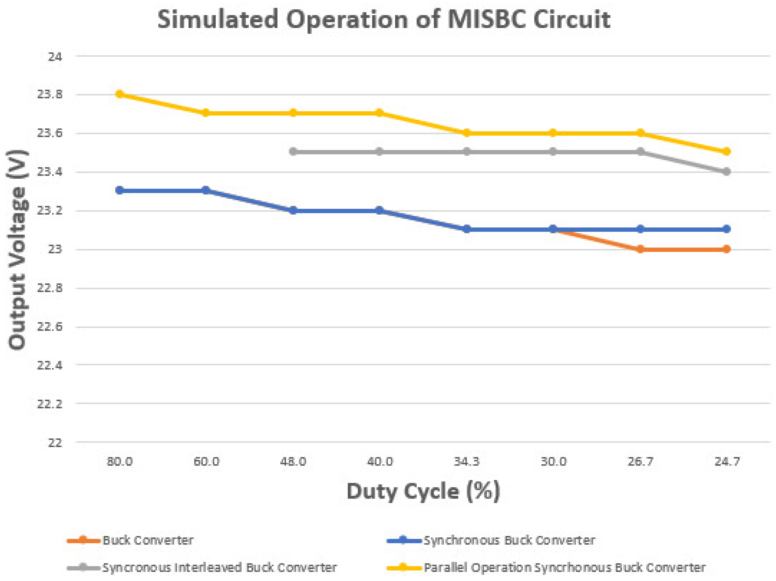
All results acquired during the simulation are an ideal guideline to evaluate the control algorithm used to operate the MISBC. However, the satisfactory outcome from the simulations clearly shows that all considerations taken towards line capacitance and inductance are valid.
6. Prototype Design and Evaluation
The PCBA design and layout of the MISBC circuit is a critical step towards the system evaluation. Critical features such as track capacitance and inductance must be considered to minimize the effects of parasitic inductance and capacitance and propagation delay mismatch of the control signals, which directly affect the dead time required between each MOSFET activation. The implementation of anti-parallel circuits and multilayer PCBA with ground shielded plane address potential issues towards line inductance and parasitic capacitance.
The PCB layout, structure and track work were developed based on IPC-2221C:2023 [20] “Generic Standard on Printed Board Design”, with emphasis on thermal management, capacitance, and inductance considerations, ensuring the optimal construction and design of the MISBC circuit prototype.
A multilayer structure, consisting of four layers, was utilized on the MISBC prototype. The top layer has a thickness of 2 oz of copper, to ensure the integrity of creepage distances between each component during the manufacturing process. All other layers were constructed with 4 oz of copper, to increase the thermal dissipation and reduce the inductance at the control line.
Additional considerations for snub circuits across the power switching circuit and calibration of bootstrap circuits ensure that overshooting and resonance propagation were addressed during development and circuit evaluation.
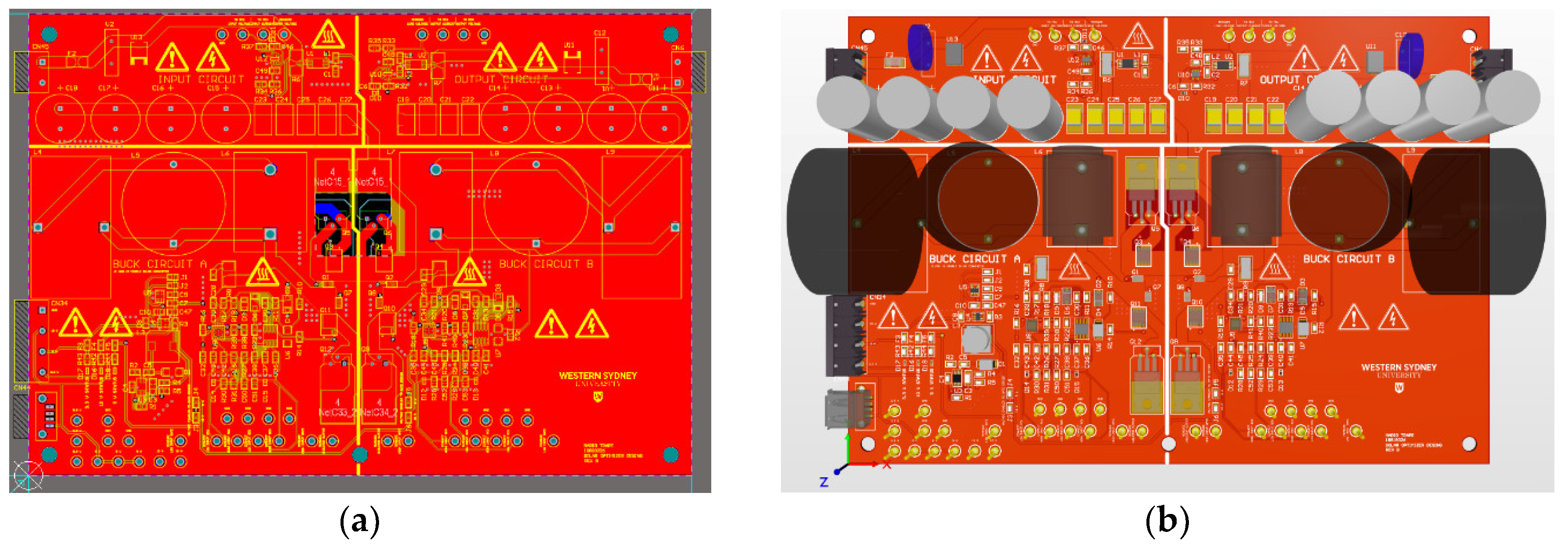
Figure 13.
(a) 2D view of the P.C.B. design in Altium Designer; (b) 3D view of the P.C.B. design in Altium Designer.
Figure 13.
(a) 2D view of the P.C.B. design in Altium Designer; (b) 3D view of the P.C.B. design in Altium Designer.
During the PCB design, clearance and creepage distances were implemented, based on the IEC 61010-1:2010 [21] “Safety requirements for electrical equipment for measurement, control, and laboratory use- Part 1: General requirements”. The MISBC circuit must be classified as a secondary circuit, without a direct connection to the grid or power source with a nominal voltage greater than 300 Vrms, since the maximum clearance and creepage achieved between polarities was 0.25 mm, in a circuit with nominal operation of 100 V.
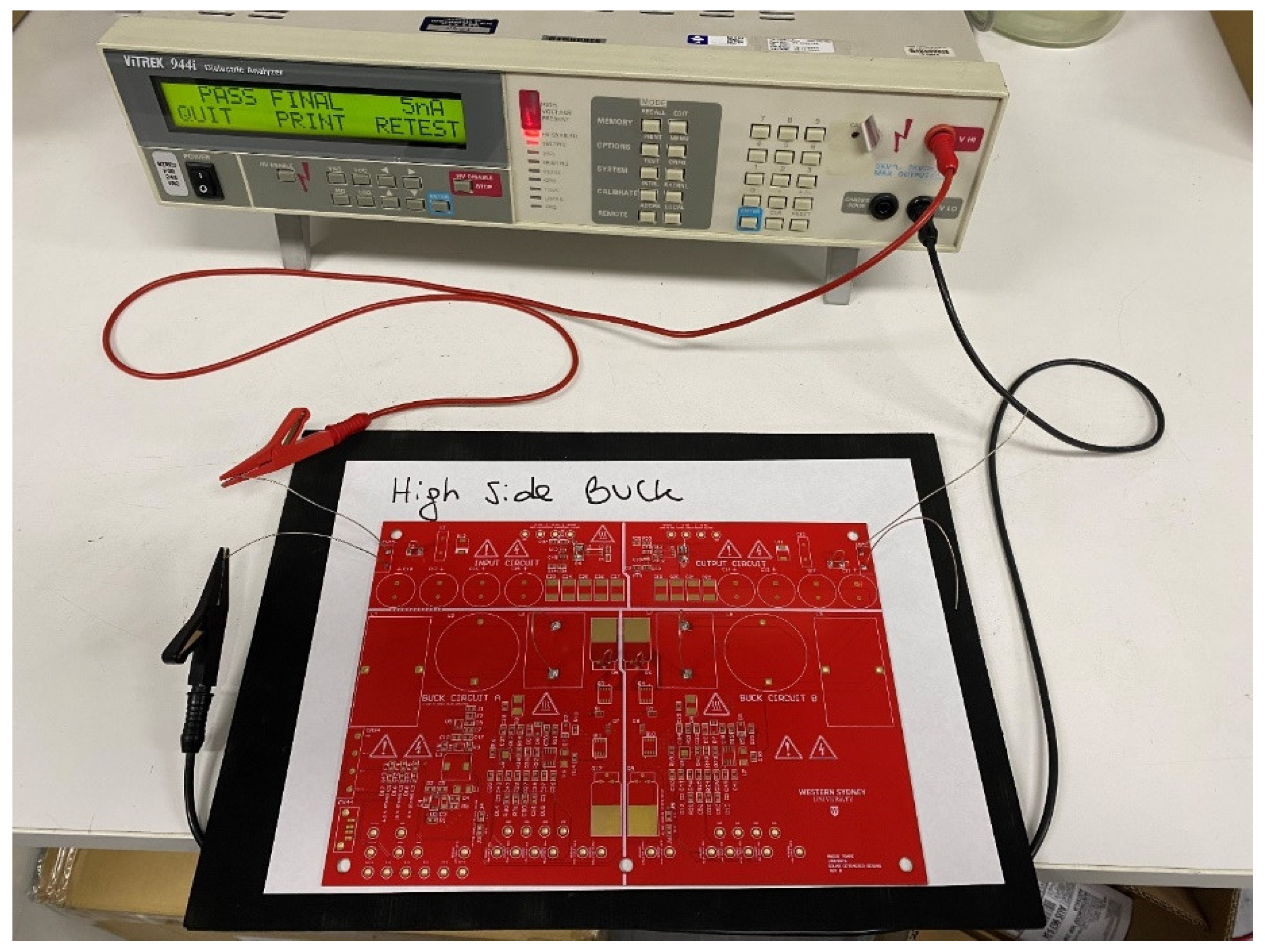
To ensure that the clearance and creepage distances selected for the MISBC circuit were adequate, a dielectric strength test was performed across each MOSFET footprint. The dielectric tester utilized for the PCB design evaluation was a Vitrek 944i- Dielectric Analyzer. Figure 12 shows how the test was set up.
The dielectric test was configured with a ramp up setting, where the generated voltage from the dielectric tested increases by 100 VDC per second. The maximum leakage current configured for the alarm at the dielectric tester was 10 µA. The maximum voltage achieved during the test was 1000 VDC, and the maximum leakage current achieved across the MOSFET footprint was lower than 1 µA. Based on this result, the circuit was successfully validated.
Figure 14.
Dielectric test set up.
To evaluate the prototype built as a platform-based with MISBC circuit, a bench test set up was configured with a programmable power supply, programmable load, multimeters, oscilloscopes, and signal generators. To ensure that all gate signals can be acquired on the half bridge circuit, a set of differential probes was coupled to one of the oscilloscope units. Positive Temperature Coefficient (PTC) sensors were also installed into the prototype, ensuring that a thermal evaluation of the circuit was also performed. In summary, the proposed test set up depicted in Figure 15, clearly shows the location and layout used on the test bench.
The table below describes all equipment used during the evaluation tests of the prototype.
Table 6.
Equipment utilized during the prototype evaluation.
| Description | Manufacturer | Quantity | |
|---|---|---|---|
| XTR 300-2.8 | Power supply | Xantrex, California, USA. | 1 |
| DT4252 | Multimeter | Hioki, Nagano, Japan | 2 |
| U1242B | Multimeter | Keysight, California, USA. | 4 |
| DSOX2024A | Oscilloscope | Keysight, California, USA. | 1 |
| RTB2004 | Oscilloscope | Rohde & Schwarz, Munich, Germany | 2 |
| 33500B | Signal Generator | Keysight, California, USA. | 4 |
| 72-13210 | Programmable Load | Tenma, Ohio, USA. | 1 |
| DM330028 | Development Board | Microchip Technology, Arizona, USA. | 1 |
Figure 16 depicts all connections made into the platform-based prototype and segregates each operational block used during the hardware evaluation, also represented in Figure 2.
The control circuit was triggered and supervised by the dsPIC controller, existing on the DM330028 development board. The controller was responsible for acquiring voltage and current measurements from the input and output circuit, as well as set the trigger point for each signal generator. This approach was employed to mitigate the effects of PWM jitter, which causes frequency oscillations in the control circuit due to delay functions in the microcontroller’s firmware. Although the DM330028 development board features a dsPIC33 chip with a 16-bit resolution PWM module and dedicated registers for phase shifting between each PWM output, the focus of this paper is on evaluating the hardware and switching characteristics of the MISBC circuit, rather than the implemented algorithm. Therefore, the dsPIC33 chip was utilized as a supervisory device, evaluating the shunt and condition monitoring circuit implemented in the prototype.
The utilization of dPIC33 chip as a supervisory device also allows the automatic shutdown of the control depending on the input and output power characteristics of the MISBC circuit. Figure 17 illustrates the control diagram utilized with the dsPIC33 during the MISBC circuit evaluation.
Considerations for Performance Evaluation
As a complementary approach to the hardware evaluation, an overshoot analysis of the control signal generated across the system was performed, to ensure that all considerations taken during research and development of the PCB are evaluated. All control signals generated by the signal generated were analyzed through the oscilloscope, under open voltage condition, and load condition, where the signal generator drives each gate driver.
This analysis ensures that any additional noise generated from the signal generators is subtracted during the hard and soft switching evaluation, which defines the effects of parasitic capacitance and inductance across the control line, which may generate additional overshooting of the switching signal. Figure 18 clearly shows an example of the process taken into consideration for the performance evaluation of the MISBC circuit operation as a synchronous buck converter, where an 80% duty cycle was required to convert 30 V to 24 V.
This configuration, operating at 80% duty cycle, received a signal with 13.9% overshoot at the High Side, which resulted in an overshoot of 19% at the MOSFET. Therefore, the PCBA design has an impact of 5.1% overshoot on the High Side. This is a good reference to have as a base, for further analysis of the results. Additionally, it is common to have an overshoot higher at the High Side switching, as it uses a virtual ground reference between the half bridge configuration, while the Low Side switching circuit uses circuit ground as a reference, since the circuit is not isolated, there is minimum oscillation at the circuit.
The worst overshoot value identified on the circuit was during the operation of the interleaved synchronous buck converter, depicted in Figure 19.
During the analysis of the overshoot voltage highlighted in Figure 19, the same overshoot value identified at the signal generators outputs and depicted in Figure 18 were identified. Therefore, during the operation of the interleaved synchronous topology, the High Side overshoot value reached 12.39% at 26.38% duty cycle, and 23.25% overshoot at 47.74% duty cycle.
Another factor to consider is that during the control circuit evaluation, a negligible mismatched delay propagation of each MOSFET was identified. Therefore, an accurate dead time was achieved with the PCBA design and layout.
Test Results and Analysis
All tests performed with the MISBC prototype were conducted within an environment with climate control, ensuring that a temperature of 24°C is maintained during the prototype evaluation. Figure 20 shows the results acquired from the prototype evaluation. The same voltage variation shown in Figure 10 was applied to the system. The highest efficiency achieved was 95.33%, during the parallel operation of the MISBC circuit at 60% duty cycle, which is completely opposite to the simulated results. The synchronous buck circuit presented the lowest efficiency compared to all other topologies with 88.14% at 24.7% duty cycle.
The same time reference used in the simulation was also used in the prototype evaluation. Although, the lowest dead time recorded was 2.4 µs. This dead time does not impact the logic transition time required by the gate driver, or the circuit switching capabilities.
Figure 21 depicts the output voltage ripple achieved during the MISBC prototype evaluation; the buck converter topology reached a voltage ripple of 0.82 V while the circuit had an output voltage of 21.6 V. Therefore, it had a ripple of 3.7% when a duty cycle of 34.29% was applied. This was the highest ripple recorded during the simulation and prototype evaluation of the MISBC circuit. Typically, the industry acceptance towards voltage ripple is 5%. Therefore, achieving a result of 3.7% is satisfactory.
During the prototype evaluation, no calibration of the duty cycle was performed to match the performance acquired during the simulation. The output voltage range recorded during the prototype evaluation is depicted in Figure 22. The lowest voltage output recorded was 21.16 V, while the highest voltage recorded was 22.64 V.
The biggest distinction between the simulation and the prototype evaluation is the temperature rise of each component. To illustrate the impact of the temperature, rise at the MOSFET, Figure 23 shows the temperature rise coefficient acquired at the High Side MOSFET Q1, which is activated during all operational topologies implemented on the MISBC circuit.
The temperature rise coefficient was sensed with two PTC sensors connected to two distinct multimeters (U1242B). Both sensors were connected to the same MOSFET, and the average value between both measurements acquired from each multimeter, was then subtracted from the ambient temperature recorded from the same multimeter. Consequently, the value registered was the temperature rise of the MOSFET above ambient temperatures.
The temperature rise of the MOSFET is a result of the power dissipated at the junction temperature, which is a combination of switching losses ( and conductivity losses (. With the increase of the junction temperature (), the resistance between drain and source (RDS (on)) also increases, therefore generating more conductivity losses.
Maintaining a stable circuit is part of the circuit evaluation. Based on that, having a maximum temperature rise at the MOSFET of 64°C is acceptable, but not ideal. Since the device temperature will be close to 90°C when the ambient temperature is 24°C, this rating limits applications of the MISBC circuit using the IRF530N with a synchronous buck converter topology.
Figure 24 depicts the overall efficient results from the prototype evaluation with an additional trendline based on second order polynomial equation. This approach is required to convert the efficiency curve into a mathematical equation, allowing it to be incorporated into any control algorithm.
The following second order polynomial equations, correlates the output efficiency from Figure 24 against the duty cycle applied on the MISBC circuit during prototype evaluation.
Each equation provided can be used in a closed loop comparison firmware, ensuring the instant output power performance acquired from the circuit matches with the characterization curve of the MISBC prototype, enabling soft corrections on the duty cycle and identifying potential issues with the circuit during abnormal conditions.
To evaluate the hardware utilized, a direct comparison of the MISBC circuit was performed against a Mean Well DC-DC converter, which is widely implemented on railway, industrial control, factory automation, and telecommunications and data communication systems. It is important to disclose, that the Mean Well is a product that complies with Radiated Electromagnetic Interference (EMIrad) and Conducted Electromagnetic Interference (EMIcon) standards and provides a high voltage isolation across each input and output connection. These requirements tend to impact the overall efficiency of the circuit. The MISBC circuit discussed in this paper does not comply with these standards.
The topology implemented on the Mean Well DC-DC converter is not publicly available. Therefore, all topologies disclosed in this paper will be compared with the Mean Well product series. The table below shows the data collected from the Mean Well DDR-240 Series datasheet [22], compared with the MISBC circuit. The reference point used for the Mean Well DC-DC converter was at 100% load demand, resulting in a 240W, while the MISBC results were acquired at 260W.
The following nomenclature was used to compare the topologies available on the MISBC circuit with the DDR-240 Series DC-DC converter.
- Topology 1 = Buck Converter
- Topology 2 = Synchronous Buck Converter
- Topology 3 = Synchronous Interleaved Buck Converter
- Topology 4 = Parallel Operation Synchronous Buck Converter
Based on the results shown in Table 7, the DDR-240C-24 converter matches the performance of the buck converter, but it has a lower performance than any other topology applied on the MISBC circuit. However, the DDR-240D-24, has a better efficiency when compared to the buck and synchronous buck converters. This comparison shows how the Synchronous Interleaved Buck Converter, and the Parallel operation of Synchronous Buck Converter is a powerful and resourceful topology providing results above 92.5%.
7. Conclusions and Future Work
In the future, additional MOSFETs will be evaluated on the MISBC prototype, such as Si based MOSFET (FDS10C4D2N) and GaN based MOSFET (GAN 3R2-100 CBE), which presents much better ratings in comparison with the IRF530N. Consequently, an additional gate driver (LM5113-Q1), will also be required to interface the GaN MOSFET to the control circuit. Once additional MOSFETs are added to the MISBC circuit, the overall performance can be evaluated for a higher frequency range, reaching up to 1 MHz. Circuit life span will also be analyzed using accelerated deterioration techniques to evaluate each MOSFET based in their RDS (on) values, and oscillations over different topologies and operating conditions.
Radiated Electromagnetic Interference (EMIrad) and Conducted Electromagnetic Interference (EMIcon) tests will be performed to analyze the performance of the MISBC prototype.
This paper’s overall outcome is to identify potential transitioning points between each topology, while highlighting the differences in efficiency, output voltage, output voltage ripple and temperature rise, while highlighting the limitations associated with the IRF530N due to its electrical characteristics.
The objective of this paper was to evaluate the design of a platform based MISBC circuit, through a prototype, including component selection, simulation, PCB construction and output performance of each topology allowed by the MISBC with Si MOSFETs. These results allow the definition of performance trendline, which is required for algorithm development maximizing the efficiency output of the circuit, while using all topologies.
A brief comparison between the MISBC circuit with the DDR-240 converter series designed and manufactured by Mean Well, allowed a benchmark comparison with components successfully implemented into the market.
With the evaluation of the MISBC prototype, an algorithm can also be implemented into the dsPIC board, enabling the transition between circuit topologies depending on the load characteristics and voltage input range under steady state transitions and load fluctuation analysis. The key findings from the design and performance analysis of the platform based MISBC circuit are:
- Interleaved Synchronous Buck Converter boosts the overall efficiency of the circuit. However, it implies limiting operating conditions, compared with any other topology in a MISBC circuit.
- Simulations in Multisim do not account for thermal characteristics. Therefore, simulating the Parallel Operation Synchronous Buck Converter does not provide an accurate result.
- Additional thermal optimizations on the PCBA are required to stabilize the IRF530N when operating under Synchronous Buck and Buck topologies.
- The MISBC topology can reach up to 95.33% efficiency depending on the load demand and duty cycle required from the switching circuit when the IRF530N is utilized.
In summary, the MISBC circuit is an efficient and resourceful approach towards buck converters, providing a redundant and powerful solution for wide input voltage DC-DC converters, which can be deployed into several applications, being portable or stationary, as long as the input and output voltage requirements meet the system design characteristics.
Author Contributions
Conceptualization, MAT; methodology, MAT; validation, MAT; supervision AH, JR, and MN; writing—original draft preparation, MAT All authors have read and agreed to the published version of the manuscript.
Funding
This work was funded by the School of Engineering, Design and Built Environment, Western Sydney University (project code 20870.74954).
Institutional Review Board Statement
Not applicable.
Informed Consent Statement
Not applicable.
Data Availability Statement
All relevant data are included in this paper.
Conflicts of Interest
Not applicable.
References
- T.-D. Tran, H. Cha, V.-D. Bui, and C. V. Nguyen, “Derivation of Small-Signal Model of Boost-SEPIC Interleaved Converter Based on PWM Switch Model,” in 2023 International Symposium on Electrical and Electronics Engineering, ISEE 2023, October 19, 2023 - October 20, 2023, Ho Chi Minh City, Vietnam, 2023: Institute of Electrical and Electronics Engineers Inc., in Proceedings - 2023 International Symposium on Electrical and Electronics Engineering, ISEE 2023, pp. 185-190. [CrossRef]
- N. Abdelhadi, B. M. Ridha, M. Rabia, B. Abdelkader, A. B. Tekkouk, and B. Zineb, “Integrated Interleaved Transformer in an Isolated Full-Bridge Buck Converter∗,” 2024. [CrossRef]
- W. C. Leal, M. O. Godinho, R. F. Bastos, C. R. De Aguiar, G. H. F. Fuzato, and R. Q. MacHado, “Cascaded Interleaved DC-DC Converter for a Bidirectional Electric Vehicle Charging Station,” IEEE Transactions on Industrial Electronics, vol. 71, no. 4, pp. 3708-3717, 2024. [CrossRef]
- M. Yousuf and K. Zeb, “Design and Analysis of DC-DC Two-Phase Interleaved Buck Converter for EV Charging Applications,” in 2023 18th International Conference on Emerging Technologies (ICET), 6-7 Nov. 2023, 2023, pp. 80-85. [CrossRef]
- S. Benzaouia, N. Msirdi, A. Rabhi, B. K. Oubbati, and S. Zouggar, “Interleaved Boost Converter Control Technique Improvements for Fuel Cell Electric Vehicles,” in 3rd International Conference on Electronic Engineering and Renewable Energy, ICEERE 2022, May 20, 2022 - May 22, 2022, Saidia, Morocco, 2023, vol. 954: Springer Science and Business Media Deutschland GmbH, in Lecture Notes in Electrical Engineering, pp. 599-609. [CrossRef]
- L. Pirashanthiyah, H. N. Edirisinghe, W. M. P. De Silva, S. R. A. Bolonne, V. Logeeshan, and C. Wanigasekara, “Design and Analysis of a Three-Phase Interleaved DC-DC Boost Converter with an Energy Storage System for a PV System,” Energies, vol. 17, no. 1, 2024. [CrossRef]
- R. Subbulakshmy and R. Palanisamy, “SVPWM control strategy for Novel Interleaved High Gain DC converter fed 3-level NPC Inverter for Renewable Energy Applications,” ISA Transactions, vol. 140, pp. 426-437, 2023/09/01/ 2023. [CrossRef]
- Y. Gaaloul, O. B. H. B. Kechiche, and M. Hamouda, “Modeling and Simulation of a Two-Phase Interleaved Boost Converter for Photovoltaic Applications,” in 2023 IEEE International Conference on Artificial Intelligence and Green Energy, ICAIGE 2023, October 12, 2023 - October 14, 2023, Sousse, Tunisia, 2023: Institute of Electrical and Electronics Engineers Inc., in 2023 IEEE International Conference on Artificial Intelligence and Green Energy, ICAIGE 2023. [CrossRef]
- K. A. Singh, A. Prajapati, and K. Chaudhary, “High-Gain Compact Interleaved Boost Converter with Reduced Voltage Stress for PV Application,” IEEE Journal of Emerging and Selected Topics in Power Electronics, vol. 10, no. 4, pp. 4763-4770, 2022. [CrossRef]
- X.-F. Cheng, Q. Zhao, D. Wang, C. Liu, and Y. Zhang, “A high step-up multi-phase interleaved boost converter for fuel cells power system,” International Journal of Hydrogen Energy, vol. 56, pp. 667-675, 2024/02/22/ 2024. [CrossRef]
- X. Guo et al., “A new multi-mode fault-tolerant operation control strategy of multi-phase stacked interleaved Buck converter for green hydrogen production,” International Journal of Hydrogen Energy, vol. 47, no. 71, pp. 30359-30370, 2022/08/19/ 2022. [CrossRef]
- X. Hao, I. Salhi, S. Laghrouche, Y. Ait-Amirat, and A. Djerdir, “Robust control of four-phase interleaved boost converter by considering the performance of PEM fuel cell current,” International Journal of Hydrogen Energy, vol. 46, no. 78, pp. 38827-38840. [CrossRef]
- Rana, N.; Sonar, S.; Banerjee, S. Performance Investigation of Closed-Loop Dual Phase Interleaved Buck-Boost Converter with Dragonfly Optimized Type-III Controller. IEEE Trans. Circuits Syst. II Express Briefs 2022, 69, 1472–1476. [CrossRef]
- Zakaria, A.; Marei, MI; Mashaly, H.M. A Hybrid Interleaved DC-DC Converter Based on Buck-Boost Topologies for Medium Voltage Applications. e-Prime—Adv. Electr. Eng. Electron. Energy 2023, 6, 100301. [CrossRef]
- P. Zhang, Y. Liu, J. Zhao, H. Zhang, and Q. Lv, “An Efficiency Optimization Control Method with Fast Dynamic Response for Muti-Phase Interleaved BUCK Converter,” in IECON 2021 – 47th Annual Conference of the IEEE Industrial Electronics Society, 13-16 Oct. 2021, 2021, pp. 1-5. [CrossRef]
- G. Banerjee, A. Dey, and M. Sengupta, “Analytical and experimental studies on improved performance high frequency multi-phase synchronous DC-DC converter using SiC MOSFETs and coupled inductors,” Sadhana - Academy Proceedings in Engineering Sciences, Article vol. 49, no. 1, 2024, Art no. 28. [CrossRef]
- P. Kaur, P. Jaswal, and A. Gupta, “Efficiency enhancement in a switched capacitor cell interleaved buck converter using GaN-FETs,” International Journal of Power Electronics and Drive Systems, Article vol. 15, no. 3, pp. 1547-1563, 2024.
- S. Liu, G. Dong, T. Mishima, and C. M. Lai, “Over 98% Efficiency SiC-MOSFET Based Four-Phase Interleaved Bidirectional DC-DC Converter Featuring Wide-Range Voltage Ratio,” IEEE Transactions on Power Electronics, Article vol. 39, no. 7, pp. 8436-8455, 2024. [CrossRef]
- Y. I. Mesalam, S. Awdallh, H. Gaied, and A. Flah, “Interleaved Bidirectional DC-DC Converter for Renewable Energy Application based on a Multiple Storage System,” Engineering, Technology and Applied Science Research, Article vol. 14, no. 2, pp. 13329-13334, 2024. [CrossRef]
- IPC International. Generic Standard on Printed Board Design; IPC-2221C; I.P.C. International: Bannockburn, IL, U.S.A., 2023.
- International Electrotechnical Commission (IEC). Safety Requirements for Electrical Equipment for Measurement, Control, and Laboratory Use—Part 1: General Requirements; IEC 61010-1:2010; IEC: Geneva, Switzerland, 2010.
- MEAN WELL. DDR-240 Series: DIN Rail Type DC-DC Converter. Available online: https://www.meanwell.com/Upload/PDF/DDR-240/DDR-240-spec.pdf (accessed on 16 September 2024).
Figure 1.
The methodology utilized to develop the MISBC prototype platform.
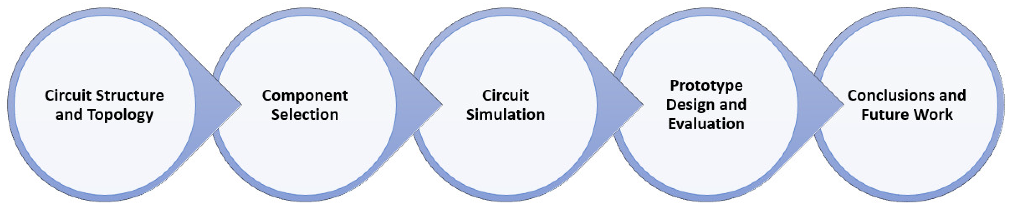
Figure 2.
Schematic Diagram utilized on the platform base MISBC circuit.
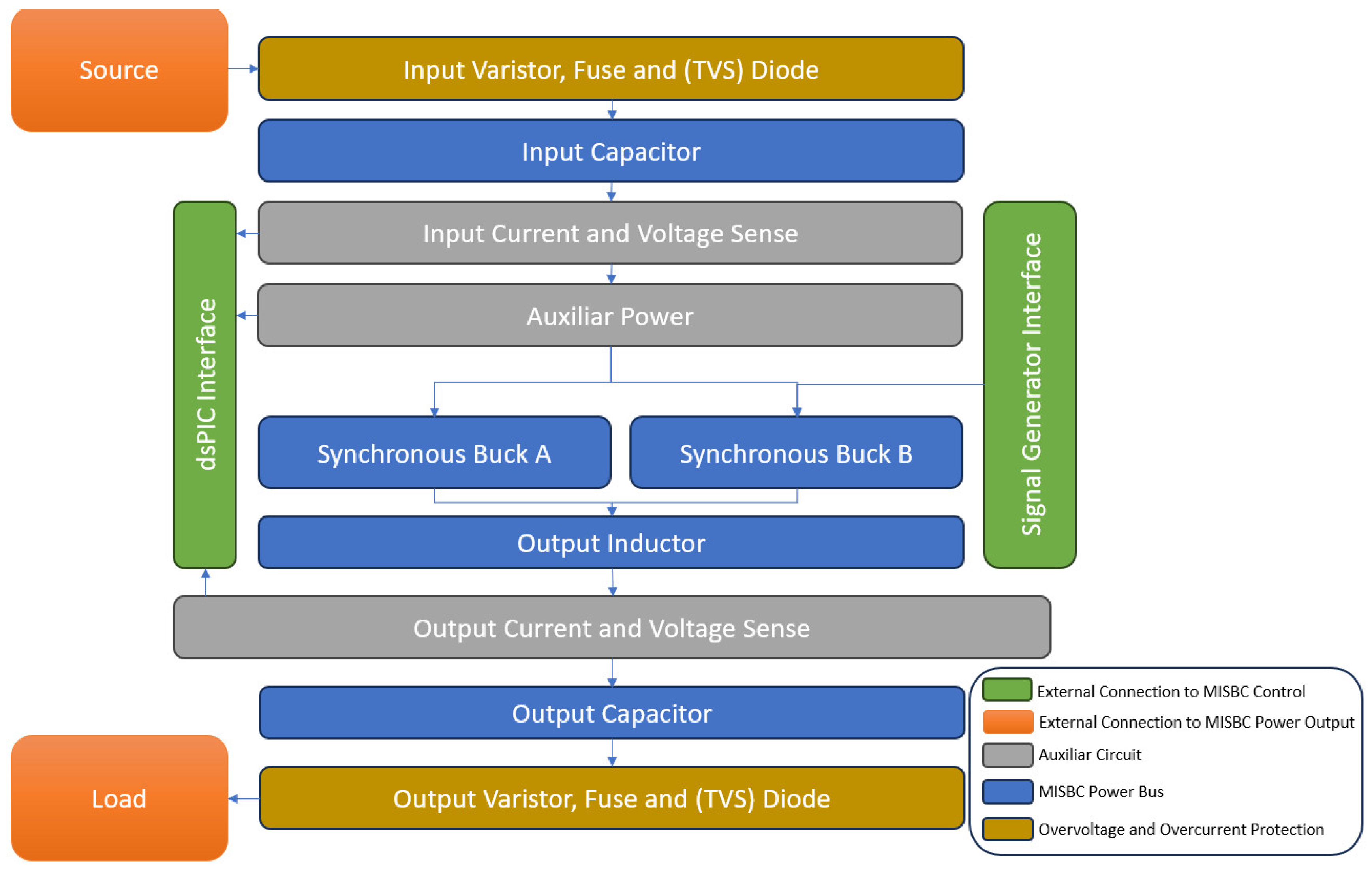
Figure 3.
Simplified Schematic of MISBC circuit operation.
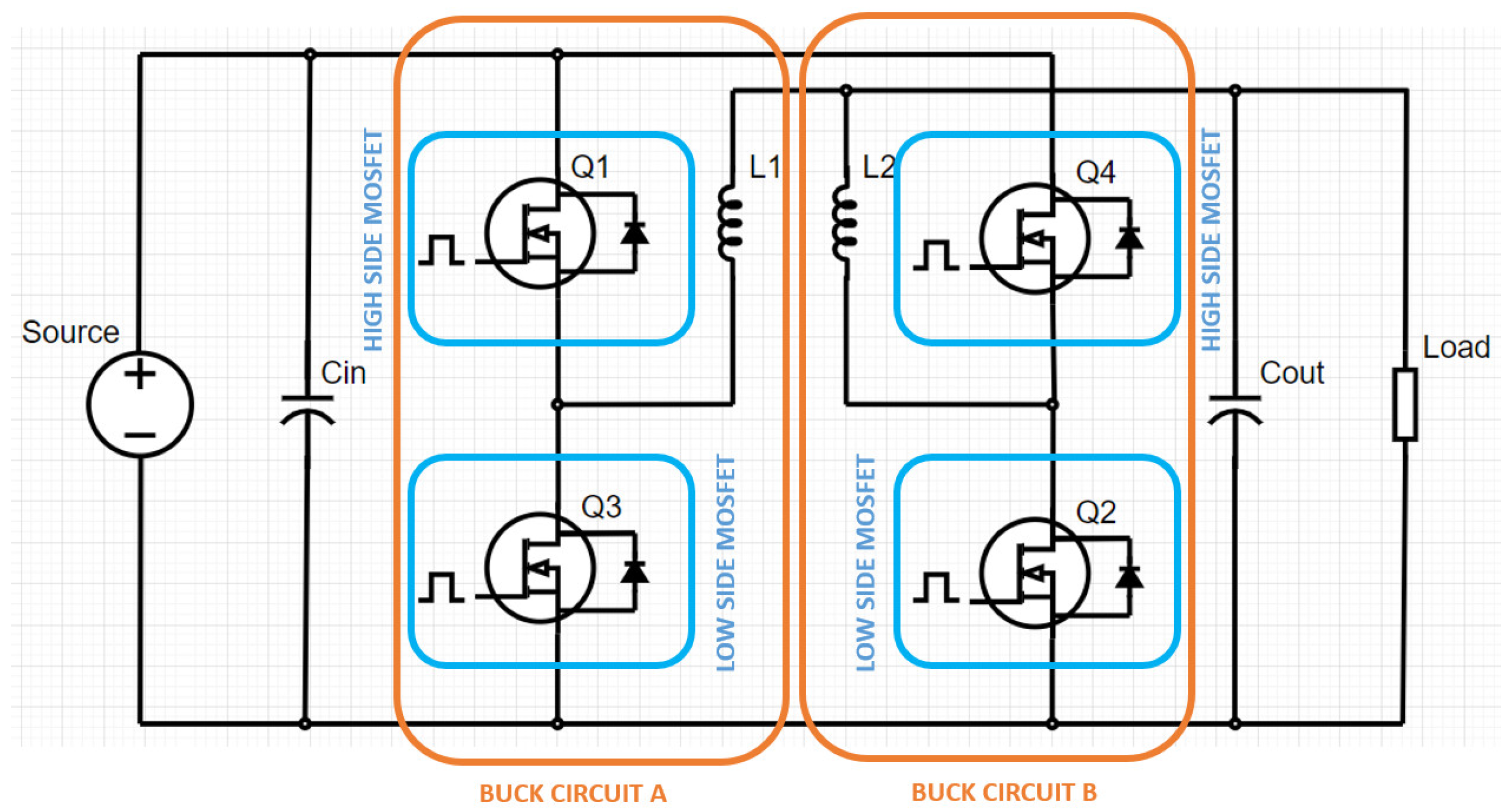
Figure 4.
(a) Charge cycle of a conventional buck operation; (b) Discharge cycle of a conventional buck operation; (c) Timing diagram required in a conventional buck operation.
Figure 4.
(a) Charge cycle of a conventional buck operation; (b) Discharge cycle of a conventional buck operation; (c) Timing diagram required in a conventional buck operation.
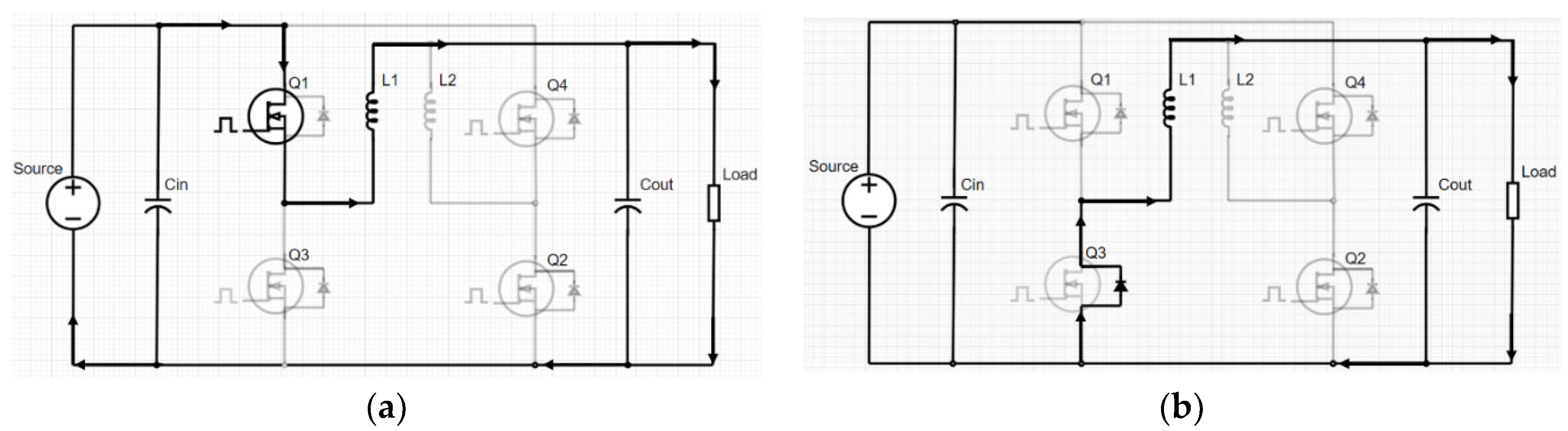
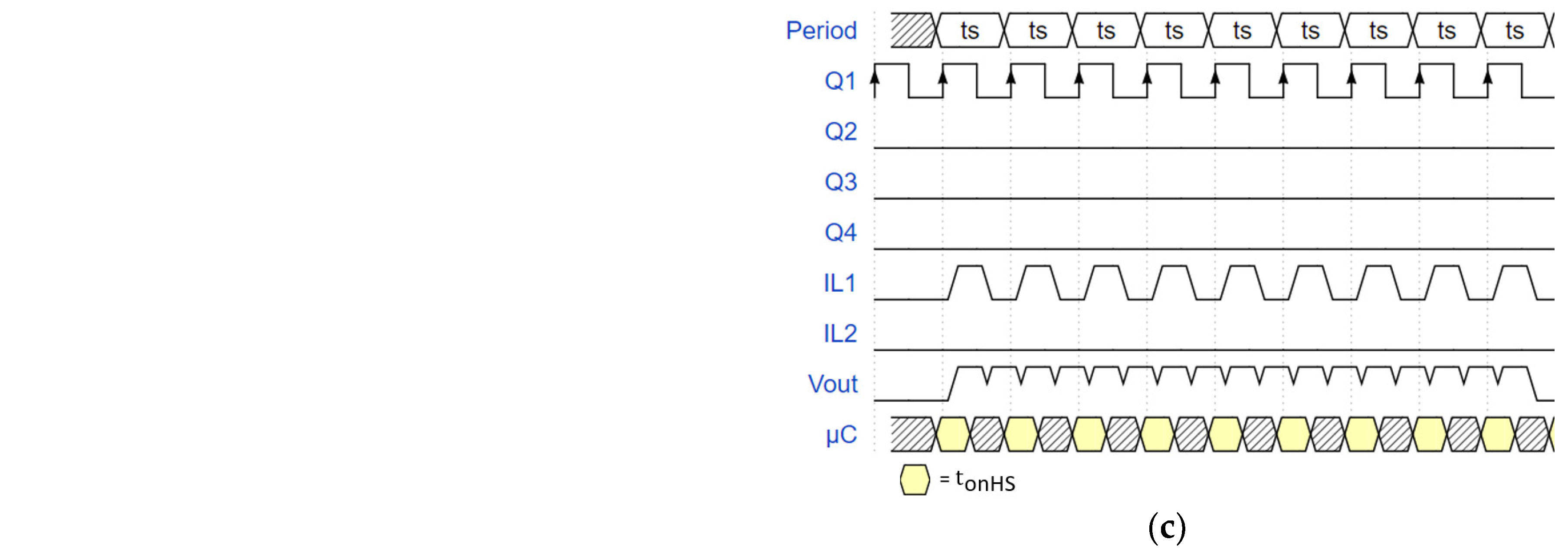
Figure 6.
(a) Charge cycle of an interleaved buck operation at Buck Circuit A; (b) Discharge cycle of an interleaved buck operation at Buck Circuit A (c) Charge cycle of an interleaved buck operation at Buck Circuit B; (d) Discharge cycle of an interleaved buck operation at Buck Circuit B; (e) Timing diagram required for a synchronous interleaved buck operation.
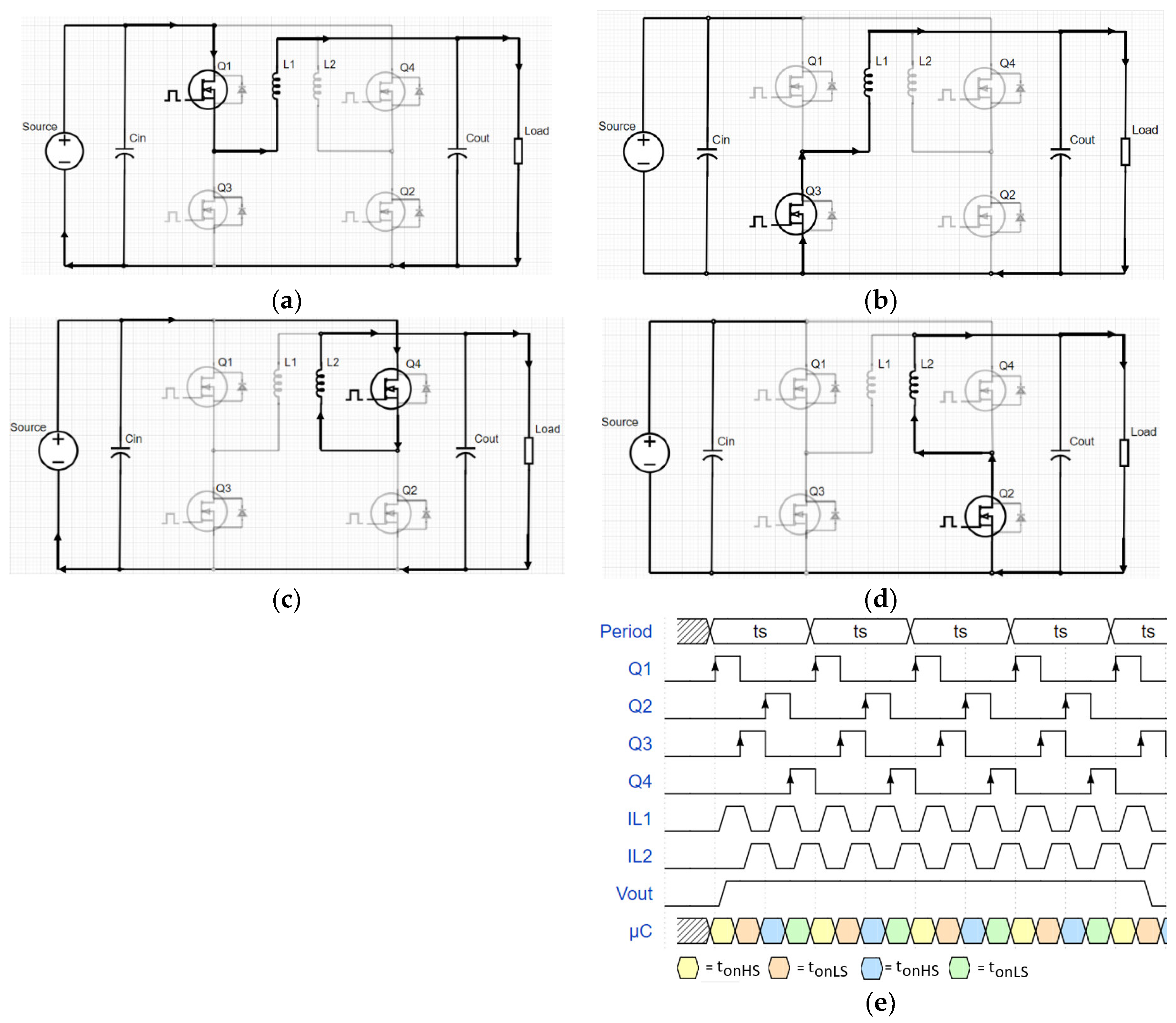
Figure 8.
A Simplified circuit diagram was utilized during the simulation of the MISBC circuit in Multisim.
Figure 8.
A Simplified circuit diagram was utilized during the simulation of the MISBC circuit in Multisim.
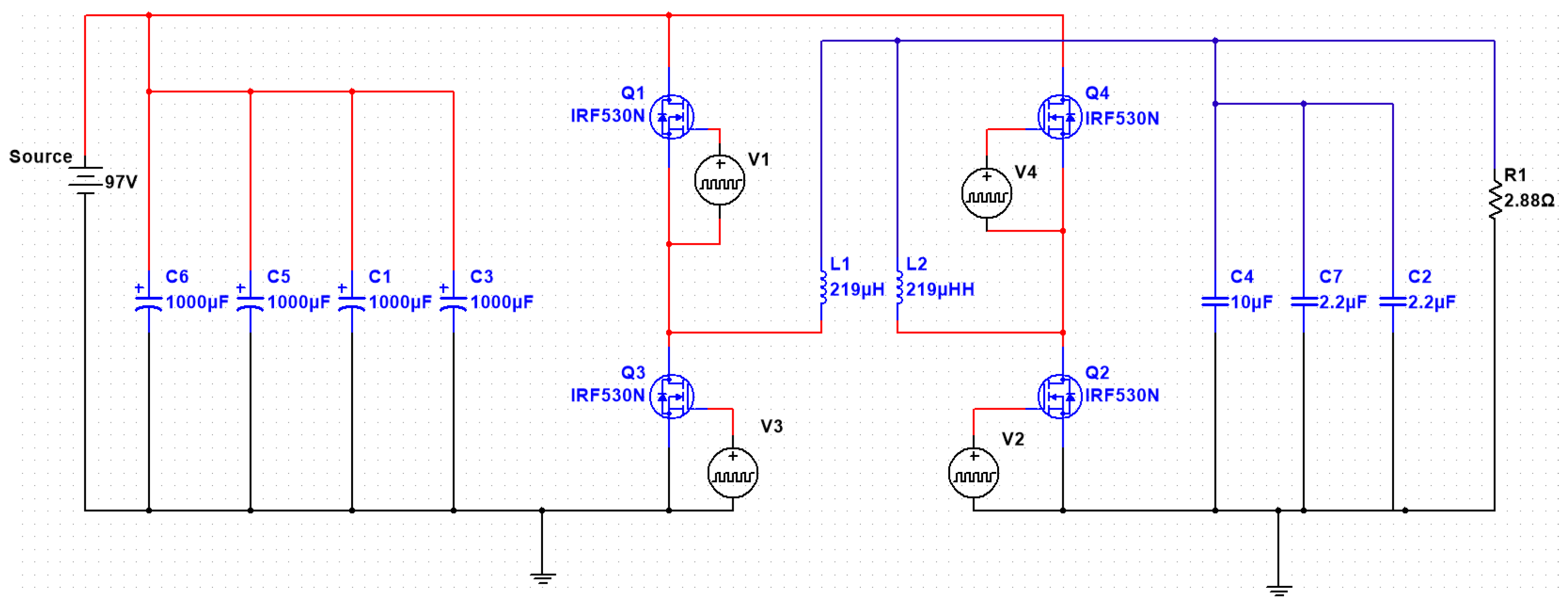
Figure 10.
Voltage input and duty cycle configuration used on the MISBC circuit simulation in Multisim.
Figure 10.
Voltage input and duty cycle configuration used on the MISBC circuit simulation in Multisim.
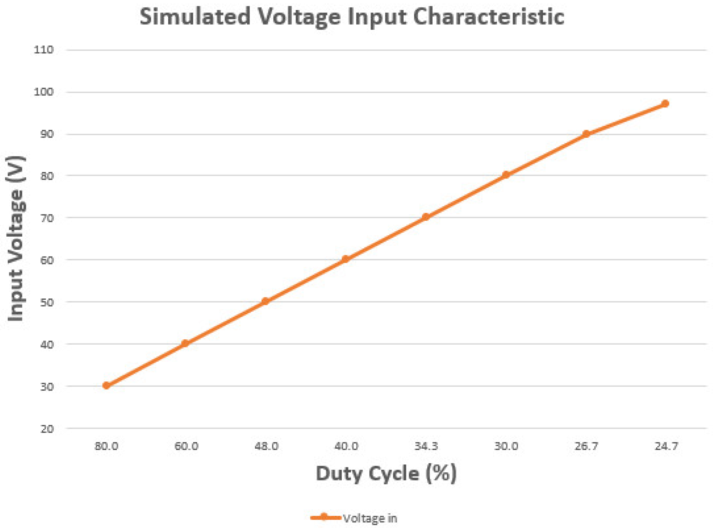
Figure 11.
Efficiency results from the MISBC Simulation.
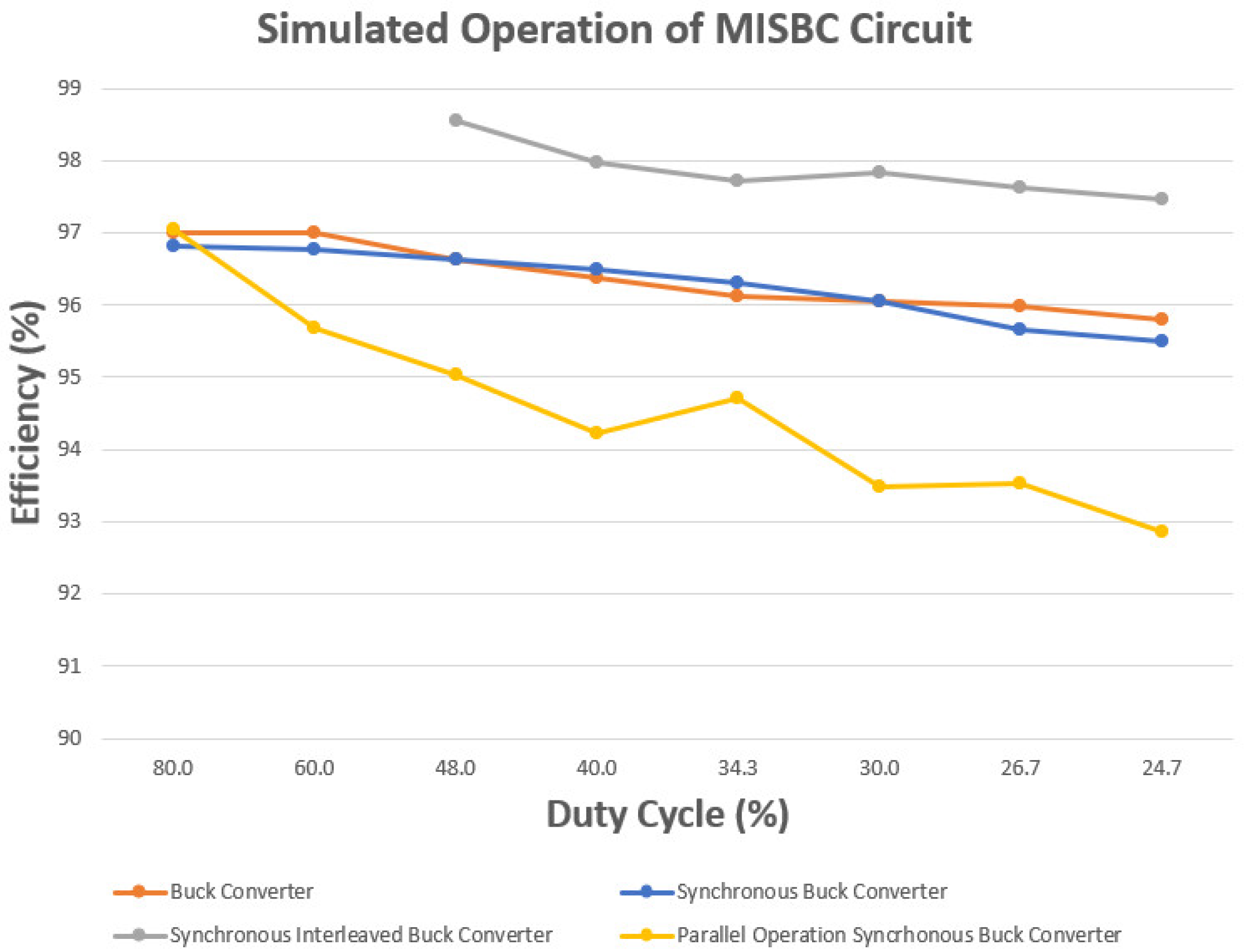
Figure 15.
Bench test set up, used to evaluate the prototype.
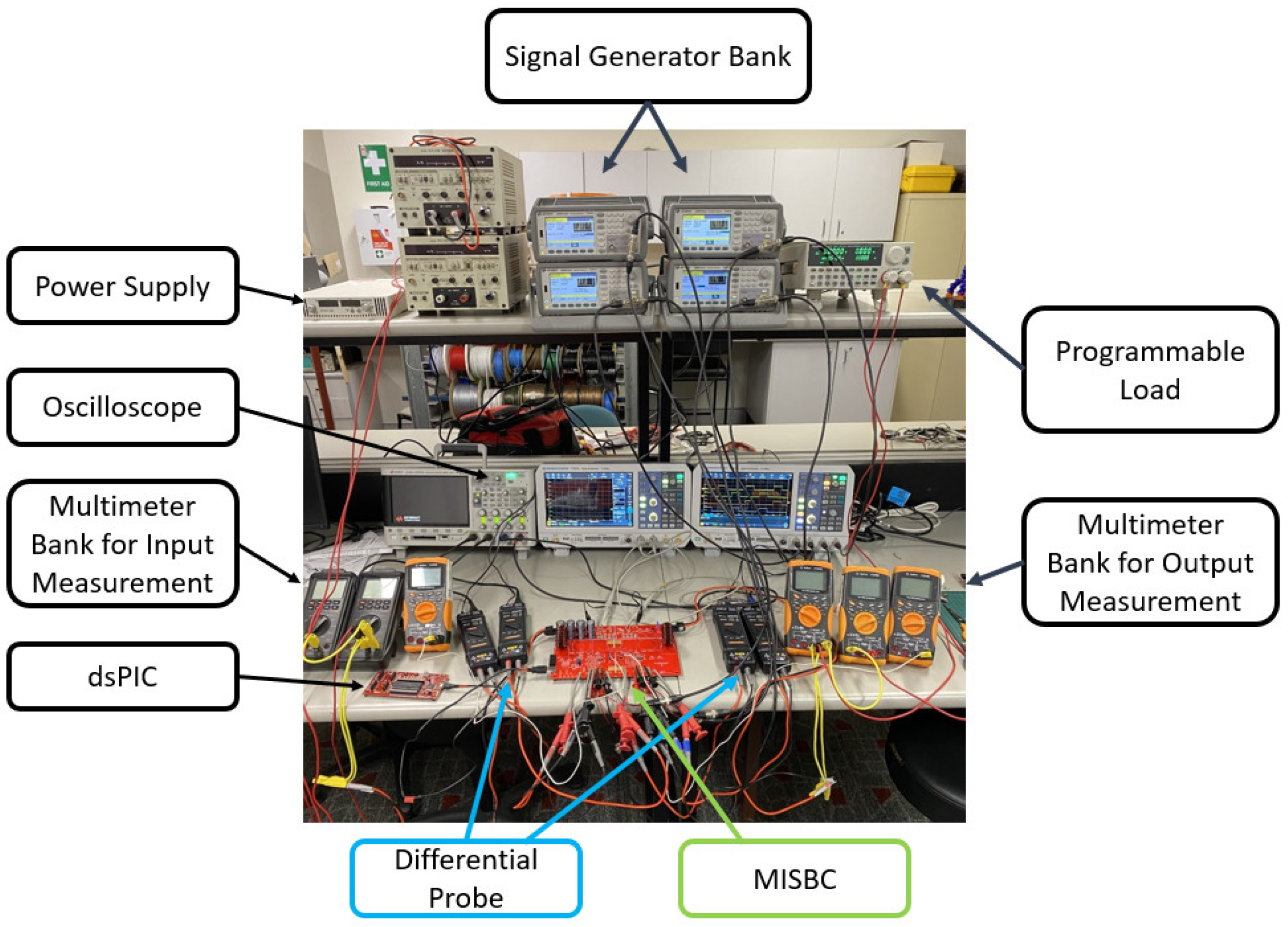
Figure 16.
Connections made to the prototype.
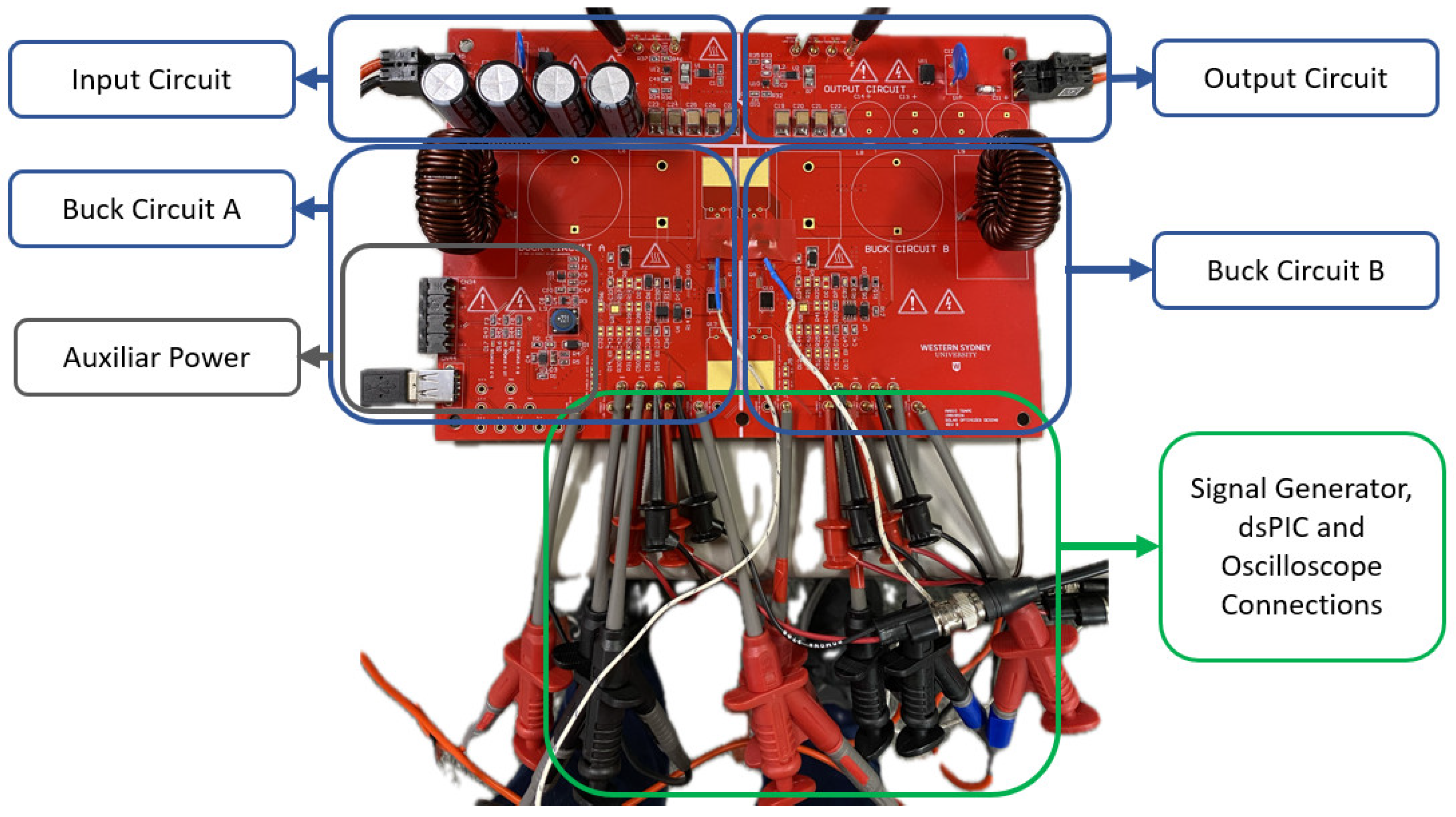
Figure 17.
Control diagram with dsPIC33.
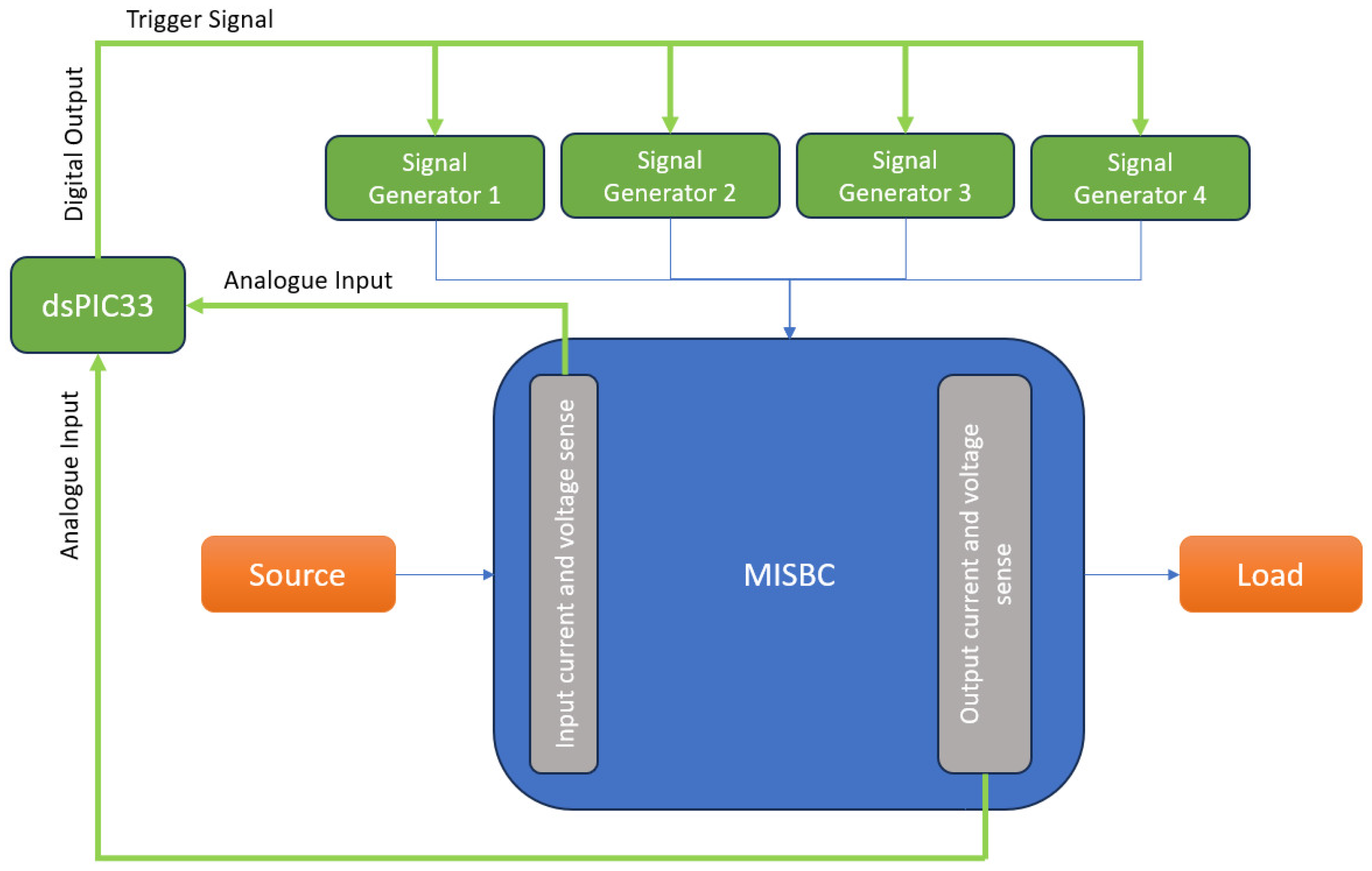
Figure 18.
(a) Generated signal from the signal generator bank, with an overshoot value of 13.9%; (b) Signal received from the gate driver, across the gate and source pins of the MOSFETs used on the half bridge configuration, with an overshoot of 19%.
Figure 18.
(a) Generated signal from the signal generator bank, with an overshoot value of 13.9%; (b) Signal received from the gate driver, across the gate and source pins of the MOSFETs used on the half bridge configuration, with an overshoot of 19%.
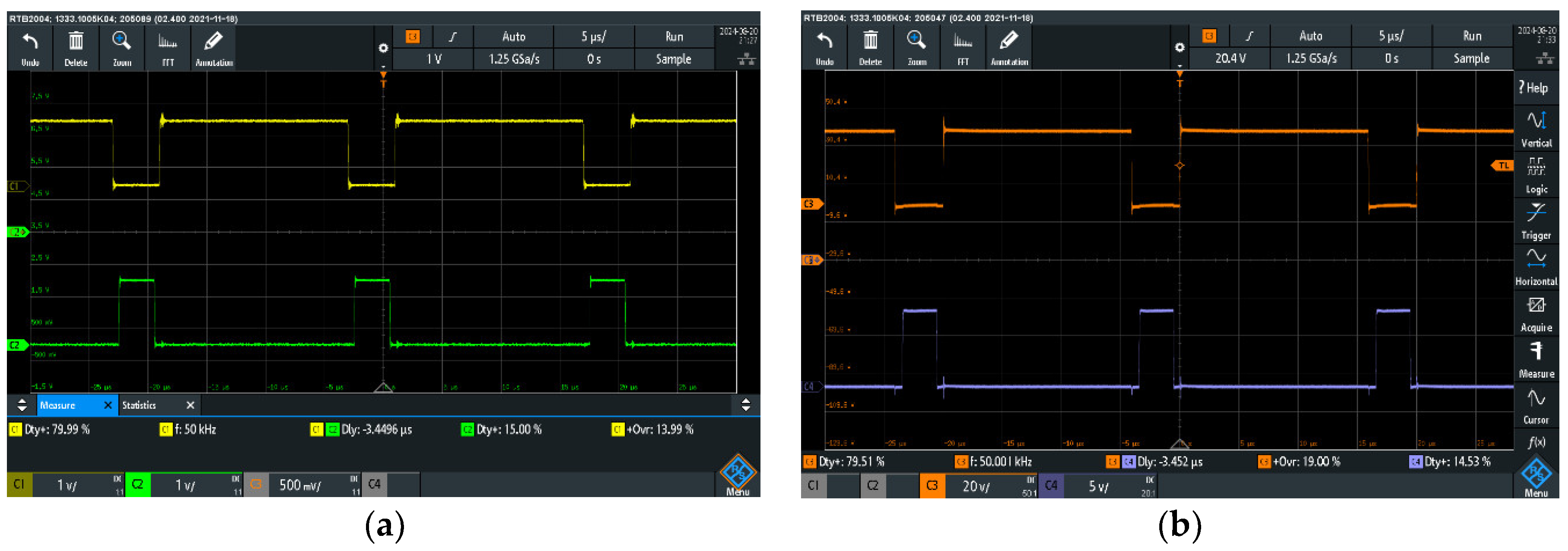
Figure 19.
(a) Signal received across the gate and source pins of the MOSFETs, when duty cycle was 26.38%, resulting in an overshoot of 23.52%; (b) Signal received across the gate and source pins of the MOSFETs, when duty cycle was 47.74%, resulting in an overshoot of 37.24%.
Figure 19.
(a) Signal received across the gate and source pins of the MOSFETs, when duty cycle was 26.38%, resulting in an overshoot of 23.52%; (b) Signal received across the gate and source pins of the MOSFETs, when duty cycle was 47.74%, resulting in an overshoot of 37.24%.
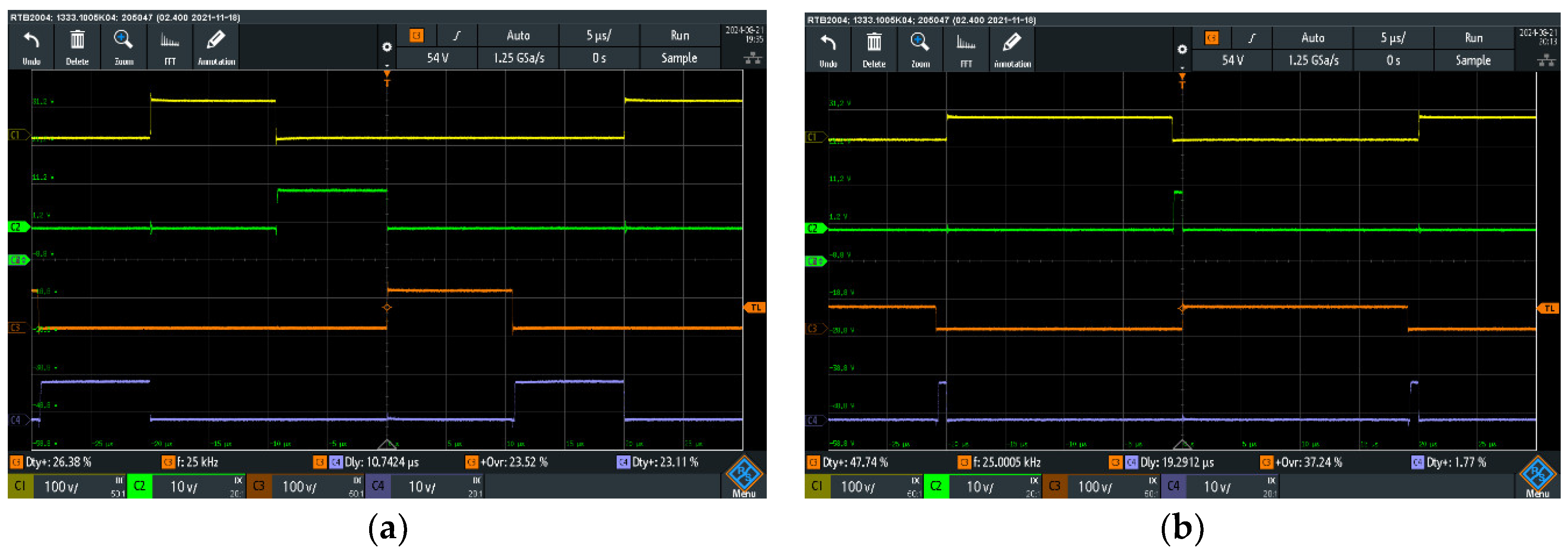
Figure 20.
Efficiency results from the MISBC during Prototype evaluation.
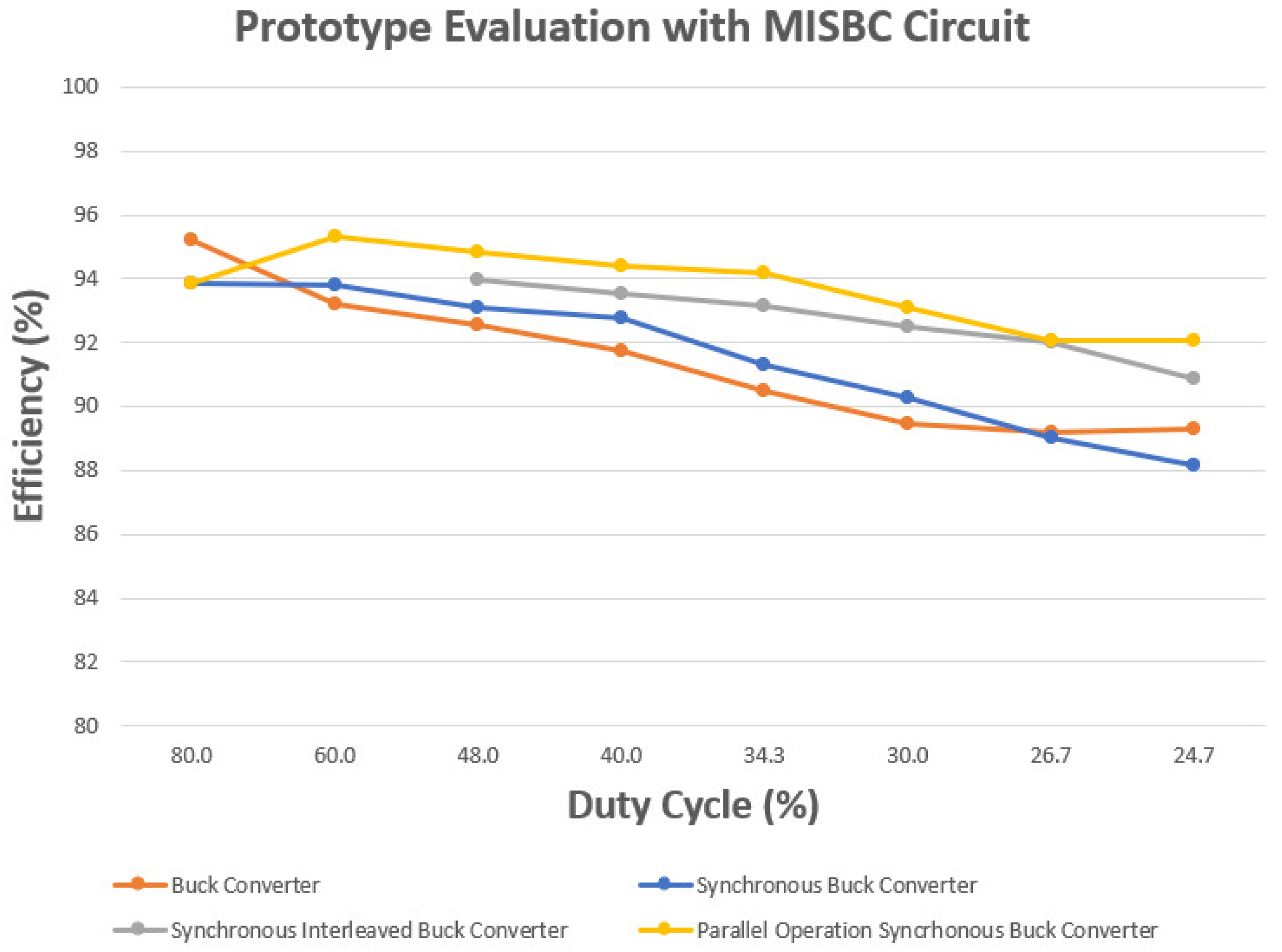
Figure 21.
Output voltage achieved during MISBC prototype evaluation.
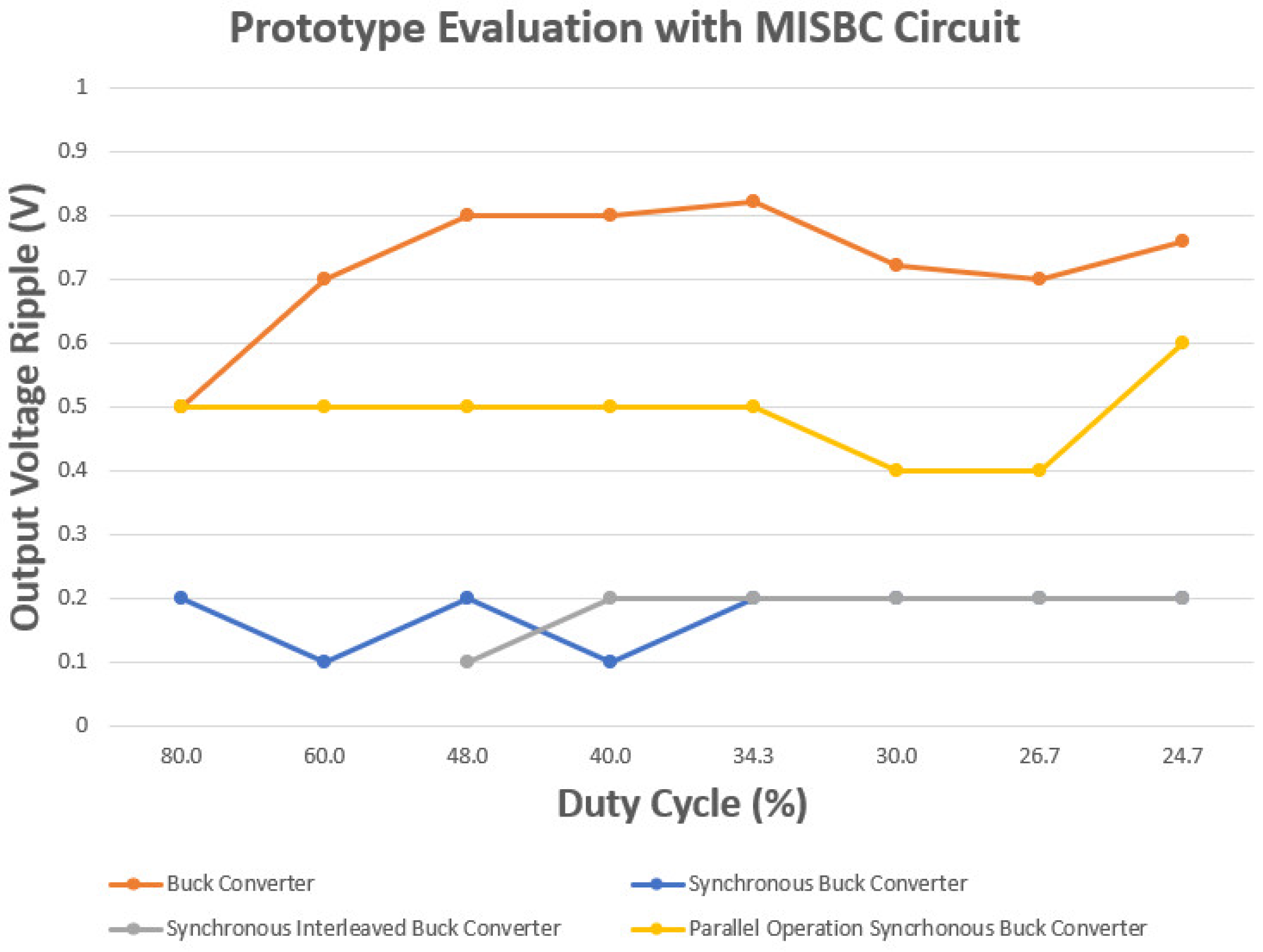
Figure 22.
Output voltage range achieved during MISBC Prototype evaluation.
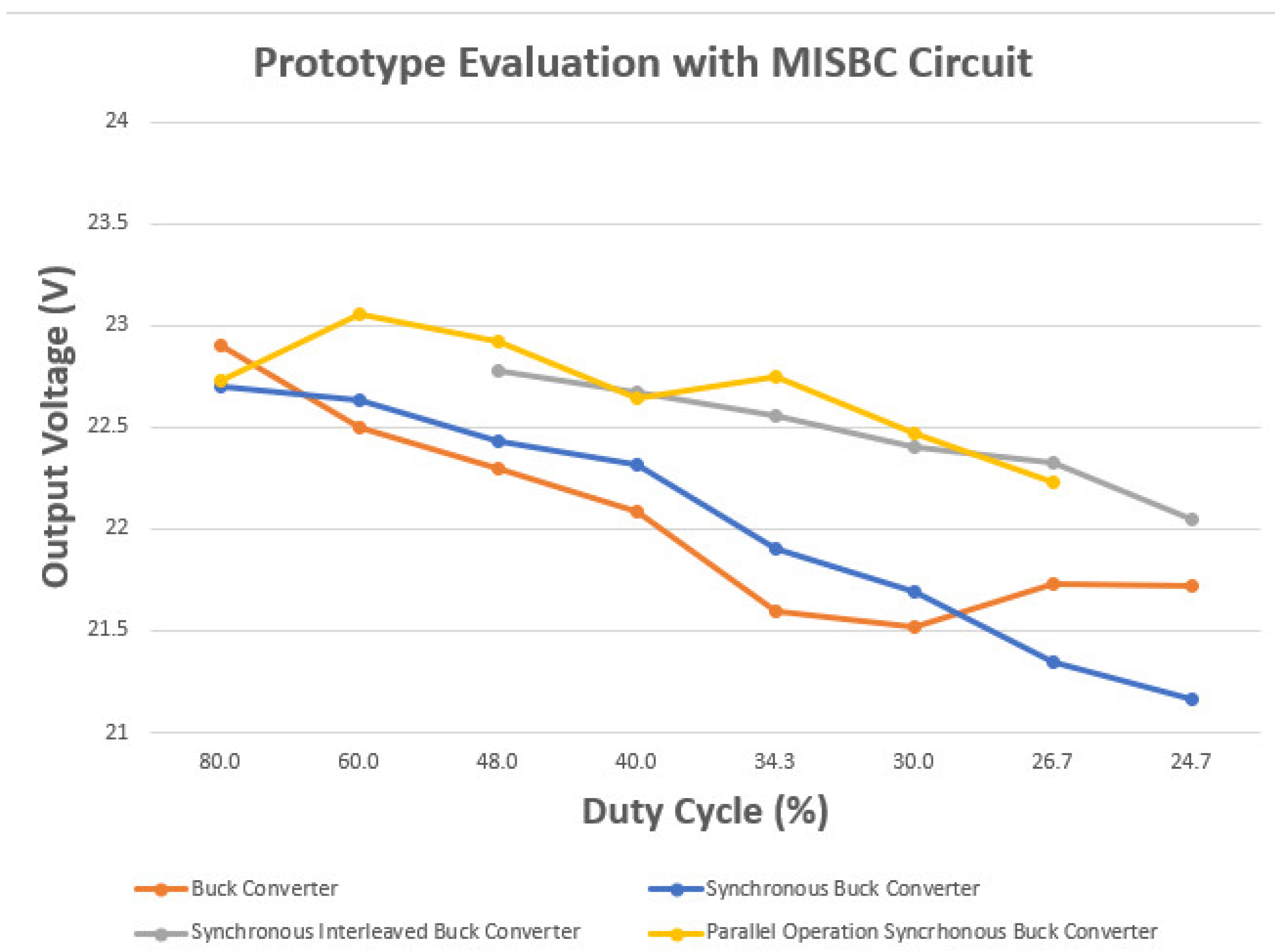
Figure 23.
Temperature rise of the High Side MOSFET Q1, during the MISBC prototype evaluation.
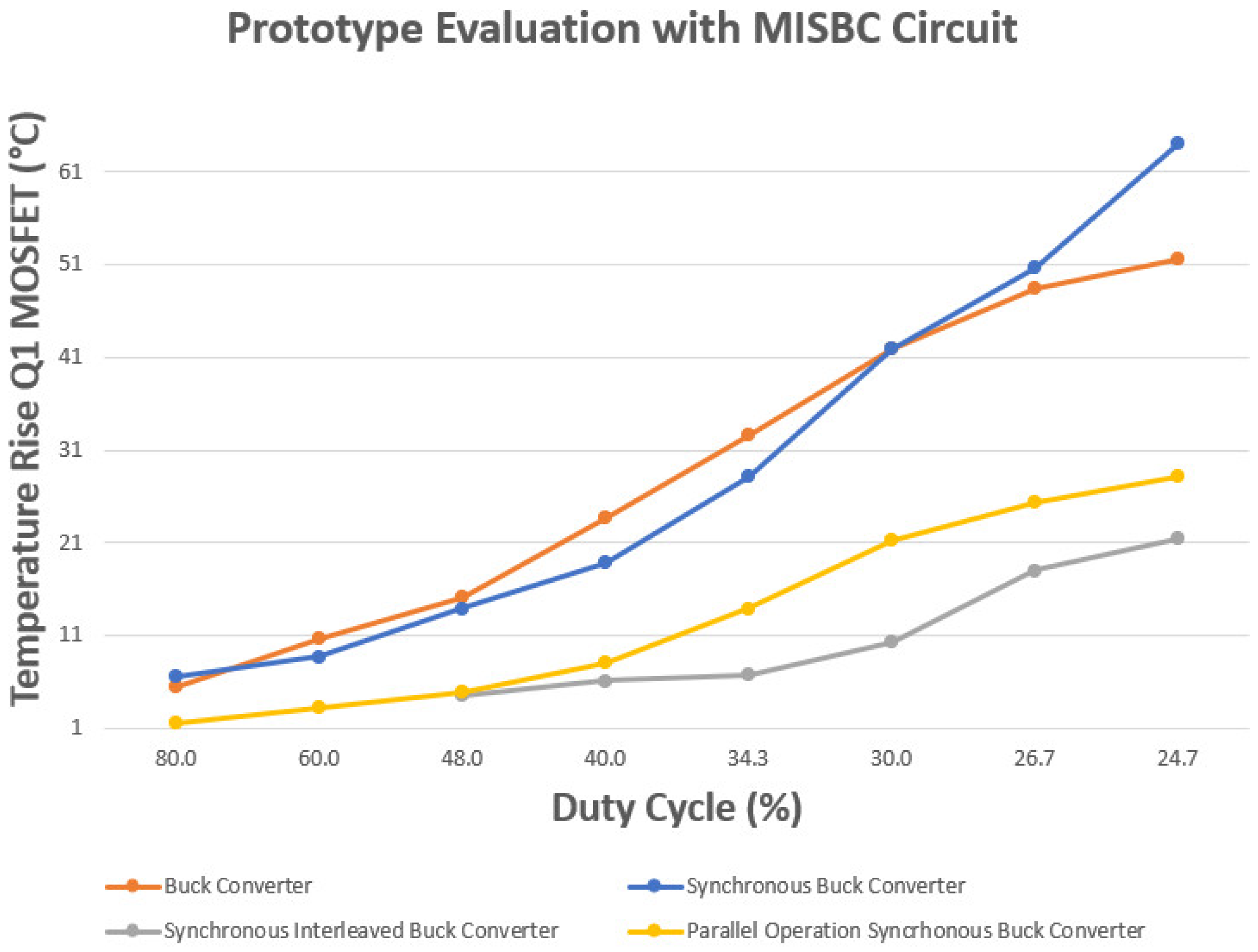
Figure 24.
Efficiency results from the MISBC during Prototype evaluation with a trendline based on second order polynomial equation.
Figure 24.
Efficiency results from the MISBC during Prototype evaluation with a trendline based on second order polynomial equation.
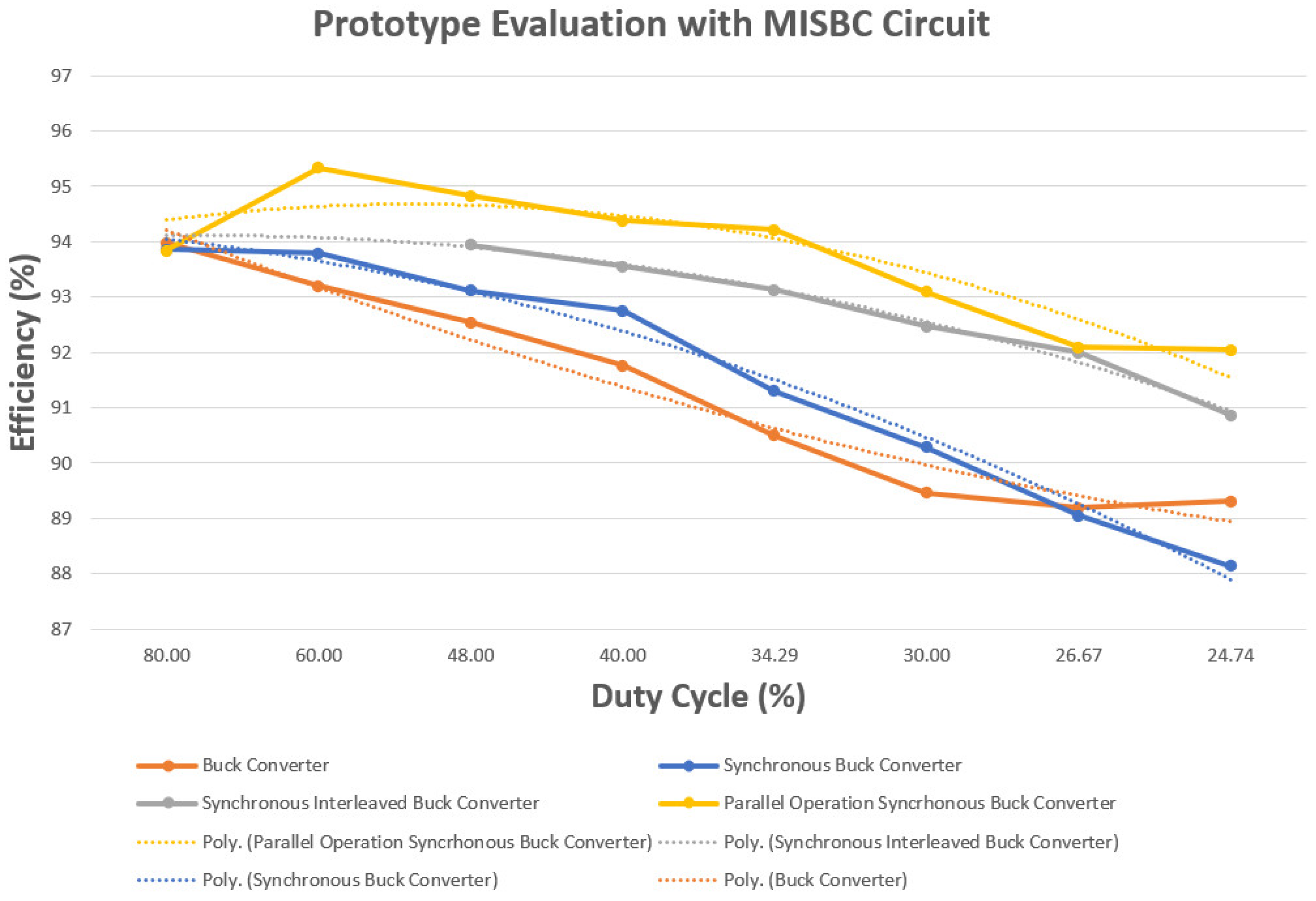
Table 1.
MOSFET Characteristics.
| Specification | IRF530N |
|---|---|
| RDS (on) at 25°C | 90 mΩ |
| Tj (Max) | 175 °C |
| RΘJA | 62 °C/W |
| VDS | 100 V |
| CRSS | 19 pF |
| ID | 17 A |
| Qg | 37 nC |
| PD. | 70 W |
Table 2.
Gate driver characteristics.
| Specification | LM5109 |
|---|---|
| VHB to VSS. | 0 to 118 V |
| RΘJA | 160 °C/W |
| Tj (Max) | 150 °C |
| tHPHL at 25°C | 27 ns |
| tLPLH at 25°C | 29 ns |
Table 7.
Efficiency comparison between MISBC circuit and Mean Well DDR-240 Series.
| (V) | ||
|---|---|---|
| DDR-240C-24 | 48 | 92.5 |
| DDR-240D-24 | 67.2 | 92.5 |
| Topology 1 | 50 | 92.5 |
| Topology 1 | 70 | 90.5 |
| Topology 2 | 50 | 93.1 |
| Topology 2 | 70 | 91.3 |
| Topology 3 | 50 | 93.9 |
| Topology 3 | 70 | 93.2 |
| Topology 4 | 50 | 94.8 |
| Topology 4 | 70 | 94.2 |
Disclaimer/Publisher’s Note: The statements, opinions and data contained in all publications are solely those of the individual author(s) and contributor(s) and not of MDPI and/or the editor(s). MDPI and/or the editor(s) disclaim responsibility for any injury to people or property resulting from any ideas, methods, instructions or products referred to in the content. |
© 2024 by the authors. Licensee MDPI, Basel, Switzerland. This article is an open access article distributed under the terms and conditions of the Creative Commons Attribution (CC BY) license (http://creativecommons.org/licenses/by/4.0/).
Copyright: This open access article is published under a Creative Commons CC BY 4.0 license, which permit the free download, distribution, and reuse, provided that the author and preprint are cited in any reuse.


