As is now well-understood, a solid understanding of the chemical and physical phenomena dictating the metal–semiconductor interfaces (MSIs) is imperative for an unerring realization of semiconductor devices [
1,
2]. Schottky–Mott rule, in its crude form, predicts that interfacing a high work function metal with a low work function n-type semiconductor will result in a Schottky barrier at the MSI [
3,
4]. Conversely, a Schottky barrier can also be expected at the interface formed between a low work function metal and a high work function p-type semiconductor [
5,
6]. While the existence of such barriers is a requirement for some device applications [
7], it can be undesirable for others [
1,
8]. Therefore, selecting the right combination of metals and semiconductors for the desired application necessitates an unerring characterization of the MSI of interest. This is where X-ray photoelectron spectroscopy (XPS) comes in handy: it is often used for a systematic investigation of the MSI wherein a series of metal-thickness dependent core-level photoemission spectra are collected and analyzed [
2,
6,
9,
10,
11,
12,
13,
14], and based on the metal-coverage dependent changes in the core-level binding energies, or lack thereof, the presence (or absence) of Schottky-barrier at the MSI is deduced [
2,
6,
11,
12,
13,
14,
15]. Besides such metal-thickness dependent spectroscopic measurements (see refs. [
2,
11,
12,
13,
14,
15,
16,
17,
18,
19,
20] for specific examples of clear signatures of band bending in obtained photoemission spectra), examining the electrical transport characteristics of electronic devices comprising the same metal–semiconductor assembly is another viable way for experimentally deciphering the true nature of interfacial phenomena at the MSI.
However, as is well-established, the simple Schottky–Mott model is anything but correct as it usually fails to explain the experimentally observed phenomena at the MSI due to multiple reasons discussed elsewhere [
2,
9,
21] and in the following paragraph. This should not come off as surprising since ideal theoretical models seldom help explain the experimental data entirely; nevertheless, this gives rise to a question of paramount importance, which now appears to be the elephant in the room. The all-important question is: can one always expect the results of XPS to show a clear correlation with the electrical transport measurements when studying a given MSI? Here, we intend to answer the above-mentioned question through a rigorous, multifactored, argument founded on the combination of fundamental interfacial physics and chemistry.
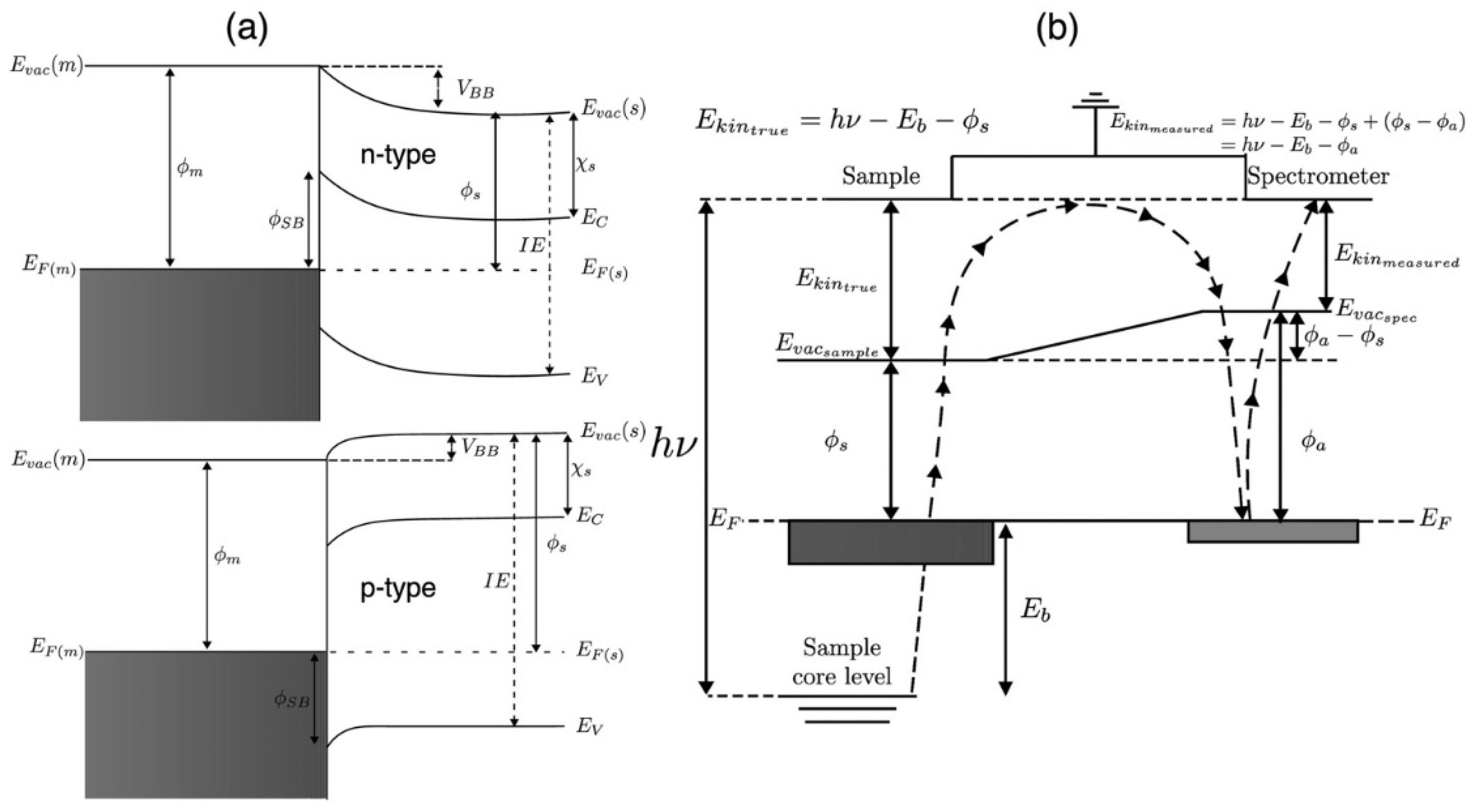
According to the simple Schottky–Mott model, when a high work function (Φ
M) metal is interfaced with a low work function n-type semiconductor (Φ
N) it leads to transfer of charges across the interface. This charge transfer, which is purely physical in nature, continues until the Fermi levels (E
F) match (top panel of
Figure 1a), resulting in a Helmholtz double layer due to induction of charges at the interface. So, in an ideal world free from any interfacial chemical interactions and complete electrical isolation from the ambience, the height of the n-type Schottky barrier (Φ
SBH-N) would be the difference between the work function of the metal and the electron affinity of the n-type semiconductor (
), i.e., Φ
SBH-N = Φ
M –
[
21,
22]. Likewise, the height of the p-type Schottky barrier (Φ
SBH-P) occurring at the interface between a low work function metal and a high function p-type semiconductor (Φ
P), under the ideal conditions (bottom panel of
Figure 1a), would be the difference between the work function of the metal and the ionization energy of the p-type semiconductor (
IEP), i.e., Φ
SBH-P =
IEP – Φ
M [
21,
22]. In the real world, however, things are way far away from the Schottky–Mott limit and these watered-down, generic, expressions for calculating the Schottky barrier heights fail in more than aspect as metal-induced gap states [
23,
24,
25], quasi-bonding-induced gap states [
26] and interfacial dipole due to the difference between Φ
M and Φ
N (or Φ
P) weigh in [
9,
21]. It must also be noted that since the cause behind the formation of the obtained double layer at the MSI is purely physical, in principle, it can be undone by getting rid of the accumulated charge at the MSI.
The ideal Schottky–Mott limit considers the metals and semiconductors to be semi-infinite but in reality none of these systems are semi-infinite, and since the dielectric constant of any given metal is extremely high, the charges accumulated at the interface (on the side of the metal) will redistribute themselves and accumulate at the surface of the metal far from the MSI. And this would be true as long as the metal–semiconductor assembly is electrically isolated. However, this may not always be the case when the metal contacts are thermally evaporated on top the semiconducting material for in situ XPS analysis, as the evaporated contacts might form thin blankets that will eventually establish good electrical contacts with the spectrometer. This is an extremely important point to consider as the samples and the spectrometer are usually grounded, with their Fermi levels aligned (see
Figure 1b), during a standard XPS measurement [
27]. In other words, depending on the kind of metal being evaporated on the surface of the semiconductor, the surface energy of the evaporated metal, and the degree of the coalescence of its islands, the band-bending and the expected Schottky barrier may disappear completely as the deposited metal makes a proper contact with the sample plate (as can be inferred from the green curves in Figure 3 of ref. [
14]). When the thickness of the Au contact in Figure 3 of ref. [
14] is increased to 0.8 nm, the binding energy of the S 2p and Zr 3d core levels return to their original values (i.e., the values in the absence of thermally evaporated Au on top of ZrS
3). This phenomenon would imply that the Schottky-barrier has vanished, and thus expecting an Ohmic Au/ZrS
3 interface would be a reasonable expectation. Nonetheless, the device characteristics reveal that the Au/ZrS
3 is far from Ohmic [
14]. Therefore, here, it is fair to say that had the device measurements in ref. [
14] been absent, the chances of conveying the true character of the Au/ZrS
3 interface, in an unequivocal manner, would have been low.
Moreover, due to the size of nanomaterials, which are being extensively investigated for their promising applications, the probability of occurrence of such a phenomenon is amplified even for lower metal thicknesses than usual. Therefore, adding extra complexity to the analysis of the metal thickness-dependent XPS spectra taken to unravel the nature of the MSI formed between a given metal and the nanomaterial of interest. Another crucial factor that cannot be overlooked, and adds further ordeal to the analysis of the metal thickness-dependent XPS, is the uncompensated charge in the semiconductor lattice resulting as a direct consequence of charge transfer across the MSI. The presence of uncompensated charge in the semiconductor lattice, right at the MSI, will strongly alter χ (and
IE) of the semiconductor at the MSI. Such an influence of Fermi-level alignment on the electronegativity and ionization energy of the semiconductor will, as one may expect, manifest itself as enhanced likelihood of interfacial chemical interactions at the MSI (as can be easily deciphered from [
2,
5,
14,
15,
28]). Analysis of the metal-coverage dependent XPS spectra could be hindered further in case one or more core levels of any of the elements, comprising the material of interest, overlap with any of the core levels of the thermally evaporated metal contact [
2,
18]. This is not all, because when it comes to analyzing core-level XPS spectra of metals, the databases referred for charge referencing purposes can be highly misleading as is reflected by a sizeable spread of ~3 eV in the reported binding energy values of a given core-level [
29]. Elaborately speaking, depending on the spatial and temporal coordinates of the conducted XPS experiments, the reported values of binding energy for a certain metallic core-level can vary by as much as 3 eV [
29]. Thus, any attempt aimed towards extracting a complete fundamental understanding of the MSI solely through the analysis of the metal thickness-dependent XPS data is inadvisable owing to misleading XPS databases [
29], and a myriad of cumbersome parameters whose knowledge prior to the data analysis is indispensable.
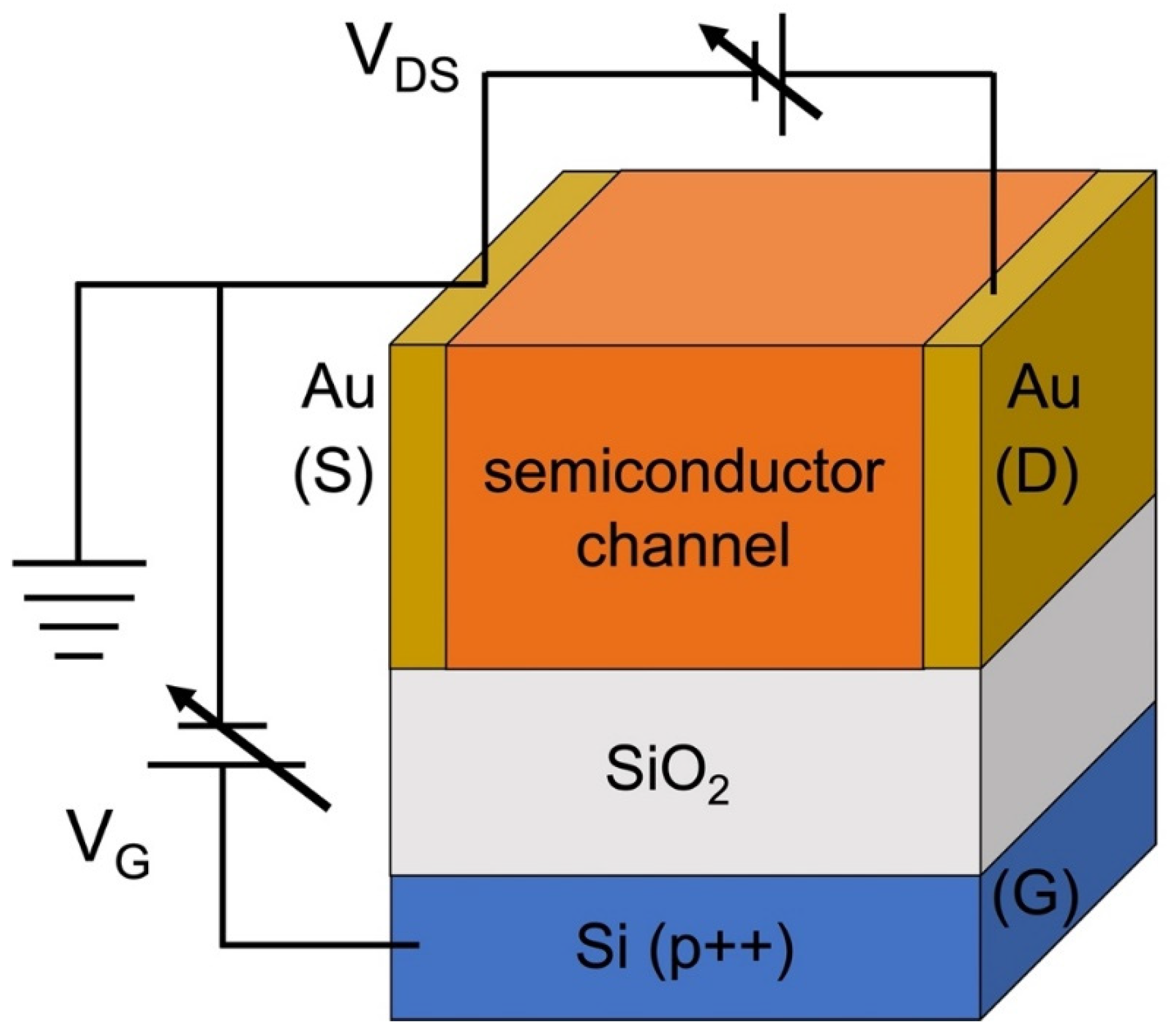
Nonetheless, there does exist a viable route to outmaneuver this scenario in order to look at the Schottky barriers at the MSI. This route involves fabricating three-terminal field-effect transistors (FETs) with the semiconductor of interest as the channel material [
2,
11,
12,
13,
14,
15,
16,
18,
30] (schematic shown in
Figure 2) and measuring the current–voltage characteristics (I–V characteristics) at zero gate bias (i.e., V
G = 0 V). Maintaining V
G = 0 V, while the drain-to-source voltage (V
DS) is changed, ensures that no additional states are added to the E
F. Hence, the MSI can be studied and the interfacial phenomenon can be eventually analyzed with relative ease, without any external perturbation to the intrinsic states at the MSI (various elaborate examples demonstrating the characterization of MSIs via this approach are contained in [
2,
5,
11,
12,
13,
14,
15,
16,
18,
30,
31]). For a purist, if a Schottky barrier does exist at the MSI it will manifest itself as a double Schottky barrier [
32,
33,
34,
35] in the I–V measurements of the FET based on the semiconductor of interest. Finally, for further clarification, we would like to add that the reason why XPS results may not always correlate with electrical transport measurements is because, sooner or later, the thermally evaporated contacts establish good electrical contacts with the spectrometer (as described in the preceding paragraph and can be reckoned from [
2,
14,
31]). Therefore, during the XPS measurements the metal–semiconductor assembly is not electrically isolated from its surroundings anymore. However, in the case of FETs, the metal–semiconductor assembly on top of the dielectric oxide is, by definition, electrically isolated. Another noteworthy difference between the XPS-assisted characterization and electrical characterization of the MSI is that they are essentially two quite different worlds to begin with, as the first method of characterization would generate an immense number of charges unlike the latter. And if the surface of the semiconductor of interest is highly insulating then the eventual attempt of decoupling the effect of surface charging effects [
29,
36], which result in shifting of core-level photoemission spectra towards higher binding energies, from the actual band bending would be anything but trivial.
In conclusion, it is evident that, for decades, the photoemission community all across the globe has been exploiting the strengths of XPS in order to gather fundamental physical and chemical insights into the metal–semiconductor interfaces. But just because something is a longstanding tradition does not make it flawless. Therefore, since not all the parameters required for accurate analyses of the metal-thickness dependent XPS data (obtained for the MSI of interest) are known a priori, its standalone use for such studies is discouraged. To circumvent a plethora of complexities that one may encounter while using core-level photoemission spectroscopy to understand the MSI [
14], characterization of the MSI via electrical transport measurements is recommended for extraction of unambiguous information about the same. Especially, if the eventual goal is to fabricate semiconductor-based electronics, there is all the more reason for the device transport measurements to take the center stage for the investigation of the MSI, relegating metal-thickness dependent XPS to a secondary position. Since the research in the area of semiconductors is currently transcending multiple science and engineering communities, the discussions presented herein are bound to alter the global status quo pertaining to semiconductor science and technology.
Acknowledgments
Archit Dhingra would like to acknowledge the financial support from the Spanish Ministry of Science and Innovation through “Severo Ochoa” (Grant CEX2020-001039-S), “María de Maeztu” (Grant CEX2018-000805-M) Programmes for Centres of Excellence in R&D, and the Comunidad de Madrid through (MAD2D-CM)-MRR MATERIALES AVANZADOS-IMDEA-NC. The authors are grateful to Prof. Grzegorz (Greg) Greczynski (IFM, Linköping University) for highly stimulating and useful discussions which have, undoubtedly, strengthened the message of this paper by polishing the quality of the arguments presented herein.
Conflicts of interest: There are no conflicts of interest to declare.
References
- D. S. Schulman, A. J. Arnold, and Saptarshi Das, Contact Engineering for 2D Materials and Devices, Chem Soc Rev 47, 3037 (2018). [CrossRef]
- A. Dhingra, D. E. Nikonov, A. Lipatov, A. Sinitskii, and P. A. Dowben, What Happens When Transition Metal Trichalcogenides Are Interfaced with Gold?, J Mater Res 38, 52 (2023). [CrossRef]
- W. Schottky, Zur Halbleitertheorie Der Sperrschicht- Und Spitzengleichrichter, Zeitschrift Für Physik 113, 367 (1939). [CrossRef]
- N. F. Mott, The Theory of Crystal Rectifiers, Proceedings of the Royal Society A 171, 153 (1939). [CrossRef]
- A. Dhingra, A. Lipatov, M. J. Loes, J. Abourahma, M. Pink, A. Sinitskii, and P. A. Dowben, Effect of Au/HfS3 Interfacial Interactions on Properties of HfS3-Based Devices, Physical Chemistry Chemical Physics 24, 14016 (2022). [CrossRef]
- Z. Zhang and J. T. Yates, Band Bending in Semiconductors: Chemical and Physical Consequences at Surfaces and Interfaces, Chem Rev 112, 5520 (2012). [CrossRef]
- J. R. Waldrop and R. W. Grant, Interface Chemistry of Metal-GaAs Schottky-Barrier Contacts, Appl Phys Lett 34, 630 (1979). [CrossRef]
- S. Chen, S. Wang, C. Wang, Z. Wang, and Q. Liu, Latest Advance on Seamless Metal-Semiconductor Contact with Ultralow Schottky Barrier in 2D-Material-Based Devices, Nano Today 42, 101372 (2022). [CrossRef]
- Y. Gao, Surface Analytical Studies of Interfaces in Organic Semiconductor Devices, Materials Science and Engineering: R: Reports 68, 39 (2010). [CrossRef]
- K. Horn, Semiconductor Interface Studies Using Core and Valence Level Photoemission, Applied Physics A Solids and Surfaces 51, 289 (1990). [CrossRef]
- G. Viswan, K. Wang, R. Streubel, X. Hong, N. Valanoor, D. Sando, and P. A. Dowben, Magnetocapacitance at the Ni/BiInO3 Schottky Interface, ACS Appl Mater Interfaces 16, 4108 (2024). [CrossRef]
- N. Wu, Z. Xing, L. Luo, and G. Li, Normally-off GaON/p-GaN Gate HEMTs with Selective Plasma Oxidation: From Structural Characterization, Performance Improvement to Physical Mechanism, Semicond Sci Technol 39, 045015 (2024). [CrossRef]
- M.-Y. Kim, D.-W. Byun, G.-H. Lee, S. Pookpanratana, Q. Li, and S.-M. Koo, Schottky Barrier Heights and Electronic Transport in Ga2O3 Schottky Diodes, Mater Res Express 10, 075902 (2023). [CrossRef]
- A. Dhingra, A. Lipatov, A. Sinitskii, and P. A. Dowben, Complexities at the Au/ZrS3(001) Interface Probed by x-Ray Photoemission Spectroscopy, Journal of Physics: Condensed Matter 33, 434001 (2021). [CrossRef]
- S. J. Gilbert, A. Lipatov, A. J. Yost, M. J. Loes, A. Sinitskii, and P. A. Dowben, The Electronic Properties of Au and Pt Metal Contacts on Quasi-One-Dimensional Layered TiS3(001), Appl Phys Lett 114, 101604 (2019). [CrossRef]
- D. Caliskan, H. Sezen, E. Ozbay, and S. Suzer, Chemical Visualization of a GaN P-n Junction by XPS, Sci Rep 5, 14091 (2015). [CrossRef]
- S. Schuwalow et al., Band Structure Extraction at Hybrid Narrow-Gap Semiconductor–Metal Interfaces, Advanced Science 8, (2021). [CrossRef]
- A. Dhingra et al., Surface Termination and Schottky-Barrier Formation of In4Se3(001), Semicond Sci Technol 35, 065009 (2020). [CrossRef]
- L. A. M. Lyle, T. C. Back, C. T. Bowers, A. J. Green, K. D. Chabak, D. L. Dorsey, E. R. Heller, and L. M. Porter, Electrical and Chemical Analysis of Ti/Au Contacts to β -Ga2O3, APL Mater 9, 061104 (2021). [CrossRef]
- L. A. M. Lyle, Critical Review of Ohmic and Schottky Contacts to β-Ga2O3, Journal of Vacuum Science & Technology A 40, (2022). [CrossRef]
- R. T. Tung, The Physics and Chemistry of the Schottky Barrier Height, Appl Phys Rev 1, (2014). [CrossRef]
- Y. Liu, Q. Zhang, W. Zhang, R. Zhang, B. Wang, C. Ji, Z. Pei, and S. Sang, Tuning Schottky Barrier and Contact Type of Metal–Semiconductor in Ti3C2T2/MoS2 (T = F, O, OH) by Strain: A First-Principles Study, The Journal of Physical Chemistry C 125, 16200 (2021). [CrossRef]
- D. Wang, C. Tan, S. Wang, Z. Yang, L. Yang, and Z. Wang, Sm and Gd Contacts in 2D Semiconductors for High-Performance Electronics and Spintronics, ACS Appl Mater Interfaces 16, 14064 (2024). [CrossRef]
- T. Nishimura, K. Kita, and A. Toriumi, Evidence for Strong Fermi-Level Pinning Due to Metal-Induced Gap States at Metal/Germanium Interface, Appl Phys Lett 91, (2007). [CrossRef]
- S. Li, J. Chen, X. He, Y. Zheng, C. Yu, and H. Lu, Comparative Study of the Micro-Mechanism of Charge Redistribution at Metal-Semiconductor and Semimetal-Semiconductor Interfaces: Pt(Ni)-MoS2 and Bi-MoS2(WSe2) as the Prototype, Appl Surf Sci 623, 157036 (2023). [CrossRef]
- L.-X. Zhou et al., Quasi-Bonding-Induced Gap States in Metal/Two-Dimensional Semiconductor Junctions: Route for Schottky Barrier Height Reduction, Phys Rev B 105, 224105 (2022). [CrossRef]
- G. Greczynski and L. Hultman, A Step-by-Step Guide to Perform x-Ray Photoelectron Spectroscopy, J Appl Phys 132, (2022). [CrossRef]
- A. Dhingra, Physical and Electronic Properties of Two-Dimensional Layered Materials: In4Se3, TiS3, ZrS3, HfS3, and GeI2, University of Nebraska-Lincoln, 2022.
- G. Greczynski and L. Hultman, X-Ray Photoelectron Spectroscopy: Towards Reliable Binding Energy Referencing, Prog Mater Sci 107, 100591 (2020). [CrossRef]
- A. Dhingra, P. A. Dowben, A. Lipatov, and A. Sinitskii, HfS3 FIELD-EFFECT TRANSISTORS WITH A TWO-DIMENSIONAL HOLE GAS, US-20240162342-A1 (16 May 2024).
- S. J. Gilbert et al., Effect of Band Symmetry on Photocurrent Production in Quasi-One-Dimensional Transition-Metal Trichalcogenides, ACS Appl Mater Interfaces 12, 40525 (2020). [CrossRef]
- C. Cheng, J. He, and J. Hu, Naturally Asymmetrical Double-Schottky Barrier Model: Based on Observation of Bicrystal, Appl Phys Lett 101, (2012). [CrossRef]
- Q. Wang, C. Liu, B. Ma, Y. Gao, M. Fitzpatrick, Y. Li, B. Liu, C. Gao, and Y. Ma, High Pressure Study of B12As2: Electrical Transport Behavior and the Role of Grain Boundaries, J Appl Phys 117, (2015). [CrossRef]
- A. Grillo and A. Di Bartolomeo, A Current–Voltage Model for Double Schottky Barrier Devices, Adv Electron Mater 7, (2021). [CrossRef]
- Z. Cheng, Z. Hou, Y. Wang, M. Guo, K. Wu, J. Li, and Y. Lin, Steadily Decreasing Power Loss of a Double Schottky Barrier Originating from the Dynamics of Mobile Ions with Stable Interface States, Phys Rev Appl 17, 034042 (2022). [CrossRef]
- E. Echeverría, G. Peterson, B. Dong, S. Gilbert, A. Oyelade, M. Nastasi, J. A. Kelber, and P. A. Dowben, Band Bending at the Gold (Au)/Boron Carbide-Based Semiconductor Interface, Zeitschrift Für Physikalische Chemie 232, 893 (2018). [CrossRef]
|
Disclaimer/Publisher’s Note: The statements, opinions and data contained in all publications are solely those of the individual author(s) and contributor(s) and not of MDPI and/or the editor(s). MDPI and/or the editor(s) disclaim responsibility for any injury to people or property resulting from any ideas, methods, instructions or products referred to in the content. |
© 2025 by the authors. Licensee MDPI, Basel, Switzerland. This article is an open access article distributed under the terms and conditions of the Creative Commons Attribution (CC BY) license (http://creativecommons.org/licenses/by/4.0/).