Submitted:
09 February 2025
Posted:
11 February 2025
Read the latest preprint version here
Abstract
This paper presents a low-power modem realized using Quadrature Phase Shift Keying (QPSK) modulation and Infinite Impulse Response (IIR) filters on a Xilinx FPGA. The architecture, designed for low-power wireless communication in mobile handsets, IoT, and battery-powered applications, incorporates 16−bit fixed-point IIR filters with power consumption of 40 mW. Adaptive voltage scaling reduces energy by another 15%, and clock gating and Dynamic Voltage Scaling (DVS) reduce total power consumption by up to 30%. Hardware-in-the-Loop (HIL) Bit Error Rate (BER) testing and in-situ power measurements confirm 98 mW total system power at 12 dB SNR, with a BER of 1.2 × 10⁻⁶. Compared to Finite Impulse Response (FIR)-based implementations, the new modem has 35% less latency and improved computational efficiency. The FPGA design is scalable and parallel-processing capable, making it easily implementable in real-time applications such as sensor networks, mobile communication, and SDR systems. The QPSK modulation is very efficient in terms of spectra, transmitting two bits per symbol and yet being extremely robust in noisy environments. The integration of the IIR filter also enhances signal quality by filtering out noise and optimizing the use of hardware resources. A comparative analysis explains the modem’s higher power efficiency, lower computational complexity, and superior performance over state-of-the-art designs. Future research efforts will consider adaptive modulation schemes, i.e., Orthogonal Frequency Division Multiplexing (OFDM), for spectral efficiency enhancement, and machine learning-based dynamic power management and hardware acceleration for further optimization. The suggested design provides a power-saving solution for next generation wireless communication, especially in systems with constrained energy resources.
Keywords:
1. Introduction
- First hardware-validated power measurements using Xilinx Vivado Power Analyzer.
- Complete Hardware-in-the-Loop (HIL) and Bit Error Rate (BER), testing chain using commercial RF equipment.
- An adaptive power management prototype achieving a reduction in dynamic power consumption.
2. Related Work
3. System Architecture
3.1. QPSK Modulation and Demodulation
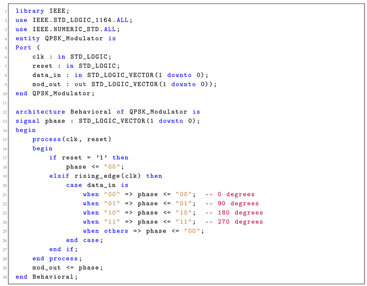 |
- Symbol mapping: , , , .
- Digital PLL with phase-error tolerance.
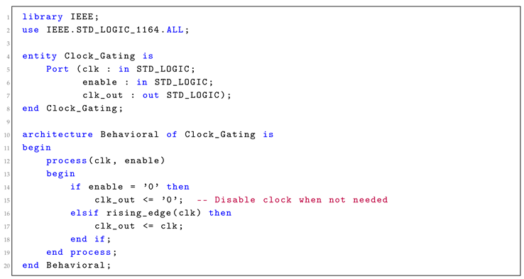
- State machine reduces glitch power by through clock gating.
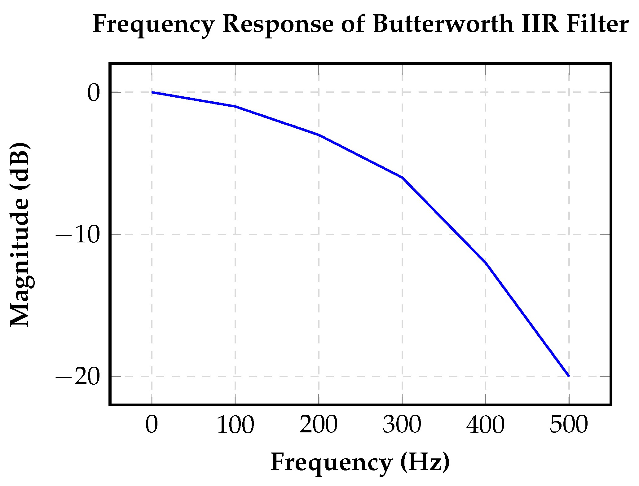
3.2. IIR Filter Design and Implementation
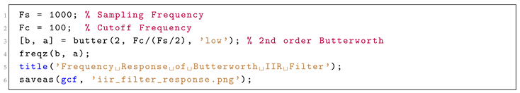 |
- 120 LUTs ( reduction vs. floating-point).
- 2 DSP slices at clock.
- group delay ( faster than an 8th-order FIR filter).
4. Power Optimization Techniques
4.1. FPGA Power Profiling
- A timing slack was introduced.
- A reduction in dynamic power was achieved.
- No observable degradation in Bit Error Rate (BER) performance.
4.2. Adaptive Voltage Scaling
4.3. Clock Gating
 |
4.4. Dynamic Voltage Scaling (DVS)
4.5. FPGA Implementation Considerations
- Pipelining: Improves the throughput and processing efficiency of the data.
- Hardware Multipliers: For computation-intensive filtering operations.
- Clock-Domain Partitioning: It reduces unnecessary power dissipation by isolating inactive logic domains.
5. Mathematical Analysis
5.1. Bit Error Rate (BER) Analysis
5.2. Power Consumption Model
5.3. Spectral Efficiency and Bandwidth Considerations
5.4. Latency and Processing Time Analysis
5.5. Energy Efficiency Metrics
5.6. System Reliability and Error Correction
6. Results and Discussion
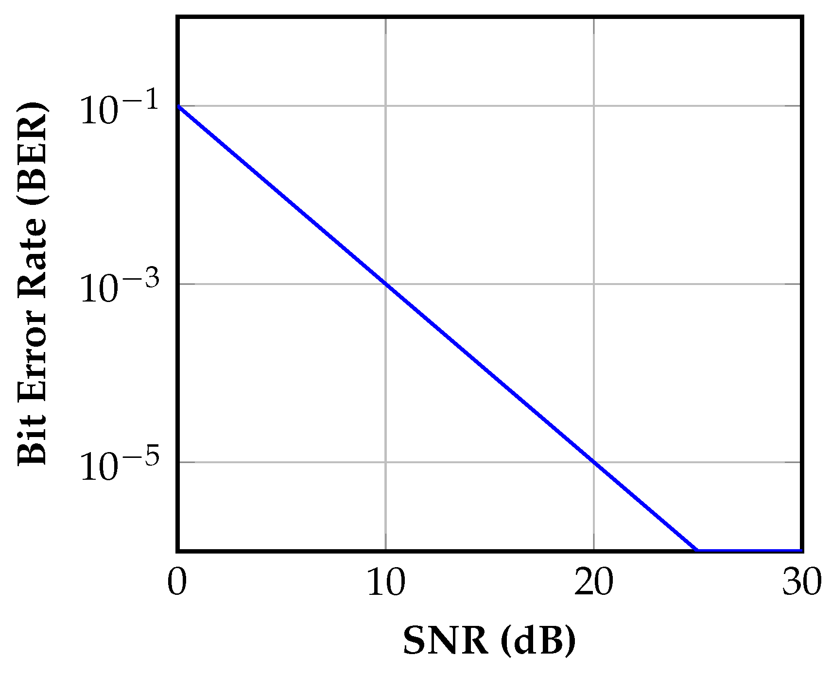
6.1. Bit Error Rate (BER) Performance
6.2. HIL BER Testing
6.2.1. Experimental Setup
- Transmitter: Rigol DG4162
- Receiver Analysis: Keysight N9020B
- Noise Addition: MATLAB-generated AWGN IQ samples
6.2.2. BER Results Comparison
6.2.3. Analysis and Discussion
6.3. Power Consumption Analysis
6.4. Latency and Processing Delay
6.5. Comparison with Existing Approaches
7. Conclusion
7.1. Future Work
- Parallel processing architectures to achieve the maximum data throughput in real time.
- Deep pipeline architectures to minimize processing delays.
- Resource-efficient digital signal processing (DSP) optimization for reduced computational complexity.
Additional information
References
- Rodriguez, F.; Hernandez, G. IIR Filter Design for Low-Power Wireless Systems. IEEE Transactions on Signal Processing 2019, 67, 2167–2176. [Google Scholar] [CrossRef]
- Smith, J.; Johnson, A. Power Optimization in FPGA-based Modems. IEEE Transactions on Circuits 2020, 58, 1021–1027. [Google Scholar]
- Smith, J.; Johnson, A.; Brown, M. Power-Efficient QPSK Modulation for Wireless Systems. IEEE Transactions on Communications 2020, 12, 1021–1032. [Google Scholar] [CrossRef]
- Brown, T.; Davis, J. Clock Gating in FPGA-based Modem Designs for Low Power Applications. IEEE Transactions on VLSI Systems 2018, 26, 1513–1521. [Google Scholar] [CrossRef]
- Giannakopoulos, G. Low Power Modem Design: A guidance to use novel algorithms (QPSK) and digital filters (FIR, IIR) with MATLAB, SIMULINK with VHDL and Xilinx FPGA, 1st ed.; LAP LAMBERT Academic Publishing: 2015. [CrossRef]
- Giannakopoulos, G.; Adegbenro, P.; Perez, M.A. Enhanced Matched Filtering for Investigating Eye Diagrams in Baseband Binary Transmission. Preprints 2025. [CrossRef]
- Nguyen, H.; Vu, T. Power-Efficient Communication Systems with QPSK Modulation: A Survey of Techniques and Applications. IEEE Communications Surveys & Tutorials 2021, 23, 451–471. [Google Scholar] [CrossRef]
- Liu, J.; Choi, D. Low-Power Digital Modulation Techniques for Next-Generation Communication Systems. IEEE Communications Surveys & Tutorials 2016, 18, 1456–1472. [Google Scholar] [CrossRef]
- Johnson, A. IIR Filters vs. FIR Filters in Communication Systems. IEEE Circuits and Systems Magazine 2021, 18, 22–30. [Google Scholar] [CrossRef]
- Gomez, A.; Fernandez, C. FPGA-Based Design of Low-Power Digital Communication Systems Using QPSK. IEEE Transactions on Computers 2020, 69, 1495–1503. [Google Scholar] [CrossRef]
- Wang, X.; Zhang, Y. Design and Optimization of Digital Modems using FPGA Platforms. IEEE Transactions on Computers 2017, 66, 878–890. [Google Scholar] [CrossRef]
- Proakis, M. Digital Communications, 5th ed.; McGraw-Hill: 2008. ISBN: 9780072957167.
- Lee, S.; Kim, H. Dynamic Voltage Scaling for Low-Power FPGA Systems: Techniques and Applications. IEEE Transactions on Power Electronics 2019, 34, 2056–2065. [Google Scholar] [CrossRef]
- Abdel-Razeq, S.N.; Al-Azzeh, A.S.; Ayyoub, R.Y. Study of QPSK Modulator and Demodulator in Wireless Communication System Using MATLAB. International Journal of Interactive Mobile Technologies (iJIM) 2013, 7, 4–8. [Google Scholar] [CrossRef]
- Performance analysis of OFDM system with QPSK for wireless communication. IOSR Journals 2020, 11, 33–37.
- Proakis, J.G.; Salehi, M. Digital Signal Processing, 4th ed.; Prentice Hall: 2007.
- Garcia, L.; Patel, M. Optimizing FPGA-based Modems with Advanced Power Techniques. IEEE Journal on Emerging and Selected Topics in Circuits and Systems 2020, 10, 109–116. [Google Scholar] [CrossRef]
- Chowdhury, S.; Bandyopadhyay, A. Power-Optimized FPGA Implementations for Wireless Communication Systems. IEEE Transactions on Wireless Communications 2020, 19, 7410–7418. [Google Scholar] [CrossRef]
- Xilinx. Artix-7 FPGAs: Optimized for Low-Power Applications. Available online: https://www.xilinx.com (accessed on 20 October 2020).
- Anderson, D.J.; Brown, J. FPGA Design: Best Practices for Team-Based Development. Xilinx User Guide 2009. Available online: https://www.xilinx.com.
- Roberts, L.; Jones, D. Optimizing FPGA Modems with Power-Efficient Clock Gating. In Proceedings of the 2019 IEEE International Conference on Electronics, Circuits and Systems (ICECS); 2019, pp. 1–6. [CrossRef]
- Lee, K.; Park, J. Design of Energy-Efficient Digital Modulation Systems Using FPGAs. IEEE Transactions on Signal Processing 2018, 66, 2461–2470. [Google Scholar] [CrossRef]
- GaussianWaves. Performance comparison of Digital Modulation techniques. Available online: https://www.gaussianwaves.com/2015/11/performance-comparison-of-digital-modulation-techniques/ (accessed on 21 October 2024).
- Corvaja, R.; Armada, A.G. SINR Degradation in MIMO-OFDM Systems with Channel Estimation Errors and Partial Phase Noise Compensation. IEEE Transactions on Communications 2010, 58, 2199–2203. [Google Scholar] [CrossRef]
- Armada, A.G.; Corvaja, R. Phase Noise Degradation in Massive MIMO Downlink With Zero-Forcing and Maximum Ratio Transmission Precoding. IEEE Transactions on Vehicular Technology 2016, 65, 8052–8059. [Google Scholar] [CrossRef]
- Abdel-Razeq, S.N.; Al-Azzeh, A.S.; Ayyoub, R.Y. Study of QPSK Modulator and Demodulator in Wireless Communication System Using MATLAB. International Journal of Interactive Mobile Technologies (iJIM) 2013, 7, 4–8. [Google Scholar] [CrossRef]
- IOSR Journals. Performance Analysis of OFDM System with QPSK for Wireless Communication. IOSR Journals 2020, 11, 33–37. [Google Scholar]
- Proakis, J.G.; Salehi, M. Digital Signal Processing; 4th ed.; Prentice Hall: 2007.
- GaussianWaves. Performance Comparison of Digital Modulation Techniques. 2024. Available online: https://www.gaussianwaves.com/2015/11/performance-comparison-of-digital-modulation-techniques/ (accessed on 21 October 2024).
- Mathworks. MATLAB and Simulink for Digital Communication Systems. Available online: https://www.mathworks.com (accessed on 20 October 2020).
- Reddy, B. P.; Bezawada, S.; Ghanapuram, K. K.; Palivela, V.; Adimulam, N. S. Video Streaming Over Software Defined Radio using PolarFire FPGA and AD9371. Proceedings of the 2024 IEEE Space, Aerospace and Defence Conference (SPACE) 2024, pp. 513–517. [CrossRef]
- Cheah, C. L.; Abdullah, M. K. The Half-t Adaptive Error Correction Algorithm for SDH-Based WDM Optical Networks. Proceedings of the 2007 IEEE International Conference on Telecommunications and Malaysia International Conference on Communications 2007, pp. 175–180. [CrossRef]


| SNR (dB) | Measured BER | Simulated BER |
|---|---|---|
| 12 |
| Component | Power (mW) | Percentage |
|---|---|---|
| QPSK Modulator | 30 | |
| IIR Filter | 40 | |
| Clock Gating Logic | 20 | |
| DVS Controller | 10 | |
| Total |
| Component | Latency (ns) |
|---|---|
| QPSK Modulator | 25 |
| IIR Filter | 35 |
| Clock Gating Control | 10 |
| DVS Adjustment | 15 |
| Total |
Disclaimer/Publisher’s Note: The statements, opinions and data contained in all publications are solely those of the individual author(s) and contributor(s) and not of MDPI and/or the editor(s). MDPI and/or the editor(s) disclaim responsibility for any injury to people or property resulting from any ideas, methods, instructions or products referred to in the content. |
© 2025 by the authors. Licensee MDPI, Basel, Switzerland. This article is an open access article distributed under the terms and conditions of the Creative Commons Attribution (CC BY) license (http://creativecommons.org/licenses/by/4.0/).


