
Submitted:
10 February 2025
Posted:
10 February 2025
You are already at the latest version
Abstract
Microfluidic technology is an emerging interdisciplinary field that use micropipes to handle or manipulate tiny fluids in chemistry, fluid physics, microelectronics, new materials and biomedical engineering. As one of the rapid prototyping methods, three-dimensional (3D) printing technique with rapid and cost-effective and integrated molding characteristics has became one of the important manufacturing technologies of microfluidic chip. Polymethyl-methacrylate (PMMA), as an exceptional thermoplastic material, has found widespread application in the field of microfluidics. This paper presented a comprehensive process research on the fabrication of fused deposition modeling (FDM) 3D printing PMMA microfluidic chips (chips), encompassing finite element numerical analysis studies, orthogonal process parameter optimization experiments, and the application of 3D printing integrated microfluidic reactors in the reaction between copper ions and ammonia water. In the work, the thermal stress finite element model shown the printing platform temperature was a significant printing parameters to prevent warping and delamination in the 3D printing process. And a single printing molding technique was employed to fabricate microfluidic chips with square cross-sectional dimensions reduced to 200 μm, and the microchannels exhibited no clogging or leakage. The orthogonal experiment method of 3D printing PMMA microchannels was carried out, and the optimized printing parameters resulted in a reduction of the microchannel profile to Ra 1.077μm. Finally, a set of chemical reaction experiments of copper ions and ammonia water were performed in a 3D printed microreactor. And color datum graph of copper hydroxide were obtained. This works provided a cheap and high-quality research method for the future research in water quality detection and chemical engineering.
Keywords:
3D printing technology
; Polymethylmethacrylate substrate
; Microchannel roughness
; Orthogonal experiment method
; Finite element method
; Chemical engineering
; Microfluidic technology
1. Introduction
Microfluidic chips (chips) represents a dynamic and continually advancing area of research that offers numerous advantages to both chemical and biological investigations. These include minimizing the quantity of samples and reagents required, shortening experimental durations, and facilitating the creation of in vivo-like conditions[1]. The current technologies for fabricating microfluidic chips mainly include LIGA technique[2], Photolithography[3], laser ablation[4], 3D printing[5], among others. At present, three-dimensional (3D) printing technology, also known as additive manufacturing technology, has the advantage of rapid prototyping to reduce costs, and has become a crucial technique for rapid prototyping microfluidic devices[6]. Various 3D printing technologies have been explored for the fabrication of microfluidic devices, including stereolithography (SLA)[7], inkjet printing[8], multi-jet printing[9] and fused deposition modeling (FDM)[10]. Khoo et al. proposed a rapid prototy** protocol to fabricate thermoplastic devices from a SLA 3D printed template through intermediate steps akin to those employed in soft lithography. This process was applied towards the design of self-operating capillaric circuits, well suited for deployment as low-cost decentralized assays[11].
Compared to whole 3D printing processing methods, fused deposition modeling (FDM) technology with faster prototyping, shorter lead times for manufacturing lower production costs has gained considerable attention. Fused deposition modeling (FDM) is an additive manufacturing technology commonly used for modeling, prototyping, and production applications. FDM works on an additive principle by laying down material in layers and a plastic filament is unwound from a coil and supplies material to produce a part.PMMA, also known as acrylic glass or acrylic, is a transparent, lightweight, and durable thermoplastic with excellent optical clarity and weather resistance[12]. Its application in microfluidic systems offers numerous advantages, including ease of fabrication, biocompatibility, and the ability to create complex, three-dimensional structures. Furthermore, the use of PMMA in microfluidic systems has been shown to provide excellent optical clarity, making it suitable for imaging and analysis applications.
Scientific research had demonstrated the feasibility and potential of 3D printing PMMA microfluidic chip. Urrios et al. studied have shown that PMMA-based microfluidic devices could be used for cell culture applications, with cells growing well within the devices[13]. Bressan et al. presented a solvent bonding method of polymethyl methacrylate and acrylonitrile butadiene styrene (ABS) thermoplastic materials for the creation of optically detectable 3D-printed microfluidic devices[14]. Kotz et al. demonstrated that using FDM microfluidic chips with a minimum channel cross-section of ~300 µm can be printed and a variety of different channel geometries and mixer structures are shown. Researchers further demonstrate that protein patterns can be generated within previously printed microfluidic chips by employing a method of photobleaching[15]. Thana et al. demonstrated that 3D printer with three-dimensional (3D) printing, computer numerical control (CNC) milling and laser engraving technology was an effective strategy for creating microfluidic devices and an easier and more economical alternative to, for instance, conventional photolithography[16]. The plastic microfluidic chips with engraved microchannel structures or micro-structured plastic molds for casting polydimethylsiloxane (PDMS) chips with microchannel imprints was produced. Akbari et al. introduced the microfabrication approaches used for creating inertial microchannels, including photolithography, xurography, laser cutting, micromachining, microwire technique, etching, hot embossing, 3D printing, and injection molding[17]. The advantages and disadvantages of these methods have also been discussed.
This paper presents the design and fabrication of FDM 3D printed PMMA microfluidic devices for chemical reaction engineering applications. The 3D printing parameters are determined through multiple experiments and single print capping technology is implemented, which can reduce the operation process due to the bonding process. Firstly, the numerical simulation technology was used to predict the change of thermal stress in the process of 3D printing PMMA material, and to determine the printing parameters to prevent warping and delamination in the experiment. A answer which width error of microchannel was found with a kind of laser parameters. Secondly, a L9(33) orthogonal test table was performed with orthogonal experiment method. The roughness of the microchannel profile is reduced by optimizing the printing parameters. Thirdly, the structure of the microreactor was designed and fabricated using single 3D printing integrated molding technology with optimized process parameters. Finally, a set of chemical reactions involving copper ions and ammonia water were performed, and the reaction was obtained to produce a solution of copper hydroxide with a blue color.
2. Materials and Equipment
2.1. 3D Printing Materials
In the experiment, PMMA as an organic polymer material is studied. The polymer substrate possesses the characteristics of high transparency, excellent toughness and very good dimensional stability. The density of PMMA is 1.18g/cm3 and the temperature of the glass transition is 104℃. The transmittance of PMMA is about 92% in infrared spectral range. PMMA is well-suited for 3D printing due to its thermoplastic nature. It can be easily melted and extruded through 3D printers, allowing for the creation of complex microfluidic structures with high precision. In the experiment, PMMA filament was purchased from Chinese shopping website.
2.2. FDM3D Printing System
During 3D printer printing the target parts, all designs were created using SolidWorks Design Software and exported as STL files in computer. In this research, the STL files were imported into JGcreat4.8.6 for the slicing process. The microchannel structure was firstly designed by the drawing software and secondly imported it in the slicing software in the computer. The relevant machining parameters were set in the slicing software which can automatically complete the trajectory data extraction, trajectory planning, simulation and interference check.The FDM printer Anycubic Kobra Plus (Anycubic Technology, Shenzhen, China) was used for printing. Figure 1a shown the structure diagram of FDM 3D printing process.
Figure 1b shown the schematic diagram of FDM 3D printing process. The 3D printer consists of a location zone, a feeding zone, a melting zone and an additive manufacturing zone. A beam are mounted on a stabilizing frame that allow movement in the X, Y and Z directions. The positioning zone serves to initially position the filament material, ensuring that it can enter the feeding zone accurately and smoothly. The feeding zone comprises a driving gear and an idler bearing wheel, with a specific gap maintained between the two wheels. This gap is sufficient to allow the filament to move forward stably under the clamping friction force exerted by the wheels. The melting zone consists of a extrusion nozzle and a heating block with thermal insulation layer. In this heating block, filaments are melted in the channel, with a piston-like effect, forcing the molten filament to be ejected from the nozzle. The additive manufacturing zone includes the workbench, and the workpiece. The additive manufacturing process is carried out on by the workbench molten filament which are forced to be ejected from the nozzle. The melt zone is fixed to the beam that controls the movement of the X, Y and Z directions, Z direction determines the thickness of each printed layer. On the 3D printer, the control panel enables functions to suspend, start, and stop the printing process.
3. Finite Element Analysis
3.1. Numerical Simulation
In the early stage of process research,the FDM 3D printer printing PMMA filament process was emulated by the COMSOL Multiphysics software which is an numerical emulational software based on the finite element method. The Heat Transfer in Solids interface was used to model heat transfer by conduction and convection. A Solid model was active by default on the simulation domains. The temperature equation defined in solid domains corresponded to the differential form of the Fourier's law. There are two equations as calculative tools in the simulation. The equations are shown as follows:
The simulation was explained by the following Fourier Heat equations:
where ρ represents density, Cp stands for specific heat capacity, T denotes temperature, K is the thermal conductivity coefficient, Q signifies heat flux and Qted is thermoelastic effect.
In order to obtain a stable thermodynamic model, a point heat source was set with the equation.
where ρ is density of heat conducting medium, c is Specific heat capacity of heat conducting medium.
The Time Dependent study was supported in three dimensions and PMMA material was used for simulation process. To reduce computational load while ensuring accuracy, this simulation focused on a single-layer model featuring a cuboid of 0.1mm, and divided the finite element mesh into ultra-fine mesh elements.
Figure 2 reflected the actual temperature situation in the FDM 3D printing PMMA process with time of 0.6s. In the diagram, from 0mm to 3mm represented the printing direction of the material. The high-temperature area moves along this printing direction and the already printed sections rapidly cool down to room temperature as the printing progresses. In the layer-by-layer printing process, temperature accumulation was generated by material heat conduction, and thermal stress arose in the deposited material due to uneven temperature distribution and thermal expansion and contraction.
Due to heat transfer, thermal stress were arose on the surface of printing layer, as illustrated in Figure 3. The color legend on the right represented the variation of Von Mises which were generated by heat transfer and accumulation. The illustration of the thermal stress distribution demonstrated how stress evolves within the material as printing progresses, particularly under conditions with the minimal underlying constraints. As time progresses, the thermal stress in the early additive region diminished, while the phenomenon of stress concentration with three regions emerged in the later additive region. The green arrow indicated the zy-plane section stress gradient distribution. The concentration of thermal stress aligned with the direction of the resultant force in the zy-plane. According to the sectional view of stress gradient, the stress gradient distribution gradually decreased from the upper right corner to the lower left corner, and the stress in the upper right corner was the largest. The red arrow pointed to the side view along the xy-axis, where the black outline represented the designed contour, while the numerically simulated contour leant toward the zy-plane. This phenomenon was attributed to the direction of the resultant stress in zy-plane.
3.2. Discussion of 3D Printing Parameters
Figure 4 shown the result comparisons of printing PMMA Priting material warping deformation along the xz-axis direction with the numerical simulation and actual machining system between actual machining and numerical simulation with corresponding coordinates. Priting material warping deformation along the xz-axis direction with the numerical simulation and actual machining system were shown in Figure 4a and Figure 4b, respectively. In these two pictures, the material warping trend of the two were very similar which the material appears to warp in the Z direction with the printing process advances. In Figure 4c, it was shown how the PMMA material warps in the Y-axis direction following three layers of printing along the vertical route. The figure clearly shown the warping size of 0.2mm compared to the white horizontal line of printing platform using marked vernier caliper measuring. This result verified that the deformation direction aligned with the thermal stress gradient direction in the simulated diagram (the green arrow indicating section in Figure 2).
To prevent the occurrence of warping and delamination in printed materials, multiple verification experiments using the single-factor comparison method were performed. Optimized printing PMMA material was shown in Figure 4d. In the planform, the printing structure was horizontal along the white horizontal line of printing platform. Such achievements are attributed to the printing platform temperature and printing platform attachment type. The experimental results showed the printing effect of PMMA material was optimal without warping and delamination issues when the printing platform temperature was set to 95℃. An appropriate increase in the printing platform temperature facilitated rapid curing of the printing materials after extrusion, reducing materials contraction and stress accumulation caused by temperature differences, thus avoiding warping and delamination of materials. Furthermore, the printing platform attachment type was set to Brim which significantly enhanced the stability of the printed object. Brim adds a single-layer planar area around the bottom of the model, which not only provided additional support for the printed object but also facilitated distribute and reduce the stress generated by material contraction during the printing process. This discovery was crucial for ensuring the accuracy and integrity of the printed parts.
Figure 5(a) and 5(b) illustrated side leakage and transparency tests conducted on samples with different parameters using single printing capping technology. The microfluidic chip sample used in these tests had dimensions of 50 mm in length, 2 mm in thickness, and 15 mm in width. The cross-section of the microchannel is a square with a side length of 0.3mm. The research ultimately revealed that the infill pattern used during printing is a crucial factor in preventing leakage from the sealed chip, except for all factors such as the nozzle extrusion temperature, layer height and print platform temperature contributed to stable chip shapes. By comparing 13 different infill patterns, the gyroid pattern enabled the chip with single printing capping technology to prevent leakage and achieve exceptional stability. Red and yellow ink was used in this test due to their good observation. Figure 5a depicted the state of the chip without leakage, while Figure 5b shown the state of the chip with leakage. During the printing process, a chip was added to an underlying layer for enhancing stability. Figure 5c shown the transparency tests of microfluidic chip sample surface morphology with the thickness of 2mm. This was a comparison photograph with the microreactor and fifty cents yuan coin, which clearly shows the transparency of 3D printing PMMA microfludic chip.
Base on the discussion of the above experimental parameters and PMMA material properties, the parameters of the FDM 3D printing process were as follows: layer height of 0.1mm, infill of 100%, printing speed of 30 mm/s and nozzle temperature of 220℃, fill pattern of gyroid, print platform attachment type of brim and the platform temperature of 95 ℃,a print platform attachment type of Brim. The printing parameters have been optimized to 3D printing PMMA microchannels and a minimum channel width of 200μm was achieved. With the optimized printing parameters, the profile of a microfludic chip with microchnnel of 200μm was shown in Figure 6. The thickness was set to 1.5mm to ensure a clearer transparency. The shape of channel cross-sections with the size of 200 μm were similar rectangle design shape, as shown in the Figure 6a. This small deviation was existed and could be explained by the phenomena with melting and re-solidification of materials. The printing material undergoes shrinkage during the solidification process, which could lead to changes in the dimensions of the microchannel. At the micrometer scale, even minor changes in material flowability can result in discrepancies between the printed microchannel cross-section and the design. Printing of channels with a width and height below 200 μm resulted in partial clogging and was therefore not further investigated. Figure 6b shown that it does not leak and clog. Red ink was used in this test due to its good observation
4. Roughness Analysis of the Orthogonal Method
The impact of microchannel surface roughness on microfluidic chips was multifaceted, encompassing flow speed, flow state, reaction efficiency,mixing effect, chip performance and stability, as well as detection results and accuracy. Therefore, during the design and fabrication of microfluidic chips, it was necessary to strictly control the surface roughness to ensure that performance and stability of chip meet the practical application requirements. A set of experiments on the surface roughness of the microchannel with single 3D printing technology were performed. In order to ensure the accuracy of measuring datum, the printing PMMA microchannels were cleaned by the ultrasonic cleaning machine. After achieving the cleaning microchannel, ten measurement points were selected in each microchannel. The datum of roughness were obtained by the roughness measuring machine with probe. During measuring roughness, the probe was on the middle of microchannel. Figure 7 shown the experimental system of measuring roughness of PMMA microchannel. The roughness measuring machine is selected SJ-210 of Mitotoyo Company of Japan, and the testing standard is ISO1997. Due to the instability of experiment, the experimental datum have great volatility. The final datum were the average of all datum.
For convenience, the orthogonal experiment method was applied in the experiment, which was presented by Taguchi. The optimal conditions were obtained through a few of experiments with the method. The Nozzle temperature, Printing speed and Layer height are defined for the main factors to influence of width error of microchannel in the experiment. A L9(33) 3D printing orthogonal array experiment using orthogonal array experimental factors was performed. The orthogonal levels and factors are listed in Table 1. Table 2 shows the corresponding parameters of experiment of each group.
Though the test of microscope, the datum of experiment were represented in Table 3. Ten sets of datum were obtained to accurately calculate the roughness of microchannel profile. The processing stability is defined as follow:
where Simax is the maximum roughness of microchannel profile and Simin is the minimum roughness of microchannel.
T1, T2 and T3 respectively indicates the average of factors in each level. The computational formula is defined as follow:
where i is the number of level, l is the number factors.
R represents the sensitivity of the various factors and was calculated by Equation (5).
where Tmax, Tmin shows maximum and minimum in whole array,respectively.
In Table 3, the range R represents the influencing results of all factors. The maximum and minimum influence is nozzle temperature and layer height among all parameters,respectively.
In order to clearly express the effect of factors in Table 3, a factor response figure was presented. Figure 8 shown a factor response figure. In the figure, the line was steeper, the influence of factor was greater. The line represented layer height was close to the vertical, so it was the most sensitive factor for processing improvement. A level combination of better parameters for the 3D printer in the experiment is A3B3C1. It says the layer height of 0.1mm, printing speed of 35 mm/s and nozzle temperature of 220℃.
According to the above result, a verified experiment was completed usingthe layer height of 0.1mm, printing speed of 30 mm/s and nozzle temperature of 220℃. Figure 9 shown measuring roughness of PMMA microchannel with optimized 3D printing parameters using the roughness measuring machine. The picture has clearly shown the roughness of microchannel profile which is Ra1.077μm. Compared with initial microchannel, the numerical computation proves the optimal parameter is better. The result of experiment verifies that the method is feasible.
5. Chemical Experiment with Microfludic Chip
5.1. Microreactor Design
As a kind of heavy metal ion, copper ion plays multiple roles in nature and modern science and technology applications. An adequate amount of copper can participate in the composition and activation of various enzymes, which is crucial for maintaining normal physiological functions. However, when the concentration of copper ions in the body exceeds the normal range, it can exert toxic effects. Excessive copper accumulates in organs such as the liver and kidneys, leading to dysfunction or even failure of these organs. Excessive intake of copper ions in water is one of the main causes of copper poisoning, which highlights the crucial importance of real-time detection of copper ions. Microfluidic chips, characterized by real-time integrated detection, are one of the important ways to detect heavy metals in water. This work designed a set of experiments for copper ion detection utilizing a chemical reaction-based colorimetric method.
The reaction between copper ions and a small amount of ammonium hydroxide (commonly known as ammonia water) results in the formation of a blue precipitate of copper(II) hydroxide. In chemical equation form, it is typically represented as:
In order to successfully carry out this experiment, a microreactor of microfludic chip with five inlets and one outlet were designed using the SolidWorks software. Due to the low molar mass injected in the sample, it was difficult for the reactants to develop color within the microchannel. Therefore, five inlets were designed to achieve the injection of different amounts of solutions. The sizes of microreactor are depth of 2mm, width of 20 mm, length of 60mm. This size is close to the rectangular shape of 0.2mm. And a reaction chamber with the length and width of 3mm was designed in the microchannel for fully realizing the reaction effect. The direction of the green arrow was the direction of the fluid flow. The structure diagrams of microreactor are shown in Figure 10. The microchannel with square-wave is designed to enhance the reaction effect. In addition, all structure are left-right symmetrical in the study.
5.2. Copper Ion Detection Experiment
In the experiment, the rubber hoses were used to connect syringes and inlet holes of microreactor. The copper ions and ammonia water were purchased from Chinese shopping website.The standard values of these two solutions were 1000ug/ml and 10%, respectively. Reynolds number was an important numerical basis for realizing laminar flow and turbulent flow in fluids, so adjusting the flow rate of syringe pump is the most important operation in the study. Of course, the flow rate of syringe pump is obtained from multiplying flow velocity by the cross-sectional area of microchannel. As shown in Figure 11, all experimental Settings for copper ion detection are presented. The varying shades of blue at the microreactor outlet is observed by stereoscopic microscope.
Figure 12 shown chemical reaction process of copper ion and ammonia water in microreactor. The copper ion and ammonia water are simultaneously injected into the microchannel through the hose at the same speed. In the picture, Figure 12a represented overall morphology of microreactor, where zone 1 was the input area and zone 2 was the output area. Figure 12b shown local appearance at the output area, where clearly shown the production of blue copper hydroxide liquid. Figure 12c was the magnifying picture of blue copper hydroxide liquid taken by microscope.
5.2. Results and Discussion
To better observe the effects of reactions between varying amounts of copper ions and ammonia in a microchannel, a series of experimental tests were conducted. This experiments were implemented by altering the substances in the five syringes. The varying intensities of the color of copper hydroxide produced by syringes containing different quantities of copper ions were illustrated in Figure 13.Figure 13(a), Figure 13(b), Figure 13(c), and Figure 13(d) shown the color of copper hydroxide when one, two, three, and four syringes containing copper ions, respectively, were used. Figure 13(b) represents the number of syringes containing two copper ions, but Figure 13(a) to 13(d) evidently depicted that the depth of blue color gradually increases. This suggested that the proportion of copper ions in the microchannel was a key factor influencing the intensity of copper hydroxide color. Furthermore, it becomes challenging to discern the color of copper hydroxide when injected into the microchannel in very small, proportional quantities.
To better analyze the experimental results, the pixel value for the blue color in each group of datum was calculated and plotted as shown in Figure 14. The horizontal coordinates of the box plot were represented one, two, three, and four syringes containing copper ions respectively. It was evident from the figure that a linear relationship was formed by the pixel value for the blue color. Through box diagram, the reaction between different copper ions and ammonia water can be expressed in numerical form. This was helpful for further research on the combination of microreaction chips and mobile phones to obtain data.
Conclusions
3D printing technique with the advantages of low cost, rapid prototyping, and the creation of complex structures has garnered significant attention for the manufacture of microfluidic devices. In this work, processing technology for PMMA microfluidic chips were investigated using a commercial FDM 3D printer, and the chemical experiments were performed in 3D printed PMMA microreactor.
The finite element numerical analysis method was used to predict the change of thermal stress in the process of 3D printing PMMA material. The results of numerical modeling shown the printing platform temperature was one of important printing parameters to prevent warping and delamination in the experiment. The experimental results shown the printing effect of PMMA material was optimal without warping and delamination issues when the printing platform temperature was set to 95℃ and the printing platform attachment type was set to Brim. This design effectively prevented the printing PMMA materials from moving or deforming during the printing process, thus improving the accuracy and success rate of printing. During this manufacturing process, a single printing molding technique was employed to fabricate microfluidic chips with excellent light transmittance, featuring square cross-sectional dimensions reduced to 200μm. The microchannels exhibit no clogging or leakage. Through orthogonal experiments, it was revealed that nozzle temperature is an important factor affecting the microchannel profile roughness. And optimized 3D printing parameters are obtained to reduce the microchannel profile roughness to Ra1.077μm.
Excessive copper ions in water or food could posed health risks to humans. A microchemical reaction system for copper ions and ammonia water has been designed and prepared using optimized 3D printing parameters. To obtain copper hydroxide solutions with varying shades of blue, the microreactor was equipped with five inlets, each corresponded to a syringe. All syringes contained the same molar mass of sample solution. By altering the combination of ammonia water and copper ion solutions in five syringes, different blue degrees of copper hydroxide at the outlet were achieved. Ultimately, a box color datum graph of copper hydroxide was presented. This research provided a convenient, inexpensive, and rapid platform for future heavy metal detection in water. Future studies will focus on integrating 3D-printed water quality detection chips with smartphones and promoting high-quality development of microfluidic chips.
Acknowledgements
This work was supported by Scientific Research Fund of Liaoning Provincial Education Department(LJKQZ2021133), Institute of Advanced Characteristic Agriculture Studies, Liaodong University(XDNY20220201), Science and Technology Plan Joint Program of Liaoning Province (Natural Science Foundation - Surface Project)(2024-MSLH-174).
References
- Chen, Chengpeng, et al. "3D-printed microfluidic devices: fabrication, advantages and limitations—a mini review." Analytical Methods 8.31 (2016): 6005-6012.
- Massimiani, A.; Panini, F.; Marasso, S.L.; Cocuzza, M.; Quaglio, M.; Pirri, C.F.; Verga, F.; Viberti, D. 2D Microfluidic Devices for Pore-Scale Phenomena Investigation: A Review. Water 2023, 15, 1222. [Google Scholar] [CrossRef]
- Beck, A.; Obst, F.; Busek, M.; Grünzner, S.; Mehner, P.J.; Paschew, G.; Appelhans, D.; Voit, B.; Richter, A. Hydrogel Patterns in Microfluidic Devices by Do-It-Yourself UV-Photolithography Suitable for Very Large-Scale Integration. Micromachines 2020, 11, 479. [Google Scholar] [CrossRef]
- Sumantakul, S.; Remcho, V.T. Selective laser ablation for in situ fabrication of enclosed channel porous-media microfluidic analytical devices. Lab a Chip 2023, 23, 3194–3206. [Google Scholar] [CrossRef] [PubMed]
- Gonzalez, G.; Roppolo, I.; Pirri, C.F.; Chiappone, A. Current and emerging trends in polymeric 3D printed microfluidic devices. Addit. Manuf. 2022, 55. [Google Scholar] [CrossRef]
- Kotz, F. , D., Rapp, B.E. Emerging technologies and materials for high-resolution 3D printing of microfluidic chips. In Microfluidics in Biotechnology; Springer: Berlin/Heidelberg, Germany, 2020; pp. 37–66. [Google Scholar]
- Piironen, K.J.; Haapala, M.; Talman, V.; Järvinen, P.P.; Sikanen, T.M. Cell adhesion and proliferation on common 3D printing materials used in stereolithography of microfluidic devices. Lab a Chip 2020, 20, 2372–2382. [Google Scholar] [CrossRef] [PubMed]
- Walczak, R.; Kawa, B.; Adamski, K. Inkjet 3D printed microfluidic device for growing seed root and stalk mechanical characterization. Sensors Actuators A: Phys. 2019, 297, 111557. [Google Scholar] [CrossRef]
- Amin, Reza, et al. "3D-printed microfluidic devices." Biofabrication 8.2 (2016): 022001.
- Gaal, G.; Mendes, M.; de Almeida, T.P.; Piazzetta, M.H.; Gobbi, Â.L.; Riul, A.; Rodrigues, V. Simplified fabrication of integrated microfluidic devices using fused deposition modeling 3D printing. Sensors Actuators B: Chem. 2017, 242, 35–40. [Google Scholar] [CrossRef]
- Khoo, Harrison, et al. "Rapid prototy** of thermoplastic microfluidic devices via SLA 3D printing." Scientific reports 14.1 (2024): 17646.
- Rodríguez, C.F.; Guzmán-Sastoque, P.; Gantiva-Diaz, M.; Gómez, S.C.; Quezada, V.; Muñoz-Camargo, C.; Osma, J.F.; Reyes, L.H.; Cruz, J.C. Low-cost inertial microfluidic device for microparticle separation: A laser-Ablated PMMA lab-on-a-chip approach without a cleanroom. HardwareX 2023, 16, e00493. [Google Scholar] [CrossRef] [PubMed]
- Urrios, A.; Parra-Cabrera, C.; Bhattacharjee, N.; Gonzalez-Suarez, A.M.; Rigat-Brugarolas, L.G.; Nallapatti, U.; Samitier, J.; DeForest, C.A.; Posas, F.; Garcia-Cordero, J.L.; et al. 3D-printing of transparent bio-microfluidic devices in PEG-DA. Lab a Chip 2016, 16, 2287–2294. [Google Scholar] [CrossRef]
- Bressan, L.P.; Adamo, C.B.; Quero, R.F.; de Jesus, D.P.; da Silva, J.A.F. A simple procedure to produce FDM-based 3D-printed microfluidic devices with an integrated PMMA optical window. Anal. Methods 2019, 11, 1014–1020. [Google Scholar] [CrossRef]
- Kotz, F.; Mader, M.; Dellen, N.; Risch, P.; Kick, A.; Helmer, D.; Rapp, B.E. Fused Deposition Modeling of Microfluidic Chips in Polymethylmethacrylate. Micromachines 2020, 11, 873. [Google Scholar] [CrossRef] [PubMed]
- Thaweskulchai, T.; Schulte, A. A Low-Cost 3-in-1 3D Printer as a Tool for the Fabrication of Flow-Through Channels of Microfluidic Systems. Micromachines 2021, 12, 947. [Google Scholar] [CrossRef] [PubMed]
- Akbari, Z.; Raoufi, M.A.; Mirjalali, S.; Aghajanloo, B. A review on inertial microfluidic fabrication methods. Biomicrofluidics 2023, 17, 051504. [Google Scholar] [CrossRef] [PubMed]
Figure 1.
The structure and schematic diagram of FDM 3D printing process.
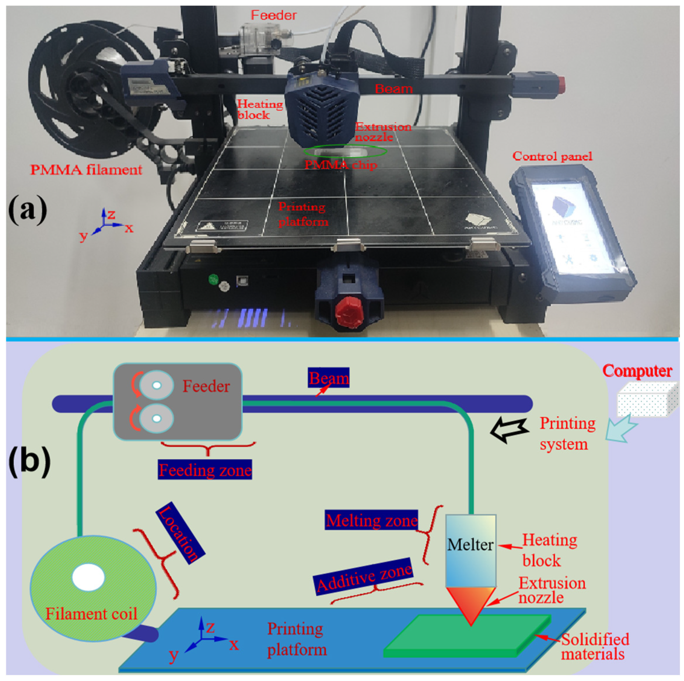
Figure 2.
The simulation diagram of temperature situation with 3D printing PMMA process.
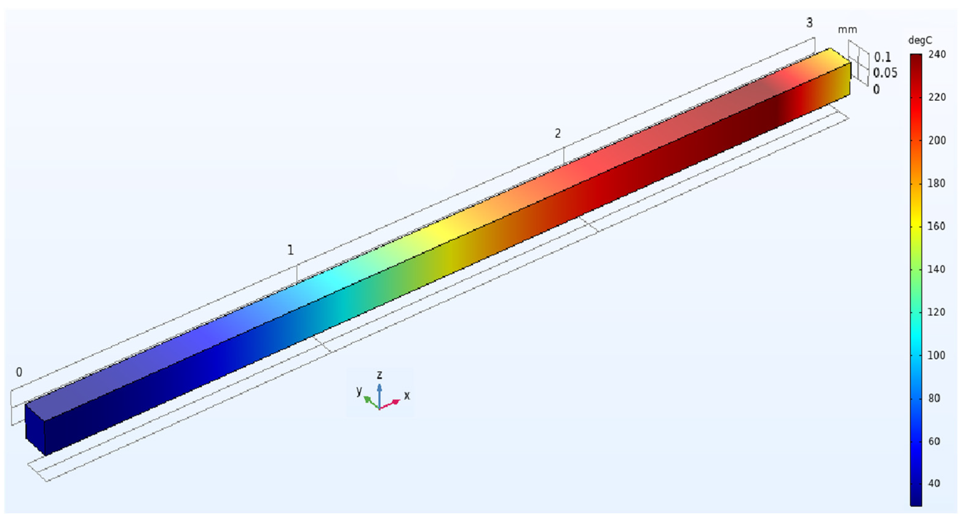
Figure 3.
The simulation diagram of thermal stress distribution with 3D printing PMMA process.
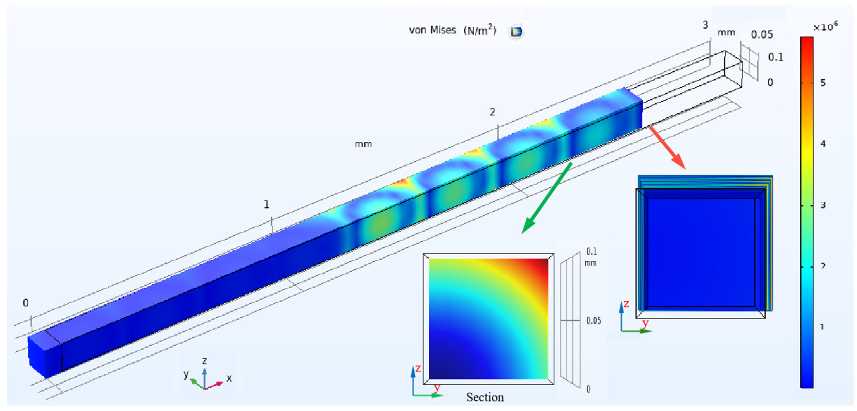
Figure 4.
The warping diagram material additive with FDM 3D printing PMMA process. (a)Priting material warping deformation with the numerical simulation system. (b)Priting material warping deformation with actual machining system. (c)The PMMA material warps with printing three layers along the vertical routein the Y-axis direction. (d) The morphology of optimized printing three layers PMMA materials.
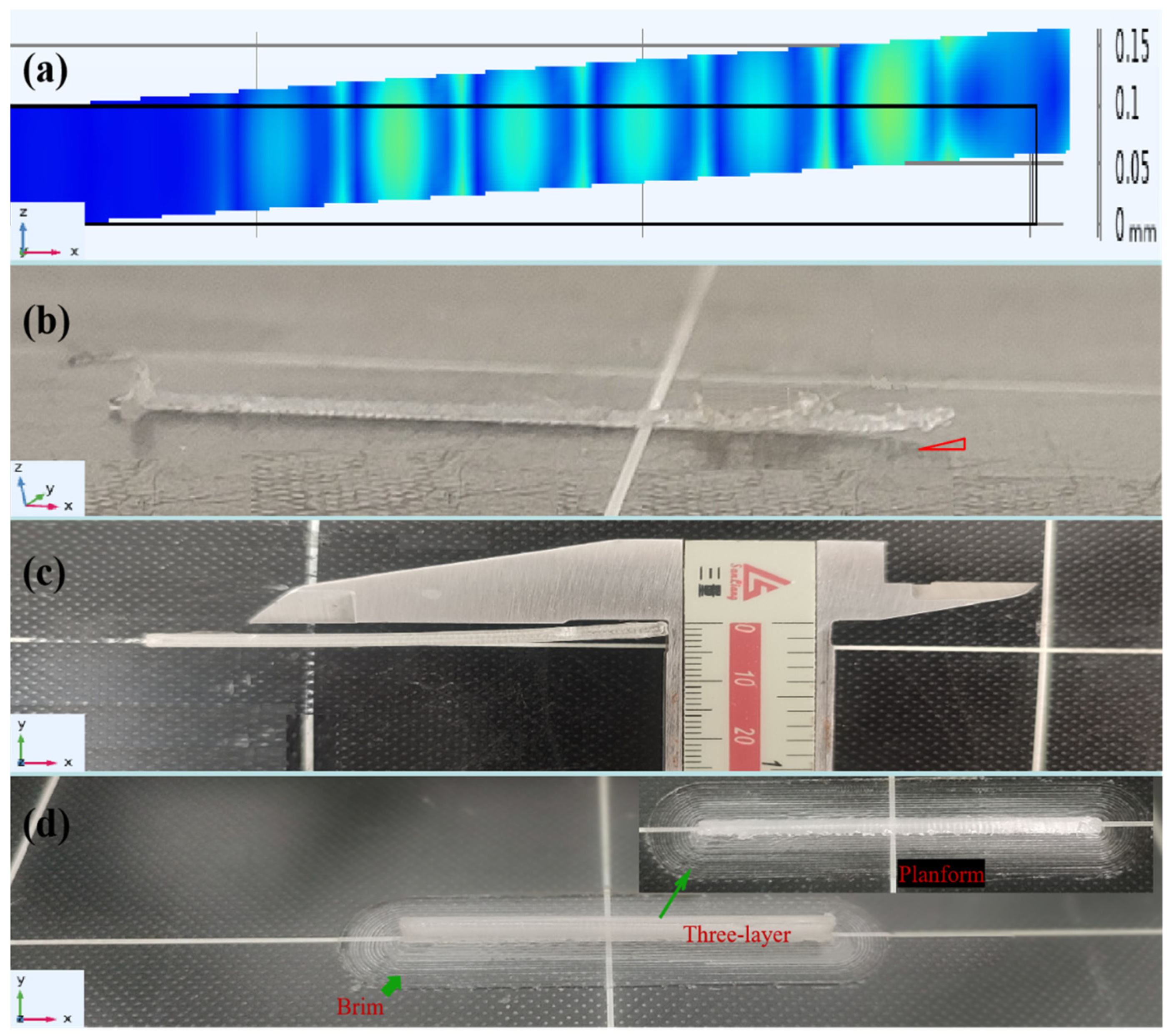
Figure 5.
The profile of microfluidic chip with single 3D printing capping technology. (a)The state of the chip sample without leakage. (b)The state of the chip sample with leakage. (c)The transparency tests of microfluidic chip sample surface.
Figure 5.
The profile of microfluidic chip with single 3D printing capping technology. (a)The state of the chip sample without leakage. (b)The state of the chip sample with leakage. (c)The transparency tests of microfluidic chip sample surface.
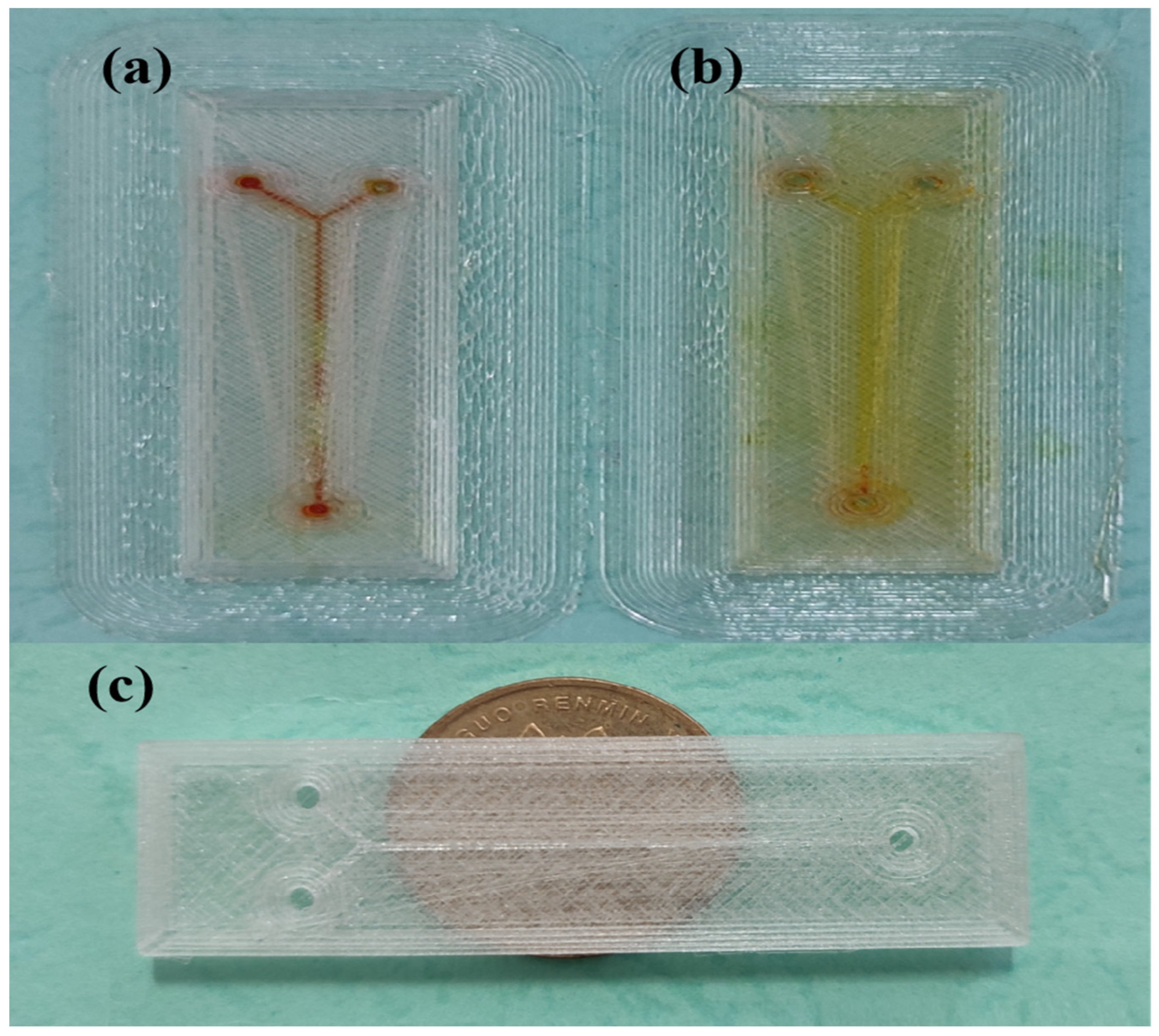
Figure 6.
The profile of microfludic chip with microchnnel of 200 μm. (a)The shape of channel cross-sections of 200 μm. (b)The microchnnel of 200 μm without leak and clog.
Figure 6.
The profile of microfludic chip with microchnnel of 200 μm. (a)The shape of channel cross-sections of 200 μm. (b)The microchnnel of 200 μm without leak and clog.
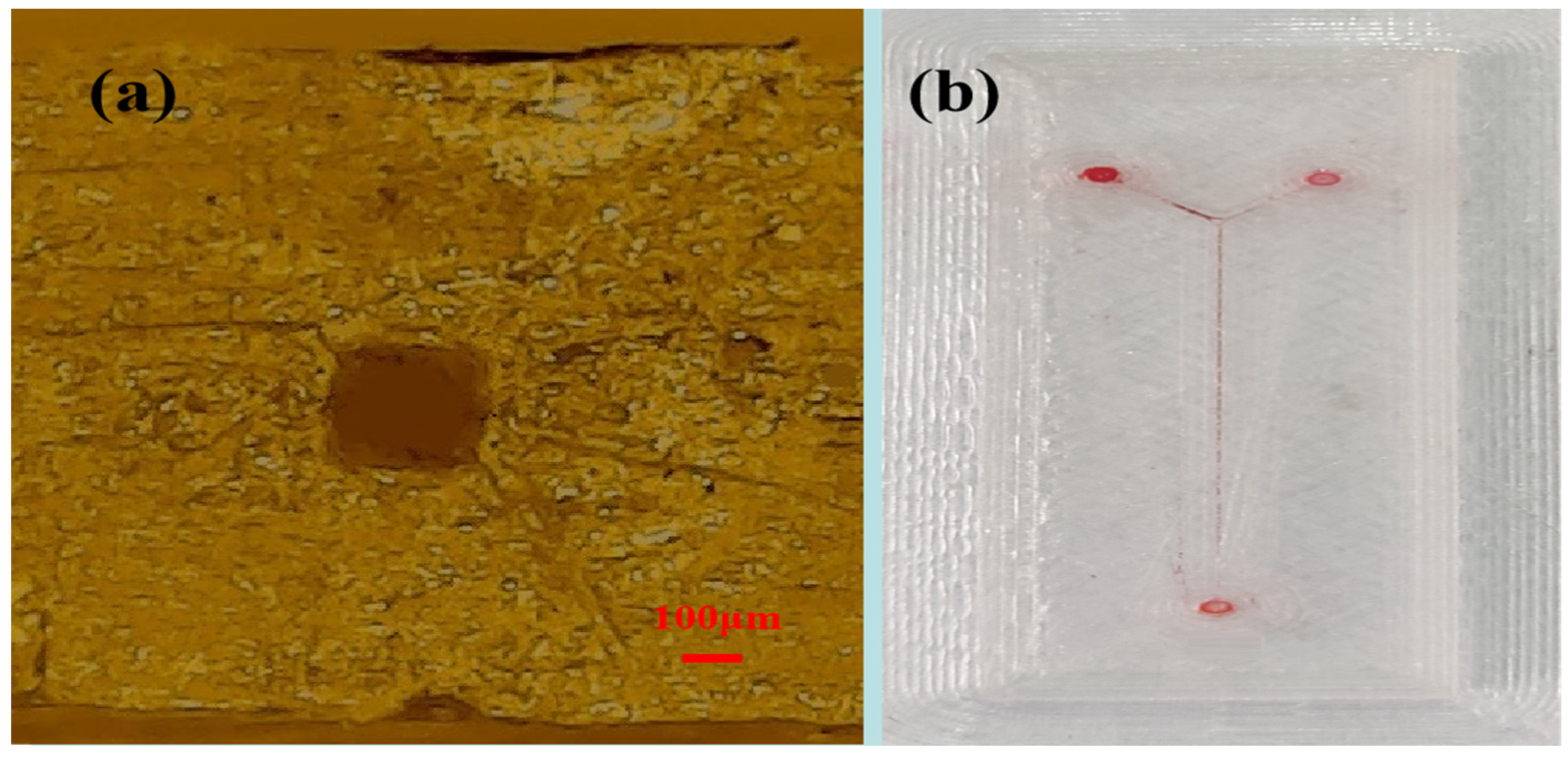
Figure 7.
The Roughness survey diagram of microchannel with FDM 3D printing process. (a)Roughness value. (b)Roughness ripple.
Figure 7.
The Roughness survey diagram of microchannel with FDM 3D printing process. (a)Roughness value. (b)Roughness ripple.
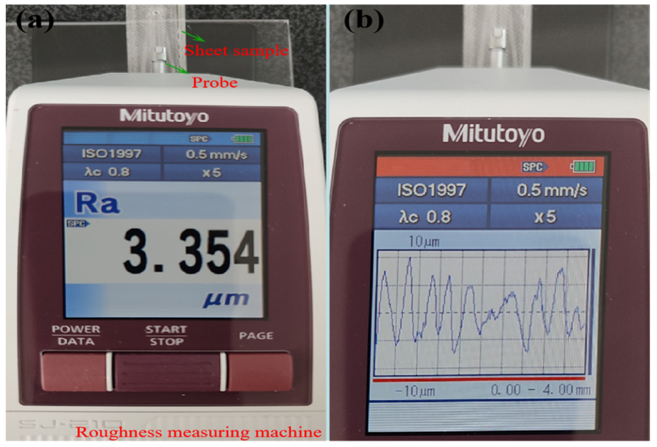
Figure 8.
A factor response figure.
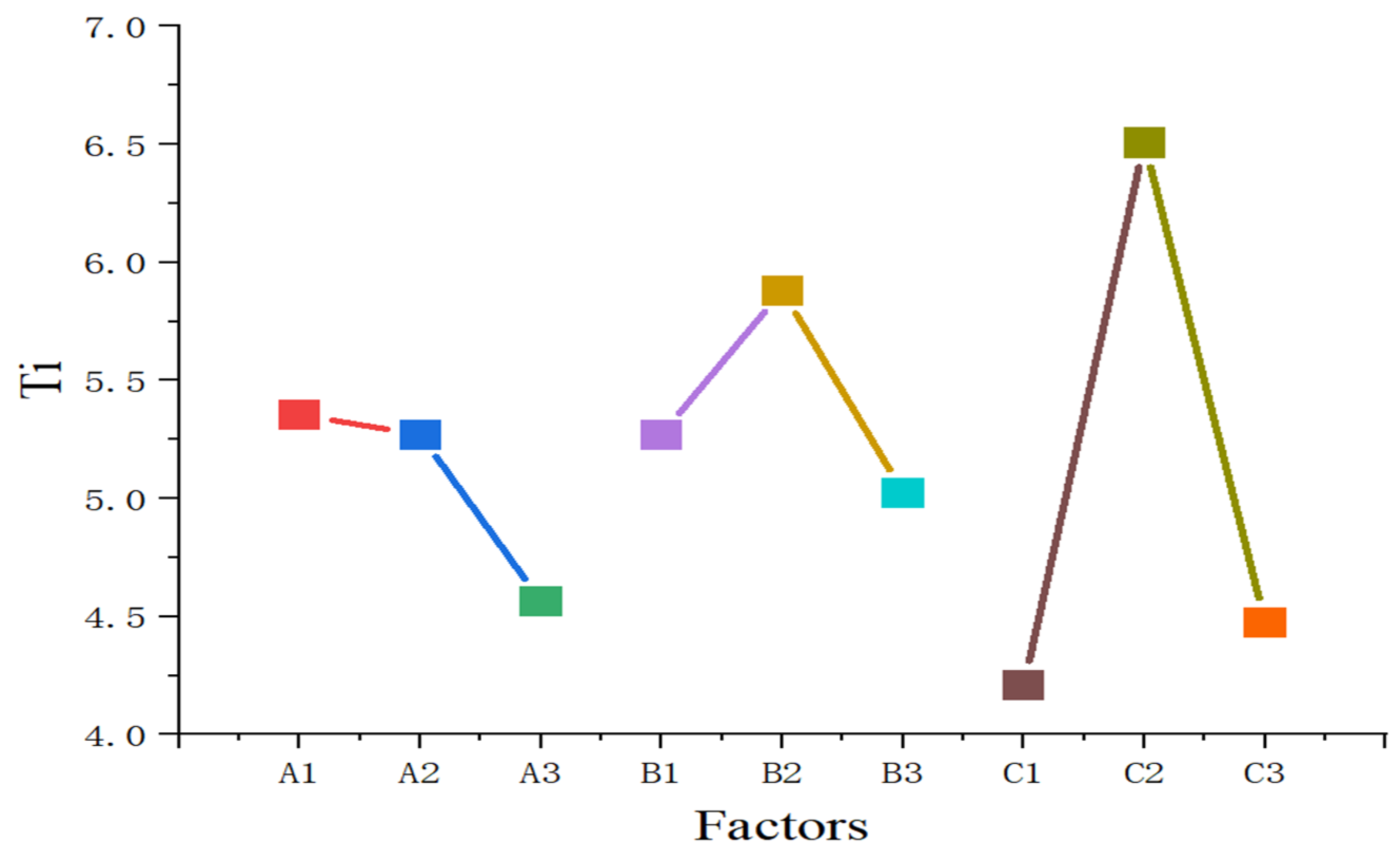
Figure 9.
The roughness of PMMA microchannel with optimized 3D printing parameters. (a)Roughness value. (b)Roughness ripple.
Figure 9.
The roughness of PMMA microchannel with optimized 3D printing parameters. (a)Roughness value. (b)Roughness ripple.
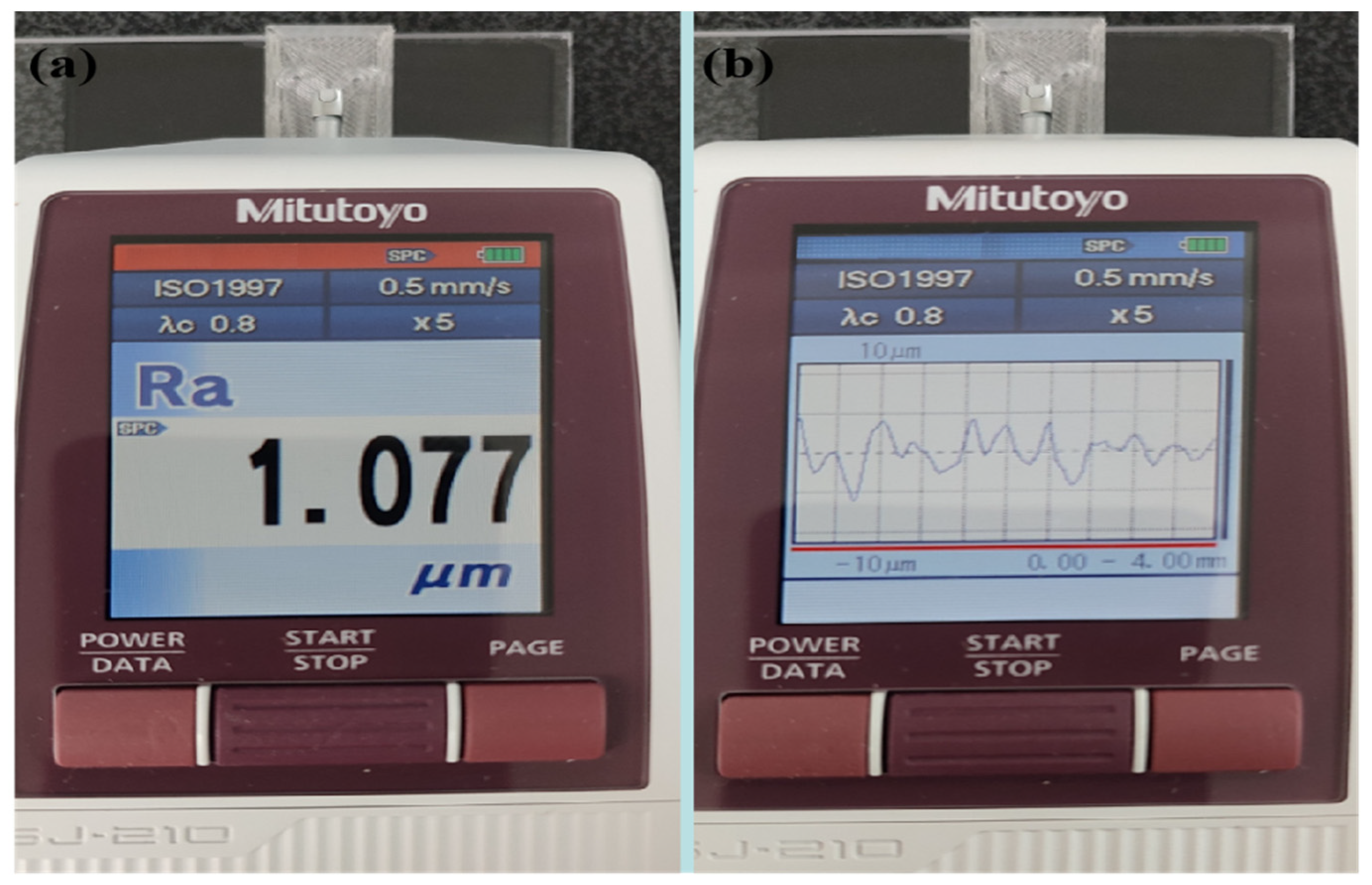
Figure 10.
The three dimensions structure diagrams of microreactor.
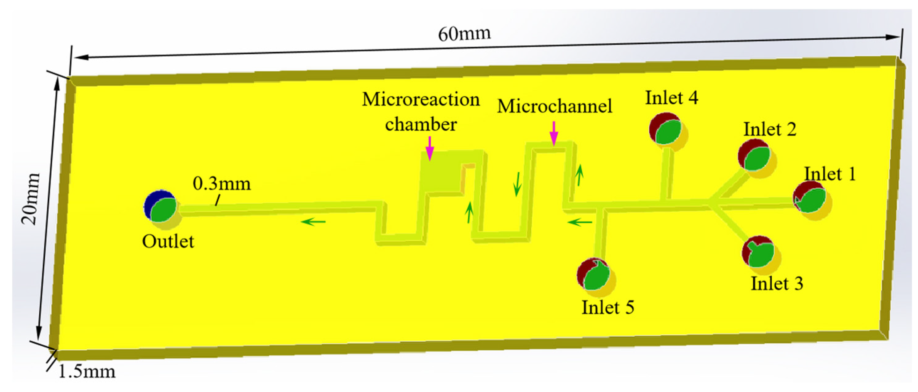
Figure 11.
Experimental diagram of chemical reaction with copper ion and ammonia water in microreactor.
Figure 11.
Experimental diagram of chemical reaction with copper ion and ammonia water in microreactor.
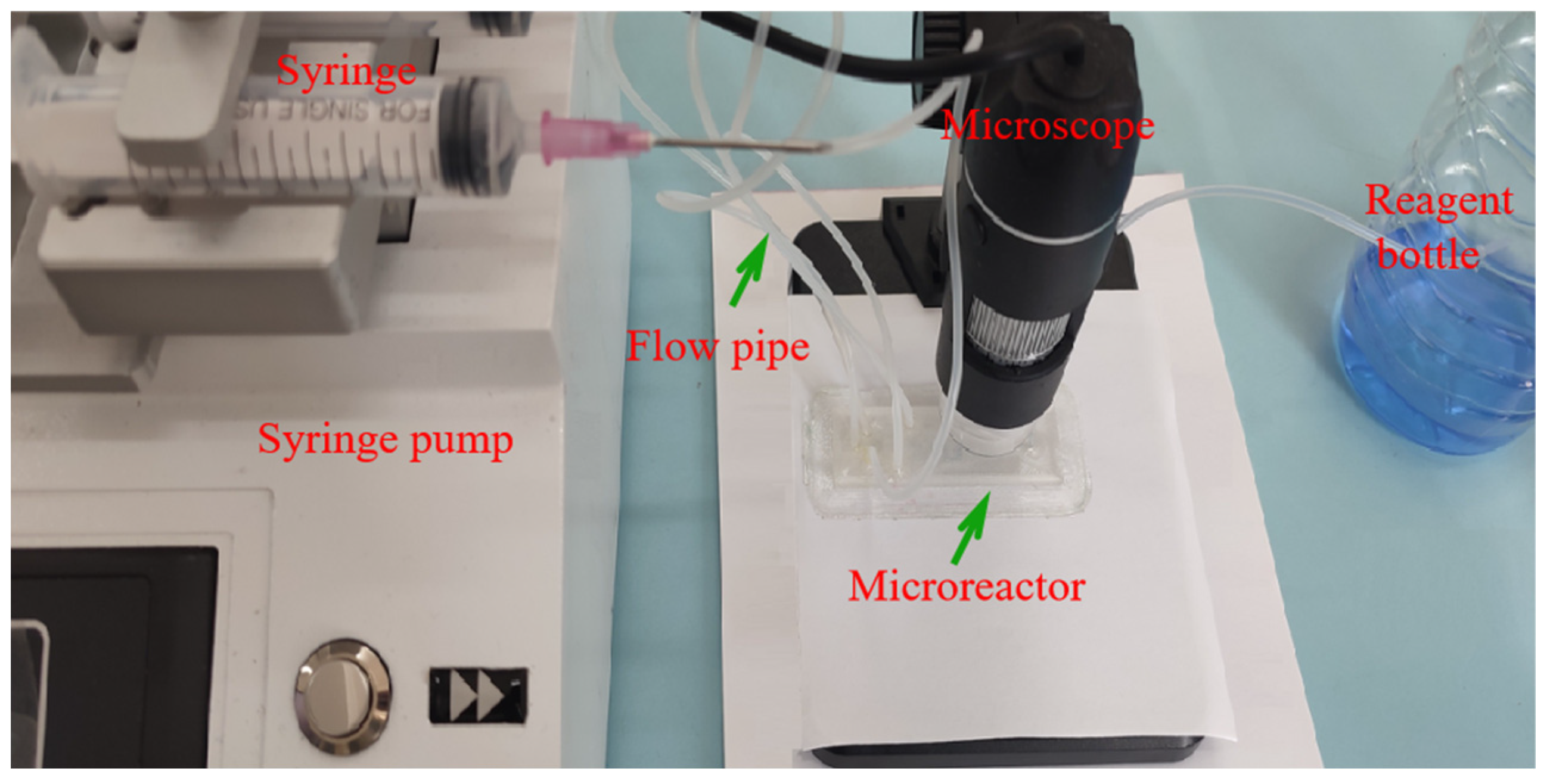
Figure 12.
Chemical reaction process of copper ion and ammonia water in microreactor. (a)Overall morphology of microreactor. (b)Local appearance at the output area. (c)Magnifying picture by microscope.
Figure 12.
Chemical reaction process of copper ion and ammonia water in microreactor. (a)Overall morphology of microreactor. (b)Local appearance at the output area. (c)Magnifying picture by microscope.
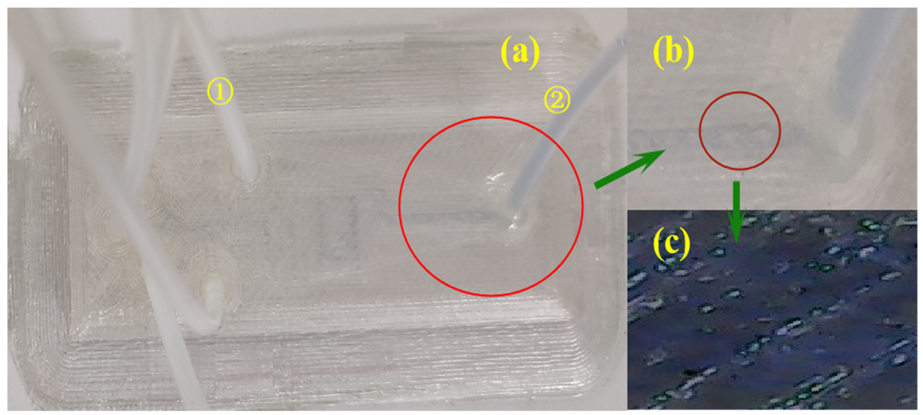
Figure 13.
The Copper hydroxide color diagram with different number copper ions.(a)One syringe containing copper ion. (b)Two syringes containing copper ion. (c)Three syringes containing copper ion. (d)Four syringes containing copper ion.
Figure 13.
The Copper hydroxide color diagram with different number copper ions.(a)One syringe containing copper ion. (b)Two syringes containing copper ion. (c)Three syringes containing copper ion. (d)Four syringes containing copper ion.
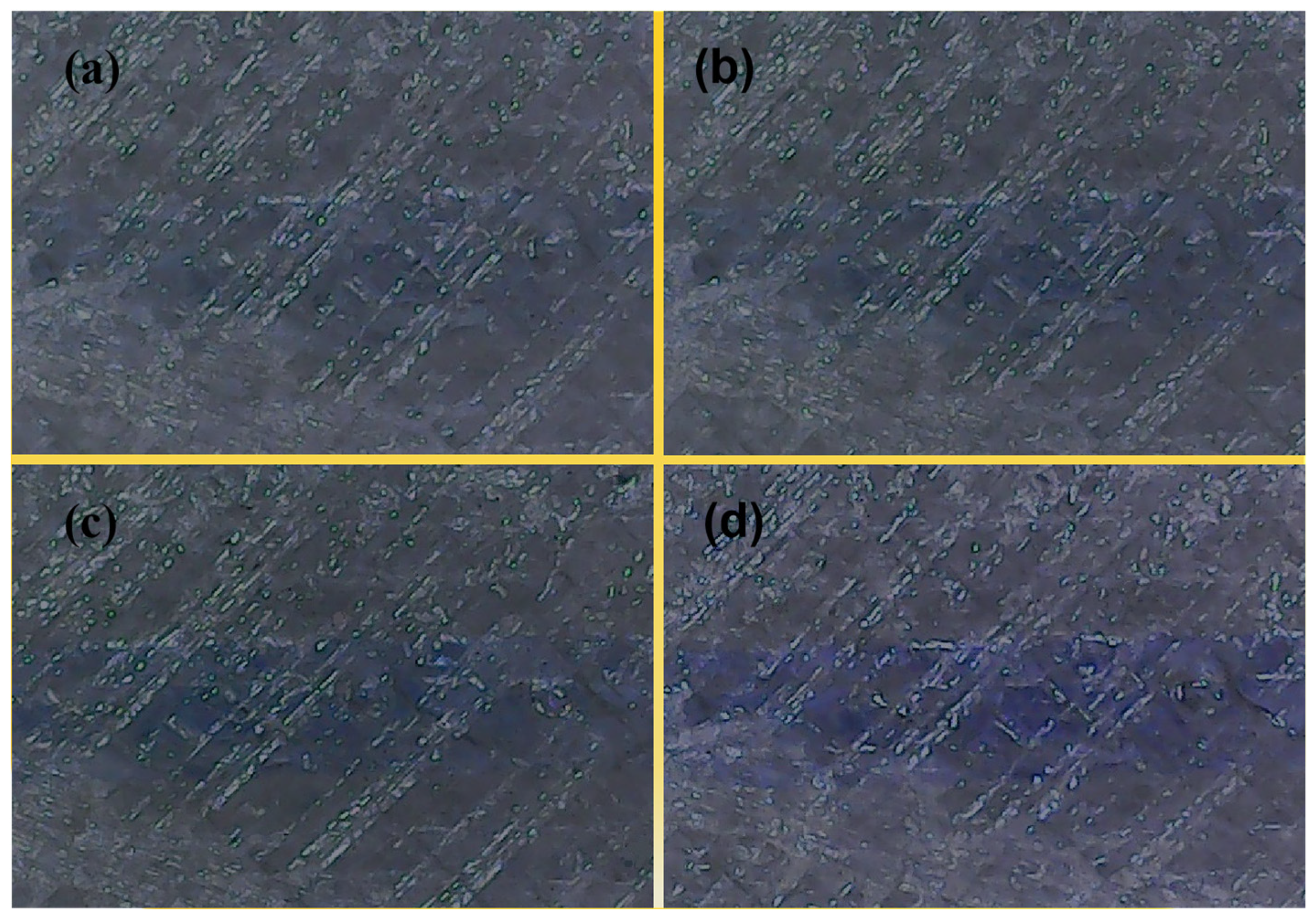
Figure 14.
Color data sheet for the number of different masses of copper ions.
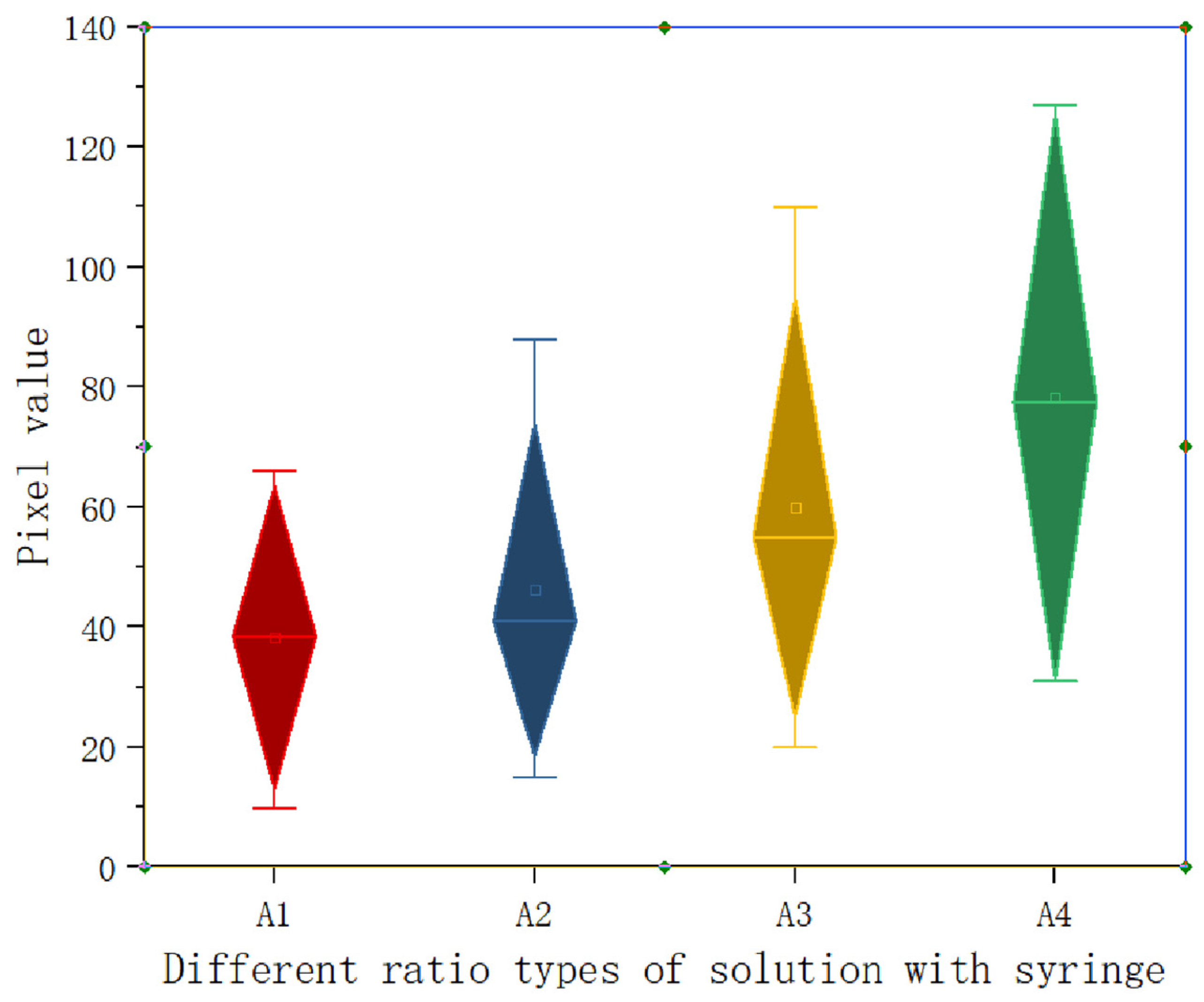

Table 1.
Orthogonal levels and factors.
| Levels | Factor | ||
|---|---|---|---|
| A (Nozzle temperature)(℃) | B (Printing speed)(mm/s) | C (Layer height) (mm) |
|
| 1 | 210 | 25 | 0.1 |
| 2 | 220 | 30 | 0.15 |
| 3 | 230 | 35 | 0.2 |
Table 2.
The corresponding parameters of experiment of each group.
| No. | A | B | C |
|---|---|---|---|
| 1 | 1 | 1 | 1 |
| 2 | 1 | 2 | 2 |
| 3 | 1 | 3 | 3 |
| 4 | 2 | 1 | 2 |
| 5 | 2 | 2 | 3 |
| 6 | 2 | 3 | 1 |
| 7 | 3 | 1 | 3 |
| 8 | 3 | 2 | 1 |
| 9 | 3 | 3 | 2 |
Table 3.
The factors response.
| No. | A | B | C | Average value H(μm) |
|---|---|---|---|---|
| 1 | 1 | 1 | 1 | 4.111 |
| 2 | 1 | 2 | 2 | 7.988 |
| 3 | 1 | 3 | 3 | 3.964 |
| 4 | 2 | 1 | 2 | 6.158 |
| 5 | 2 | 2 | 3 | 3.915 |
| 6 | 2 | 3 | 1 | 5.736 |
| 7 | 3 | 1 | 3 | 5.544 |
| 8 | 3 | 2 | 1 | 2.776 |
| 9 | 3 | 3 | 2 | 5.374 |
| T1 | 5.354 | 5.271 | 4.208 | |
| T2 | 5.270 | 5.880 | 6.507 | |
| T3 | 4.565 | 5.025 | 4.474 | |
| R | 0.79 | 0.85 | 2.30 |
Disclaimer/Publisher’s Note: The statements, opinions and data contained in all publications are solely those of the individual author(s) and contributor(s) and not of MDPI and/or the editor(s). MDPI and/or the editor(s) disclaim responsibility for any injury to people or property resulting from any ideas, methods, instructions or products referred to in the content. |
© 2025 by the authors. Licensee MDPI, Basel, Switzerland. This article is an open access article distributed under the terms and conditions of the Creative Commons Attribution (CC BY) license (http://creativecommons.org/licenses/by/4.0/).
Copyright: This open access article is published under a Creative Commons CC BY 4.0 license, which permit the free download, distribution, and reuse, provided that the author and preprint are cited in any reuse.


