Submitted:
05 February 2025
Posted:
07 February 2025
You are already at the latest version
Abstract
This paper presents a low-power CMOS receiver with complex continuous-time delta-sigma ADC designed for IoT applications in the 2.4 GHz band. The architecture employs a quadrature bandpass continuous-time delta-sigma ADC optimized for Bluetooth Low Energy (BLE) standards, achieving an ENOB of 10.9 bits while consuming only 0.81 mW from a 1.0V supply. The receiver demonstrates impressive performance metrics, including a sensitivity of -95 dBm at 10⁻³ bit error rate, an image rejection ratio of 54.2 dBc, and a spurious-free dynamic range of 79.8 dBc. Operating at a 1.5 MHz intermediate frequency with 2 MHz bandwidth, the ADC achieves superior energy efficiency with a figure of merit (FOMW) of 103.2 fJ/conv. Implemented in 28nm CMOS technology, the complete receiver occupies 0.375 mm² for the RF front-end and 0.145 mm² for the ADC while consuming 4.08 mW total power, making it well-suited for battery-powered IoT sensor nodes requiring both power efficiency and reliable wireless connectivity.
Keywords:
Bluetooth low energy (BLE)
; continuous-time delta-sigma ADC
; complex bandpass ADC
; CMOS
; Internet of Things (IoT)
; low-power receiver
; wireless sensor networks (WSN)
; low-IF architecture
; image rejection
; energy efficiency
1. Introduction
The Internet of Things (IoT) has emerged as a transformative paradigm, revolutionizing how we interact with our environment. As IoT devices grow exponentially, there is increasing demand for low-power, cost-effective wireless communication solutions [1,2]. This proliferation of interconnected smart devices necessitates innovative receiver designs that meet stringent IoT requirements while maintaining energy efficiency and compact form factors.
In IoT receiver design, the low-IF (Intermediate Frequency) architecture has gained traction by balancing power efficiency and performance. This architecture offers advantages over traditional direct conversion (zero-IF) receivers, including improved DC offset and flicker noise performance. However, low-IF faces image rejection challenges crucial for maintaining signal integrity amid interference. To address this, complex continuous-time sigma-delta analog-to-digital converters (ADCs) provide an effective solution. These ADCs perform both analog-to-digital conversion and image rejection, simplifying receiver architecture while maintaining high performance. Their continuous-time implementation provides inherent anti-aliasing filtering, reducing analog filtering requirements before the ADC stage.
The 2.4 GHz ISM (Industrial, Scientific, and Medical) band has become popular for IoT applications due to its global availability and support for protocols like Bluetooth Low Energy (BLE) [2] and Zigbee [3], as shown in Figure 1. These protocols suit short-range communication and offer low power consumption, making them ideal for battery-powered IoT devices.
IoT receiver design faces several critical challenges. Power consumption is paramount, as IoT devices must operate long-term on battery power or energy harvesting. This demands ultra-low power circuits and architectures that maintain performance while minimizing energy use. The evolving IoT ecosystem requires flexible receivers supporting multiple communication protocols, with adaptable modulation schemes and data rates at low power consumption.
Integration presents another challenge. Single-chip solutions must incorporate complex functionalities while reducing system cost and size for space-constrained IoT devices. This necessitates innovative circuit topologies and system architectures that achieve high integration without performance compromise. The analog-to-digital converter design significantly impacts overall receiver performance [5,6]. ADCs must handle wide dynamic ranges and maintain resolution across varied signal conditions while consuming minimal power. Continuous-time sigma-delta ADCs offer an effective balance between performance and power efficiency for these requirements [7].
This paper presents a low-power CMOS receiver for 2.4 GHz ISM band IoT applications, compatible with BLE protocol. The design combines low-IF architecture with a complex continuous-time sigma-delta ADC for efficient image rejection and high-performance analog-to-digital conversion. Our integrated approach creates a power-efficient, compact receiver meeting modern IoT requirements.
The design emphasizes minimal power consumption while maintaining BLE performance standards. The complex continuous-time sigma-delta ADC serves dual purposes: bandpass filtering for image rejection in low-IF receivers and simplified architecture for reduced power consumption and improved signal quality.
The following sections detail design considerations, circuit implementations, and performance analysis. We explore optimization techniques including adaptive biasing, efficient frequency synthesis, and innovative CMOS circuit topologies. This work advances IoT communication by addressing low-power design, image rejection, and protocol compatibility challenges. The architecture enables extended battery life, enhanced connectivity, and improved system performance for next-generation IoT devices.
2. A Comparative Analysis of IoT Receiver Architectures
Direct conversion and Low-IF represent the primary receiver architectures for BLE protocol IoT applications, as shown in Figure 2 [8]. Direct conversion receivers down-convert RF signals to baseband, offering simpler design and lower power consumption, but suffer from DC offset and flicker noise issues [9]. Low-IF receivers convert to a non-zero intermediate frequency, providing better immunity to these issues at the cost of higher power consumption and complexity [10].
For 2.4 GHz ISM band BLE applications, architecture choice significantly impacts system performance. Direct conversion receivers particularly struggle with I/Q mismatch and DC offset issues, affecting packet reception rates [11].
Low-IF receivers provide superior DC offset immunity through non-zero intermediate frequency processing - crucial for IoT applications where power constraints limit DC offset compensation [12]. This architecture inherently guards against flicker noise, essential for narrow-band BLE protocols with DC-concentrated baseband signals [13].
The low intermediate frequency processing enables effective channel filtering and adjacent channel rejection, improving selectivity in dense IoT deployments [10]. Low-IF better handles I/Q imbalance versus direct conversion, enhancing demodulation reliability for complex modulation schemes [14]. Additionally, the absence of DC offset simplifies automatic gain control implementation, improving dynamic range handling [15].
3. Optimizing ADC Dynamic Range for BLE Protocol: A Comprehensive Analysis
BLE receiver ADC specifications demand precise balancing to achieve optimal system performance. The ADC must deliver a dynamic range exceeding 60 dB to effectively process signals ranging from weak desired signals at -77 dBm to strong adjacent channel blockers at -50 dBm, as illustrated in Figure 3 [16].
The system incorporates essential margin requirements for reliable operation. A 10 dB back-off margin prevents the ADC's inherent noise floor from degrading receiver sensitivity, while an additional 6 dB margin accommodates the stepped transitions of automatic gain control (AGC) implementations. These combined margins ensure stable system operation across varying signal conditions. The ADC must maintain a minimum signal-to-noise ratio (SNR) of 9 dB even under maximum blocker conditions, translating to approximately 4-bit resolution when operating at sampling frequencies between 10-14 MHz. This specification balances quantization noise requirements with processing bandwidth constraints.
A signal-to-noise-and-distortion ratio (SNDR) target of 24 dB has proven sufficient for maintaining robust system performance. The ADC's performance integrates closely with the baseband filtering architecture, where digital complex bandpass filtering provides crucial antialiasing and image rejection functions. This filtering maintains a bit error rate (BER) of 0.1% or better by attenuating out-of-band blockers before they can saturate the ADC's input stage. Performance enhancement through oversampling techniques offers additional resolution improvements.
Implementation requirements demand that the ADC handle the complete range of signal conditions specified in the BLE standard [17]. The sampling frequency must be carefully selected to capture the required signal bandwidth while preventing interferer aliasing. These comprehensive specifications ensure effective BLE signal digitization with robust performance amid various interferers and blockers in the increasingly congested 2.4 GHz ISM band. The successful integration of resolution, sampling rate, and filtering requirements enables reliable wireless communication in this challenging environment.
4. Complex Continuous-Time Delta-sigma ADCs: Principles and Challenges
Complex bandpass continuous-time sigma-delta analog-to-digital converters (QB-CTΔΣADC) offer sophisticated bandpass signal digitization, as shown in Figure 4 [18]. These ADCs excel in software-defined radio and low-IF receiver applications by mitigating image problems without complex analog image-reject filters. The architecture uses a feedback-type quadrature bandpass continuous-time sigma-delta modulator (QB-CTΔΣM), implementing complex integrators through cross-coupled I/Q integrator pairs [19].
The feedback topology delivers key advantages in the signal transfer function (STF): superior filtering characteristics, enhanced anti-aliasing without gain peaking, and elimination of the feed-forward designs' summing stage before quantization [20]. This architecture effectively handles out-of-band blockers, which often exceed desired in-band signal strength in receiver applications [21].
The sigma-delta loop's complex signal processing implements optimized transfer functions through careful noise transfer function design and strategic complex notch placement at the signal band center frequency [22]. This results in doubled noise shaping capability over conventional real bandpass modulators.
Each QB-CTΣΔM stage comprises two cross-coupled low-pass CTΣΔM (LP-CTΣΔM) units. Figure 5 illustrates the block diagram of a single QB-CTΣΔM stage [23]. The single-loop LP-CTΣΔM filter transfer function HLP(jω) is expressed in equation (1) and depicted by the dotted line in Figure 5.
The single-loop QB-CTΣΔM transfer function HBP(jw) is derived by frequency shifting HLP(jω) to center frequency ωC, substituting s-jωC for s. This shifts the LP-CTΣΔM cutoff frequency ω0 to ωC ± ω0. Equation (2) describes the resulting HBP(jw), with Q representing the QB-CTΣΔM quality factor.
The implementation of an ADC with QB-CTΣΔMs presents several critical challenges that must be carefully addressed. Path mismatches between I/Q channels can significantly degrade image rejection performance, necessitating careful layout techniques and, potentially, calibration mechanisms [24]. Clock jitter sensitivity is another crucial concern, as timing errors in the feedback DAC directly impact conversion accuracy, requiring robust clock distribution networks and carefully designed DAC switching schemes [25]. The feedback topology, which must process both the input signal and noise, demands appropriate filter coefficient selection and circuit topology optimization to accommodate larger signal swings effectively. Stability considerations become particularly complex due to interactions between I/Q paths, requiring comprehensive stability analysis that accounts for variations in operating conditions [26]. Additionally, various non-idealities—such as I/Q mismatches, DAC element mismatching, and excess loop delay—often necessitate sophisticated calibration schemes [27].
Despite these challenges, the continuous-time implementation offers several advantages over discrete-time alternatives, including inherent anti-aliasing filtering, lower power consumption, higher potential sampling rates, and freedom from switched-capacitor settling constraints. These benefits make complex CT-ΣΔADCs particularly well-suited for modern wireless communication systems, especially in IoT applications, where power efficiency and performance must be carefully balanced.
4. Proposed Quadrature Bandpass Continuous-Time Delta-sigma ADC
4.1. Quadrature Bandpass Continuous-Time Delta-sigma ADC Architecture
The proposed receiver architecture incorporates a quadrature bandpass continuous-time delta-sigma analog-to-digital converter (CT-ΣΔ ADC) specifically designed to meet BLE specifications, as shown in Figure 4. The ADC implementation features carefully selected performance parameters that align with the requirements of modern wireless communication systems, with a particular focus on BLE applications. Within its operational specifications, the ADC demonstrates a robust in-band dynamic range, which is crucial for reliable wireless communication.
The system processes signals within an integrated bandwidth of 2 MHz, operating in the frequency range of 0.5 MHz to 2.5 MHz. This range is strategically chosen to optimize receiver performance while maintaining compatibility with BLE signal requirements.
In terms of signal handling, the ADC achieves a dynamic range of 60 dB, enabling it to process both strong and weak signals effectively. This specification ensures the receiver can accommodate the wide variation in signal strengths typically encountered in BLE applications, from nearby devices to those at the maximum specified range.
The architecture's continuous-time implementation provides inherent antialiasing capabilities, achieving over 39 dB attenuation at the first sampling zone. This built-in antialiasing functionality is a significant advantage of the continuous-time approach, effectively suppressing unwanted high-frequency components that could otherwise interfere with the desired signal.
Furthermore, the system exhibits strong image rejection capabilities, with an image rejection ratio specified to be better than -32 dBc. This specification ensures that the receiver can effectively suppress signals at the image frequency, which is crucial for maintaining signal quality and preventing interference in the quadrature receiver architecture.
These comprehensive specifications demonstrate that the ADC design meets the necessary performance metrics to support reliable BLE communication while maintaining practical implementation considerations. The combination of bandwidth, dynamic range, antialiasing, and image rejection capabilities makes this architecture particularly well-suited for modern wireless communication applications, especially within the context of BLE systems.
4.2. Quadrature Bandpass Continuous-Time Delta-sigma ADC Circuit Design
4.2.1. 4-bit Feedback Current Digital-to-Analog Converter Circuit
4-bit feedback digital-to-analog converters (FBDACs) are circuits that implement the negative feedback factors a₁, a₂, a₃, and g₁ of the QBP-CTΣΔM, as shown in Figure 4. It employs the bipolar topology depicted in Figure 5(a) rather than the unipolar approach shown in Figure 5(b), which allows the DAC current to be reduced by half compared to the unipolar version. To improve the output impedance of the DAC unit cell, cascode transistors are used in the current source, utilizing both NMOS and PMOS configurations. In the current design, the unit current of the bipolar topology is specifically designed to be half that of the unipolar topology. This design choice serves two purposes: reducing noise contribution and lowering current consumption in the bipolar topology. Additionally, it enables smaller capacitor loads, resulting in a more compact overall design.
The linearity of the DAC is critical for the QBP-CTΣΔM to achieve the required signal-to-noise ratio (SNR). To address DAC linearity issues, a data-weighted averaging (DWA) technique is implemented, effectively mitigating these concerns without requiring large device areas for intrinsic device size matching. The DWA system operates by updating the pointer location in each cycle based on the current position and incoming data, as shown in Figure 5(c). Notably, the pointer-shifting logic for the DWA is kept separate from the main feedback path, ensuring that the pointer for the current data is immediately available without introducing additional logic delays. As a result, the only delay in the system comes from data propagation through the matrix.
The feedback DAC's final injection occurs at 0.5T after the quantizer's sampling edge. This timing allows sufficient time for SAR ADC subtraction, conversion, and DWA data transmission. Performance testing using 20 Monte Carlo post-simulations demonstrated impressive results, achieving a spurious-free dynamic range (SFDR) greater than 80 dB and a Signal-to-Quantization-Noise Ratio (SQNR) exceeding 67 dB.
IQ mismatch is an important design consideration due to the image rejection ratio (IRR) requirements. Monte Carlo simulations with 20 runs demonstrated that the current design achieves a worst-case IRR of approximately 60 dBc, which is sufficient to render the ADC's contribution negligible.
Figure 5.
(a) Unipolar and (b) bipolar current DAC cells and (c) 4-bit DWA pointer rotation.
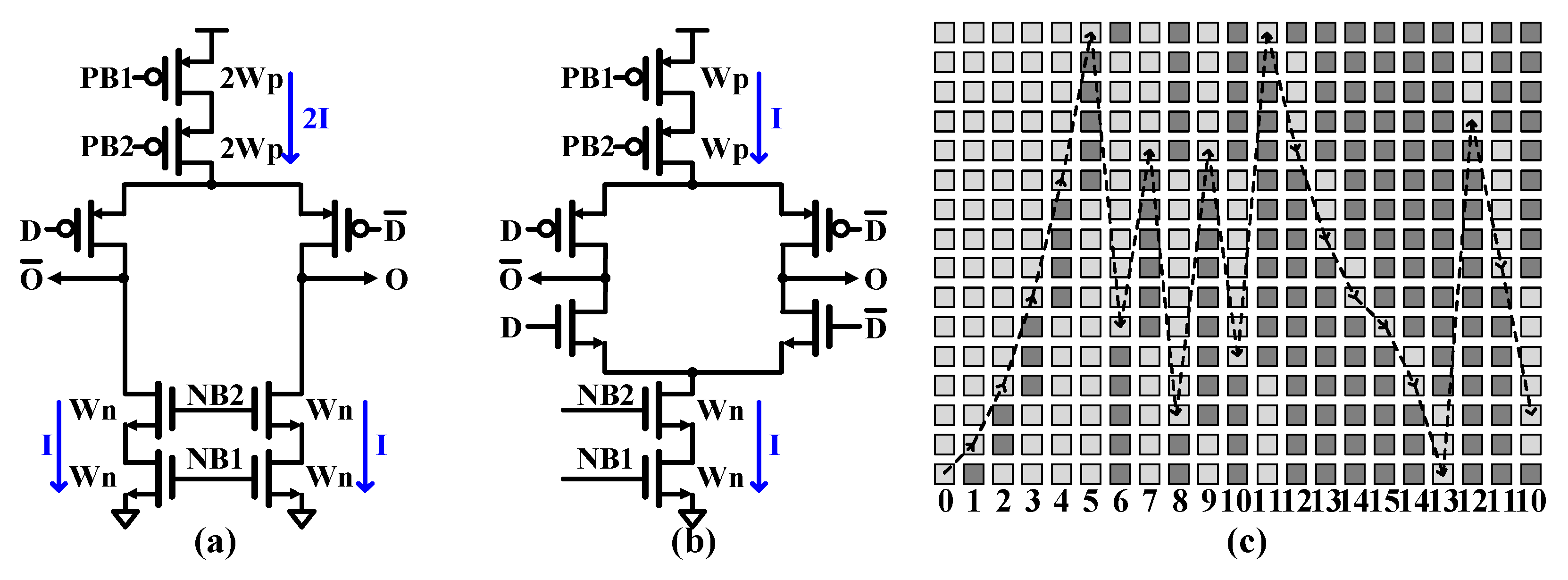
Figure 6.
FBDAC bias circuit.
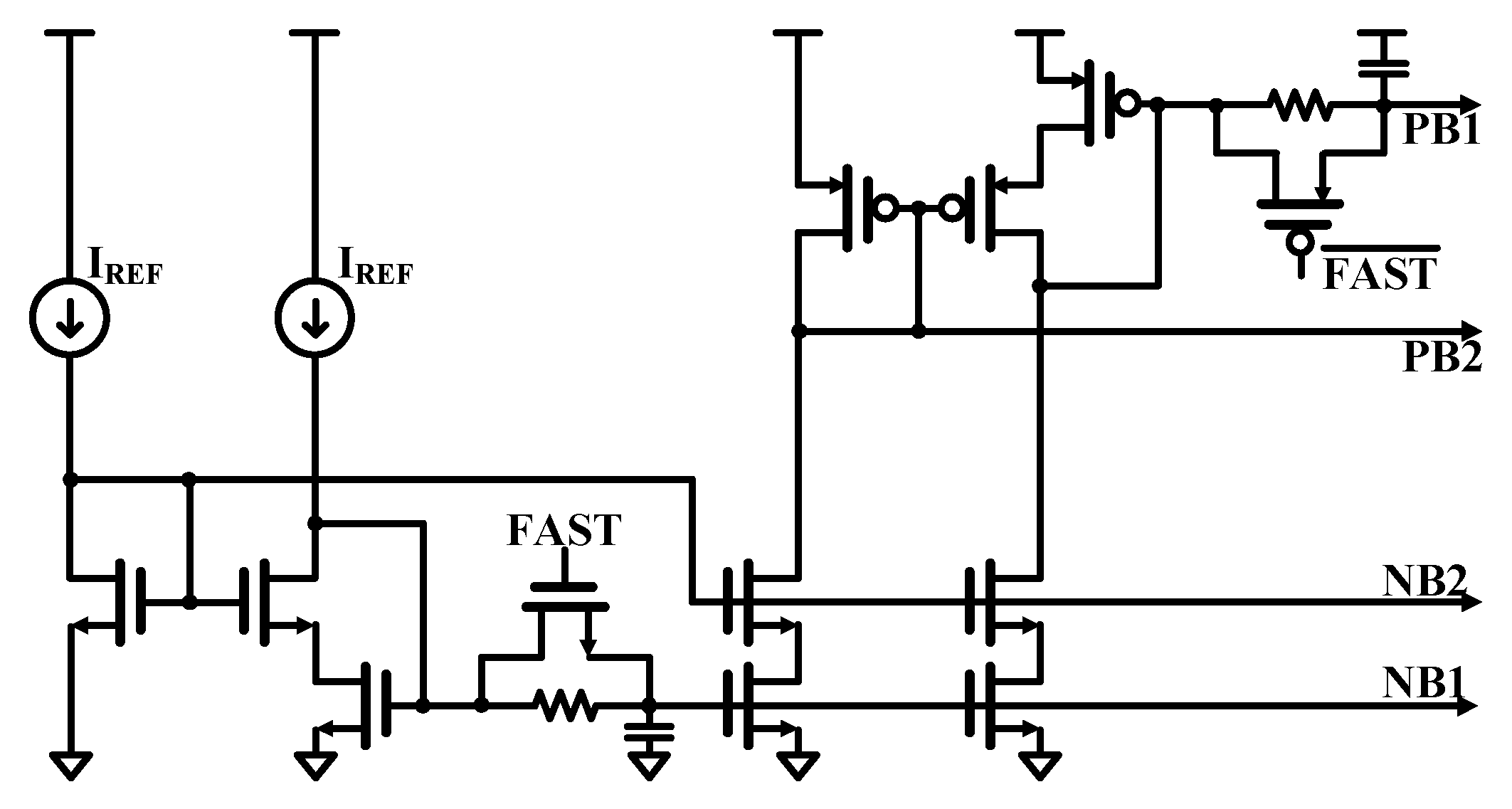
In the bias circuit design, the system operates with a 1 V supply voltage provided by an internal regulator (LDO), supporting a mismatch range of approximately ±10%, from 0.9 V to 1.1 V. Due to limited voltage headroom, source degeneration resistors are excluded from the design. The circuit benefits from reduced flicker noise sensitivity in the low-IF topology and a wider signal bandwidth. To meet the > 60 dB dynamic range requirement, the design increases the device length and reduces the device width, which decreases transconductance (gm) and increases saturation voltage (VDSAT).
The bias circuit incorporates an RC filter with a -3 dB corner bandwidth of approximately 48 kHz to suppress noise from the bandgap and bias generator circuits. To mitigate potential long settlement times caused by the RC filter, the design includes a fast-settle shorting switch activated by a loop filter reset signal. This approach achieves a settlement time of less than 30 μs, including the bandgap, bias generator, and loop filter reset timing, meeting the BLE system specification of 90 μs.
4.2.2. Active RC Integrator
Continuous-time loop filters can be implemented using either active-RC or Gm-C integrators, as shown in Figure 7 (a) and (b), each with distinct characteristics and trade-offs. For the proposed QBP-CTΣΔM, active-RC integrators are the preferred implementation approach, as they deliver enhanced linearity at comparable power consumption levels and can handle larger signal swings compared to Gm-C integrators. Additionally, operational transconductance amplifiers (OTAs) create more stable virtual grounds through closed-loop operation, independent of input conditions. While Gm-C integrators excel in terms of power efficiency and can achieve higher operational speeds, active-RC integrators are the more suitable choice for high-speed CTDSM due to their higher maximum stable input amplitude.
A two-stage amplifier can provide a higher overall gain compared to a single-stage amplifier. This is crucial for active-RC integrators, as it enhances accuracy and linearity in the integration process. However, two-stage amplifiers often employ Miller compensation to stabilize the circuit and prevent oscillations. Miller compensation typically requires a larger compensation capacitor, leading to increased power consumption because more power is needed to charge and discharge the larger capacitor.
To address this, a fully differential OTA without Miller compensation is employed in this work, as shown in Figure 7(c). The OTA utilizes conventional differential difference amplifier (DDA)-based common-mode feedback (CMFB). The implementation incorporates a combination of capacitive boosting (CB) and resistive boosting (RB) in the first stage, effectively increasing the pole frequency without relying on traditional Miller compensation. This approach mitigates typical limitations associated with Miller compensation, such as right-half-plane zeros and bandwidth constraints. Moreover, the input signals are uniquely connected to the second stage through AC coupling capacitors (CAC). This configuration enables higher gain by bypassing the first stage's gain limitations. Additionally, the cross-coupled structure in the second stage further enhances the overall gain of the amplifier. It achieves a unity-gain bandwidth of 200 MHz and a noise level of <30 nV/√Hz while consuming 70 µW.
RC calibration of the active-RC integrator plays a crucial role in the QBP-CTΣΔM, as it determines the frequency characteristics of the overall signal through resistance and capacitance values. These values are significantly affected by process, voltage, and temperature (PVT) variations. To compensate for these variations, the system implements an active-RC oscillator with a frequency of fOSC using resistors, capacitors, and OTAs with a simple switching configuration. The calibration process utilizes an external reference frequency of 32 MHz (fREF) that is relatively constant under PVT variations. The system counts how many times the reference clock (N) resonates while the internal oscillator resonates K times, as shown in equation (3).
where the N must result in a value of 1 or greater to accurately detect changes in capacitor 1 LSB value that corresponds to 2 % capacitive variation, which represents as equation (4).
The capacitor bank requires both a wide range and fine LSB resolution to accommodate all corner cases. The required capacitance range is from 1.1 pF to 4.4 pF. Using 1.1 pF as the basic unit and 25 fF as the LSB, the capacitance can be adjusted from 732 fF to 1.766 pF. The capacitor bank implements 5-bit controls to cover all PVT conditions, including resistance variations. The resistor is fixed at 32 kΩ, and the RC product is set to approximately the resolution of 2%, assuming an acceptable error margin of ±1%. Since frequency is inversely proportional to capacitance, achieving full linear coverage across the entire range is challenging. However, the capacitor was carefully adjusted to maximize linearity while maintaining a resolution of about 2% in the central region. A capacitor bank with 5-bit control was implemented to accommodate all PVT conditions, including variations in resistance.
RC calibration is performed using the successive approximation register (SAR) method with an fOSC of 2 MHz. After the predefined settling time of the active-RC oscillator, considering PVT variations, the number of reference clock cycles (N) is counted over four cycles (K=4) of the active-RC oscillator to achieve an accuracy of ±1% in the ideal case. Subsequently, N is compared with the predefined reference value of 128. The counter reset is synchronized with each clock cycle for precise counting. After verifying the final bit, the system generates an end-of-conversion signal, and the values are stored in eFuse as serial peripheral interface (SPI) values for future RC calibrations. The calibration demonstrates frequency convergence to 2 MHz across all PVT corners, with accuracy ranging between 98.9% and 104% of the target frequency. The capacitor codes vary across different corners and temperatures, ranging from 31/30 at the lowest corner to 1/0 at the highest corner, consistently maintaining the target frequency within the specified accuracy range.
4.2.3. 4-bit Quantizer
A delta modulator quantizes the difference between the current input data and the previous output data with a specific feedback gain, which is accomplished by a successive approximation register (SAR) ADC-type delta modulator through analog subtraction during the sampling phase. Conventional SAR ADC-type modulators are limited to unity feedback gain, as they share reference voltages between the sampling and conversion phases. Implementing non-unity feedback traditionally requires additional voltage references, which increases circuit complexity, area requirements, and static power consumption.
The proposed delta modulator provides non-unity feedback gain through an additional capacitive digital-to-analog converter (CDAC). This is achieved by modifying the ratio of two CDACs used in the sampling and conversion phases. When the feedback gain (α) is less than unity, the CDAC used in the sampling phase is smaller than the one used in the conversion phase, as shown in Figure 8(a). The value of α is calculated using Equation (5).
When the α is greater than unity, conversely, the sampling phase CDAC is larger than the conversion phase CDAC, as shown in Figure 8(b), and α is calculated as shown in Equation (6).
The VREFP should be α times larger than that of a conventional SAR ADC-type delta modulator to maintain the same quantization step size. The proposed structure achieves various feedback gains using an additional CDAC and an adjustable voltage reference generator.
Figure 9(a) shows the capacitor array layout with a thermometer-coded design, where each unit capacitor has a value of 250 aF, and eight identical unit capacitors are arranged in each row to form a 2 fF segment. Unlike binary weighting, this thermometer structure ensures monotonicity by using identical unit elements that are equally sized and switched sequentially. All top plates are connected together as a common node, while the bottom plates are individually connected to reference voltage switches, allowing for thermometer-code switching patterns. The layout employs a common-centroid technique with regular, repeated patterns to ensure optimal matching between unit capacitors and minimize manufacturing variations, as shown in the detailed zoom-in view of the unit capacitor structure.
The StrongARM comparator, as shown in Figure 9(b), is a clocked dynamic comparator that operates in two distinct phases: the reset phase and the evaluation phase. During the reset phase, when the clock is low, all internal nodes are precharged to VDD through reset transistors. This process ensures known initial conditions and minimizes memory effects. When the clock transitions to a high state, the evaluation phase begins as the tail current transistor activates and the reset transistors turn off. This allows the differential input pair to create an initial voltage imbalance at the internal nodes. This imbalance is then amplified by cross-coupled PMOS and NMOS pairs through positive feedback, which drives the outputs rapidly to opposite rails based on the input voltage difference. The StrongARM comparator achieves high speed and energy efficiency due to this regenerative positive feedback mechanism. This characteristic makes it particularly suitable for high-speed ADC applications where fast decision-making is crucial. The design of the comparator requires careful consideration of transistor sizing and layout symmetry to minimize offset and ensure reliable operation across variations in process, voltage, and temperature.
The 4-bit SAR logic performs analog-to-digital conversion using a binary search algorithm. After receiving a start signal, it samples the input voltage and holds it constant. The conversion begins with the most significant bit (B3), setting it to 1 and comparing the input voltage with the DAC output. Based on this comparison, B3 is either kept or cleared. The process continues similarly for B2, B1, and B0. After each bit decision, the system waits for the DAC to settle and the comparator to resolve. Once all four bits are determined, the system asserts an end-of-conversion signal, completing the process in five clock cycles: one for sampling and four for bit decisions. The final 4-bit value represents the digital approximation of the input analog voltage.
5. Experimental Results
The proposed receiver was fabricated in a 28nm CMOS process, as shown in Figure 10(a). The chip layout features an RF front-end area of 0.375 mm² and a QBP-CTΣΔM ADC area of 0.145 mm². In BLE mode operation, the receiver achieves a sensitivity of -95 dBm at 10⁻³ bit error rate while consuming 4.08 mW from a 1.0V supply. The QBP-CTΣΔM ADC portion draws 0.81 mW, which includes power consumption from the bias circuit for current distribution to active blocks, input/output drivers, and clock distribution circuitry.
Signal-to-noise ratio (SNR) measurements were conducted using a peak low-IF signal at 1.5 MHz with 100 Hz resolution, as illustrated in Figure 11. The feedforward architecture results in minimal harmonic distortion at the output. The design achieves a peak spurious-free dynamic range (SFDR) of 79.8 dBc, with an impressive image rejection ratio of 54.2 dBc during measurements.
The measured signal-to-noise-distortion ratio (SNDR) and signal-to-noise ratio (SNR) across different input signal levels are plotted in Figure 12. The ADC demonstrates peak performance with an SNDR of 67.5 dB at -2 dB relative to full scale (dBFS) and a peak SNR of 68.9 dB at -1 dBFS. For reference, the full-scale signal (0 dBFS) corresponds to a differential peak-to-peak voltage (VP-P) of 1V. The ADC achieves a dynamic range of 70.3 dB across its 2-MHz signal bandwidth (BW).
Intermodulation testing was performed to characterize the QBP-CTΣΔM ADC's linearity. When presented with two strong input signals at -15 dBFS at frequencies of 1.3 GHz and 1.7 GHz, the resultant intermodulation products measure 58.7 dBc below the fundamental tones, as shown in Figure 13.
Table 1 presents a performance comparison between the proposed receiver with CT-ΣΔM ADC and previously reported IoT receivers. Our design implements a low-IF architecture for BLE standards with an intermediate frequency (IF) of 1.5 MHz. The CT-QΣΔM ADC achieves an effective number of bits (ENOB) of 10.9, operates at a sampling frequency of 32 MHz, and provides a bandwidth (BW) of 2 MHz. To enable fair comparison, we evaluate the ADC performance using two established figures of merit: FOMS (equation 7 [28]) and FOMW (equation 8 [29]):
where ENOB = (SNDR(dB)-1.76)/6.02. The FOMS metric emphasizes resolution and dynamic range improvements, with higher values indicating better performance. Conversely, FOMW focuses on energy efficiency, where lower values represent better performance. The proposed CT-QBP ΔΣM ADC achieves a FOMS of 164.3 dB. While this figure is lower than some IoT sensor applications [30,31,32] due to our higher intermediate frequencies, our design demonstrates superior energy efficiency with the best FOMW among state-of-the-art implementations [30,31,32,33,34].
6. Conclusions
This paper presented a low-power CMOS receiver with a complex continuous-time delta-sigma ADC optimized for IoT applications in the 2.4 GHz band. The proposed design incorporates a quadrature bandpass continuous-time delta-sigma ADC that achieves an ENOB of 10.9 bits while consuming only 0.81 mW from a 1.0V supply. The ADC successfully provides a bandwidth of 2 MHz while operating at a 32 MHz sampling frequency, making it ideally suited for BLE applications.
The receiver architecture demonstrates several significant performance achievements through its innovative features. The carefully optimized low-IF architecture operating at 1.5 MHz IF frequency delivers strong image rejection capability with a measured IRR of 54.2 dBc. The design also achieves an excellent SFDR of 79.8 dBc, demonstrating its robust signal handling capabilities. Most notably, the architecture achieves superior energy efficiency with a FOMW of 103.2 fJ/conv, representing the best figure among current state-of-the-art implementations.
The complete receiver system demonstrates impressive sensitivity of -95 dBm at 10⁻³ bit error rate while maintaining low power consumption of 4.08 mW, with the ADC portion requiring only 0.81 mW. The design implementation in 28nm CMOS technology achieves a compact form factor, occupying just 0.375 mm² for the RF front-end and 0.145 mm² for the ADC. These specifications demonstrate that the proposed architecture successfully addresses the demanding requirements of modern IoT applications, particularly for BLE standards, by delivering an optimal balance between power efficiency, performance, and integration density.
The achieved specifications make this design particularly well-suited for battery-powered IoT sensor nodes where both power efficiency and reliable wireless connectivity are critical requirements. Future research directions could focus on further enhancing energy efficiency through adaptive biasing techniques and exploring additional power optimization strategies to extend battery life in IoT applications. The demonstrated architecture provides a robust foundation for advancing the development of next-generation low-power wireless sensor networks.
Funding
This research was supported in part by the Institute of Information & communications Technology Planning & Evaluation (IITP) grant funded by MSIT of Korea government under grant number RS-2023-00229689; in part by the National Research Foundation of Korea (NRF) funded by the Ministry of Science and Information and Communications Technology (MSIT) of Korean Government under grant number RS-2024-00445552. The EDA tool was supported by the Integrated Circuit Design Education Center (IDEC), Korea.
Institutional Review Board Statement
Not applicable.
Informed Consent Statement
Not applicable.
Data Availability Statement
Data are contained within the article.
Conflicts of Interest
The authors declare no conflicts of interest. The funders had no role in the design of the study; in the collection, analyses, or interpretation of data; in the writing of the manuscript; or in the decision to publish the results.
References
- Zhang, Y.; Zhang, F.; Shakhsheer, Y.; Silver, J.D.; Klinefelter, A.; Nagaraju, M.; Boley, J.; Pandey, J.; Shrivastava, A.; Carlson, E.J.; et al. A Batteryless 19 μW MICS/ISM-Band Energy Harvesting Body Sensor Node SoC for ExG Applications. IEEE J. Solid-State Circuits 2013, 48, 199–213. [Google Scholar] [CrossRef]
- Cavliwireless. Communication Protocols in IoT. Available online: https://www.cavliwireless.com/blog/nerdiest-of-things/communication-protocols-in-iot.html (accessed on 28 December 2024).
- Dusuniot. Zigbee vs BLE vs Bluetooth Mesh, Choosing the Best or Combining Them. Available online: https://www.dusuniot.com/blog/zigbee-vs-bluetooth-le-and-mesh/ (accessed on 28 December 2024).
- Zhang, Y. Low Power RF Signal Processing for Internet of Things Applications. Ph.D. Thesis, RWTH Aachen University, Aachen, Germany, 2016. [Google Scholar]
- Pavan, S.; Schreier, R.; Temes, G.C. Understanding Delta-Sigma Data Converters, 2nd ed.; Wiley-IEEE Press: Hoboken, NJ, USA, 2017. [Google Scholar]
- Chen, H.; Wang, L.; Li, T.; He, L.; Lin, F. A 0.6 V 19.5 μW 80 dB DR ΔΣ Modulator with SA-Quantizers and Digital Feedforward Path. J. Circuits Syst. Comput. 2017, 26, 1750117. [Google Scholar] [CrossRef]
- Zhang, Y.; Zhang, C.; Zhang, Y. Design Strategies and Architectures for Ultra-Low-Voltage Delta-Sigma ADCs. Electronics 2021, 10, 1156. [Google Scholar] [CrossRef]
- Gao, W. Energy and Bandwidth-Efficient Wireless Transmission; Springer: Singapore, 2017. [Google Scholar]
- Prabhala, V.A.; Baddipadiga, B.P.; Fajri, P.; Ferdowsi, M. An Overview of Direct Current Distribution System Architectures & Benefits. Energies 2018, 11, 2463. [Google Scholar] [CrossRef]
- Jin, Y.; Wu, Y.; Xiao, Z.; Huang, F.; Yu, Y. A 400-μW IoT Low-IF Voltage-Mode Receiver Front-End With Charge-Sharing Complex Filter. IEEE Trans. Circuits Syst. I Regul. Pap. 2022, 69, 3279–3292. [Google Scholar] [CrossRef]
- Regulagadda, S.S.; Naseeb, A.; Samad, S.A.; Manoharan, S. A 1. In 5mA, 2.4GHz ZigBee/BLE QLMVF Receiver Frond End with Split TCAs in 180nm CMOS. In Proceedings of the 2016 29th International Conference on VLSI Design and 2016 15th International Conference on Embedded Systems (VLSID), Kolkata, India, 4–8 January 2016; pp. 207–212. [Google Scholar] [CrossRef]
- Xiang-ning, F.; Yu-tao, S. An Efficient CMOS DC Offset Cancellation Circuit for PGA of Low IF Wireless Receivers. In Proceedings of the 2010 International Conference on Microwave and Millimeter Wave Technology, Chengdu, China, 8–11 May 2010; pp. 1449–1452. [Google Scholar] [CrossRef]
- Hwang, I.-S.; Yoo, S.-S.; Song, S.-H.; Park, J.-K.; Choi, S.-I.; Choi, J.-J. A Folded RF Front-end with Low Flicker Noise for Bluetooth and ZigBee application. In Proceedings of the 2007 IEEE International Symposium on Circuits and Systems, New Orleans, LA, USA, 27–30 May 2007; pp. 781–784. [Google Scholar] [CrossRef]
- Almradi, A.; Hamdi, K.A. IQI Mitigation for Narrowband IoT Systems With OFDM-IM. IEEE Access 2018, 6, 44989–45000. [Google Scholar] [CrossRef]
- Jiang, H.; Jiang, Y.; Ren, J.; Chen, B. A Low-power Digital Automatic Gain Control Design in Wireless Communication Receivers. In Proceedings of the 2018 IEEE International Conference on Consumer Electronics-Taiwan (ICCE-TW), Taichung, Taiwan, 19–21 May 2018; pp. 1–2. [Google Scholar] [CrossRef]
- Woolley, M. Bluetooth Core Specification v5.1 Feature Overview. Available online: https://www.bluetooth.com/bluetoothresources/bluetooth-core-specification-v5-1-feature-overview/ (accessed on 1 February 2025).
- Pipino, A.; Liscidini, A.; Wan, K.; Baschirotto, A. Bluetooth low energy receiver system design. In Proceedings of the IEEE International Symposium on Circuits and Systems, Lisbon, Portugal, 24–27 May 2015; pp. 465–468. [Google Scholar]
- Ho, C.-Y.; Chan, W.-S.; Lin, Y.-Y.; Lin, T.-H. A Quadrature Bandpass Continuous-Time Delta-Sigma Modulator for a Tri-Mode GSM-EDGE/UMTS/DVB-T Receiver. IEEE J. Solid-State Circuits 2011, 46, 2571–2582. [Google Scholar] [CrossRef]
- Álvarez-Sánchez, E.; Kiss, I.; Rusu, A.; Becker, J.; Hansson, M.; Andreani, P.; Staszewski, R.B. A 32-mW 320-MHz Continuous-Time Complex Delta-Sigma ADC for Multi-Mode Wireless-LAN Receivers. IEEE J. Solid-State Circuits 2006, 41, 339–351. [Google Scholar] [CrossRef]
- Zhu, Y.; Xing, J.; Zhu, X.; Shen, L. A Reconfigurable Continuous-Time Delta-Sigma Modulator Structure Using Hybrid Loop Filter and Time-Interleaved Quantizer. In Proceedings of the 2024 IEEE International Symposium on Circuits and Systems (ISCAS), Honolulu, HI, USA, 26–29 May 2024. [Google Scholar] [CrossRef]
- Li, H.; Shen, Y.; Xin, H.; Cantatore, E.; Harpe, P. Loop Filter Design Considerations for Noise-Shaping in SAR ADCs. In Proceedings of the 2024 IEEE International Symposium on Circuits and Systems (ISCAS), Honolulu, HI, USA, 19–23 May 2024. [Google Scholar] [CrossRef]
- Bieniek, S.; Binet, T.; Bortis, D.; Kolar, J.W. Shaping of the Noise Spectrum in Power Electronic Converters. In Proceedings of the 2023 IEEE Applied Power Electronics Conference and Exposition (APEC), Orlando, FL, USA, 19–23 March 2023; pp. 1–8. [Google Scholar] [CrossRef]
- Crols, J.; Steyaert, M. Low-IF Topologies for High-Performance Analog Front Ends of Fully Integrated Receivers. Journal of Analog Integrated Circuits and Signal Processing Year, Volume, page range. [CrossRef]
- Nguyen, V.-T.; Bui, V.-S.; Nguyen, T.-K. High-Performance Implementation of Adaptive IQ Mismatch Compensator in Direct-Conversion Transceiver. In Proceedings of the 2020 IEEE Asia Pacific Conference on Circuits and Systems (APCCAS), Ha Long, Vietnam, 8–10 December 2020; pp. 58–61. [Google Scholar] [CrossRef]
- Sukumaran, A.; Pavan, S. Design of Continuous-Time ΔΣ Modulators With Dual Switched-Capacitor Return-to-Zero DACs. IEEE J. Solid-State Circuits 2016, 51, 1619–1629. [Google Scholar] [CrossRef]
- Ortmanns, M.; Gerfers, F.; Manoli, Y. Stability Prediction of Δ∑ Modulators using Artificial Neural Networks. In Proceedings of the 2024 IEEE International Symposium on Circuits and Systems (ISCAS), Honolulu, HI, USA, 26–29 May 2024. [Google Scholar] [CrossRef]
- Xue, B.; Lu, Z.; Zhang, W.; Tang, H.; Peng, X. A Sinusoidal Fitting-based Digital Foreground Calibration Technique for Pipelined ADC. In Proceedings of the 2023 IEEE 15th International Conference on ASIC (ASICON), Nanjing, China, 24–27 October 2023; pp. 1–4. [Google Scholar] [CrossRef]
- Walden, R. Analog-to-digital converter survey and analysis. IEEE J. Sel. Areas Commun. 1999, 17, 539–550. [Google Scholar] [CrossRef]
- Rabii, S.; Wooley, B.A. A 1.8 V Digital-Audio Sigma-Delta Modulator in 0.8 µm CMOS. IEEE J. Solid-State Circuits 1997, 32, 783–796. [Google Scholar] [CrossRef]
- Wei, C.; Chen, C.; Huang, G.; Huang, L.; Wang, R.; Wei, R. A 1.8V 98.6dB SNDR Discrete-Time CMOS Delta-Sigma ADC. Microelectron. J. 2024, 144, 106069. [Google Scholar] [CrossRef]
- Zhao, Y.; Zhang, H.; Hu, Y.; Bao, Y. A 94. In 1 dB DR 4.1 nW/Hz Bandwidth/Power Scalable DTDSM for IoT Sensing Applications Based on Swing-Enhanced Floating Inverter Amplifiers. In Proceedings of the 2021 IEEE Custom Integrated Circuits Conference (CICC), Austin, TX, USA, 25–28 April 2021; pp. 1–2. [Google Scholar] [CrossRef]
- Karmakar, S.; Gönen, B.; Sebastiano, F.; van Veldhoven, R.; Makinwa, K.A.A. A 280 µW Dynamic Zoom ADC with 120 dB DR and 118 dB SNDR in 1 kHz BW. IEEE J. Solid State Circuits 2018, 53, 3497–3507. [Google Scholar] [CrossRef]
- Zhang, J.; Xu, Y.; Zhang, Z.; Sun, Y.; Wang, Z.; Chi, B. A 10-b Fourth-Order Quadrature Bandpass Continuous-Time ΣΔ Modulator With 33-MHz Bandwidth for a Dual-Channel GNSS Receiver. IEEE Trans. Microw. Theory Techn. 2017, 65, 1303–1314. [Google Scholar] [CrossRef]
- Xu, Y.; Zhang, X.; Wang, Z.; Chi, B. A Flexible Continuous-Time ΔΣ ADC With Programmable Bandwidth Supporting Low-Pass and Complex Bandpass Architectures. IEEE Trans. Very Large Scale Integr. (VLSI) Syst. 2017, 25, 872–880. [Google Scholar] [CrossRef]
Figure 1.
IoT applications utilizing low-power CMOS receivers in the 2.4 GHz ISM band.

Figure 2.
Block diagram of (a) direct-conversion and (b) low-IF receivers.
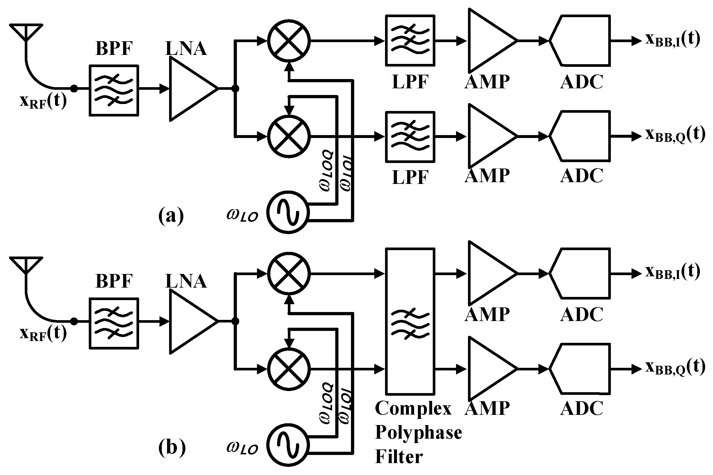
Figure 3.
Block diagram of complex bandpass continuous-time delta-sigma modulator.
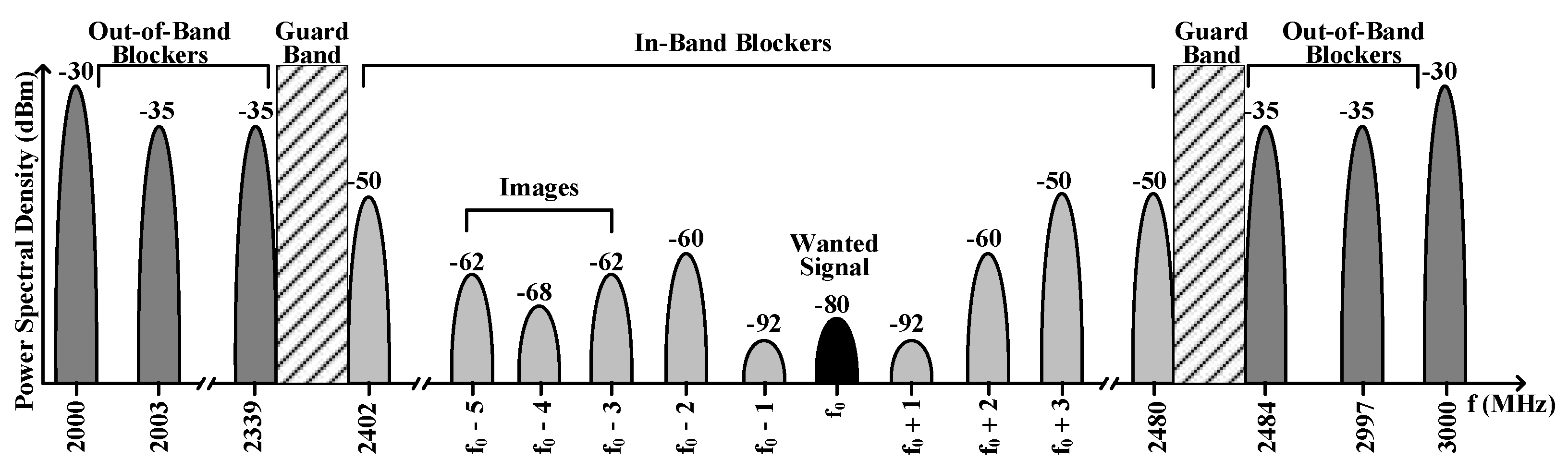
Figure 4.
Block diagram of complex bandpass continuous-time delta-sigma modulator.
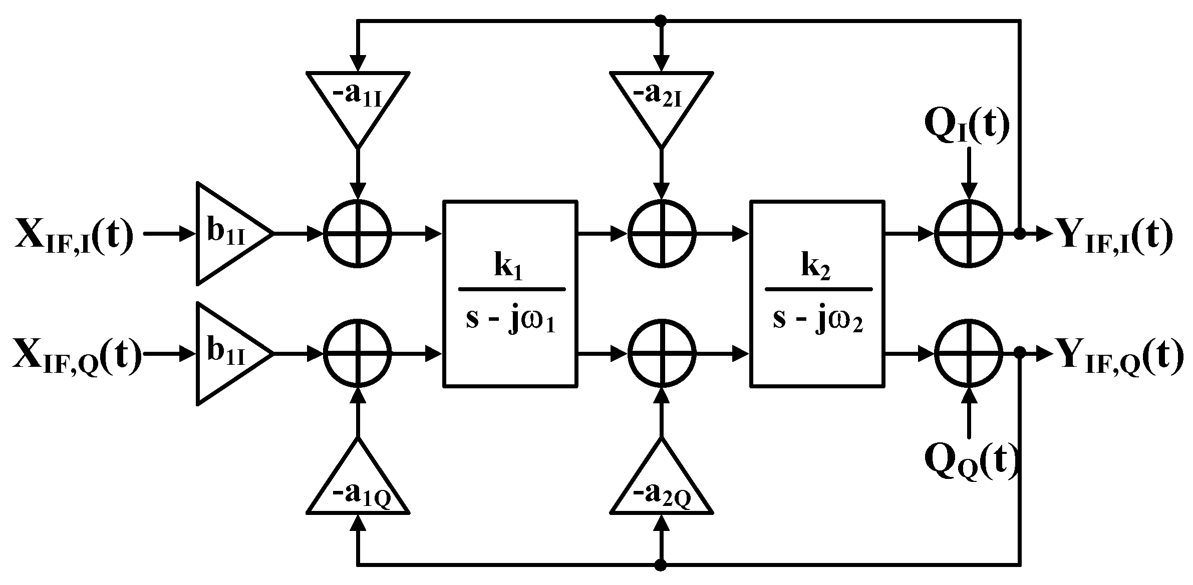
Figure 5.
Block diagram and transfer functions H (jω) of QBP-CTΣΔM.
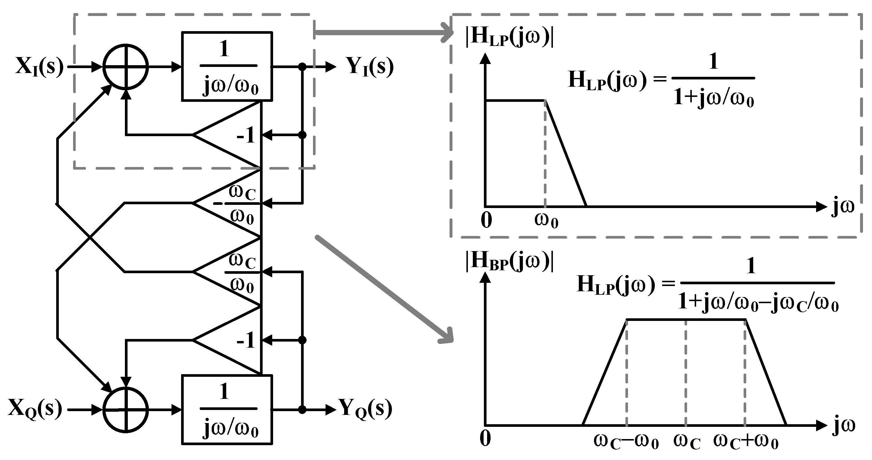
Figure 4.
Block diagram and transfer functions H (jω) of QBP-CTΣΔM.
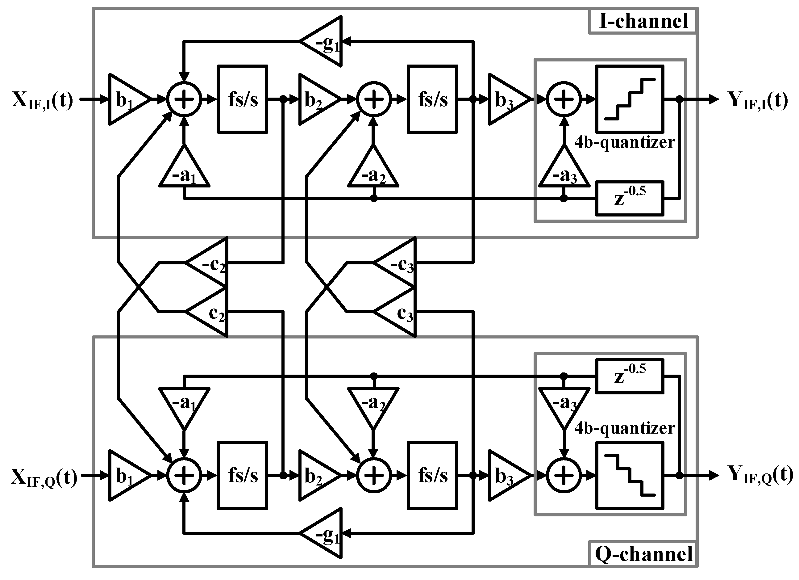
Figure 7.
(a) active-RC and (b) Gm-C integrators and (c) transconductance amplifier (OTA).
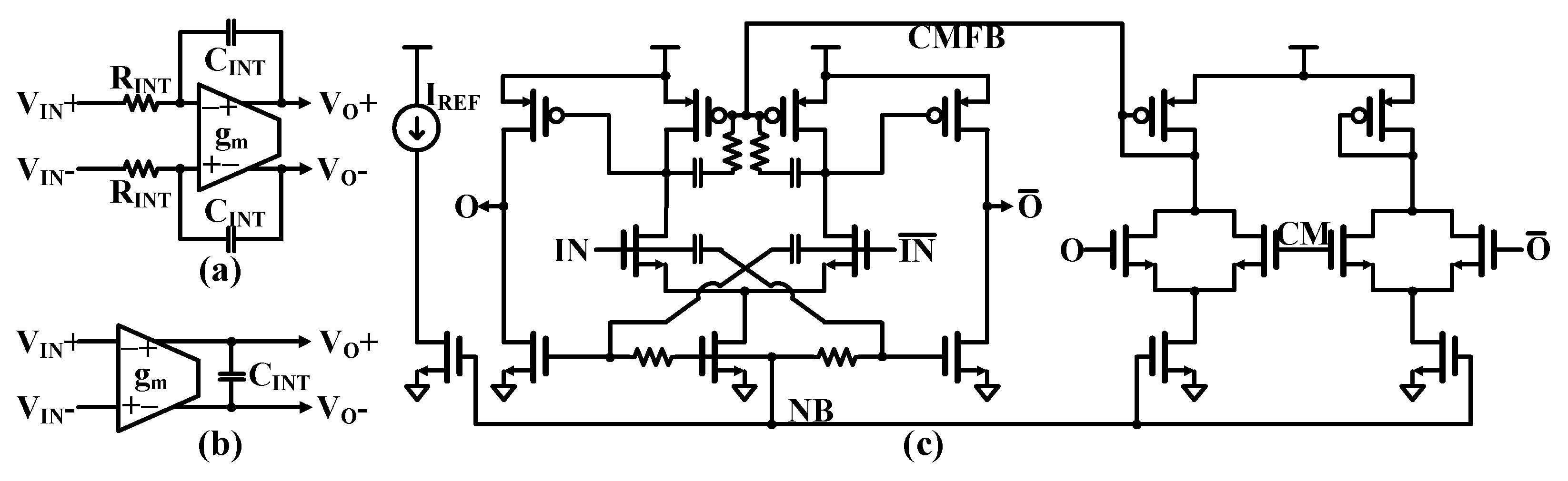
Figure 8.
SAR-type delta modulator operation for feedback gains of (a) < 1 and (b) > 1.
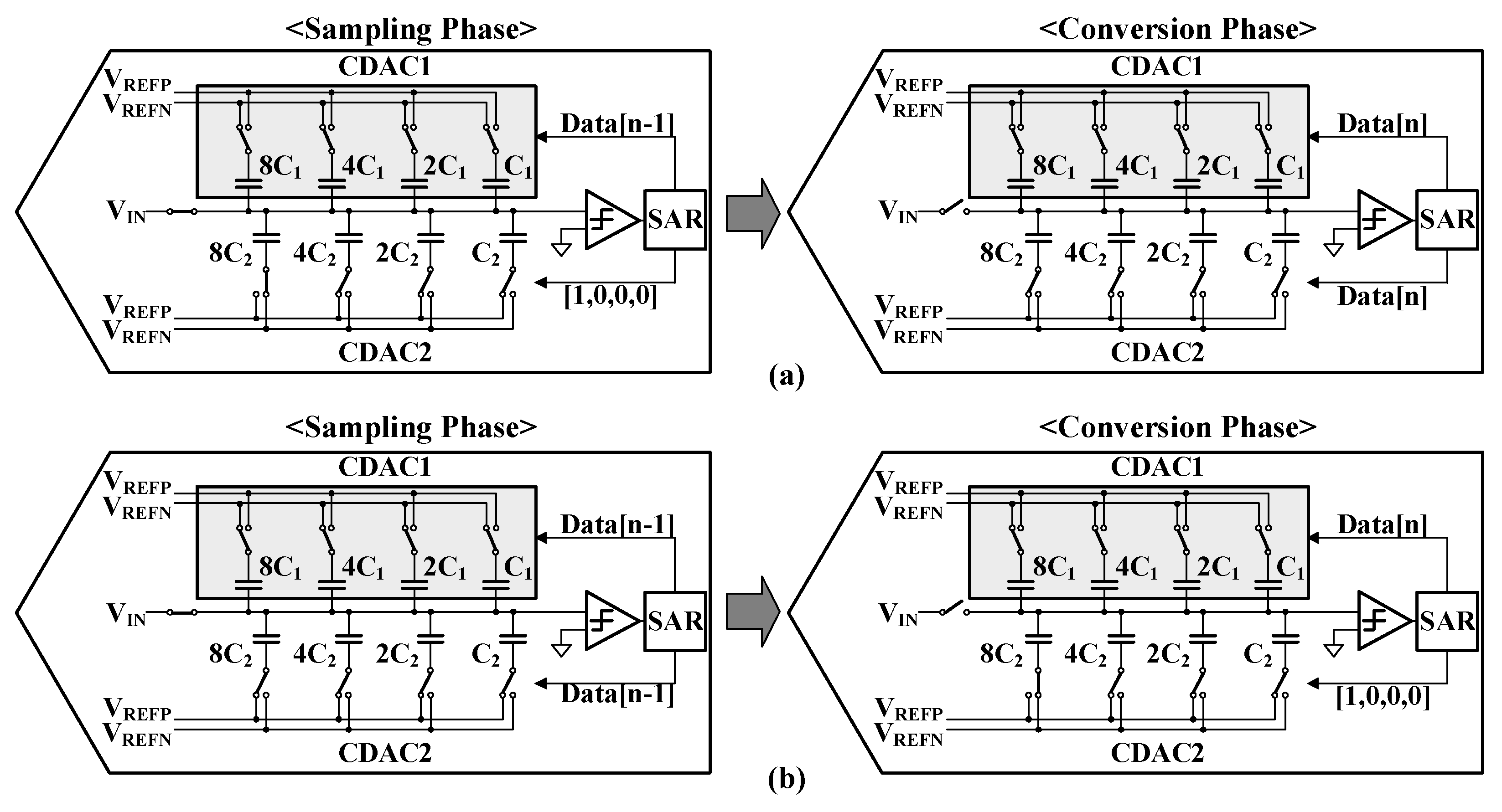
Figure 9.
(a) layout view of capacitor array of CDAC and (b) StrongARM comparator.
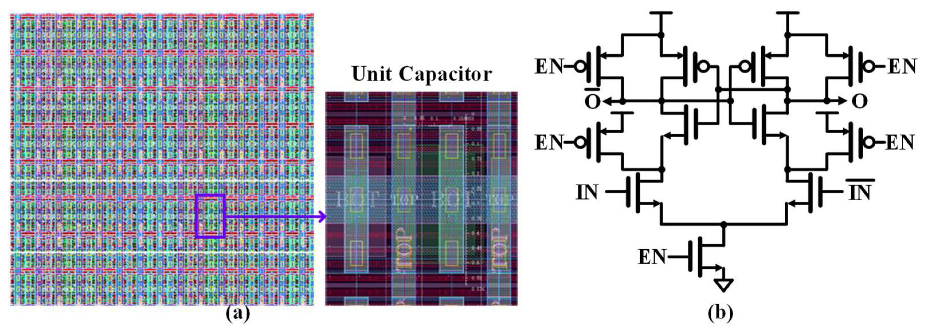
Figure 10.
(a) Chip microphotograph and (b) layout view of the QBP-CTΣΔM ADC.
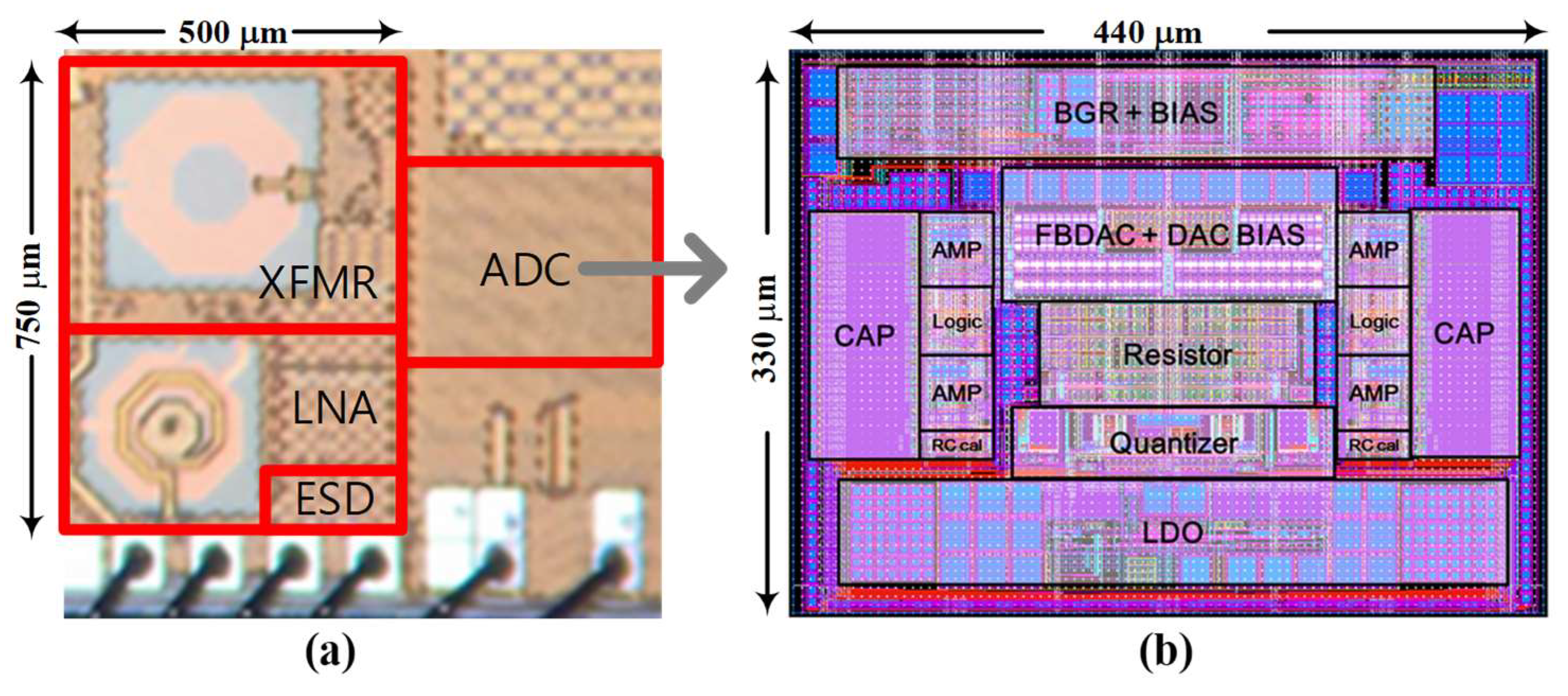
Figure 11.
Output spectrum of the RX output with low-IF signal at 1.5MHz.
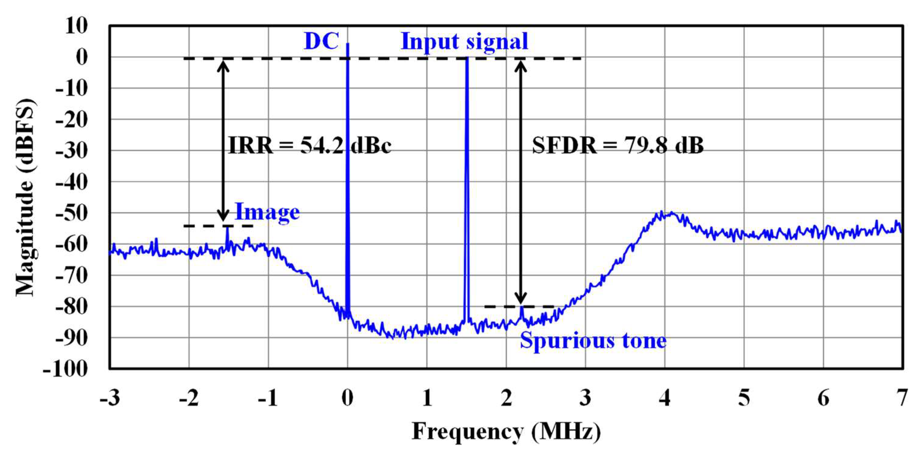
Figure 12.
Measured SNR and SNDR for various input voltages.
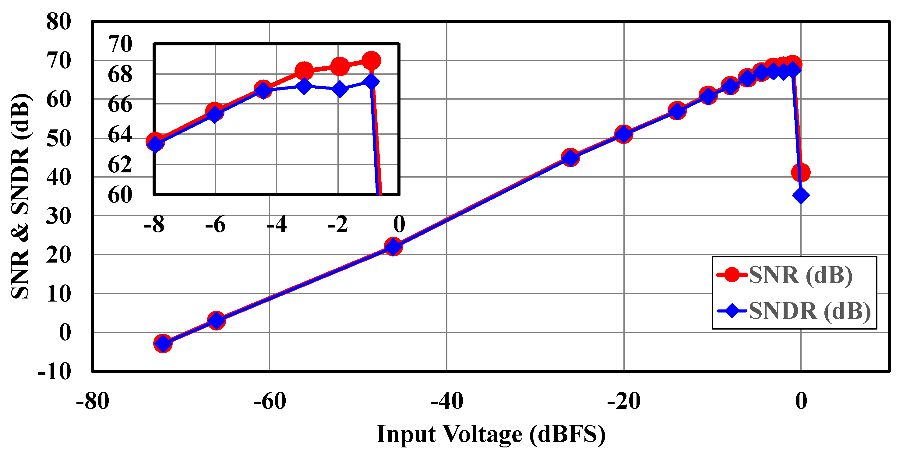
Figure 13.
Measured intermodulation performance.
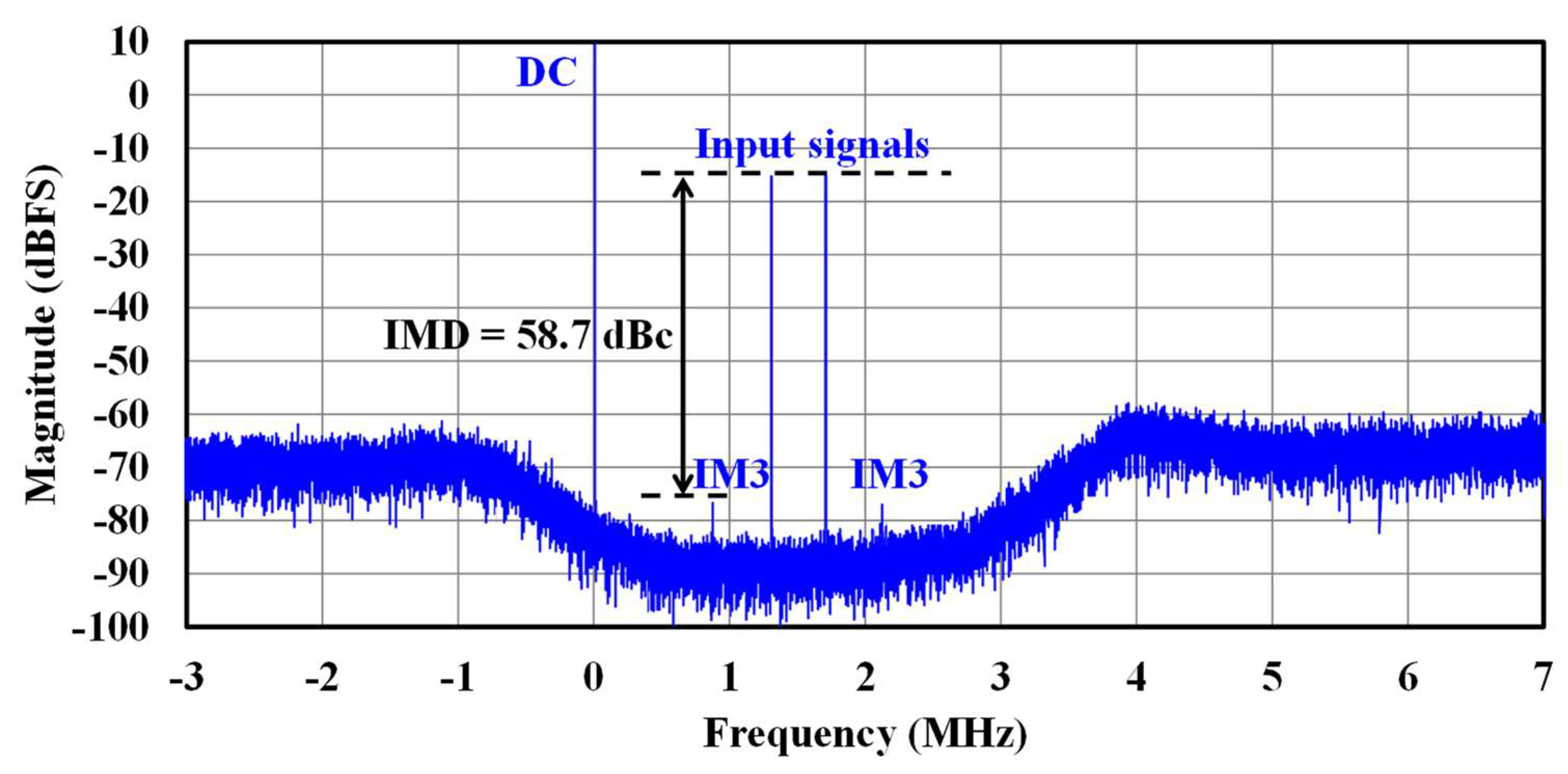

Table 1.
Performance summary of the proposed TX and comparisons to the state-of-the arts.
|
This Work |
[30] MEJ23 |
[31] CICC21 |
[32] ISSCC18 |
[33] TMTT17 |
[34] TVLSI16 |
|
| Technology (nm) | 28 | 180 | 180 | 160 | 180 | 65 |
| System | BLE | IoT Sensor | IoT Sensor | IoT Sensor | GNSS | BLE |
| RX Architecture | Low-IF | − | − | − | Low-IF | Low-IF |
| ADC Type | CT-QΣΔM | DT-ΣΔM | DT-ΣΔM | SAR+ DT-ΣΔM |
CT-QΣΔM | CT-QΣΔM |
| ADC ENOB (bit) | 10.9 | 16.1 | 14.5 | 19.3 | 10.0 | 10.2 |
| Sampling frequency (MHz) |
32 | 2.5 | 0.2 | 2 | 460 | 200 |
| Signal BW (MHz) | 2 | 0.01 | 0.0008 | 0.001 | 33 | 5 |
| IRR (dBc) | 54.2 | − | − | − | 59.3 | 59.6 |
| DR (dB) | 70.3 | 102.6 | 94.1 | 120.3 | 64 | 74.3 |
| SNDR (dB) | 67.5 | 98.6 | 89.3 | 118.1 | 62.1 | 62.9 |
| SNR (dB) | 68.9 | 101.5 | 91.9 | 119.1 | 64.5 | 64.4 |
| Supply Voltage (V) | 1.0 | 1.8 | 1.5 | 1.8 | 1.8 | 1.2 |
| ADC Power (mW) | 0.81 | 1.3 | 0.004 | 0.28 | *25.4 | 4.2 |
| ADC Area (mm2) | 0.145 | 0.648 | 0.75 | 0.25 | 0.73 | 0.39 |
| FOMS (dB) | 164.3 | 171.5 | 177.1 | 185.8 | 155.1 | 165.1 |
| FOMW (fJ/conv.) | 103.2 | 934.2 | 104.8 | 213.1 | 369.8 | 368.1 |
| * Estimation by subtracting other circuit power consumption from the total receiver power | ||||||
Disclaimer/Publisher’s Note: The statements, opinions and data contained in all publications are solely those of the individual author(s) and contributor(s) and not of MDPI and/or the editor(s). MDPI and/or the editor(s) disclaim responsibility for any injury to people or property resulting from any ideas, methods, instructions or products referred to in the content. |
© 2025 by the author. Licensee MDPI, Basel, Switzerland. This article is an open access article distributed under the terms and conditions of the Creative Commons Attribution (CC BY) license (https://creativecommons.org/licenses/by/4.0/).
Copyright: This open access article is published under a Creative Commons CC BY 4.0 license, which permit the free download, distribution, and reuse, provided that the author and preprint are cited in any reuse.


