
Submitted:
16 September 2025
Posted:
17 September 2025
You are already at the latest version
Abstract
This paper proposed an adaptive bandwidth PLL that integrates Integer-N and Fractional-N switching for energy-efficient RF synthesis in IoT and mobile applications. The architecture exploits wide-bandwidth Integer-N mode for rapid lock acquisition, then seamlessly transitions to narrow-bandwidth Fractional-N mode for high-resolution synthesis and noise optimization. The architecture features a bandwidth-reconfigurable loop filter with intelligent switching control that monitors phase error dynamics. A novel adaptive digital noise filter mitigates ΔΣ quantization noise, replacing conventional synchronous delay lines. The multi loop structure incorporates a high resolution digital phase detector to enhance frequency accuracy and minimize jitter across both operating modes. With 180 nm CMOS technology, the PLL consumes 13.2 mW while achieving −119 dBc/Hz in-band phase noise, 1 psrms integrated jitter. Lock time improvements of 70% are demonstrated compared to single-mode implementations, making it suitable for high-precision, low-power wireless communication systems requiring agile frequency synthesis.
Keywords:
Adaptive bandwidth PLL
; fractional-N/integer-N switching
; low-power frequency synthesis
; phase noise optimization
; ΔΣ noise
; multi-loop PLL
1. Introduction
The exponential growth of Internet of Things (IoT) devices and mobile communication systems has created unprecedented demands for frequency synthesizers about fast frequency acquisition, high spectral purity, and power efficiency [1,2,3]. Modern wireless standards such as 5G NR, Wi-Fi 6E and emerging sub-6GHz IoT protocols, require fast-locking frequency synthesizer with a lock time in the microsecond range, while maintaining phase noise performance below -100 dBc/Hz at critical offset frequencies for adjacent channel interference rejection [4,5].
Traditional PLL based frequency synthesizers often rely on two main architectures: Integer-N and Fractional-N, each type with its own advantages and disadvantages. With Integer-N PLL structure has superior phase noise performance and simplified loop dynamics, but is limited by coarse frequency resolution, as this resolution depends on the reference frequency [6,7,8,9]. Conversely, the Fractional-N architecture overcomes this limitation by using delta-sigma modulation on the feedback divider to create fractional multiplication ratios, thereby significantly improving frequency resolution. However, this approach introduces quantization noise, which degrades signal purity, especially within the loop bandwidth region [10,11]. Recent implementations have sought to mitigate these drawbacks by using advanced modulators, digital pre-distortion techniques, and complex loop filter designs [12,13,14]. Nevertheless, these methods often only solve one part of the performance trade-off problem and can lead to a significant increase in both power consumption and circuit complexity.
The explosion of wireless systems, energy-harvesting IoT nodes, wearable devices, and mobile devices has set a requirement to intelligently balance performance metrics with power consumption levels, especially when they must operate in strict temperature conditions [15,16]. Furthermore, the popularity of multi-standard transceivers demands that frequency synthesizers must be capable of supporting a very diverse range of channel spacings on the same single hardware platform [17,18]. This requirement spans from narrow-band IoT applications (≤25 kHz) to wideband mobile systems (≥100 MHz).
Some recent proposed have explored adaptive phase-locked loop (PLL) architectures to address performance challenges [19,20]. These solutions include PLLs that can switch bandwidth by using reconfigurable loop filters, or dual-mode Integer-N/Fractional-N implementations for specialized applications [21,22]. Beside, the voltage-controlled oscillator (VCO) - the core frequency-generating component - is still a key factor, determining overall PLL performance in terms of phase noise, power consumption, and area [23,24]. The traditional LC-tank VCOs bring excellent phase noise performance but take up large area and have a limited tuning range. Meanwhile, ring oscillator-based VCOs are more compact but have significantly poorer phase noise characteristics. Recently, inductorless VCO structures have emerged as a promising alternative solution to balance between area and acceptable noise performance [25,26]. Nevertheless, current methods still have a number of serious limitations: suboptimal switching mechanisms (based on predetermined time), inadequate noise filtering in fractional mode, and a limited reconfigurable bandwidth range. These solutions also often consume a lot of energy for mode switching and control circuitry(1) suboptimal switching mechanisms that rely on predetermined timing rather than real-time loop dynamics, (2) inadequate noise filtering in fractional mode leading to spurious tone generation, (3) limited bandwidth reconfiguration range constraining adaptation flexibility, (4) substantial power overhead associated with mode switching and control circuitry, and (5) VCO designs that either consume excessive silicon area or compromise phase noise performance [27,28]. Moreover, conventional approaches lack intelligent switching algorithms that can predict optimal transition points based on phase error dynamics, resulting in unnecessary switching overhead and potential stability issues [29,30].
This paper presents a new adaptive bandwidth PLL architecture, seamlessly integrating Integer-N and Fractional-N synthesis modes with smart switching control to achieve an optimal energy-performance balance in diverse operating conditions. The proposed system exploits wideband Integer-N operation for quick lock acquisition, then dynamically switches to narrowband Fractional-N mode for high-resolution synthesis and improved noise performance. The main proposals include: (1) a reconfigurable bandwidth loop filter with continuous adaptation capability over more than two decades of bandwidth variation, (2) a smart switching controller monitoring real-time phase error dynamics to predict optimal mode transitions, (3) a new adaptive digital noise filter with the ability to effectively suppress quantization noise without requiring a conventional synchronous delay line, and (4) a multi-loop architecture combining high-resolution digital phase detection to enhance frequency accuracy in both operating modes.
The remainder of this paper is organized as follows: Section II presents the architectural overview and theoretical analysis of the proposed adaptive PLL system. Section III details the circuit implementation including the bandwidth-reconfigurable loop filter, intelligent switching controller, and adaptive noise filtering techniques. Section IV provides comprehensive experimental validation demonstrating lock time improvement, −119 dBc/Hz in-band phase noise, 1 integrated jitter, and 13.2 mW power consumption in 180 nm CMOS technology. Finally, Section V concludes with performance comparisons and discusses applications in next-generation wireless communication systems.
2. Proposed Architecture and System Analysis
2.1. System Overview
The proposed adaptive bandwidth PLL architecture, illustrated in Figure 1 , uses a dual-mode synthesis approach, dynamically optimizing between Integer-N and Fractional-N operations based on real-time system requirements.
This architecture operates based on a reference frequency, , which acts as a stable input clock. The core loop consists of a phase-frequency detector (PFD), a charge pump (CP), a loop filter (LF), and a voltage-controlled oscillator (VCO), forming a type-II feedback system that locks the output frequency to a multiple of . Essentially, the system consists of two main loops that work in close coordination, creating a hybrid architecture of wideband integer-N frequency multiplication and fractional-N synthesis, aiming to achieve an optimal balance between wide bandwidth, low phase noise and high resolution.
The wideband Integer-N path uses an integer divider () in both the reference and feedback branches, supporting coarse, wideband tuning with minimal phase noise accumulation. The reference signal is divided to create at the PFD input, enabling fast acquisition and wide frequency coverage. Creating a high phase comparison frequency for the main loop is a key technique to reduce in-band phase noise. With the Fractional-N Path, not only this path introduces fractional division via a programmable divider that switches between N and N+1, modulated by a delta-sigma modulator () and summation node () but also Integrated in parallel. A dedicated noise filtering block in the feedback loop suppresses high-frequency quantization noise, ensuring compliance with stringent spectral mask requirements in critical applications. The steady-state voltage signals at the circuits’s several nodes are shown in Figure 2 with N = 4, M = 5 and = 0.2. In this configuration, the divider must perform a total division of . The diagram clearly shows how the accumulator, prescaler, and static divider cooperate to generate the output pulse sequence with the exact period corresponding to the required division ratio. As clock pulses enter, the accumulator increments and controls the prescaler to switch states after each group of pulses, while the static divider ensures a regular repetition cycle. As a result, at the divider output, the input pulses are grouped and reset precisely every 21 cycles, matching the integer-N division requirement. This figure provides a visual proof that the hybrid PLL architecture can reuse the same accumulator structure originally intended for fractional-N mode to perform integer-N division, effectively replacing the conventional swallow counter while still maintaining the accuracy and stability of the phase-locked loop.
2.2. Dual-Mode Switching Operating Principle
Figure 3 shows the proposed dual-mode switching operating principle. The integer-N mode is engaged by disabling the fractional component, such as setting the fractional input = 0 in the modulator. The divider remains fixed at N (or ), effectively bypassing the dithering and summation. The output frequency simplifies to , where the dual M dividers (one in reference, one in feedback) result in an effective multiplication factor of . With no quantization noise from , in-band phase noise is minimized. The wideband aspect comes from the high PFD comparison frequency (), which expands loop bandwidth (where is PFD/CP gain and is VCO sensitivity). This suppresses VCO noise over a broader offset range, achieving figures like 100 dBc/Hz at 1 kHz offset.
On the hand, the Fractional-N mode enabled by providing a non-zero () to the modulator, which generates a bitstream to toggle the divider between N and . The effective division ratio becomes fractional: , yielding . Frequency resolution is for k-bit , enabling sub-Hz steps. Quantization noise from dithering is shaped by the and nd pushed to high frequencies. The LF (low-pass filter) and dedicated "Noise Filtering" block (possibly a notch filter) attenuate this noise, keeping spurs below −70 dBc. The phase perturbation (with ) helps linearize PFD response and reduce dead-zone effects. The overall dual-mode switching can be expressed as Equation (1):
where, is the transition point the intelligent controller. This controlled handover ensures that bandwidth shrinks smoothly from wide to narrow without inducing jitter peaking or instability. Compared to conventional PLLs with a fixed narrow bandwidth (which offer low noise but long lock time) or a fixed wide bandwidth (which achieve fast locking but suffer from degraded noise performance), the dual-mode architecture optimizes both requirements. As a result, the lock time is significantly shortened, the in-band noise is improved in the steady state, and the reference spurs are maintained at a low level.
Figure 4 illustrates the hypothetical evolution of the phase error in time, comparing the hybrid PLL (solid curve) with a conventional integer-N PLL (dashed curve). In the hybrid case, the loop initially operates in the wide-band integer-N mode, enabling rapid reduction of the phase error and thus a much faster lock process. Once the loop approaches steady state, it switches to the narrow-band fractional-N mode, allowing smoother convergence and lower in-band noise. By contrast, the conventional integer-N PLL shows a slower decay of the phase error, highlighting the hybrid architecture’s ability to simultaneously achieve fast acquisition and improved steady-state noise performance.
3. Circuit Implementation
3.1. Bandwidth-Reconfigurable Loop Filter
The loop filter in the proposed PLL is implemented as a Type-II second-order filter with a zero, featuring bandwidth reconfigurability through the insertion of a programmable capacitor branch. In the linear model, the loop dynamics are characterized by the natural frequency and the damping factor . For an RC filter with a single zero, the transfer function can be expressed as Equation (2):
The open-loop gain (Equation (3)) is given by:
where denotes the gain of the PFD/charge pump, is the VCO sensitivity, and N is the effective division ratio. Matching the characteristic equation to the standard second-order form yields in Equation (4):
To enable bandwidth reconfiguration, an auxiliary capacitor is switched in parallel with . Thus with Equation (5),
leading to two distinct natural frequencies (Equation (6)):
In the wide-band mode, increases significantly, reducing the lock time according to Equation (7)
Conversely, the narrow-band mode is activated once the PLL approaches steady state to improve in-band noise performance. To avoid jitter peaking during the mode transition, the ratio must be maintained constant, which can be achieved by scaling accordingly or by employing a tunable OTA to shift proportionally.
From a noise perspective, the VCO noise transfer follows Equation (8):
indicating that expanding the loop bandwidth suppresses VCO noise over a broader offset range. By contrast, reference noise, PFD/CP noise, and quantization noise pass through the loop according to Equation (9):
so narrowing the bandwidth effectively reduces their impact at the output. Furthermore, quantization noise from the modulator is further suppressed by an additional noise-filtering block (Equation (10)):
Finally, the transition between the two modes is governed by phase error thresholds. When both the phase error magnitude and its slope fall below predefined thresholds for a holding period , the system switches from wide-band to narrow-band operation. This ensures a smooth transition without inducing overshoot or spurious tones. Schematic diagram of a zero-biased second-order Type-II loop filter with a programmable condenser arm. The condenser arm is switched on/off via a switch to vary the time constant, allowing bandwidth reconfiguration: widening during the lock-in phase to shorten the convergence time, and narrowing during steady state to improve in-band noise that shows Figure 3
3.2. Intelligent Switching Controller
To fully exploit the benefits of the reconfigurable loop filter, the system requires an Intelligent Switching Controller (ISC). In conventional PLL designs, bandwidth or mode changes are typically performed through static logic signals or manual control, which can easily lead to instability or spur generation when the transition is not synchronized. In contrast, the ISC in the proposed architecture is capable of monitoring the dynamics of the phase error and the quantization noise level from the modulator, thereby making real-time adaptive decisions for mode switching.
In principle, the intelligent controller continuously monitors the output of the phase detector, tracking both the frequency and the amplitude of the phase error pulses. When the amplitude of the phase error falls below a predefined threshold and the slope of the phase error also drops below a certain limit, the ISC determines that the loop has approached a near-lock state. At this point, the loop filter is commanded to narrow its bandwidth, thereby improving noise performance. If abnormal oscillations or jitter peaking occur during the transition, the ISC can automatically reverse the configuration and restore the wide-bandwidth mode to maintain loop stability.
A key contribution of the ISC is the exploitation of modulator outputs to predict in-band noise levels. Rather than relying solely on the magnitude of the phase error, the controller also considers the spectral properties of the sequence, enabling bandwidth switching decisions to be made more appropriately and avoiding premature or delayed reconfiguration. This approach significantly reduces spurs caused by quantization noise in Fractional-N mode, while maintaining fast dynamic response in Integer-N mode.
From an implementation perspective, the ISC can be realized as a finite state machine (FSM) combined with a digital monitoring unit. The FSM defines states such as Acquisition, Transition, and Steady-state, while the monitoring unit provides trigger signals based on the mean and variance of the phase error over a defined observation window. Owing to its fully digital architecture, the ISC consumes very low power, is easily integrated on-chip, and does not require complex hardware such as delay lines or auxiliary analog detectors that is shown in Figure 5.
System-level simulations demonstrate that the ISC enables smooth transition from Integer-N mode to Fractional-N mode without introducing significant jitter peaking, while ensuring the stability of the PLL control range. Furthermore, the timely reconfiguration of loop bandwidth shortens the lock time compared to a fixed narrow-bandwidth design and reduces in-band spurs compared to a fixed wide-bandwidth design.
3.3. Adaptive Digital Noise Filter
3.3.1. Quantization Noise Suppression
To realize a high-performance digital delta-sigma modulator in Figure 6, the proposed hybrid architecture splits the input signal processing path () into two parallel streams to optimize for speed and noise performance. The processing path for the Low-Significant Bits (LSBs), which include bits from to , uses a pipelined accumulation structure consisting of three 4-bit adders and their corresponding registers. This pipelining technique circumvents the critical transfer-memory path, allowing the entire circuit to operate at gigahertz clock frequencies. Furthermore, a dithering signal is introduced to linearize the quantization process and suppress spurious harmonics.
At the same time, the modulator core processes the Most Significant Bits (MSBs), from to , through a complex, high-order feedback integrator structure. This structure, which consists of an 11-bit adder and two 13-bit adders, aggressively shapes the Noise Transfer Function (NTF). The weighted feedback coefficients (represented by ×4 and /4 bit-shifting operations) are optimized to place the NTF’s poles, thereby ensuring loop stability and limiting the out-of-band gain. At the final stage, in addition to the main 1-bit output (out) used to control the frequency divider, the architecture also extracts a multi-bit word () from the accumulator’s internal state. This signal enables the implementation of advanced quantization error cancellation techniques via a peripheral block such as DTC, achieving extremely high spectral purity. In terms of hardware resources, the design requires a total of six adders and approximately 50 single-bit registers (flip-flops). So, noise transfer function of the 3-order is shown by Equation (11):
Figure 7 illustrates the calculated Figure of Merit (FoM) of the third-order modulator in (a), and the simulated SNR and SNDR characteristics of the proposed PLL as a function of the input amplitude in (b).
3.3.2. Noise Filtering Architecture
This architecture presents an an advanced hybrid noise-filtering solution, combining analog and digital processing within a two-stage structure, specifically designed to suppress the complex quantization noise generated by modulators. The core principle is an effective partitioning of the filtering task: the analog stage handles the coarse, high-power processing, while the digital stage performs the fine, precise, and flexible processing.
The first stage, operating entirely in the analog domain, has the primary objective of suppressing the out-of-band noise component, where the spectral power density of the quantization noise is highest. To achieve this, a continuous-time notch filter is used. The biggest challenge in implementing this filter on a CMOS integrated circuit is the area limitation and the low quality factor (Q-factor) of passive spiral inductors. The applied technical solution is to build an active inductor based on a gyrator structure, which is formed from two transconductors (). This structure allows for the synthesis of an equivalent inductance () according to the formula Equation (12):
where is a terminating capacitor and , are the transconductance values. This technique not only creates a virtual inductor with a large value and a high Q-factor within a compact area, but also allows for the adjustment of the notch frequency by changing the value, providing a certain degree of flexibility to this coarse filtering stage.
The second stage, operating in the digital domain, is designed to handle the remaining noise components, especially the spurious tones that can randomly appear inside the signal band (in-band). This stage requires high precision and programmability; therefore, a Switched-Capacitor (SC) Filter is used in Figure 8 and Figure 9 is shown Integrated noise contribution versus Fractional-N PLL reference frequency.
3.4. Multi-Loop Architecture with High-Resolution Phase Detector
Figure 10 shows the proposed multi-loop PLL architecture, Two XOR phase detectors are used to replace the conventional PFD. The choice of XOR arises from its notable advantages: low hardware complexity, extremely low power consumption, and the ability to generate a phase error signal with high linearity within the ±90° range. In particular, by combining two XOR detectors operating in different modes, the system can simultaneously achieve an extended dynamic range and improved phase detection resolution.
In the multi-loop structure, one XOR detector is configured for the wide-bandwidth Integer-N loop, allowing the circuit to quickly converge toward the lock state thanks to its fast response to large phase errors. The second XOR detector is connected to the narrow-bandwidth Fractional-N loop, operating in the steady state after the PLL has nearly locked, and is responsible for fine phase adjustment with high resolution. By dividing the roles between the two XORs, the architecture exploits the fast convergence of the Integer-N loop while ensuring optimal noise characteristics in the Fractional-N loop.
To avoid spur generation and jitter peaking during the transition, the phase error signals from both XOR detectors are fed into the Intelligent Switching Controller. This controller simultaneously monitors the amplitude of large phase errors (reported by the first XOR) and small phase errors (reported by the second XOR). When the error is determined to lie within the narrow linear region, the system gradually transfers control to the Fractional-N loop. This combination ensures that the transition between the two loops occurs smoothly without causing instability.
Another important advantage of using XOR detectors instead of the conventional PFD is the significant reduction in area and power overhead. XOR requires only a small number of CMOS transistors, does not need complex reset circuitry, and does not generate wide pulses (dead-zone free). This makes it particularly suitable for IoT and mobile applications, where ultra-low power and high integration are essential.
Simulation results show that the multi-loop architecture using two XOR detectors can achieve a much faster lock time compared to a single-loop PLL using only one XOR, while maintaining low phase noise in the Fractional-N mode. This combination demonstrates that even with a simple phase detection element such as XOR, when properly deployed in a multi-loop structure, it can achieve performance comparable to or better than more complex PLL designs.
3.5. Compact Inductorless VCO
The VCO architecture consists of three main blocks: the bias current control circuit, the oscillator circuit, and the pulse-width modulation (PWM) circuit as illustrated in Figure 11. The focus of the whole circuit design is the bias current control circuit, which regulates the current levels supplied to the oscillator stages based on the input bias voltages VBIAS, VOS1, VOS2, VOS3. These voltages are used to independently adjust the bias conditions of the three delay stages in the ring oscillator, ensuring precise tuning and optimization of the oscillator’s performance.
The oscillator circuit is a ring oscillator com-posed of three stages, where the oscillation frequency is determined by the control voltage VVCT.
The bias controlled current circuit includes four current sources which are biased by a common control voltage VBIAS. By controlling the current levels in the inverters, the frequency of oscillation is adjusted. This configuration ensures precise tuning and efficient operation of the VCO while maintaining stability and linearity in its response to control inputs.
The three-stage ring oscillator in the proposed bias current-controlled VCO is designed using a combination of inverters and transmission gates to achieve precise frequency tuning, as illustrated in Figure 12. Each stage of the ring oscillator consists of a standard CMOS inverter paired with a transmission gate. The control voltage VVCT plays a central role in this configuration, as it modulates the resistance of the transmission gates by controlling their gate voltage. This modulation directly affects the delay introduced by each oscillator stage. As VVCT increases or decreases, the resistance of the transmission gates adjusts accordingly, either increasing or decreasing the propagation delay in each stage of the oscillator. Since the total delay of the ring oscillator is the sum of the delays in all three stages, this mechanism provides an effective means to control the oscillation frequency of the VCO.
The cycle and frequency responses of the proposed three-stage VCO structure with a current control circuit, corresponding to variations in the control voltage VVCT from 0 to 1.8 V, are illustrated in Figure 13(a). The entire system is designed and simulated using the 180 nm CMOS process, occupying an active chip area of 0.001 mm2. Figure 13(b) presents the phase noise performance of the VCO at 1 MHz of offset frequency and the oscillation frequency as a function of the control voltage VVCT.
This control voltage fine-tunes the delay of each stage, enabling the generation of a stable frequency output. The current control and oscillator circuits are closely integrated to achieve linear tuning behavior and minimize phase noise. Finally, the PWM circuit enhances the output signal by modulating its duty cycle. This block refines the output waveform, reducing the jitter and improving spectral purity. All blocks receive their control power from a dedicated power supply block, ensuring stable operation.
4. Experimental Results
The proposed dual-mode hybrid PLL with a bandwidth-reconfigurable loop filter and intelligent switching controller has been fabricated in a standard 180-nm CMOS process. The die micrograph is shown in Figure 14, occupying an active area of 0.035 mm2. The prototype employs a 25.5-MHz crystal oscillator as the reference and covers an output frequency range from 2.9 GHz to 3.2 GHz. Operating from a 1.8-V supply, the PLL consumes a total of 8.6 mW in Fractional-N steady-state mode and 4.6 mW in Integer-N acquisition mode. Within the total power, the VCO accounts for 2.3 mW, the divider and modulator consume 3.13 mW, the charge pump and loop filter driver dissipate 1.0 mW, while the digital ISC and auxiliary noise-filtering circuits draw 0.2 mW and 0.5 mW, respectively.
The measured output spectra are depicted in Figure 15 With the adaptive noise filtering enabled, reference spur suppression improves by 15 dB at a 40-MHz offset, with the largest spur maintained below dBc. The measured reference spur of PLL achieved dBc in Figure 16 and -119 dBc/Hz phase noise at 100 KHz Figure 17 . These results confirm that the ISC enables seamless mode transition without introducing significant jitter peaking.
Table 1 summarizes the measured performance of the proposed architecture and compares it with representative state-of-the-art Fractional-N synthesizers, after scaled to 28 nm process following [35]. Owing to its dual-mode operation, the prototype achieves both a fast lock time of less than 5 s (benefiting from the wide-band acquisition mode) and low in-band noise comparable to LC-VCO-based designs. The overall figure-of-merit (FoM) of −232.22 dB is competitive with state-of-the-art synthesizers, while the elimination of large on-chip inductors enables a compact and energy-efficient solution for mobile and IoT RF applications.
5. Conclusions
This paper introduces a novel dual-mode hybrid phase-locked loop architecture that marries the best features of both Integer-N and Fractional-N synthesis. It achieves this using a reconfigurable loop filter and a smart intelligent switching controller. The reconfigurable loop filter dynamically changes the loop bandwidth. This allows the PLL to operate in two distinct modes: 1) Wide-band Integer-N mode: this mode provides rapid signal acquisition, meaning it locks onto the desired frequency very quickly; 2) Narrow-band Fractional-N mode: this mode minimizes in-band noise, resulting in a cleaner output signal.
The intelligent switching controller is a key innovation. It monitors both the phase error and the noise from the modulator to manage the transition between these two modes. This adaptive control ensures the switch is seamless, preventing unwanted jitter peaking and minimizing spurious tones that can degrade signal quality. A prototype of the proposed PLL was built using a 180-nm CMOS process. It operates in the 2.9-3.2 GHz frequency range and delivers impressive performance of: 1) Lock time: less than 5 microseconds; 2) In-band phase noise: −119 dBc/Hz in Fractional-N mode; 3) Spur levels: below −62.7 dBc. The overall FoM is an impressive −228.8 dB, which is highly competitive with other advanced designs. Unlike many other high-performance synthesizers, this design avoids the need for large and power-hungry LC-based inductors, making it compact and energy-efficient.
These results confirm that the proposed architecture is a viable solution for modern RF systems, such as IoT and mobile communication devices, where a small footprint and low power consumption are crucial. Future research will explore scaling the design to more advanced manufacturing processes (sub-10 nm) and using machine learning to further optimize its performance.
Author Contributions
Writing—original draft, Nguyen, T.V.H.; Writing—review and editing, Nguyen, T.V.H. and C.-K.P. All authors have read and agreed to the published version of the manuscript
Funding
This research received no external funding.
Acknowledgments
The VLSI chip in this study has been fabricated through the activities of VLSI Design and Education Center (VDEC), the University of Tokyo, in collaboration with Synopsys, Inc., Cadence Design Systems Inc., Mentor Inc., Rohm Semiconductor (ROHM), and Nippon Systemware Co., Ltd.
Conflicts of Interest
The authors declare no conflicts of interest
References
- Nguyen, T.V.H.; Pham, C.-K. An Overview of Phase-Locked Loop: From Fundamentals to the Frontier. Sensors 2025, 25, 5623. [Google Scholar] [CrossRef]
- Song, H.-G.; Park, K.; Park, J.-Y.; Kwon, T.-H.; Seo, J.-S.; Jeon, S.-W. 5G NR Performance Evaluation Under Phase Noise Distortion for 52.6 GHz to 71 GHz. In Proceedings of the 2021 International Conference on Information and Communication Technology Convergence (ICTC), Jeju Island, Republic of Korea, 20–22 October 2021; pp. 607–610. [Google Scholar]
- Guo, H.; Hu, Y.; Chi, T. A 9.05-to-37.0 GHz LO Generator with Magnetic Mode Switching and Tuning-Free Octave-Bandwidth Common Mode Resonator Achieving >190.7dBc/Hz FoM. In Proceedings of the 2025 IEEE International Solid-State Circuits Conference (ISSCC), San Francisco, CA, USA, 16–20 February 2025; pp. 560–562. [Google Scholar]
- El-Halwagy, W.; Nag, A.; Hisayasu, P.; Aryanfar, F.; Mousavi, P.; Hossain, M. A 28-GHz Quadrature Fractional-N Frequency Synthesizer for 5G Transceivers With Less Than 100-fs Jitter Based on Cascaded PLL Architecture. IEEE Trans. Microw. Theory Tech. 2017, 65, 396–413. [Google Scholar] [CrossRef]
- Karra, K.S.; V., V. An Ultra-low Phase Noise, Low Power 28GHz Frequency Synthesizer for 5G Applications. In Proceedings of the 2018 15th IEEE India Council International Conference (INDICON), Coimbatore, India, 16–18 December 2018; pp. 1–6. [Google Scholar]
- Chen, H.-W.; Lin, M.-H.; Lu, S.-S. A 24GHz Low Power and Low Phase Noise PLL Frequency Synthesizer with Constant KVCO for 60GHz Wireless Applications. In Proceedings of the 2015 IEEE International Symposium on Circuits and Systems (ISCAS), Lisbon, Portugal, 24–27 May 2015; pp. 2840–2843. [Google Scholar]
- Berber, Z.; Kameche, S.; Benkhelifa, E. Design of Integer-N PLL Frequency Synthesizer for E-Band Frequency for High Phase Noise Performance in 5G Communication Systems. IET Netw. 2020, 9, 151–158. [Google Scholar]
- Kira, A.; Elsayed, M.Y.; Allidina, K.; Chodavarapu, V.P.; El-Gamal, M.N. A 6.7 μW Low-Noise, Compact PLL with an Input MEMS-Based Reference Oscillator Featuring a High-Resolution Dead/Blind Zone-Free PFD. Sensors 2024, 24, 7963. [Google Scholar] [CrossRef]
- Herzel, F.; Ergintav, A.; Sun, Y. Phase Noise Modeling for Integrated PLLs in FMCW Radar. IEEE Trans. Circuits Syst. II Express Briefs 2013, 60, 137–141. [Google Scholar] [CrossRef]
- Riley, T.A.D.; Copeland, M.A.; Kwasniewski, T.A. Delta-Sigma Modulation in Fractional-N Frequency Synthesis. IEEE J. Solid-State Circuits 1993, 28, 553–559. [Google Scholar] [CrossRef]
- Hati, M.K.; Bhattacharyya, T.K. A Constant Loop Bandwidth in Delta Sigma Fractional-N PLL Frequency Synthesizer with Phase Noise Cancellation. Integration 2019, 65, 175–188. [Google Scholar] [CrossRef]
- Feng, L.; Rhee, W.; Wang, Z. A Quantization Noise Reduction Method for Delta-Sigma Fractional-N PLLs Using Cascaded Injection-Locked Oscillators. IEEE Trans. Circuits Syst. II Express Briefs 2022, 69, 2448–2452. [Google Scholar] [CrossRef]
- Levantino, S.; Marzin, G.; Samori, C.; Lacaita, A.L. A Wideband Fractional-N PLL With Suppressed Charge-Pump Noise and Automatic Loop Filter Calibration. IEEE J. Solid-State Circuits 2013, 48, 2419–2429. [Google Scholar] [CrossRef]
- Han, J.S.; Eom, T.H.; Choi, S.W.; Seong, K.; Yoon, D.H.; Kim, T.T.; Baek, K.H.; Shim, Y. A Reference-Sampling Based Calibration-Free Fractional-N PLL with a PI-Linked Sampling Clock Generator. Sensors 2021, 21, 6824. [Google Scholar] [CrossRef] [PubMed]
- Lee, J.; Kang, B.; Joo, S.; Lee, S.; Lee, J.; Kang, S.; Jo, I.; Ahn, S.; Lee, J.; Bae, J.; et al. A Low-Power and Low-Cost 14nm FinFET RFIC Supporting Legacy Cellular and 5G FR1. In Proceedings of the IEEE International Solid-State Circuits Conference (ISSCC), San Francisco, CA, USA, 13–22 February 2021; pp. 90–91. [Google Scholar]
- Dartizio, S.M.; Castoro, G.; Gallucci, S.; Rossoni, M.; Moleri, R.; Tesolin, F.; Salvi, P.; Karman, S.; Lacaita, A.L.; Levantino, S. A 380μW and −242.8dB FoM Digital-PLL-Based GFSK Modulator with Sub-20s Settling Frequency Hopping for Bluetooth Low-Energy in 22nm CMOS. In Proceedings of the 2025 IEEE International Solid-State Circuits Conference (ISSCC), San Francisco, CA, USA, 16–20 February 2025; pp. 560–562. [Google Scholar]
- Guan, P.; Jia, H.; Deng, W.; Ma, R.; Liao, H.; Wang, Z.; Chi, B. A 25.0-to-35.9GHz Dual-Layer Quad-Core Dual-Mode VCO with 189.1dBc/Hz FoM and 200.2dBc/Hz FoMT at 1MHz Offset in 65nm CMOS. In Proceedings of the IEEE Custom Integrated Circuits Conference (CICC), San Antonio, TX, USA, 23–26 April 2023; pp. 1–2. [Google Scholar]
- Babaie, M.; Kuo, F.; Chen, H.R. A Fully Integrated Bluetooth Low-Energy Transmitter in 28nm CMOS With 36% System Efficiency at 3 dBm. IEEE J. Solid-State Circuits 2016, 51, 1547–1565. [Google Scholar] [CrossRef]
- Rohde, U.L.; Rubiola, E.; Whitaker, J.C. Digital PLL Synthesizers. In Microwave and Wireless Synthesizers: Theory and Design; Wiley: Hoboken, NJ, USA, 2021. [Google Scholar]
- Rhee, W.; Yu, Z. Phase-Locked Loops, 1st ed.; Wiley-IEEE Press: Hoboken, NJ, USA, 2023. [Google Scholar]
- Woo, K.; Liu, Y.; Nam, E.; Ham, D. Fast-Lock Hybrid PLL Combining Fractional-N and Integer-N Modes of Differing Bandwidths. IEEE J. Solid-State Circuits 2008, 43, 379–389. [Google Scholar] [CrossRef]
- Zhang, B.; Allen, P.E.; Huard, J.M. A Fast Switching PLL Frequency Synthesizer with an On-Chip Passive Discrete-Time Loop Filter in 0.25-μm CMOS. IEEE J. Solid-State Circuits 2003, 38, 855–865. [Google Scholar] [CrossRef]
- Ho, C.-R.; Chen, M. A Digital PLL with Feedforward Multi-Tone Spur Cancelation Loop Achieving <−73 dBc Fractional Spur and <−110 dBc Reference Spur in 65nm CMOS. In Proceedings of the IEEE International Solid-State Circuits Conference (ISSCC), San Francisco, CA, USA, 31 January–4 February 2016; pp. 190–191. [Google Scholar]
- Park, H.; Hwang, C.; Seong, T.; Lee, Y.; Choi, J. A 365fsrms-Jitter and -63dBc-Fractional Spur 5.3GHz-Ring-DCO-Based Fractional- N DPLL Using a DTC Second/Third-Order Nonlinearity Cancelation and a Probability-Density-Shaping δσM. In Proceedings of the IEEE International Solid-State Circuits Conference (ISSCC), San Francisco, CA, USA, 13–22 February 2021; pp. 442–444. [Google Scholar]
- Kong, L.; Razavi, B. A 2.4 GHz 4 mW Integer-N Inductorless RF Synthesizer. IEEE J. Solid-State Circuits 2016, 51, 626–635. [Google Scholar] [CrossRef]
- Gao, X.; Burg, O.; Wang, H.; Wu, W.; Tu, C.T.; Manetakis, K.; Zhang, F.; Tee, L.; Yayla, M.; Xiang, S.; et al. A 2.7-to-4.3GHz, 0.16psrms-Jitter, −246.8dB-FOM, Digital Fractional-N Sampling PLL in 28nm CMOS. In Proceedings of the IEEE International Solid-State Circuits Conference (ISSCC), San Francisco, CA, USA, 31 January–4 February 2016; pp. 174–175. [Google Scholar]
- Jang, S.; Chae, M.; Park, H.; Hwang, C.; Choi, J. A 5.5μs-Calibration-Time, Low-Jitter, and Compact-Area Fractional-N Digital PLL Using the Recursive-Least Squares (RLS) Algorithm. In Proceedings of the IEEE International Solid-State Circuits Conference (ISSCC), San Francisco, CA, USA, 18–22 February 2024; pp. 190–191. [Google Scholar]
- Kim, H.; Jung, W.; Kim, K.; Kim, S.; Choi, W.S.; Jeong, D.K. A Low-Jitter 8-GHz RO-Based ADPLL With PVT-Robust Replica-Based Analog Closed Loop for Supply Noise Compensation. IEEE J. Solid-State Circuits 2022, 57, 1712–1722. [Google Scholar] [CrossRef]
- Liu, Y.-H.; Van Den Heuvel, J.; Kuramochi, T.; Busze, B.; Mateman, P.; Chillara, V.K.; Wang, B.; Staszewski, R.B.; Philips, K. An Ultra-Low Power 1.7–2.7 GHz Fractional-N Sub-Sampling Digital Frequency Synthesizer and Modulator for IoT Applications in 40 nm CMOS. IEEE Trans. Circuits Syst. I Regul. Pap. 2017, 64, 1094–1105. [Google Scholar] [CrossRef]
- Huang, Z.; Jiang, B.; Li, L.; Luong, H.C. A 4.2μs-settling-time 3rd-order 2.1GHz phase-noise rejection PLL using a cascaded time-amplified clock-skew sub-sampling DLL. In Proceedings of the IEEE International Solid-State Circuits Conference (ISSCC), San Francisco, CA, USA, 31 January–4 February 2016; pp. 40–41. [Google Scholar]
- Kong, L.; Razavi, B. A 2.4-GHz 6.4-mW Fractional-N Inductorless RF Synthesizer. IEEE J. Solid-State Circuits 2017, 52, 2117–2127. [Google Scholar] [CrossRef]
- Kang, B.; Kim, Y.; Son, H.; Kim, S. A 0.055 mm2 Total Area Triple-Loop Wideband Fractional-N All-Digital Phase-Locked Loop Architecture for 1.9–6.1 GHz Frequency Tuning. Electronics 2024, 13, 2638. [Google Scholar] [CrossRef]
- He, Y.; Heuvel, J.v.D.; Mateman, P.; Allebes, E.; Traferro, S.; Dijkhuis, J.; Bunsen, K.; Vis, P.; Breeschoten, A.; Liu, Y.-H.; et al. An Injection-Locked Ring-Oscillator-Based Fractional-N Digital PLL Supporting BLE Frequency Modulation. IEEE J. Solid-State Circuits 2022, 57, 1765–1775. [Google Scholar] [CrossRef]
- Zhang, Q.; Su, S.; Ho, C.-R.; Chen, M.S.-W. A Fractional-N Digital MDLL with Background Two-Point DTC Calibration. IEEE J. Solid-State Circuits 2022, 57, 80–89. [Google Scholar] [CrossRef]
- Sillmaker, A.; Baas, B. Scaling Equations for the Accurate Prediction of CMOS Device Performance from 180nm to 7nm. Integration 2017, 58, 216–224. [Google Scholar]
Figure 1.
Block diagram of proposed adaptive PLL architecture.
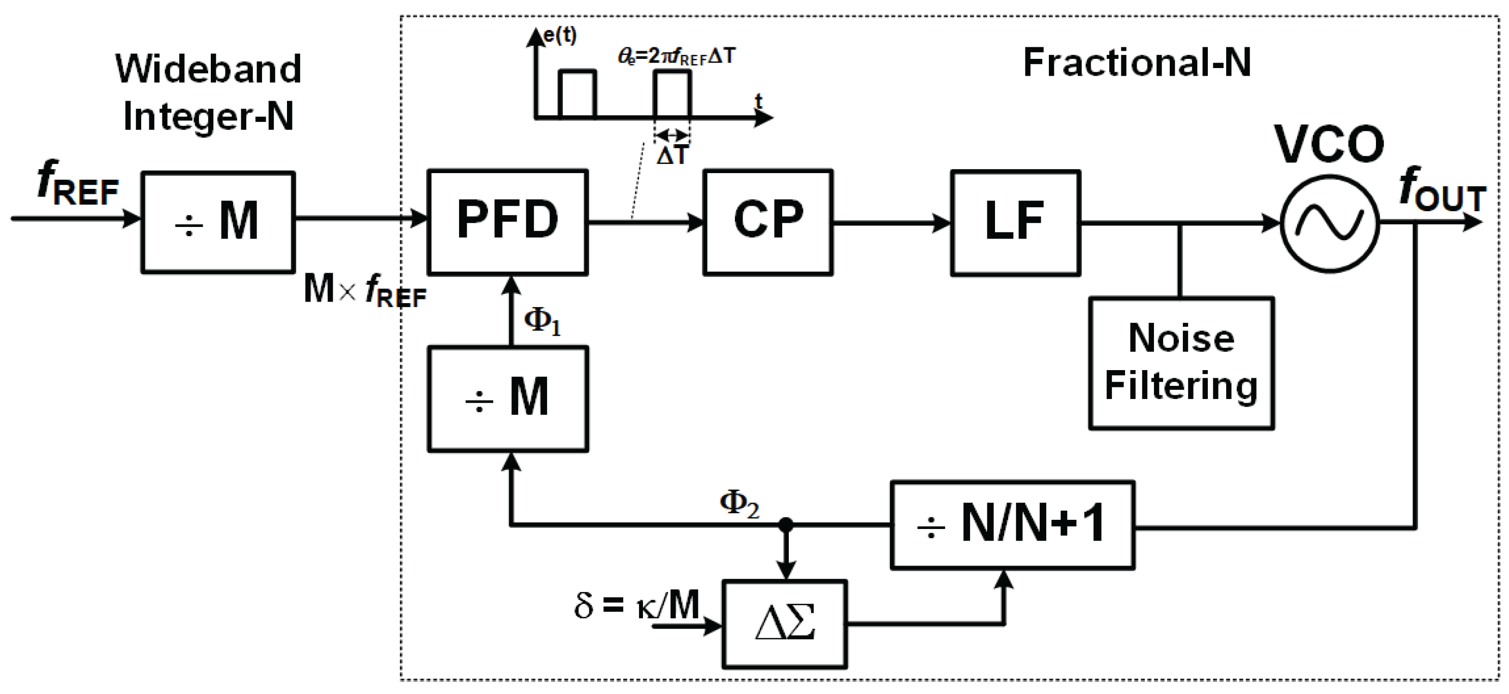
Figure 2.
Timing diagram with N = 4, M= 5 and = 0.2.
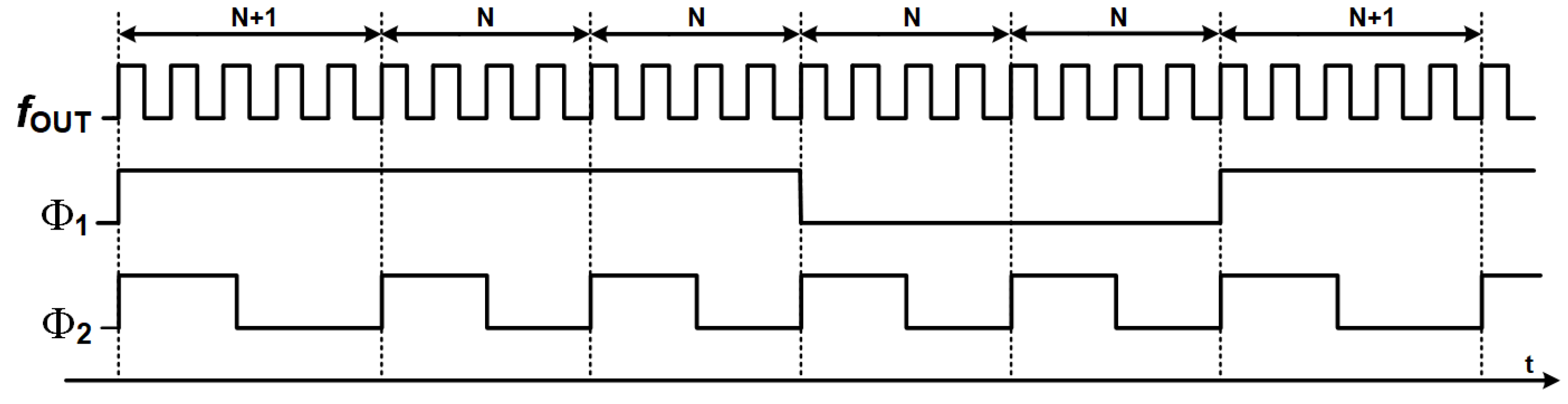
Figure 3.
Dual mode switching PLL.
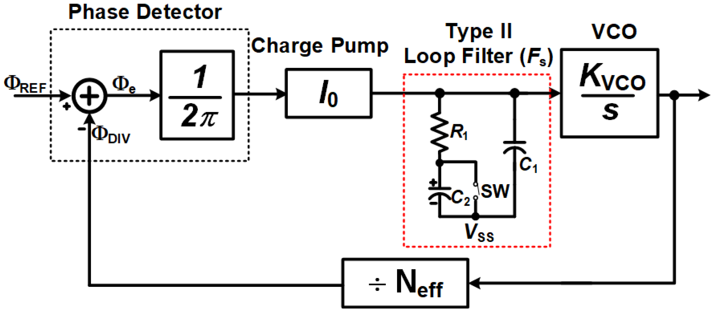
Figure 4.
Hypothetical evolution of phase error with time .
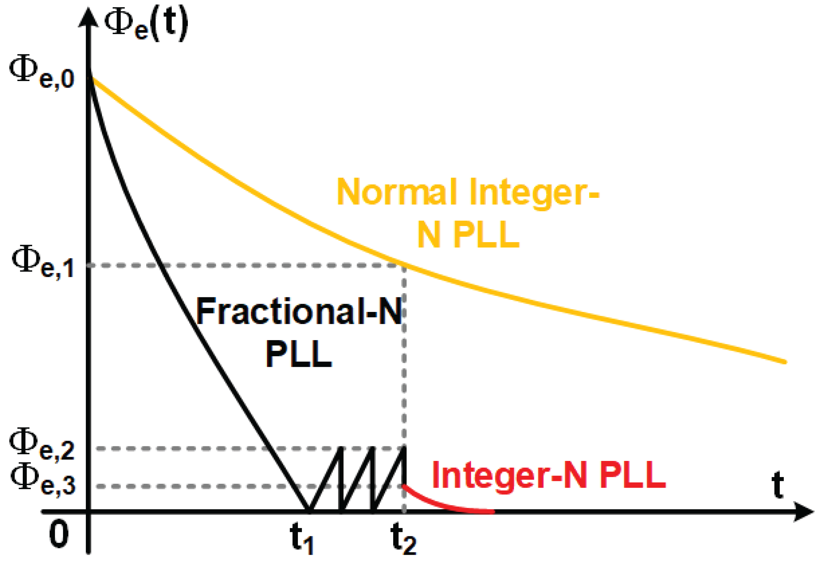
Figure 5.
Bode plots of the magnitude and phase of the open loop transfer function.
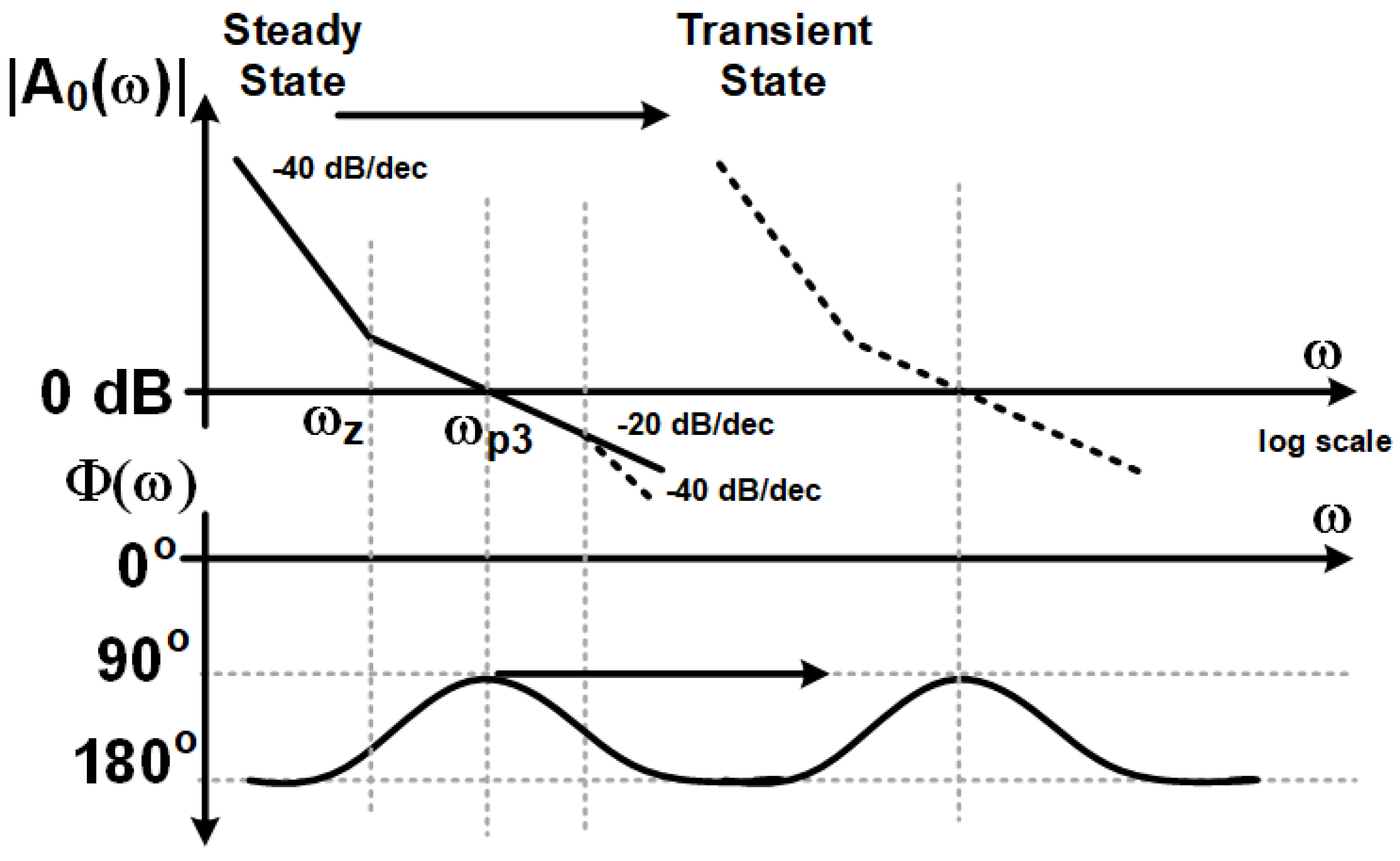
Figure 6.
quantization noise suppression 3-order.
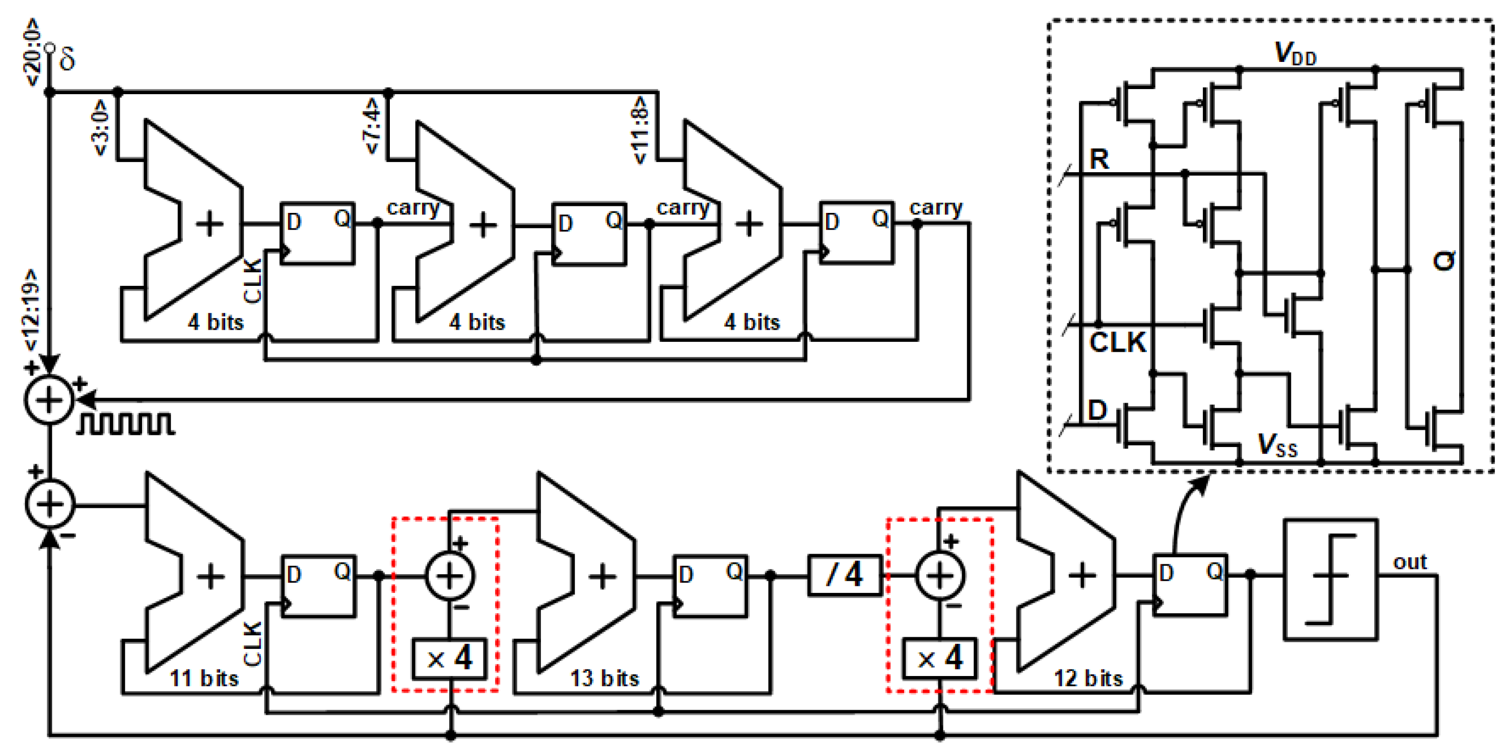
Figure 7.
quantization noise suppression (a) FOM (b) SNR/SNDR versus input amplitude plots.
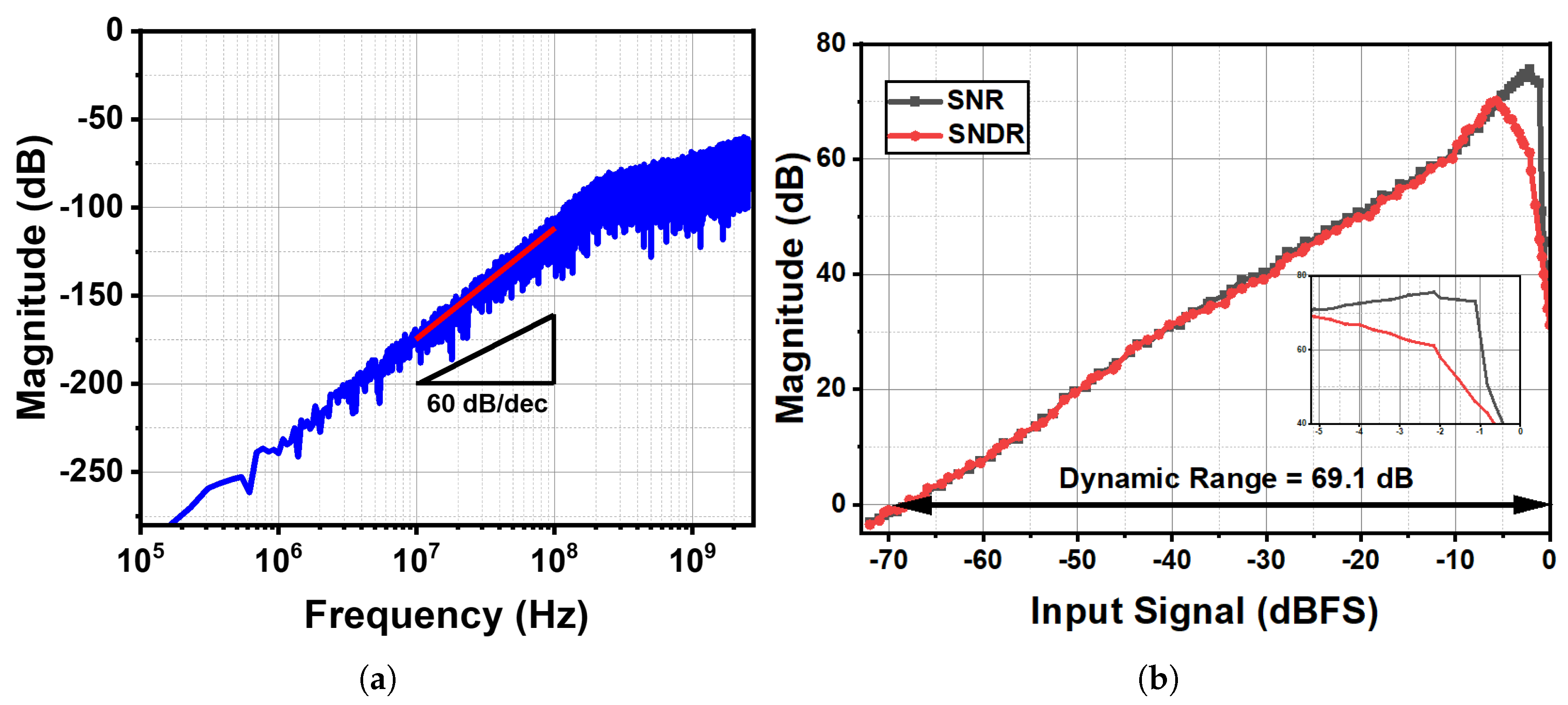
Figure 8.
Noise Filtering Architecture.
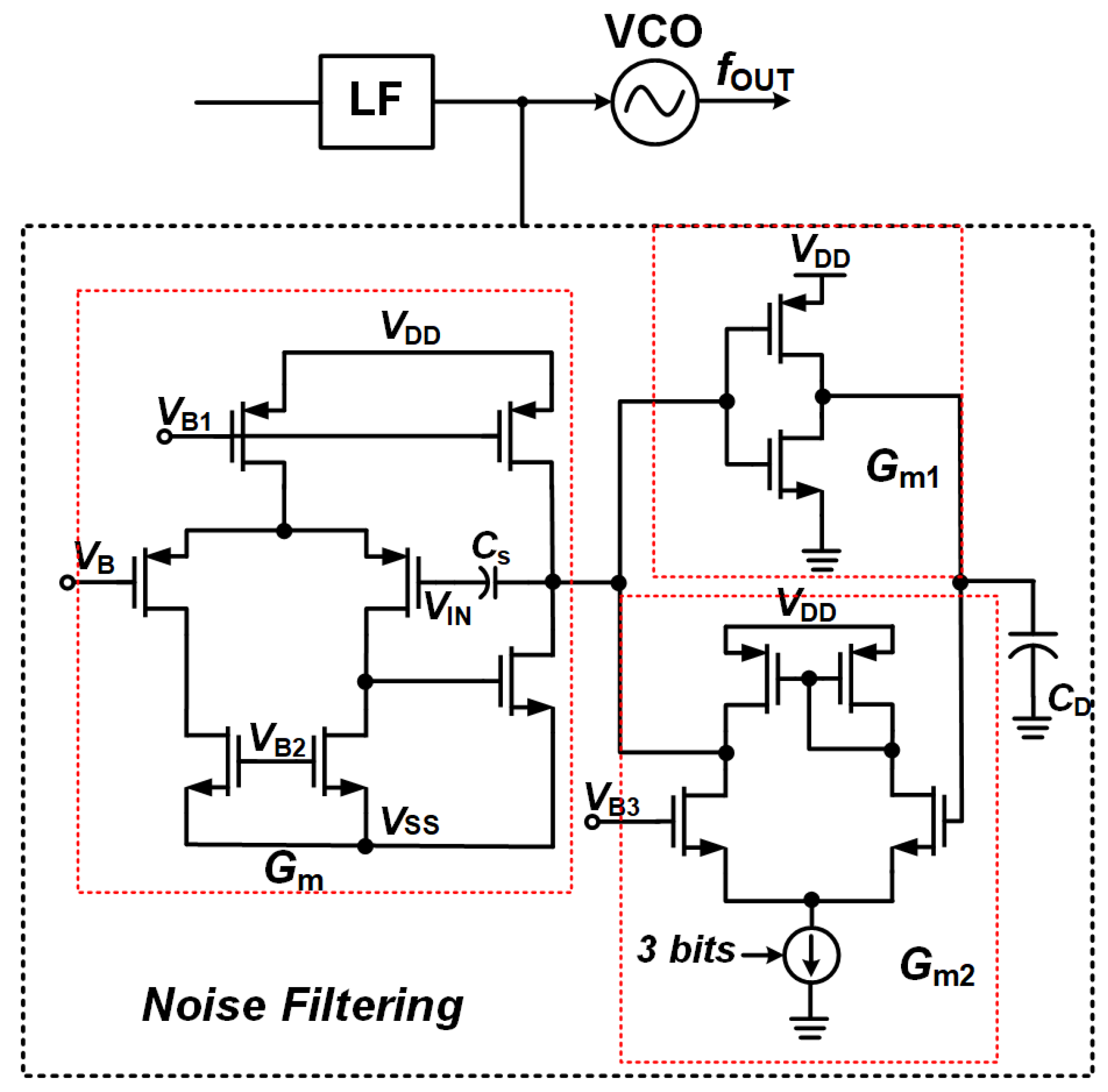
Figure 9.
Integrated noise contribution versus Fractional-N PLL reference frequency.
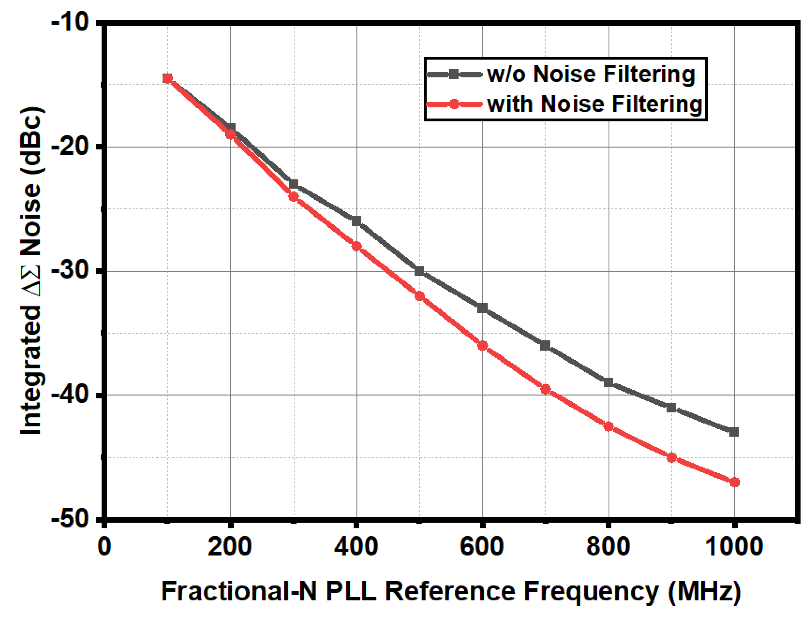
Figure 10.
Proposed Phase Detector.
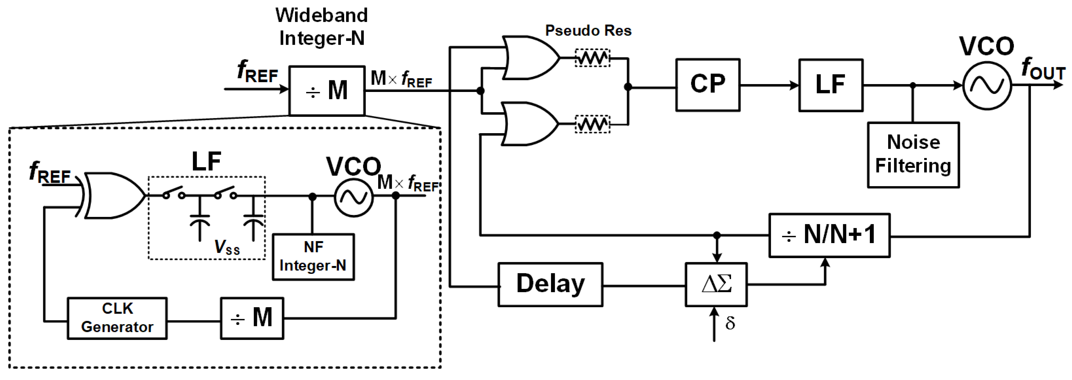
Figure 11.
Proposed VCO circuit block diagram.
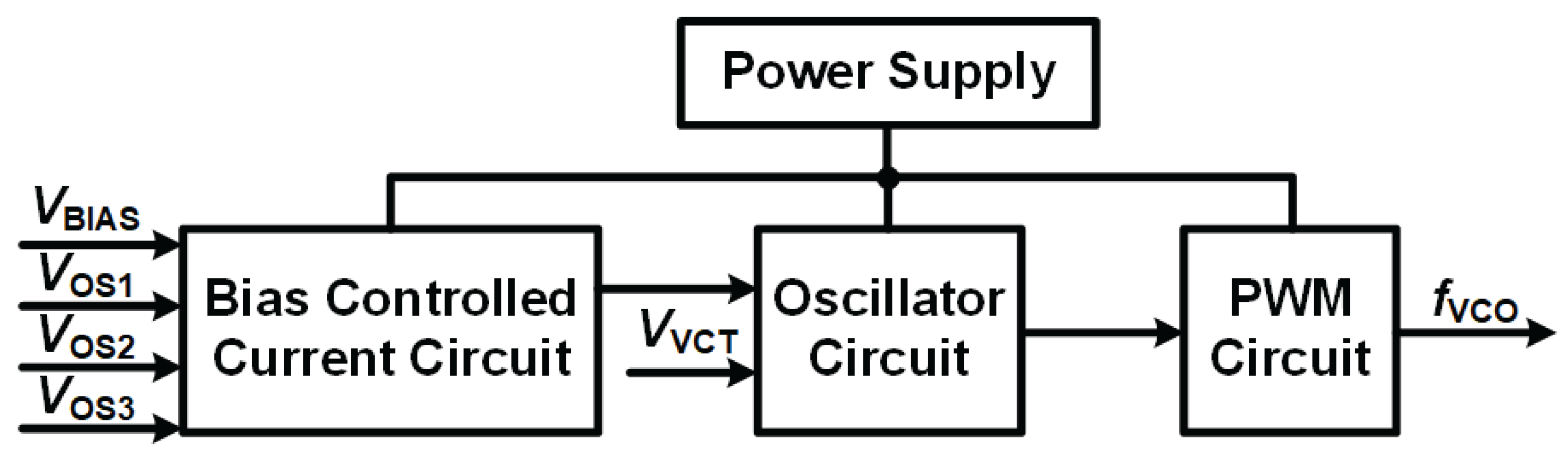
Figure 12.
The three-stage ring oscillator in PLL.
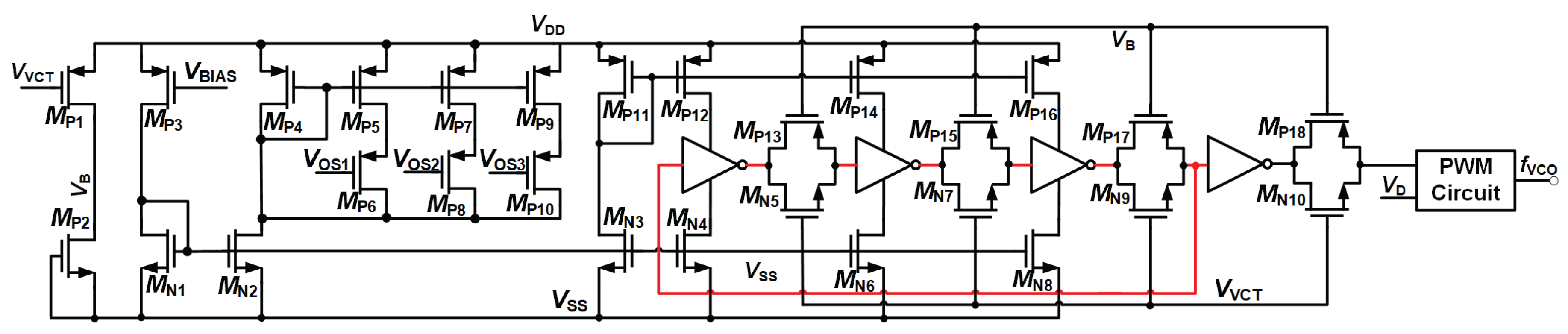
Figure 13.
Simulation proposed VCO (a) Phase noise @ 1 MHz (b) frequency variation with voltage control.
Figure 13.
Simulation proposed VCO (a) Phase noise @ 1 MHz (b) frequency variation with voltage control.
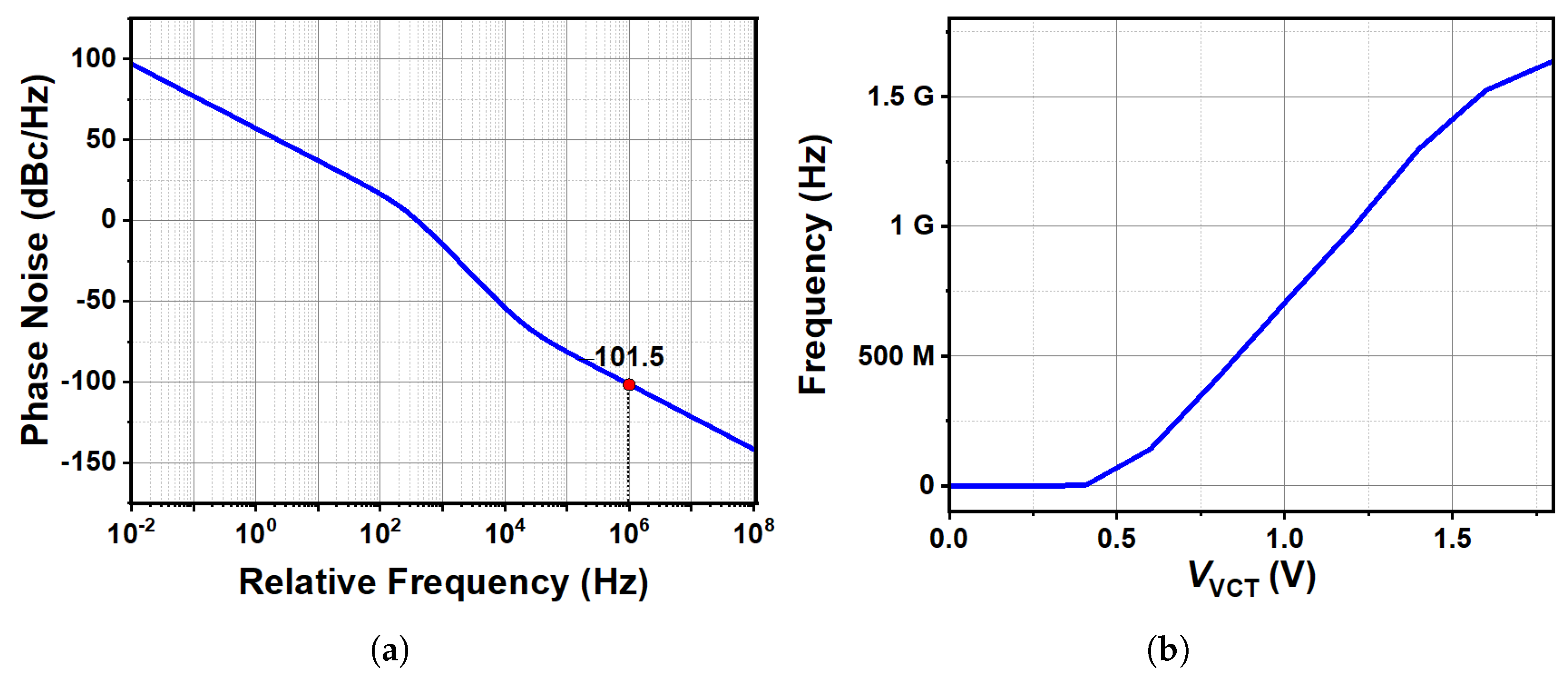
Figure 14.
Die micrograph.
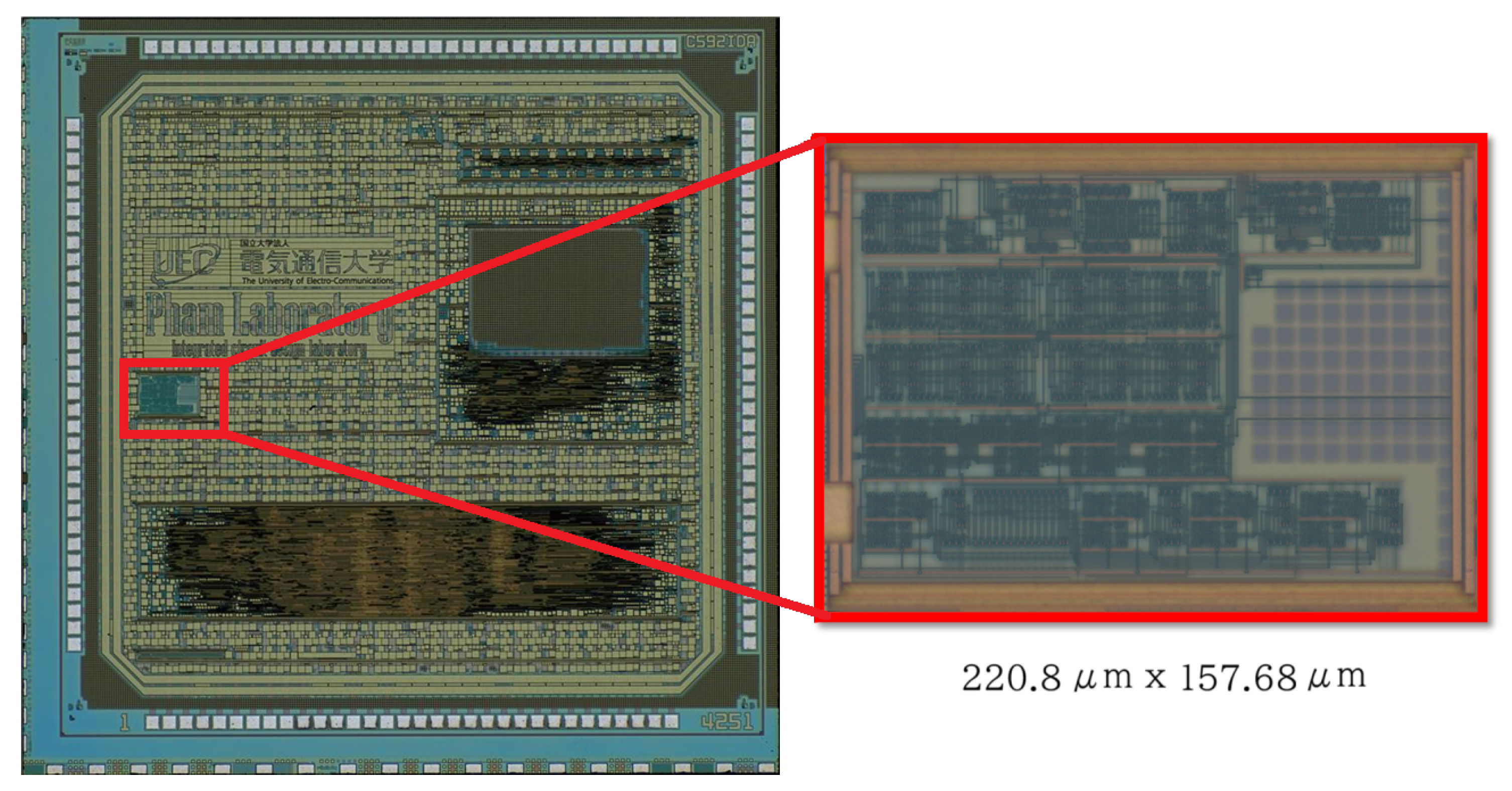
Figure 15.
Largest spur of PLL.

Figure 16.
Reference spur of PLL at 25.5 MHz.
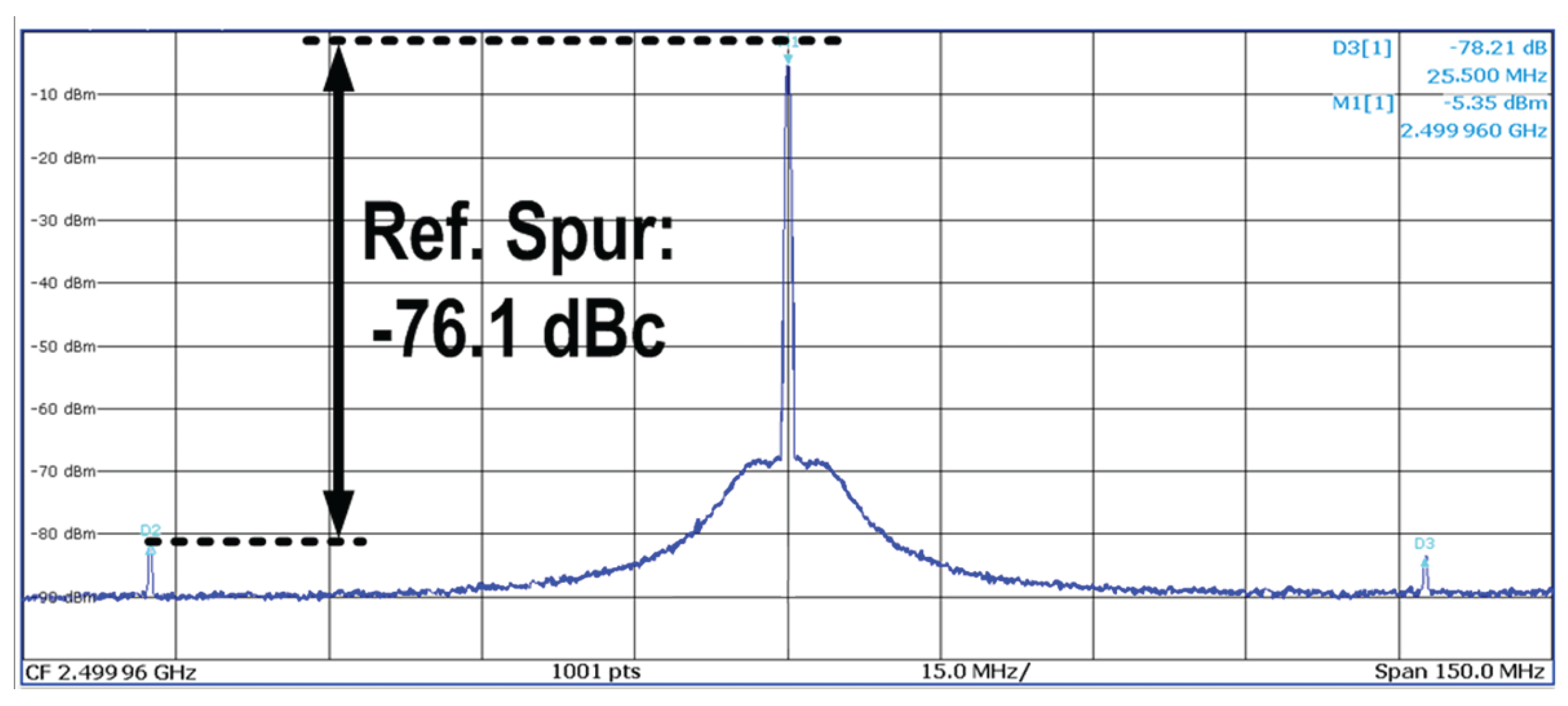
Figure 17.
Phase noise of proposed PLL.
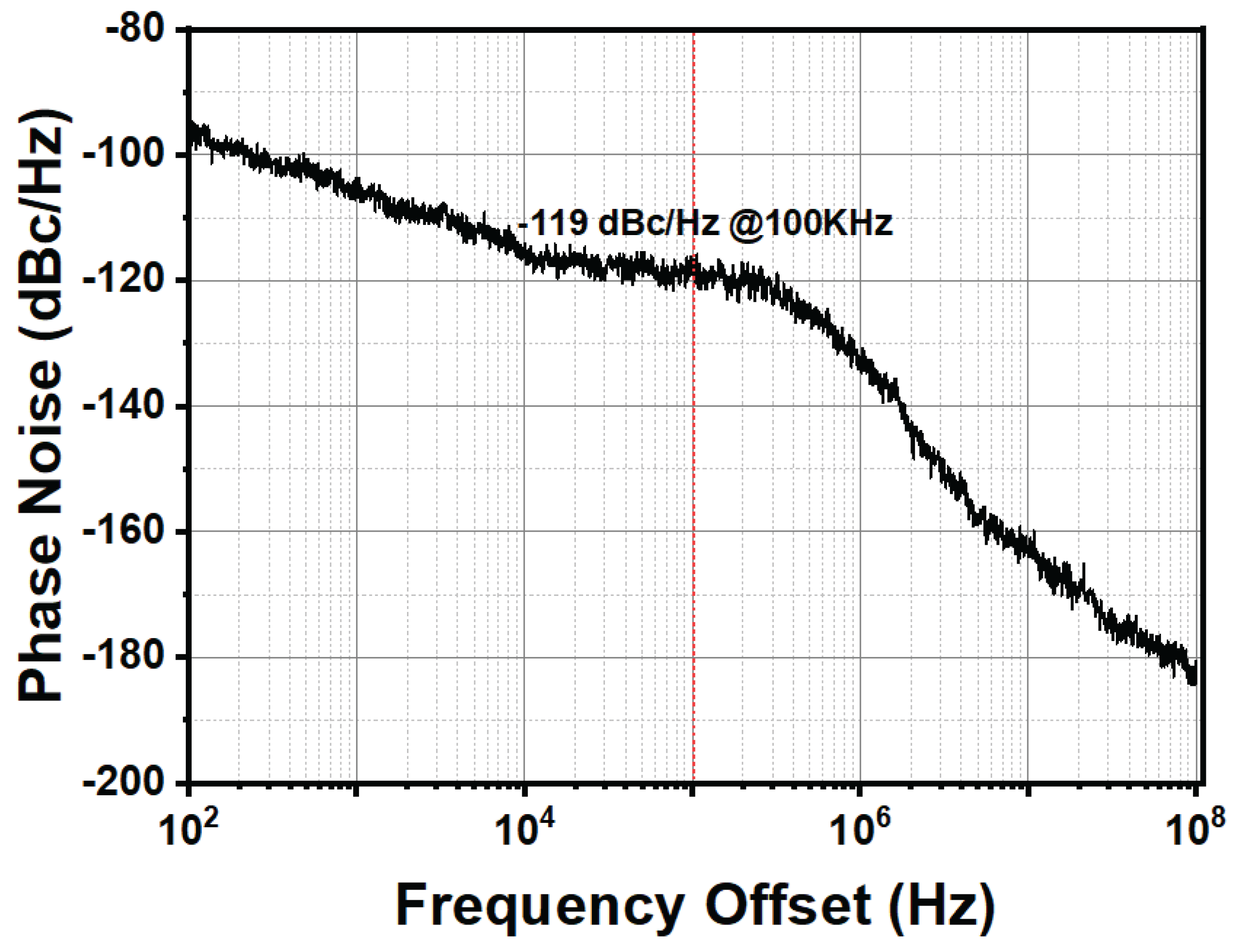

Table 1.
Comparison table.
| This work | [31] | [32] | [33] | [34] | |
| Topology | APLL | APLL | SSPLL | DPLL | MDLL |
| Reference Freq. (MHz) | 25.5 | 26 | 153.6 | 64 | 50 |
| Freq. Range (GHz) | 2.9 ∼3.2 | 1.87 ∼1.98 | 1.9 ∼6.1 | 1.8 ∼2.7 | 1.5 |
| Phase noise @ 100KHz (dBc/Hz) | −119 | −98 | −140 | - | −104 |
| Ref. Spur (dBc) | −76.1 | −67 | - | −47 | −43 |
| FOM* (dB) | −232.22 | −219.4 | −153 | −229.1 | −224.8 |
| Power (mW) | 6 | 10 | 10.1 | 2.76 | 11.95 |
| Area (mm2) | 0.007 | 0.047 | 0.055 | 0.063 | 0.077 |
| Tech. (nm) | 180 | 45 | 28 | 40 | 65 |
Scaled to 28 nm process following [35]
Disclaimer/Publisher’s Note: The statements, opinions and data contained in all publications are solely those of the individual author(s) and contributor(s) and not of MDPI and/or the editor(s). MDPI and/or the editor(s) disclaim responsibility for any injury to people or property resulting from any ideas, methods, instructions or products referred to in the content. |
© 2025 by the authors. Licensee MDPI, Basel, Switzerland. This article is an open access article distributed under the terms and conditions of the Creative Commons Attribution (CC BY) license (http://creativecommons.org/licenses/by/4.0/).
Copyright: This open access article is published under a Creative Commons CC BY 4.0 license, which permit the free download, distribution, and reuse, provided that the author and preprint are cited in any reuse.


