Submitted:
13 January 2025
Posted:
14 January 2025
You are already at the latest version
Abstract
We perform a theoretical investigation of the electron-surface optical phonon (SOP) interaction in van der Waals heterostructures (vdWHs) formed by monolayer graphene (1LG) and transition metal dichalcogenides (TMDCs), using eigenenergies obtained from the tight-binding Hamiltonian for electrons. Our analysis reveals that the SOP interaction strength strongly depends on the specific TMDC material. TMDC layers generate localized SOP modes near the 1LG/TMDC interface, serving as effective scattering centers for graphene carriers through long-range Fröhlich coupling. This interaction leads to resonant coupling between electronic sub-levels and surface phonon modes, causing Rabi splitting of the electron energy levels. We further explore the influence of different TMDCs, such as WS₂, WSe₂, MoS₂, and MoSe₂, on transport properties such as SO phonon-limited mobility, resistivity, conductivity, and scattering rates across various temperatures and charge carrier densities. Our analysis confirms that at elevated temperatures and low carrier densities, surface optical phonon scattering becomes a dominant factor in determining resistivity. Additionally, we investigate the Auger recombination process at the 1LG/TMDC interface, showing that both Auger and SO phonon scattering rates increase significantly at room and higher temperatures, ultimately converging to constant values as the temperature rises. In contrast, their impact is minimal at lower temperatures. These results highlight the potential of 1LG/TMDC-based vdWHs for controlling key processes, such as SOP interactions and Auger recombination, paving the way for high-performance nanoelectronic and optoelectronic devices.
Keywords:
Graphene
; Transition metal dichalcogenides
; Surface Optical Phonon Scattering Rate
; Van der Waals Heterostructures
; Auger Scattering Rate
; WS2
; WSe2
; MoS2
; MoSe2
1. Introduction
Graphene, a two-dimensional material just a few atoms thick, has attracted global interest for its potential in developing next-generation miniaturized and smart electronic devices [1]. However, its lack of a band gap poses challenges, particularly for semiconductor applications [2]. To overcome this limitation, considerable research has focused on methods to induce a band gap in graphene, notably through the creation of van der Waals (vdW) heterostructures [3]. These heterostructures, composed of graphene and transition metal dichalcogenides (TMDCs), leverage the exceptional electronic characteristics of both materials, offering significant advancements in semiconductor device technology [4,5]. The combination of these two-dimensional (2D) materials has attracted considerable attention due to their potential use in ultrathin, flexible, and transparent electronic and optoelectronic applications [6]. By integrating the optical and photoelectric properties of various materials, vdW heterostructures combine the benefits of direct gap semiconductors with strong electron–phonon coupling and high mobility characteristics typical of semimetals [7,8,9,10]. For instance, when graphene is layered atop a single TMDC layer, it can modify graphene’s intrinsic electronic properties while preserving its Dirac cone structure [11].
Graphene-TMDC heterojunctions, which exhibit strong electron–phonon coupling, are promising for nano-photodetectors [12]. However, chemical doping can negatively affect graphene’s performance, and limitations in photoelectric conversion and the regulation of interlayer interactions pose obstacles for further research on these heterostructures. Interfacial interactions can modify graphene’s electronic properties, as shown by the appearance of satellite Dirac cones when graphene is placed on hexagonal boron nitride substrates. Current research aims to investigate interfacial interactions with various materials to tailor specific electronic properties [13,14,15,16,17,18,19].
Among the studies on 2D/2D van der Waals heterostructures (vdWHs), the combination of graphene, known for its high carrier mobility, and transition metal dichalcogenides (TMDCs) with semiconducting properties, particularly graphene/MoS2 (Gr/ MoS2), stands out as a promising candidate for various applications. These include electronics [20,21], energy storage [22,23], gas sensors [24,25], and chemical sensors [26,27]. The synergy between graphene’s high mobility and the unique properties of TMDCs enables enhanced performance across these fields.
Two-dimensional (2D) tungsten disulfide (WS2) has also gained considerable attention for optoelectronic applications due to its direct bandgap, high carrier mobility, chemical stability, and strong light-matter interactions. The complementary properties of van der Waals (vdW) heterostructures formed by 2D WS2 and graphene, offer promising potential for excitonic optoelectronic performance. However, the strong recombination of excitons in WS2 poses a significant challenge in achieving a highly sensitive photodetector [12].
Recently, many graphene-based vdW heterostructures have been investigated theoretically and experimentally [28]. However, most studies on graphene heterojunctions have mainly focused on their electronic structures [29], preparation methods [30], and applications [31], with limited research on their electron transport properties and intrinsic mechanisms. To advance the practical use of graphene heterojunctions in nanoelectronic devices, it is crucial to develop new heterojunctions and investigate their electron transport characteristics. Monolayer WS2 with its excellent electron mobility and substantial direct bandgap, also holds significant potential for various nanodevice applications [12,32].
In Van der Waals heterostructures composed of graphene and 2D transition metal dichalcogenides (TMDCs), electron interactions with surface optical (SO) phonons are a key factor influencing electronic properties, such as carrier mobility and scattering rates. When graphene is combined with TMDC layers like MoS2 or WSe2, the lattice mismatch and the high dielectric environment contribute to enhance electron-SO phonon coupling. Studies have shown that SO phonons, particularly in polar substrates, can strongly couple with carriers in adjacent 2D layers, creating a distinct energy dispersion that affects the electronic band structure [13,14,15,16,17,18,19]. This coupling is especially notable in heterostructures on polar substrates such as silicon carbide (SiC) or hexagonal boron nitride (hBN), which facilitate resonant interactions at specific phonon frequencies [13,14,15,16,17,18,19]. By tuning these interactions, researchers aim to optimize device performance in applications ranging from high-speed transistors to optoelectronic components, where carrier dynamics and scattering mechanisms are critical. Recent theoretical and experimental investigations provide insights into how SO phonon modes can be modulated by the material composition and interlayer distance, offering a pathway to finely control electronic behavior in graphene-TMDC heterostructures [33].
For example, in their study, J. Zhen et al. [34] focused on the high carrier mobility and strong electron-phonon coupling in graphene-WS2 heterostructures under hydrostatic pressure. The authors explored how pressure influences charge transfer, Fano resonance, and band structure within these heterostructures using density functional theory (DFT) calculations. The research suggests that graphene-TMD (transition metal dichalcogenide) heterostructures exhibit promising potential for optoelectronic applications due to these unique electronic properties [35].
Theoretical models also provide critical insights, predicting electron relaxation and many-body effects induced by SO phonons in graphene placed on polar substrates, such as SiC or hBN. These models often use the self-energy framework to explain how energy dissipation occurs due to SO phonon emission, particularly at high electric fields. Calculations show that in systems like graphene-SiC, the interaction can significantly modify carrier dynamics, including the lifetime and spectral properties of quasiparticles, where electron-SO phonon interactions produce a distinct energy gap, limiting certain energy transitions. This theoretical perspective helps explain experimental findings related to electron transport and thermal dissipation observed in these heterostructures [13,14,15,16,17,18,19].
In combining these findings, both theoretical predictions and experimental validations illustrate how SO phonons can alter the electronic and optical properties of vdW heterostructures. Such interactions are crucial for developing future nanoelectronic and photonic devices that rely on controlled phonon interactions within 2D materials.
Recent studies, both experimental and theoretical, have explored electron-surface optical phonon interactions in van der Waals (vdW) heterostructures made from graphene and transition metal dichalcogenides (TMDCs), particularly to understand their impact on optoelectronic properties. The interaction between electrons and surface optical phonons within these heterostructures can significantly influence charge and energy transfer, as well as the relaxation dynamics of excitons, which are essential for applications in photodetectors, light-emitting devices, and other nanophotonic systems [12].
In experimental research, charge transfer and exciton-phonon coupling in graphene-TMDC heterostructures have been closely analyzed using photoluminescence and Raman spectroscopy. For instance, studies presented by Guillaume et al. have shown that when graphene is combined with a TMDC layer like MoS2 or MoSe2, interlayer electron transfer occurs rapidly, reducing photoluminescence and modifying exciton lifetime, which is primarily driven by strong exciton-phonon coupling in these vdW interfaces [34].
On the theoretical side, modeling efforts have focused on simulating how phonon polaritons quasiparticles formed from coupling between photons and phonons in polar materials behave in vdW structures, often incorporating materials such as hexagonal boron nitride (hBN) that introduce unique hyperbolic phonon polariton modes. These modes offer potential for high optical confinement and controlled light-matter interactions at the nanoscale, which are beneficial for device miniaturization and enhanced energy transfer [35].
Overall, these advances underscore the crucial role of electron-surface optical phonon interactions in tailoring the optoelectronic responses of vdW heterostructures, facilitating their application in next-generation electronic and photonic devices.
Recent advancements in graphene-TMDC heterostructures highlight their potential in high-mobility field-effect transistors (FETs), sensors, and modulators. These heterostructures combine graphene’s exceptional conductivity and carrier mobility with the semiconducting and optoelectronic properties of TMDCs, such as MoS2 and WSe2. Graphene acts as a highly conductive channel, while TMDC layers modulate charge transport through their tunable bandgaps. This synergy has been demonstrated to enhance the performance of FETs, achieving mobilities exceeding 8,000 cm²/Vs, suitable for next-generation high-speed electronics and optoelectronics. Additionally, the heterostructures’ strong light absorption and efficient charge transfer mechanisms enable sensitive photodetection and precise light modulation, making them ideal for optical sensors and modulators [36,37].
In this paper, we present an overview of our theoretical studies of one specific dynamical optical property, namely electron-phonon (e-ph) interactions in single layer graphene-TMDC heterostructures. This material exhibits a high electronic quality, in which charge carriers can travel thousands of interatomic distances without scattering [37,38]. These interactions between the electronic excitations and phonons are responsible for the formation of polarons in the single layer graphene-TMDC heterostructures. The Auger process in graphene-based heterostructures with transition metal dichalcogenides (TMDs) like WS2, WSe2, MoS2, and MoSe2 involves the interaction of charge carriers that leads to non-radiative recombination. In these heterostructures, the proximity of graphene to TMDCs enhances carrier dynamics, with energy transfer processes such as interlayer charge transfer playing a significant role [40,41].
In graphene/TMDCs systems, the strong interlayer coupling can enable Auger recombination, which involves the transfer of energy from one carrier to another within the TMDC layer. This process is influenced by defect states and can be observed through phenomena like photoluminescence quenching under specific temperature conditions [40,41].
These heterostructures provide tunable electronic and optical properties through external factors like electric fields, enabling control over processes such as charge transfer and Auger recombination, which are vital for optimizing device performance in nanoelectronics and photodetectors [40,41].
This paper is organized as follows; first, we investigate the electrical transport in graphene-TMDC heterostructures by calculating the SO phonon-limited mobility, the SO phonon-limited conductivity, the SO phonon-limited resistivity and the scattering rate in single layer graphene-TMDC (1LG/TMDC) heterostructures. Second, we study theoretically the electron-surface phonon interaction in 1LG/TMDC heterostructures. Finally, we investigate the Auger recombination process in the 1LG/TMDC interface.
2. The Electrical Transport in 1LG/ TMDC Interface
In this section, we investigate the effects of various TMDCs on the SO phonon-limited mobility, conductivity, resistivity, and scattering rate in single-layer graphene-TMDC heterostructures. This analysis considers the influence of SO optical phonon scattering originating from the TMDCs and examines how these properties change with temperature.
In recent years, research on electron mobility within Van der Waals heterostructures composed of graphene and 2D transition metal dichalcogenides (TMDCs) (see Figure 1) has expanded significantly. These heterostructures exhibit promising electrical transport properties, influenced largely by the interactions at the graphene-TMDC interface. Electron mobility in these systems is notably high due to graphene’s intrinsic high conductivity, yet it is modified by coupling with the TMDC layer. For example, in graphene/WS2 heterostructures, theoretical studies show that electron mobility is enhanced due to the weak interlayer interactions that preserve the Dirac cone structure of graphene while benefiting from the TMDC’s strong spin-orbit coupling properties. Such interactions are pivotal for achieving linear current-voltage characteristics, as noted in heterostructure studies utilizing density functional theory and other advanced simulations [12,33].
Experimentally, electron mobility is also highly dependent on the choice of TMDC material and the fabrication quality of the heterostructure. Variations in stacking angles and interlayer distance can significantly impact heterostructure electron mobility, as they influence the degree of charge transfer and scattering effects at the interface. For instance, research on MoS2/graphene heterostructures demonstrates that optimal stacking and minimal interfacial defects allow for a balance between high mobility and controlled charge transfer, thus making these structures suitable for high-performance electronic applications [42].
These findings underscore the potential of graphene-TMDC heterostructures in applications requiring both high electron mobility and tunable electronic properties, such as next-generation photodetectors and flexible electronic devices [12].
Graphene exhibits remarkable electronic properties, particularly its exceptionally high mobility. This characteristic primarily stems from the reduced number of scattering centers in graphene, thanks to the strong covalent chemical bonds that contribute to its extraordinary rigidity. These bonds result in a crystal structure with very few defects, which are typically a major source of electronic scattering in most materials. It’s important to note that mobility is closely tied to a material’s electrical conductivity and the level of impurities it contains. Higher mobility means that electrons can travel further without colliding with impurities or crystal defects. Additionally, graphene’s high mobility is also intrinsically linked to the unique nature of its electrons, which, unlike those in most materials, behave as particles with zero effective mass.
The low field mobility μ can be determined by solving the Boltzmann transport equation in the stationary regime, expressed as: where is the electrical conductivity, is the carrier density, is the density of states, is the Fermi energy, and is the scattering time. The latter can be evaluated using the method described in Reference [43]:
(1)
Here is the Bose-Einstein phonon occupation number, is a directional angle of wave vector k. Where is given as follows:
(2)
Here represents the van der Waals distance between the 1LG and TMDC.
Figure 2 illustrates the SO phonon-limited mobility as a function of temperature in monolayer graphene-TMDC heterostructures (1LG/TMDCs). As depicted in Figure 2, the SO phonon-limited mobility decreases as the temperature increases depending on the specific type of TMDC (see Table 1).
Figure 3 shows SO phonon-limited resistivity versus the temperature in 1LG/TMDCs interfaces. As shown in Figure 3, the SO phonon-limited resistivity is enhanced by the increasing of the temperature. In general, thermal energy causes vibration of carbon, resulting in the increase of the SO phonon-limited resistivity, thus limiting the maximum conductivity therein. The resistivity can be reduced only by strong cooling of the material.
Figure 4 illustrates the SO phonon-limited conductivity as a function of charge carrier density in a 1LG/TMDC interface at a temperature of 300 K. As the charge carrier density increases, the SO phonon-limited conductivity becomes more significant, leading to a corresponding decrease in the SO phonon-limited resistivity, given by . Similarly, Figure 5 shows the temperature dependence of the scattering rate in 1LG/TMDC interface for a charge carrier density of . These results indicate that at room temperature and above, the SO phonon scattering rate increases notably, while its impact is minimal at low temperatures. Moreover, at elevated temperatures and low carrier densities, surface optical phonon scattering becomes a dominant factor in determining the resistivity [13,14,15,16,43].
The SO phonon modes at the 1LG/TMDC interface generate a long-range electric field that impacts the electrons in the graphene sheet, typically located around 4 Å away. Remote phonon scattering and its influence on carrier mobility in two-dimensional electron systems are well-established phenomena in semiconductor physics, having been studied in quantum wells and other heterostructures, including metal-oxide-semiconductor field-effect transistors [44]. This effect is more pronounced in graphene due to the significantly smaller vertical dimensions of the devices, governed by the van der Waals distance.
Graphene’s atomically thin structure makes its transport properties highly sensitive to the choice of the surrounding TMDC. Ideally, TMDCs should have both high static dielectric constants and high phonon energies that are not activated during low-field transport. This combination could pave the way for achieving ballistic transport in graphene. In particular, TMDCs, with high dielectric constants and high SO phonon energies, would be the most desirable for future applications. As illustrated in Figure 5 for the 1LG/TMDC interface, high-temperature transport in graphene is likely dominated by SO phonon scattering from the TMDCs.
3. Electron-Surface Optical Phonon Interaction in 1LG/TMDC Interface
In graphene, the honeycomb lattice does not qualify as a Bravais lattice because the A and B atomic positions are distinct and inequivalent. However, if considered independently, the A (or B) atomic positions form a hexagonal Bravais lattice, often referred to as the ’A sublattice’ (or ’B sublattice’). This configuration can also be described as a triangular lattice with a basis consisting of two atoms per unit cell (refer to Figure 6). The primitive vectors defining the honeycomb lattice are as follows:
; The symbol represents the carbon-carbon bond length, approximately . The reciprocal lattice is defined by the following lattice vectors:
; The two points K and K’ at the corners of the graphene Brillouin zone (BZ) have a particular importance for the physics of graphene. Their positions in momentum space are given by:
;
In our theoretical study, we employed the tight-binding Hamiltonian for electrons at the 1LG/TMDC interface, assuming that electrons can hop to both nearest and next-nearest neighbor atoms. The Hamiltonian has the following form [45]:
(3)
Here, “H.c.” refers to the “Hermitian conjugate,” and represents the nearest-neighbor hopping energy (the hopping between different sublattices) [45]. The energy bands derived from this Hamiltonian are provided as follows [45]:
(4)
where
(5)
(6)
In this study, we explore the interaction between electrons and surface optical phonons (SOP) at the 1LG/TMDC interface, focusing on the long-range Fröhlich coupling. This model offers a solid framework for understanding electron-SOP interactions at the 1LG/TMDC interface, but it relies on several assumptions. For instance, it typically applies the Born-Oppenheimer approximation [46]. Short-range interactions, such as electron-phonon interactions in graphene [47], are excluded, and nonlinear interactions and multi-phonon processes are generally neglected [48]. The Fröhlich model also omits the effects of impurities, defects, and other types of disorder that can influence electron-phonon interactions in real materials [46,49]. Additionally, the phonon dispersion is usually assumed to be linear, an approximation that may not apply to all phonon modes or substrates [50]. Often, only a single dominant phonon mode is considered, overlooking the potential contributions from multiple phonon modes [47].
To simplify our analysis, we assume an isotropic phonon spectrum, meaning that phonons are either longitudinal or transverse in polarization. The Fröhlich Hamiltonian includes an interaction term in which an electron scatters from to , involving the emission or absorption of a phonon. In both cases, the conservation of total momentum is maintained, and it is expressed as follows:
(7)
The term represents the phonon energies, which include both the Longitudinal Optical (LO) and Surface Optical (SO) modes, and can be written as:
(8)
In this context, , denote the creation and annihilation operators, respectively, for the phonon with wave vector , while refers to the frequency of the phonon.
The second term, is the Hamiltonian describing the interaction between the electron and phonon [51]:
(9)
The Fröhlich Hamiltonian is expressed as follow:
(10)
The interaction between electron in monolayer graphene and TMDC-surface optical phonon in the interface 1LG/TMDCs heterostructure is described by the second term in Equation (10).
Where denotes the coupling element in the Fröhlich Hamiltonian and describing the interaction between the electron in monolayer graphene and surface optical phonon of the TMDCs. This matrix element is given by [52,53,54]:
(11)
In the given context, describes the magnitude of the polarization field, which is determined by the Fröhlich coupling [55]:
(12)
Here, and are the low- and high-frequency dielectric constants of the TMDCs, (see Table 1), refers to the internal distance between the 1LG and TMDC. The term denotes the energy of SO phonon of the polar substrates with two branches
The surface optical phonon (SOP) energies are derived from the bulk longitudinal optical (LO) phonons as follows [63]:
(13)
The screening of the Coulomb interaction by the TMDC dielectric environment is considered through. Given the weak screening of the electric field perpendicular to the plane of the TMDCs, is set to 1 [64].
In the 1LG/TMDC interface, the surface optical phonons (SOP) induce an electric field that interacts with the electrons in the neighboring monolayer graphene. Using equations (11) and (12), the SOP coupling is expressed as follows:
(14)
The summation is carried out over one spin and one valley, where represents the area of the two-atom unit cell.
In this analysis, we have followed the same theoretical approach used in our previous calculations [13,14,15,16,17,18,19]. To investigate the interactions between electrons and surface optical phonons in monolayer TMDCs, we have specifically considered the electronic states.
and ,with electron energies and ,respectively.
The space of polaronic states is obtained from the tensor product of the electronic and phononic state spaces. Therefore, we define new states, referred to as polaronic states, given by:
(15)
(16)
Figure 7 depicts the strength of the surface optical (SO) coupling between the electronic states and versus the wave vector in 1LG/TMDC interface. As shown in Figure 7, it is clear that the coupling with surface optical phonons (SOP) is strongly affected by the type of TMDCs.
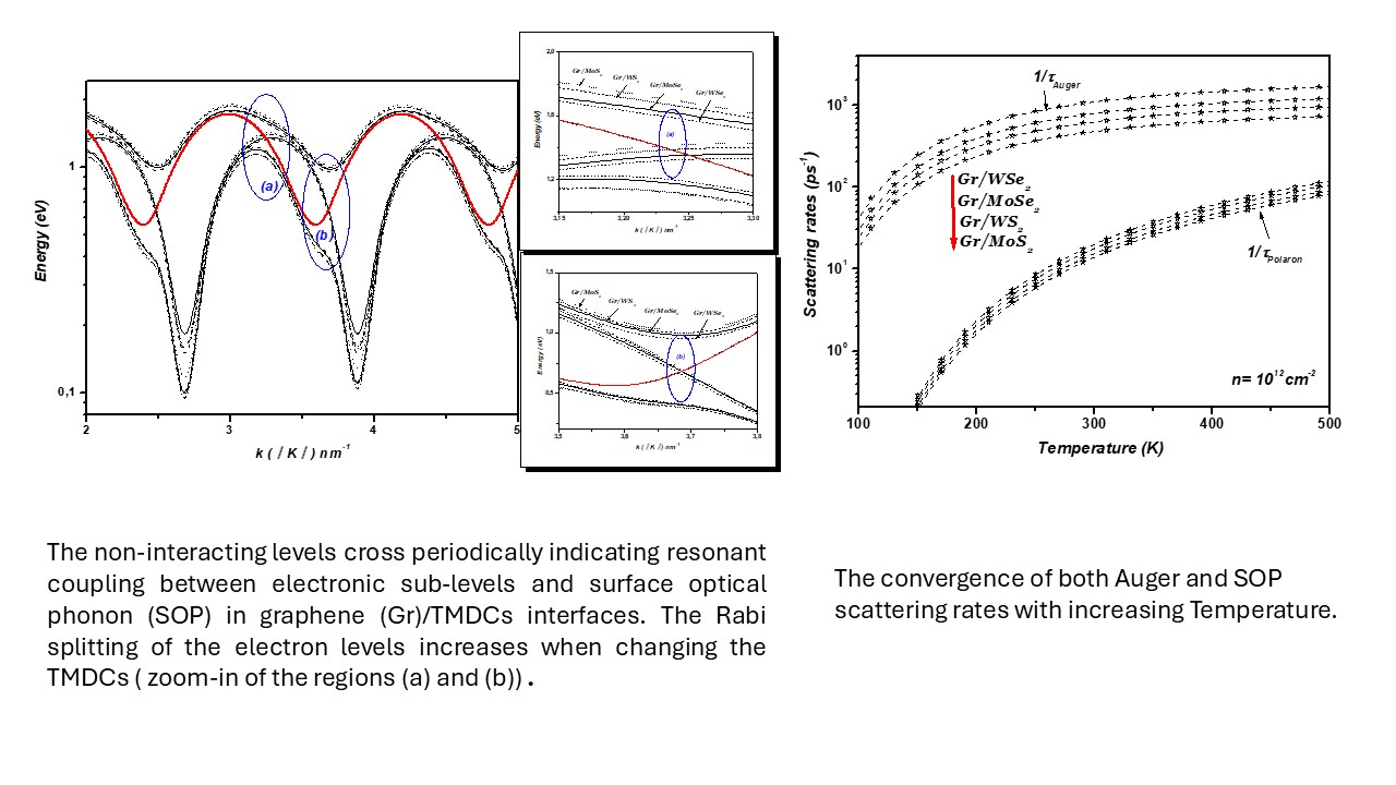
Figure 8 (a, b, c, d) display the polaron electron energies as a function of the wave vector , with varying along the Γ-K direction in monolayer graphene-TMDC heterostructures. For comparison, the energies of the non-interacting states are also plotted in the same figures and . These noninteracting levels cross periodically near and (n is an integer) indicating resonant couplings (see Figure 8 and Figure 9). These crossings imply that the energy separations between the electronic levels are equal to , , and for the MoS₂ WS₂, MoSe₂ and WSe₂ respectively. They are replaced by large anticrossings energy levels around (~490meV; ~ 620meV), (~460meV; ~600meV), (~451meV; ~590meV) and (~429meV ; ~569meV) respectively. It can be seen in Figure 8 that the Rabi splitting of the electron levels increases when changing the TMDCs (MoS₂ WS₂, MoSe₂ and WSe₂) in mono-layer graphene-TMDCs interfaces.
In these anticrossings, the wave functions of the levels become mixed, enabling multiple transitions such as: such as: and . This indicates that the interaction between electrons and surface optical phonons (SOP) cannot be regarded as weak coupling. The coupling between electrons and SOP results in the Rabi splitting of the electron levels. Hence, the calculations reveal the possibility of resonant coupling between the electronic sub-levels and surface vibrations in the 1LG/TMDC interface.
4. Auger Recombination in 1LG/TMDCs Interfaces
Auger recombination is a non-radiative process where the recombination energy of an electron-hole pair excites another carrier, playing a vital role in reducing photoluminescence efficiency [65,66]. This mechanism affects the performance of light-emitting devices and photodetectors by governing energy transfer dynamics and enabling carrier multiplication, which can enhance device sensitivity under certain conditions.
The optical properties arising from Auger recombination in 2D materials, especially those involving transition metal dichalcogenides (TMDCs) such as WS₂, WSe₂, MoS₂, and MoSe₂, are significant for their implications in photonics and optoelectronics. Auger recombination is a non-radiative process where energy from an electron-hole recombination is transferred to another carrier, often leading to carrier multiplication or energy dissipation.
To investigate the Auger recombination process in the 1LG/TMDC interface, we have taken advantage of circular symmetry employing the massless Dirac fermion Hamiltonian (MDF), we have used the semiclassical Boltzmann equation with a collision integral that includes the contribution from electron-electron (e-e). This allows us to take particular care of collinear scattering process including Auger recombination (AR).
To investigate the Auger recombination (AR) process at the 1LG/TMDC interface, we employed the massless Dirac fermion (MDF) Hamiltonian, leveraging the circular symmetry of the system. The semiclassical Boltzmann equation was used, with a collision integral that includes the effects of electron-electron (e-e) interactions. This approach allowed us to carefully analyze collinear scattering processes, including AR. The behavior of carriers in graphene was described using the MDF Hamiltonian [67,68,69,70].
The behavior of carriers in graphene is governed by the massless Dirac fermion (MDF) Hamiltonian [67,68,69,70],
,(17)
Here, the field operator annihilates an electron with 2d momentum , valley , spin ,band index . The quantity represents the MDF band energy, with a slope MDFs interact through the nonrelativistic Coulomb potential with the 2d Fourier transform:
(18)
Here, represents the average dielectric constant [65], where and are the dielectric constants of the media above and below the graphene flake, respectively.
Intravalley electron-electron (e-e) interactions are described by the following Hamiltonian, expressed in the eigenstate representation [71]
(19)
Here, A denotes the area of the two-dimensional electron system, and the delta distribution imposes momentum conservation. The matrix element of the Coulomb potential is expressed as follows:
, (20)
where denotes the so-called “chirality factor,” [67,68,69,70], which depends on the polar angle of the wave vector . The strength of electron-electron interactions, relative to the typical kinetic energy, is governed by the following dimensionless coupling constant [69,71]:
(21)
The Auger scattering rate is expressed as follow [71]:
(22)
Where the Coulomb kernel, with physical dimensions , represents the two-particle scattering rate. The energies of the incoming (labeled as 1 and 2) and outgoing particles (labeled as 3, 4) are fixed. The total energy is conserved and, finally, . We note that denoted the electron distribution function.
The Auger contribution to the Coulomb kernel, can be expressed as [71]:
(23)
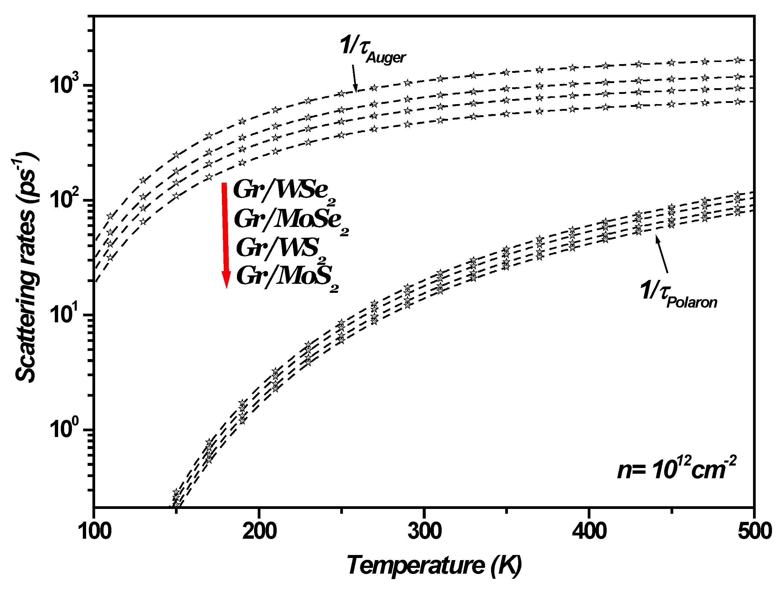
Figure 10 shows the Auger and SOP scattering rates as a function of temperature in 1LG/TMDCs interfaces, with a charge carrier density of . The results confirm that at room temperature and higher, the Auger and SOP scattering rates increase significantly, whereas at lower temperatures, the effect of both Auger and SOP scattering are minimal.
The calculated scattering rates approach constant values as temperature (Figure 10) increases. This behavior has been observed and discussed in Refs. [13,14,15,43] in which transport in graphene on polar substrates was investigated under both low and high bias conditions. Specifically, these studies highlighted that low-field mobility converges to a constant value as temperature rises. In the diffusive transport regime, this convergence is attributed to current saturation. While elastic scattering governs low-field mobility, current saturation is linked to inelastic scattering involving either surface polar phonons (SPPs) of the polar substrate or the intrinsic optical phonons of graphene. Furthermore, high-bias measurements in graphene, as noted in Ref. [43], revealed that the magnitude of the saturated current is determined by the energy of the optical phonons responsible for the saturation. Consequently, this saturation induces a convergence of scattering rates in graphene on polar substrates as temperature increases. In the present study, this behavior is demonstrated by the convergence of both Auger and SOP scattering rates at graphene/transition metal dichalcogenides (TMDCs) interfaces, as shown in Figure 10.
In graphene/transition metal dichalcogenide (TMDC) heterostructures, current saturation arises primarily due to inelastic scattering mechanisms. Key contributors include interactions with surface optical phonons at the TMDCs interfaces and intrinsic optical phonons in graphene. Additionally, electron overheating at elevated electronic temperatures contributes significantly to this saturation. In this state, the system stabilizes in a dynamic equilibrium where further increases in the electric field do not result in higher current.
Beyond transport phenomena, the optical properties of graphene/TMDC interfaces are also significantly influenced by two critical mechanisms: Auger recombination and interactions with surface optical phonons (SOPs). Auger processes, particularly at high carrier densities or in defect-rich materials, can reduce photoluminescence. While this behavior is a limitation for light-emitting devices, it can enhance carrier multiplication in applications such as photodetectors. In hybrid systems like graphene-TMDC heterostructures, interlayer coupling and external fields provide a unique platform to modulate Auger dynamics and phonon interactions, enabling innovative opportunities in quantum and optoelectronic devices.
5. Conclusion
In conclusion, firstly, we have investigated the impact of electron-surface optical phonon interactions in monolayer graphene-TMDCs heterostructures. For this, we utilized the eigenenergies derived from the tight-binding Hamiltonian. Our study explored the influence of various TMDCs on the SO phonon-limited mobility; conductivity, resistivity, and scattering rates in 1LG/TMDCs interfaces, considering the effects of SO phonon scattering. These transport properties are temperature-dependent, with the surface optical phonon scattering becoming more significant at higher temperatures. We have shown that at elevated temperatures, SO phonon scattering is the dominant scattering mechanism in graphene-TMDCs heterostructures. At room temperature and beyond, the SO phonon scattering rate is notably increased. The surface optical phonon in graphene-TMDC interface generates an electric field that couples with the electrons on the nearby graphene. This interaction results in a resonant coupling between the electronic sub-levels and the surface vibration modes, causing the Rabi splitting of electron levels. In summary, our findings indicate that the electron-surface optical phonon interaction is significantly influenced by the choice of TMDC.
Secondly, we have theoretically demonstrated that at room temperature and above, both Auger and SOP (surface optical phonon) scattering rates at the 1LG/TMDCs interfaces increase significantly, eventually converging to constant values as the temperature rises. In contrast, at lower temperatures, the impact of both Auger and SOP scattering is minimal. In conclusion, our findings emphasize that Auger recombination and SOP interactions are strongly influenced by the choice of specific TMDC material.
Finally, Van der Waals heterostructures (vdWHs) combining monolayer graphene (1LG) with transition metal dichalcogenides (TMDCs) exhibit outstanding electronic and optical properties, making them promising candidates for next generation nanoelectronic and optoelectronic devices. The performance of these heterostructures is significantly influenced by electron-surface optical phonon (SOP) interactions and Auger recombination processes, which govern charge carrier dynamics.
Author Contributions
Conceptualization, visualization M.M., R.B.., and S.G.; methodology, M.M; investigation, formal analysis, M.M..; writing—original draft preparation, M.M.; writing—review and editing, M.M.., R.B.., and S.G..; supervision, S.G. All authors have read and agreed to the published version of the manuscript.
Funding
This research received no funding.
Institutional Review Board Statement
Not applicable.
Informed Consent Statement
Not applicable.
Data Availability Statement
The data presented in this study are available on request from the corresponding author. The data are not publicly available due to privacy issues.
Conflicts of Interest
The authors declare no conflict of interest.
References
- Yang J.; Tang L.; Luo W.; Feng S.; Leng C.; Shi H.; Wei X. Interface engineering of a silicon/graphene heterojunction photodetector via a diamond-like carbon interlayer. ACS Appl. Mater. Interfaces 2021, 13, 4692–4702. [CrossRef]
- Xia F.;Wang H.; Jia Y. Rediscovering black phosphorus as an anisotropic layered material for optoelectronics and electronics. Nat. Commun. 2014, 5, 4458. [CrossRef]
- Geim A. K.; Grigorieva I. V. Van derWaals heterostructures. Nature 2013, 499, 419–425.
- Akinwande D.; Huyghebaert C.; Wang C. H.; Serna M. I.; Goossens S.; Li L. J.; Wong H. P.; Koppens F. H.L. Graphene and two-dimensional materials for silicon technology. Nature 2019, 573, 507−518. [CrossRef]
- Liu Y.; Duan X.; Shin H. J.; Park S.; Huang Y.; Duan X. Promises and prospects of two-dimensional transistors. Nature 2021; 591, 43−53. [CrossRef]
- M. Huang; S. Li; Z. Zhang; X. Xiong; X. Li and Y. Wu. Multifunctional high-performance van der Waals heterostructures. Nat. Nanotechnol. 2017, 12, 1148–1154. [CrossRef]
- L. Mao; C. C. Stoumpos and M. G. Kanatzidis. Two dimensional hybrid halide perovskites: principles and promises. J. Am. Chem. Soc. 2019, 141, 1171–1190. [CrossRef]
- K. Wei; Y. Sui and Z. Xu; et al. Acoustic phonon recycling for photocarrier generation in graphene–WS2 heterostructures. Nat. Commun. 2020, 11, 3876. [CrossRef]
- H. K. Ng; D. Xiang and A. Suwardi; et al. Improving carrier mobility in two-dimensional semiconductors with rippled materials. Nat. Electronics 2022, 5, 489–496. [CrossRef]
- S. Aeschlimann and A. Rossi; et al. Direct evidence for efficient ultrafast charge separation in epitaxial WS2/graphene heterostructures. Sci. Adv. 2020, 6,20. [CrossRef]
- T. Pandey; A. P. Nayak; J. Liu; S. T. Moran; J-S Kim; L-J Li; J-F Lin; D. Akinwande and A. K. Singh. Pressure-Induced Charge Transfer Doping of Monolayer Graphene/MoS2 Heterostructure. Small 2016, 12, 4063–4069. [CrossRef]
- Junnan Guo; Xinyue Dai; Lishu Zhang and Hui Li. Electron Transport Properties of Graphene/WS2 Van Der Waals Heterojunctions. Molecules 2023, 28, 6866. [CrossRef]
- M. Mahdouani. Investigation of the electron-surface phonon interaction effects in graphene on a substrate made of polar materials. PHYSE 2017, 87, 192-198. [CrossRef]
- M. Mahdouani ; S. Gardelis ; R. Bourguiga. The effect of Si impurities on the transport properties and the electron-surface phonon interaction in single layer graphene deposited on polar substrates. Physica B: Condensed Matter 2018, 550, 171–178. [CrossRef]
- M.Mahdouani; R.Bourguiga. Auger and carrier-surface phonon interaction processes in graphene on a substrate made of polar materials. Superlattices and Microstructures 2017, 102, 212-220. [CrossRef]
- Mounira Mahdouani; Ramzi Bourguiga and Spiros Gardelis. A Theoretical Study of the Electron–Surface Optical Phonon Interaction in Monolayer Transition Metal Dichalcogenides Deposited on SiC and hexagonal BN Dielectric Substrates in the Vicinity of the Points K+(K−) of the Brillouin Zone. Materials 2024,17, 5552. [CrossRef]
- M. Mahdouani; S. Gardelis; and A. G. Nassiopoulou. Role of surface vibration modes in Si nanocrystals within light emitting porous Si at the strong confinement regime. JOURNAL OF APPLIED PHYSICS 2011 , 110, 023527. [CrossRef]
- S. Gardelis ; A. G. Nassiopoulou ; M. Mahdouani ; R. Bourguiga; S. Jaziri. Enhancement and red shift of photoluminescence (PL) of fresh porous Si under prolonged laser irradiation or ageing: Role of surface vibration modes. Physica E 2009, 41, 986–989. [CrossRef]
- M. Mahdouani ; R. Bourguiga ; S. Jaziri. Polaronic states in Si nanocrystals embedded in SiO2 matrix. Physica E 2008, 41, 228–234. [CrossRef]
- Lee E. et al.. Direct CVD growth of a graphene/MoS2 heterostructure with interfacial bonding for two-dimensional electronics. Chem. Mater. 2020, 32, 4544–4552. [CrossRef]
- Tang Z. et al. A steep-slope MoS2/graphene dirac-source field-effect transistor with a large drive current. Nano Lett. 2021, 21, 1758–1764. [CrossRef]
- Li S. et al. Sandwich-like heterostructures of mos2/graphene with enlarged interlayer spacing and enhanced hydrophilicity as highperformance cathodes for aqueous zinc-ion batteries. Adv. Mater. 2021,33, 2007480. [CrossRef]
- Pomerantseva E. & Gogotsi Y. Two-dimensional heterostructures for energy storage. Nat. Energy 2017,2,17089. [CrossRef]
- Bag A. & Lee N-E. Gas sensing with heterostructures based on twodimensional nanostructured materials: a review. J. Mater. Chem.C 2019, 7, 13367–13383. [CrossRef]
- Choi H. K. et al. Gas molecule sensing of van der Waals tunnel field effect transistors Nanoscale 2017, 9, 18644–18650. [CrossRef]
- Swager T M & Mirica K. A. Introduction: Chemical sensors. Chem. Rev.2019, 119, 1–2. [CrossRef]
- Li Z. et al.. Recent advances of atomically thin 2D heterostructures in sensing applications. Nano Today 2021,40,101287. [CrossRef]
- Shin Y.; Kwon J.; Jeong Y.; Watanabe K., Taniguchi T.; Im S.; Lee G. H. Graphene Via Contact Architecture for Vertical Integration of vdW Heterostructure Devices. Small 2022, 18, 2200882. [CrossRef]
- Sun X.; Li X.; Zeng Y.; Meng L. Improving the stability of perovskite by covering graphene on FAPbI3 surface. Int. J. Energy Res. 2021, 45, 10808–10820. [CrossRef]
- Wang X.; Long R. Rapid charge separation boosts solar hydrogen generation at the graphene–MoS2 Junction: Time-domain Ab initio analysis. J. Phys. Chem. Lett.2021, 12, 2763–2769. [CrossRef]
- Wang H.; Gao S.; Zhang F.; Meng F.; Guo Z.; Cao R.; Zeng Y.; Zhao J.; Chen S.; Hu H. Repression of interlayer recombination by graphene generates a sensitive nanostructured 2D vdW heterostructure based photodetector. Adv. Sci. 2021, 8, 2100503. [CrossRef]
- Cong C.; Shang J.; Wang Y.; Yu T. Optical properties of 2D semiconductor WS2. Adv. Opt. Mater. 2018, 6, 1700767. [CrossRef]
- Zhen J.; Huang Q.; Liu Y.; Zhang S.; Dong H.; Lv K.; Qiu J. & Liu G. High carrier mobility and strong electron–phonon coupling in graphene–WS₂ heterobilayers under pressure. Journal of Materials Chemistry C 2023,11, 15555-15563. [CrossRef]
- Guillaume Froehlicher; Etienne Lorchat and Stéphane Berciaud. Charge Versus Energy Transfer in Atomically Thin Graphene-Transition Metal Dichalcogenide van der Waals Heterostructures. Phys. Rev. X 2018, 8, 011007. [CrossRef]
- Byung-Il Noh; Salvio Reza; Cassie Hardy; Cassie Hardy; Jiahan Li; Adib Taba; Masoud Mahjouri-Samani; James H. Edgar and Siyuan Dai. Low Dielectric Medium for Hyperbolic Phonon Polariton Waveguide in van der Waals Heterostructures. Nanomaterials 2024, 14, 1344. [CrossRef]
- Wugang Liao; Siwen Zhao; Feng Li; Cong Wang ; Yanqi Ge; Huide Wang; Shibo Wang and Han Zhang. Interface engineering of two-dimensional transition metal dichalcogenides towards next-generation electronic devices: recent advances and challenges. Nanoscale Horiz. 2020, 5, 787-807. [CrossRef]
- Leonardo Martini;Vaidotas Mišeikis;David Esteban;Jon Azpeitia;Sergio Pezzini; Paolo Paletti; Michał W. Ochapski;Domenica Convertino; Mar Garcia Hernandez; Ignacio Jimenez and Camilla Coletti. Scalable High-Mobility Graphene/hBN Heterostructures. ACS Applied Materials & Interfaces 2023,15, 37794-37801. [CrossRef]
- Novoselov K. S.; Geim A. K.; Morozov S. V.; Jiang D.; Katsnelson M. I.; Grigorieva I. V.; Dubonos S. V. ; Firsov A. A. Two-dimensional gas of massless Dirac fermions in graphene. Nature 2005, 438, 197. [CrossRef]
- Zhang Y.; Tan Y. W.; Stormer H. L.; Kim P. Experimental observation of the quantum hall effect and Berry’s phase in graphene. Nature 2005, 438, 201. [CrossRef]
- Yuanzheng Li; Jia Shi; Heyu Chen; Rui Wang; Yang Mi; Cen Zhang; Wenna Du; Shuai Zhang; Zheng Liu; Qing Zhang; Xiaohui Qiu; Haiyang Xu; Weizhen Liu; Yichun Liu and Xinfeng Liu. The Auger process in multilayer WSe2 crystals. Nanoscale 2018, 10, 17585-17592. [CrossRef]
- Yingqi Tang; Hao Li; Xiaotong Mao; Ju Xie; Jin Yong Lee and Aiping Fu. Bidirectional heterostructures consisting of graphene and lateral MoS2/WS2 composites: a firstprinciples study. RSC Adv.2019 ,9, 34986-34994. [CrossRef]
- Huijuan Geng; Di Yuan; Zhi Yang; Zhenjie Tang; Xiwei Zhang; Kui Yang and Yanjie Su. Graphene van der Waals heterostructures for high-performance photodetectors. J. Mater. Chem. C 2019, 7, 11056-11067. [CrossRef]
- Vasili Perebeinos; Phaedon Avouris. Inelastic scattering and current saturation in graphene PHYSICAL REVIEW B 2010, 81, 195442. [CrossRef]
- M. V. Fischetti; D. A. Neumayer and E A Cartier. Effective electron mobility in Si inversion layers in metal–oxide–semiconductor systems with a high-κ insulator: The role of remote phonon scattering. J. Appl.Phys. 2001, 90, 4587. [CrossRef]
- V. Rozhkov ; Franco Nori. Exact wave functions for an electron on a graphene triangular quantum dot. PHYSICAL REVIEW B 2010, 81, 155401. [CrossRef]
- Gabriel Antonius and Steven G Louie. Theory of exciton-phonon coupling. Phys. Review B 2022, 105, 085111. [CrossRef]
- Thibault Sohier; Matteo Calandra; and Francesco Mauri. Two-dimensional Fröhlich interaction in transition-metal dichalcogenide monolayers: Theoretical modeling and first-principles calculations. Phys. Rev. B 2016,94,085415. [CrossRef]
- Yixiong Wang ; Chenglin He ; Qin Tan ; Zilan Tang ; Lanyu Huang ; Liang Liu ; Jiaocheng Yin; Ying Jiang ; Xiaoxia Wang and Anlian Pan. Exciton–phonon coupling in two-dimensional layered(BA)2PbI4perovskite microplates. RSC Adv. 2023, 13, 5893–5899. [CrossRef]
- Jinlong Ma; Dongwei Xu; Run Hu ; Xiaobing Luo. Examining two-dimensional Fröhlich model and enhancing the electron mobility of monolayer InSe by dielectric engineering. Journal of Applied Physics 2020, 128, 035107. [CrossRef]
- Nicki Frank Hinsche and Kristian Sommer Thygesen. Electron–phonon interaction and transport properties of metallic bulk and monolayer transition metal dichalcogenide TaS2. 2D Materials 2017, 5, 015009. [CrossRef]
- Xiao Y ; Li ZQ ; Wang Z W. Polaron effect on the bandgap modulation in monolayer transition metal dichalcogenides. J. Phys.Cond. Matter 2017, 29, 485001. [CrossRef]
- J. V. Nguepnang ; C. Kenfack Sadem ; A. Kenfack Jiotsa ; M. F. C. Fobasso ; Y. Sun. Optical signature of bipolaron in monolayer transition metal dichalcogenides: all coupling approach. Optical and Quantum Electronics 2021, 53, 728. [CrossRef]
- Devreese J. T.; Huybrechts W.; Lemmeks L. On the optical absorption of free polarons at weak coupling. Physica Status Solidi (b) 1971, 48,77–86. [CrossRef]
- Daniela L. Mafra and Paulo T. Araujo. Intra- and Interlayer Electron-Phonon Interactions in 12/12C and 12/13C BiLayer Graphene. Appl. Sci.2014, 4, 207-239. [CrossRef]
- S. Q. Wang and G. D. Mahan. Electron Scattering from Surface Excitations. Phys. Rev. B 1972, 6, 4517. [CrossRef]
- D. Van Tuan; A. M. Jones; M. Yang; X. Xu and H. Dery. Virtual Trions in the Photoluminescence of Monolayer Transition-Metal Dichalcogenides. Phys.Rev.lett. 2019, 122, 217401. [CrossRef]
- Z. Jin; X. Li; J. T. Mullen and K. W. Kim. Intrinsic Transport Properties of Electrons and Holes in Monolayer Transition Metal Dichalcogenides. Phys. Rev. B 2014, 90, 045422. [CrossRef]
- H. Dery and Y. Song. Polarization analysis of excitons in monolayer and bilayer transition-metal dichalcogenides. Phys. Rev. B 2015, 92, 125431. [CrossRef]
- M. Danovich; I. L. Aleiner; N. D. Drummond; V. I. Falko. Fast relaxation of photo-excited carriers in 2-D transition metal dichalcogenides. IEEE Journal of Selected Topics in Quantum Electronics 2017, 23, 6000105. [CrossRef]
- Sanjay Gopalan; Maarten L. Van de Put; Gautam Gaddemane; and Massimo V. Fischetti. Theoretical Study of Electronic Transport in Two-Dimensional Transition Metal Dichalcogenides: Effects of the Dielectric Environment. Phys. Rev. Applied 2022,18, 054062. [CrossRef]
- Julian F. R. V. Silveira; Rafael Besse; and Juarez L. F. Da Silva. Stacking Order Effects on the Electronic and Optical Properties of Graphene/Transition Metal Dichalcogenide Van der Waals Heterostructures. ACS Applied Electronic Materials 2021,3, 1671–1680. [CrossRef]
- Rui Zhang; Guoqiang Hao; Xiaojun Ye; Shangpeng Gao and Hongbo L. Tunable electronic properties and Schottky barrier in a graphene/WSe2 heterostructure under out-of-plane strain and an electric field. Phys. Chem. Chem. Phys. 2020, 22, 23699-23706. [CrossRef]
- V. Rozhkov; Franco Nori. Exact wave functions for an electron on a graphene triangular quantumdot. PHYSICAL REVIEW B 2010, 81,155401. [CrossRef]
- L. X. Benedict; S. G. Louie; and M. L. Cohen. Static polarizabilities of single-wall carbon nanotube. Phys. Rev. B 1995, 52, 8541. [CrossRef]
- M. Mahdouani; R. Bourguiga; S. Jaziri ; S. Gardelis ; A. G. Nassiopoulou. Investigation of Auger recombination in Ge and Si nanocrystals embedded in SiO2 matrix. Physica E 2009, 42, 57–62. [CrossRef]
- M.Mahdouani; R. Bourguiga; S. Jaziri; S. Gardelis; and A. G. Nassiopoulou. Auger recombination in silicon nanocrystals embedded in SiO2 wide band-gap lattice. phys. stat. sol. (a) 2008, 205, 2630. [CrossRef]
- H. Castro Neto; F. Guinea; N. M. R. Peres; K. S. Novoselov; and A. K. Geim. The electronic properties of graphene. Rev. Mod. Phys. 2009, 81, 109. [CrossRef]
- N. M. R. Peres. Colloquim:The transport properties of graphene: An introduction. Rev. Mod. Phys. 2010, 82, 2673. [CrossRef]
- S. Das Sarma; S. Adam; E. H. Hwang; and E. Rossi. Electronic transport in two-dimensional graphene. Rev. Mod.Phys.2011, 83,407. [CrossRef]
- V. N. Kotov; B. Uchoa; V. M. Pereira; F. Guinea; and A. H. Castro. Electron- Electron Interactions in Graphene: Current Status and Perspectives. Neto Rev. Mod. Phys. 2012, 84, 1067. [CrossRef]
- Andrea Tomadin; Daniele Brida; Giulio Cerullo; Andrea C. Ferrari; and Marco Polini. Nonequilibrium dynamics of photoexcited electrons in graphene. PHYSICAL REVIEW B 2013, 88, 035430. [CrossRef]
Figure 1.
Side view of 1LG/MoSe2 heterostructure. The gray, orange, cyan full circles represent the C, Se, and Mo atoms, respectively and d is the vdWHs distance.
Figure 1.
Side view of 1LG/MoSe2 heterostructure. The gray, orange, cyan full circles represent the C, Se, and Mo atoms, respectively and d is the vdWHs distance.
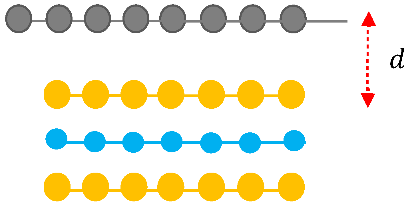
Figure 2.
SO phonon-limited mobility, , versus the temperature in 1LG/TMDCs (Gr/TMDCs) interfaces. The charge carrier density .
Figure 2.
SO phonon-limited mobility, , versus the temperature in 1LG/TMDCs (Gr/TMDCs) interfaces. The charge carrier density .
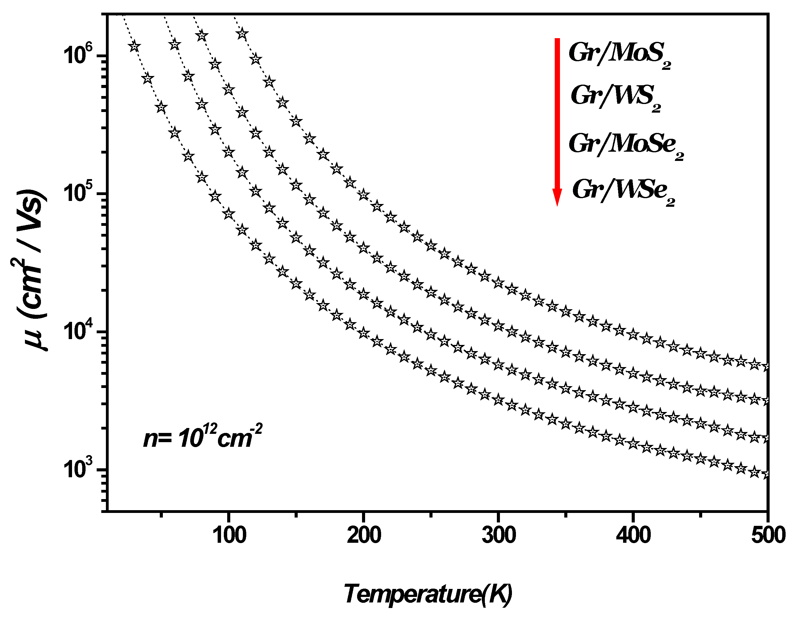
Figure 3.
SO phonon-limited resistivity, , versus the temperature in 1LG/TMDCs (Gr/TMDCs) interfaces. The charge carrier density .
Figure 3.
SO phonon-limited resistivity, , versus the temperature in 1LG/TMDCs (Gr/TMDCs) interfaces. The charge carrier density .
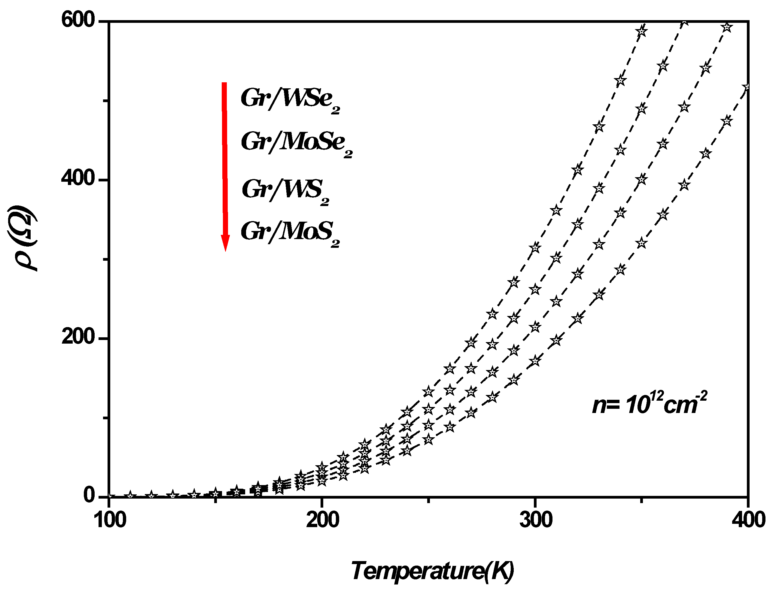
Figure 4.
SO phonon-limited conductivity, , versus the charge carrier density in 1LG/TMDCs (Gr/TMDCs) interfaces at T=300 K.
Figure 4.
SO phonon-limited conductivity, , versus the charge carrier density in 1LG/TMDCs (Gr/TMDCs) interfaces at T=300 K.
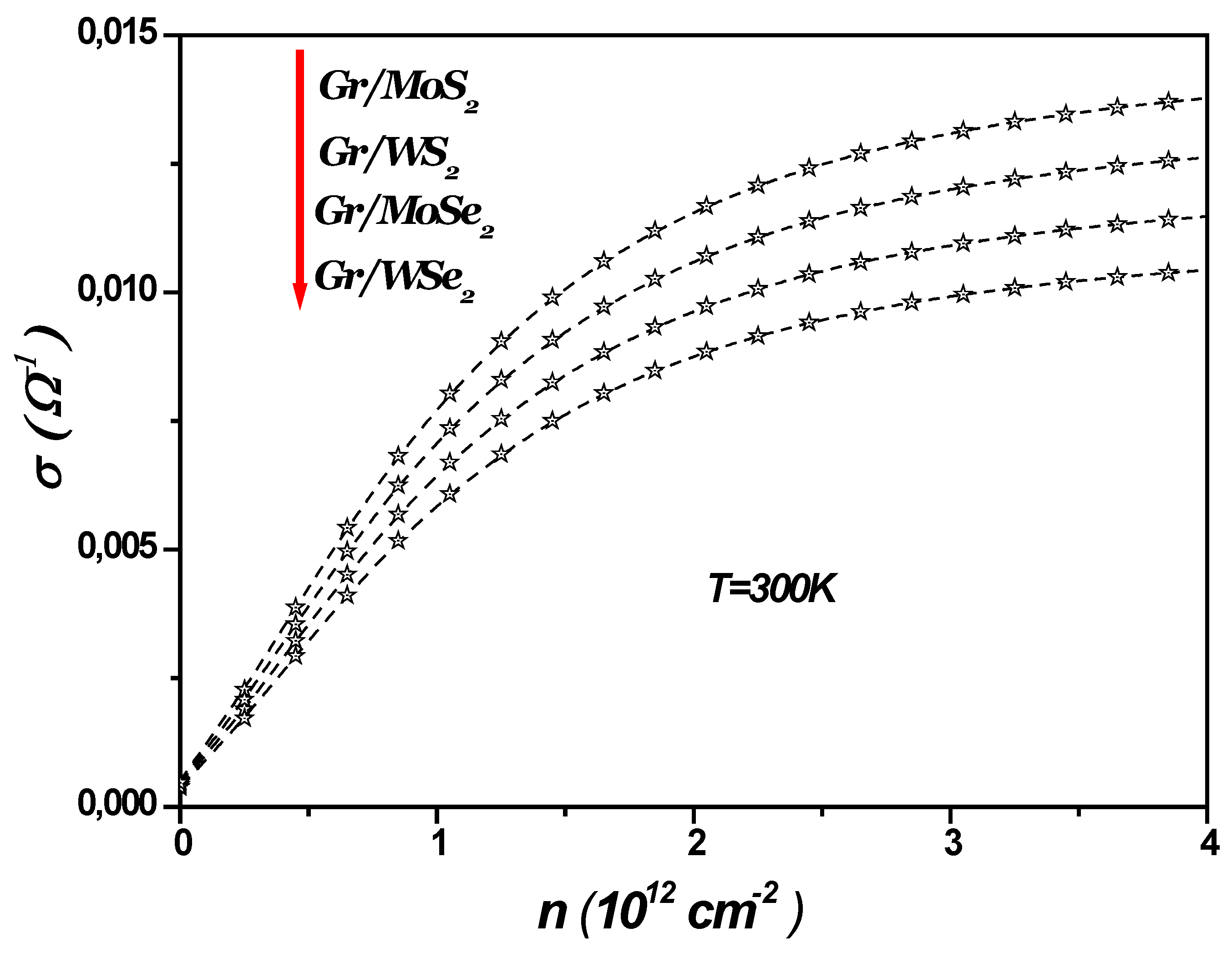
Figure 5.
The scattering rate versus the temperature in 1LG/TMDCs (Gr/TMDCs) interfaces. The charge carrier density .
Figure 5.
The scattering rate versus the temperature in 1LG/TMDCs (Gr/TMDCs) interfaces. The charge carrier density .
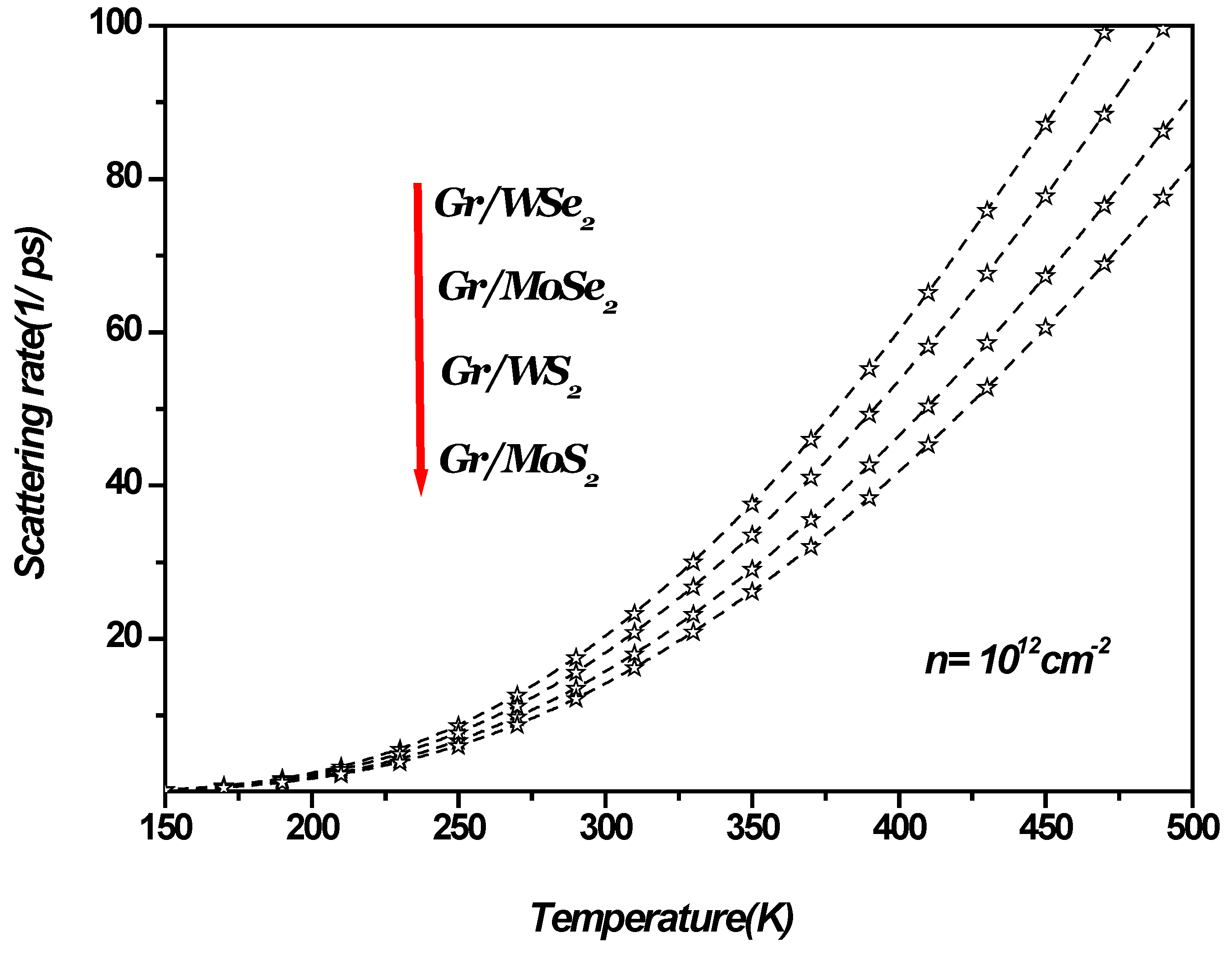
Figure 6.
Left: Lattice structure of graphene, made out of two interpenetrating triangular lattices a1 and a2 are the lattice unit vectors; Right: corresponding Brillouin zone. The Dirac cones are located at the K and K’ points.
Figure 6.
Left: Lattice structure of graphene, made out of two interpenetrating triangular lattices a1 and a2 are the lattice unit vectors; Right: corresponding Brillouin zone. The Dirac cones are located at the K and K’ points.
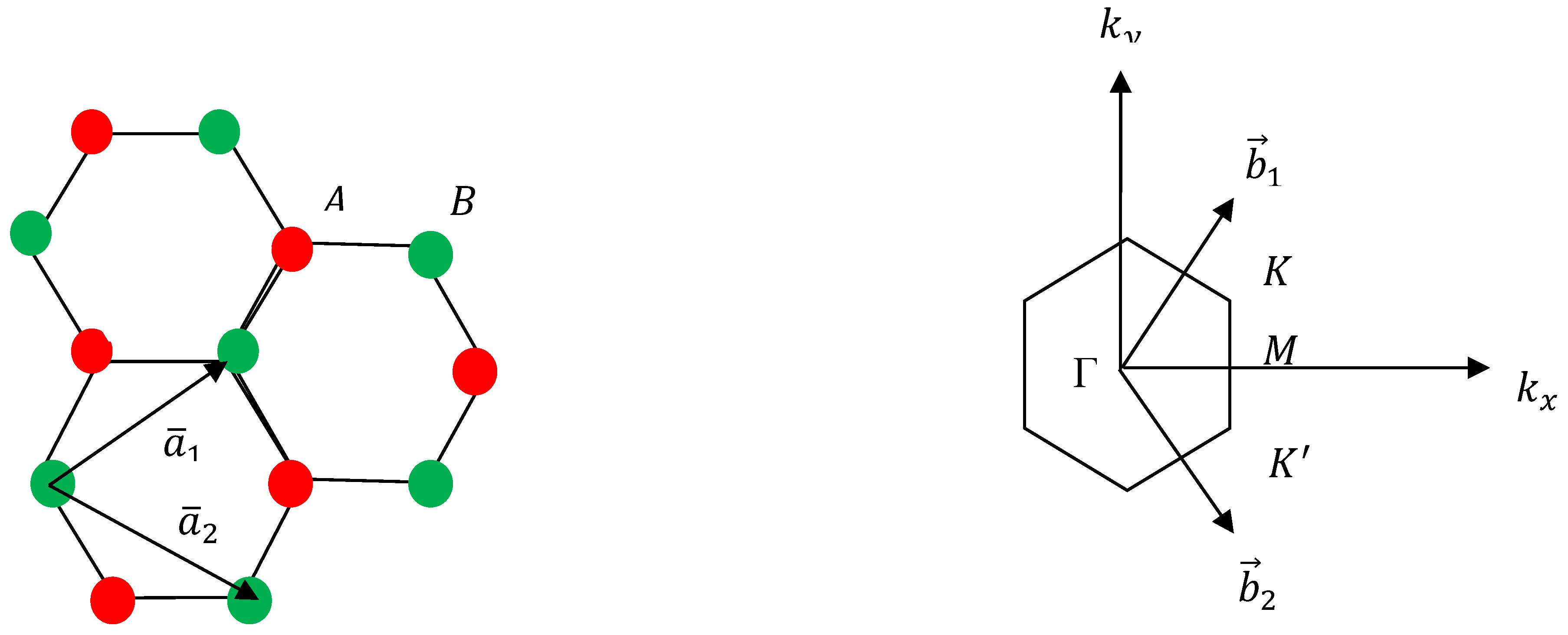
Figure 7.
The variation of the SOP coupling versus in 1LG/TMDCs interfaces. The wave vector changes along the Γ-K direction. K is the Dirac point and.
Figure 7.
The variation of the SOP coupling versus in 1LG/TMDCs interfaces. The wave vector changes along the Γ-K direction. K is the Dirac point and.
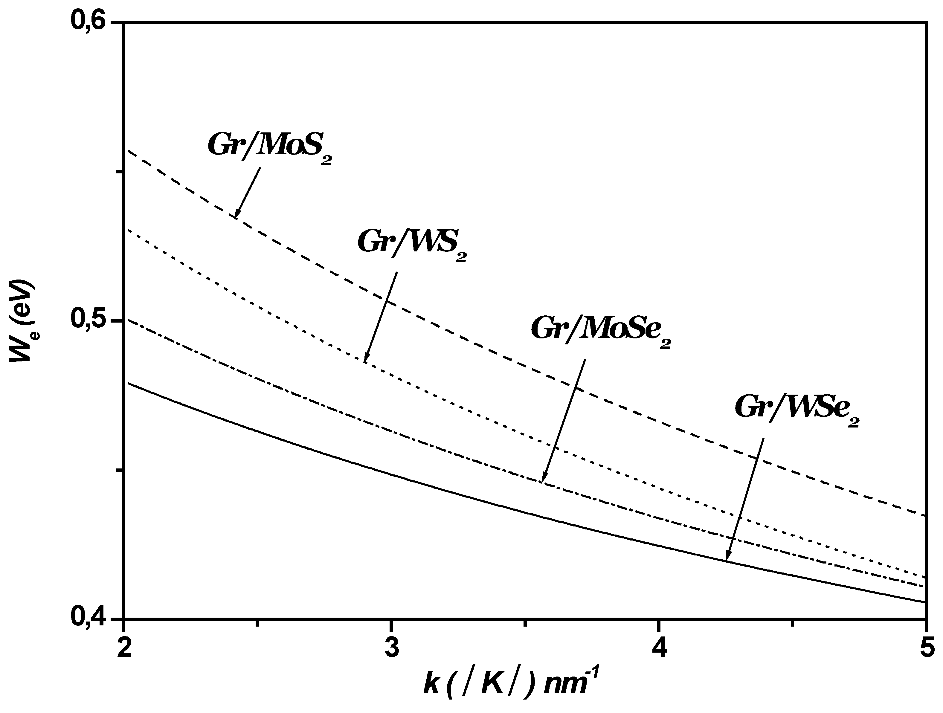
Figure 8.
a, b, c, d). Polaron electron energies vs in 1LG/TMDCs (Gr/TMDCs) interfaces. The wave vector changes along the Γ-K direction. K is the Dirac point and.
Figure 8.
a, b, c, d). Polaron electron energies vs in 1LG/TMDCs (Gr/TMDCs) interfaces. The wave vector changes along the Γ-K direction. K is the Dirac point and.
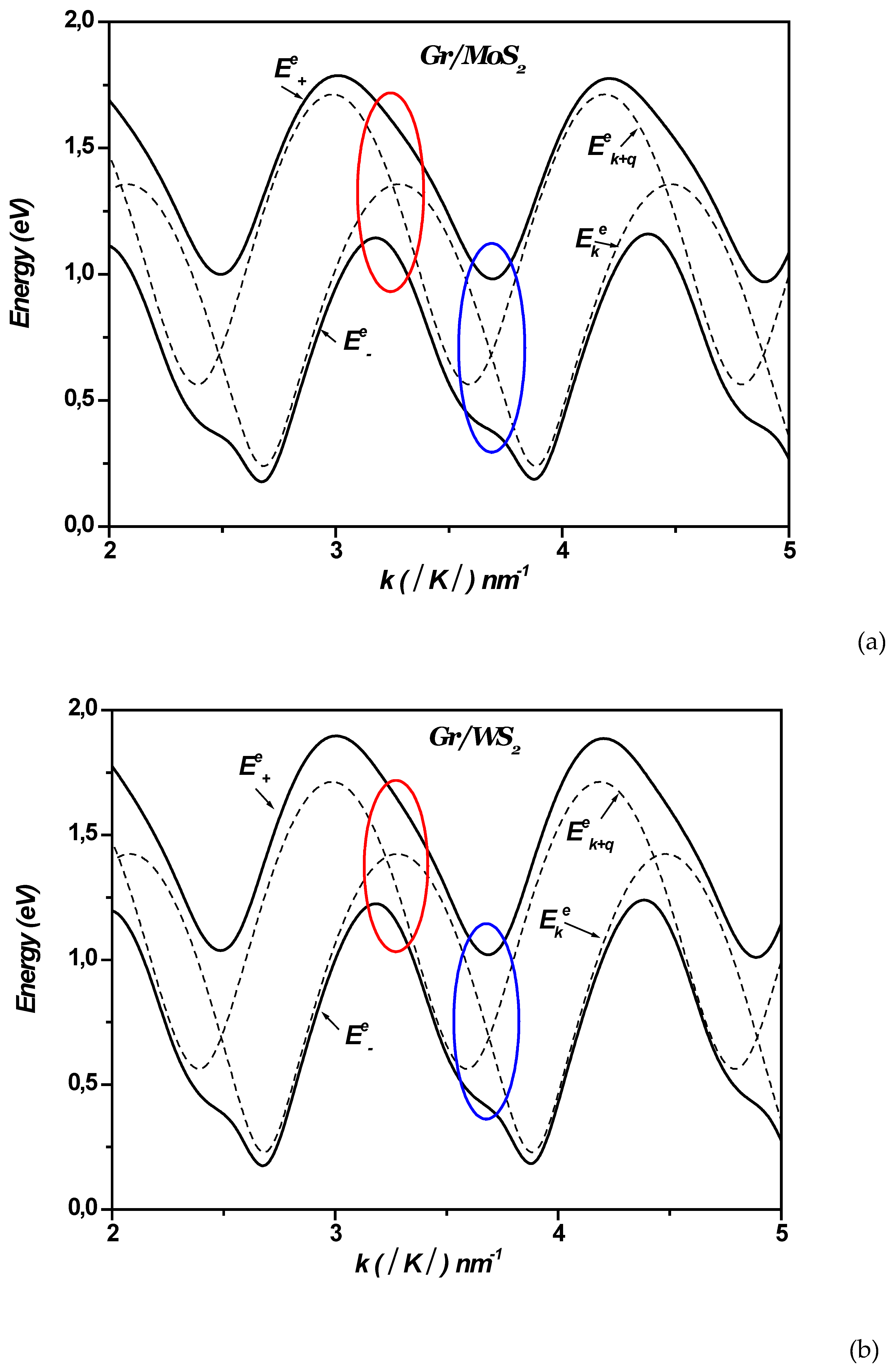
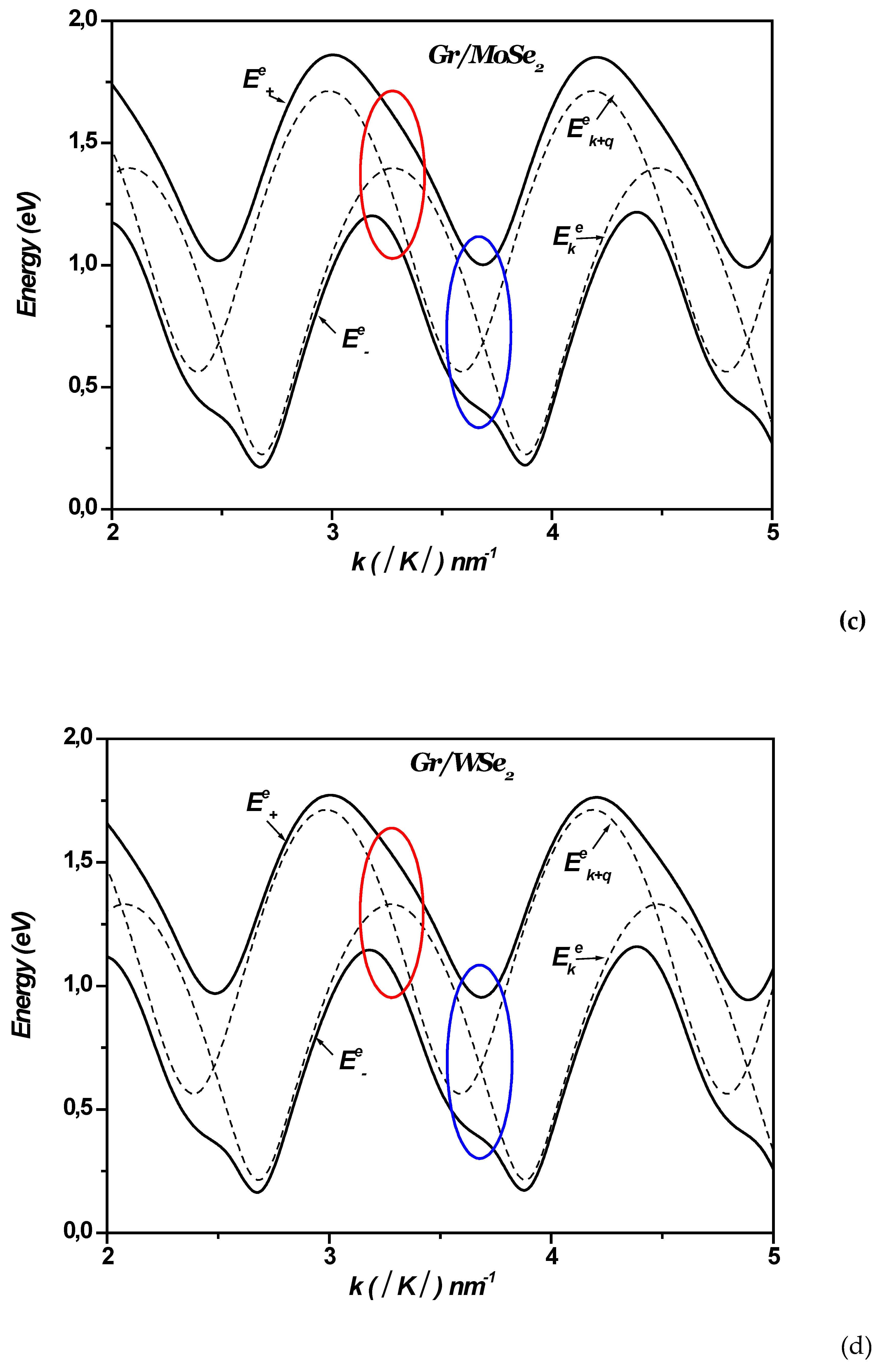
Figure 9.
The noninteracting states and cross periodically near and ( is an integer) in 1LG/TMDC (Gr/TMDC) interface. The wave vector changes along the Γ-K direction. K is the Dirac point and. Right: zoom-in of the regions (a) and (b).
Figure 9.
The noninteracting states and cross periodically near and ( is an integer) in 1LG/TMDC (Gr/TMDC) interface. The wave vector changes along the Γ-K direction. K is the Dirac point and. Right: zoom-in of the regions (a) and (b).
Figure 10.
Auger and SOP scattering rates as a function of temperature in 1LGr/TMDCs interfaces, with a charge carrier density of .
Figure 10.
Auger and SOP scattering rates as a function of temperature in 1LGr/TMDCs interfaces, with a charge carrier density of .

Disclaimer/Publisher’s Note: The statements, opinions and data contained in all publications are solely those of the individual author(s) and contributor(s) and not of MDPI and/or the editor(s). MDPI and/or the editor(s) disclaim responsibility for any injury to people or property resulting from any ideas, methods, instructions or products referred to in the content. |
© 2025 by the authors. Licensee MDPI, Basel, Switzerland. This article is an open access article distributed under the terms and conditions of the Creative Commons Attribution (CC BY) license (http://creativecommons.org/licenses/by/4.0/).
Copyright: This open access article is published under a Creative Commons CC BY 4.0 license, which permit the free download, distribution, and reuse, provided that the author and preprint are cited in any reuse.


