

Submitted:
09 August 2024
Posted:
10 August 2024
You are already at the latest version
Abstract
For semiconducting two-dimensional transition metal dichalcogenides, carrier transport proper-ties of the material are affected by strain engineering. In this work, we investigate the carrier mo-bility of monolayer hafnium disulphide (HfS2) under different biaxial strains by first-principles calculations combined with Kubo-Greenwood mobility approach and compact band model. The decrease/increase in effective mass of conduction band of monolayer HfS2 caused by biaxial ten-sile/compressive strain is the major reason for the enhancement/degradation of its electron mobil-ity. Lower hole effective mass of valence bands in the monolayer HfS2 under biaxial compressive strain results in the better hole transport performance of monolayer HfS2 than the one with biaxial tensile strain. In summary, biaxial compressive strain decreases both effective mass and phonon scattering rate of monolayer HfS2, resulting in an increase in carrier mobility. When the biaxial compressive strain reaches 4%, for the conduction band of monolayer HfS2, electron mobility en-hancement ratio is ~90%. For the valence band of monolayer HfS2, the maximum hole mobility enhancement ratio appears ~13% at biaxial compressive strain of 4%. Our results indicate that the carrier transport performance of monolayer HfS2 can be greatly improved by the strain engineer-ing.
Keywords:
mobility
; strain
; Kubo-Greenwood mobility approach
; hafnium disulphide (HfS2)
1. Introduction
Since the thickness of TMD can be pushed down to less than a few nanometers, TMD is promising alternative channel materials for realizing ultra-thin body field effect transistors (FET) which are robust to short channel effects. TMD is divided into two kinds of crystal structures of trigonal prismatic (2H-TMD type) and octahedral (1T-TMD type). MoS2 is typical TMD with a 2H-TMD type structure. TMD with the 1T-TMD type (group space P3m1) structure has a much lower lattice thermal conductivity and a better thermoelectric performance at room temperature. This implies that HfS2 is a good 2D thermoelectric material. Hao Wang et al. predicted that the lattice thermal conductivity of bulk HfS2 is much smaller than it of MoS2, making the HfS2 system a promising thermoelectric material [1]. They also investigated the thermoelectric properties of monolayer HfS2 and demonstrated that monolayer HfS2 is an excellent n-type thermoelectric material, with much improved thermoelectric performance compared with the bulk. Furthermore, the valence band valleys in monolayer HfS2 can be tuned by the external biaxial tensile strain owing to the degeneracy of the valence band valleys reaching the maximum at strain value of 6%. Monolayer HfS2 like CdI2-type structure has become well-known due to its low lattice thermal conductivity resulting in promising applications in thermoelectric [2]. Hongyan Guo et al. performed a systematic first-principles study of the effect of tensile strains on the electronic properties of early monolayer TMD and suggested that the tensile strain could significantly affect the electronic properties of many early TMDs in general and the electronic bandgap in particular [3]. For group IVB TMD such as HfS2, the bandgap increased with the biaxial tensile strain while starting to decrease at strain 6~8%. Their investigation suggested that strain engineering was an effective approach to modify electronic properties of TMD such as monolayer HfS2, thereby opening an alternative way for future electronic applications. Recently, Mayuri Sritharan et al. pointed out that transition metal dichalcogenides (TMD) monolayers with native high-κ oxides presented a new avenue towards the development of new generation field-effect transistor (FET) devices [4]. These TMD materials experimentally showed to form a natively compatible high dielectric oxide layer, which could enhance both transistor device scaling and the supply voltage shrinking. They found that monolayer hafnium disulphide (HfS2) exhibited isotropic transport at channel length of 10 nm with ON currents over 1000 μA/μm and good subthreshold swing and identified monolayer HfS2 as a superior material within this TMD family for ultra-scaled FET.
Dr. A. Afzalian’s research team from imec developed an atomistic-modelling solver (ATOMOS) to assess the physics and fundamental-performance potential of monolayer HfS2 FET down to a gate length of 5 nm, including the effect of carrier phonon scattering [5,6]. They predicted that the monolayer HfS2 FET had good scalability down to gate length of 5 nm with a promising high on current level. They also proposed a concept of dynamically doped 2D FET, that scaled better than other 2D FET counterpart. Used in the combination with a best mobility material such as monolayer HfS2, it allowed for keeping the excellent performance on drive current and competitive energy-delay. In Ref. [7], Dr. Jiwon Chang investigated ballistic transport characteristics of monolayer HfS2 FET via quantum transport simulation. He focused on the role of degenerate conduction band (CB) valleys in monolayer HfS2 and predicted that the effect of channel orientation on device performances was much weaker in monolayer HfS2 FET owing to the degenerate CB valleys of monolayer HfS2.
Toru Kanazawa et al. first experimentally evaluated the FET performance of HfS2 and revealed its potential for transistor channel [8]. In addition, the other properties of HfS2 were not thoroughly investigated and they also reported some basic characteristics of HfS2 essential for FET device fabrication. Continuous efforts to seek for other 2-D materials lead to the discovery of anisotropic 2-D material. Unlike Mo-based TMD, HfS2 is characterized with its highly anisotropic conduction band. Theoretical investigations of HfS2 FETs have been performed [5,6,7]. Anisotropic 2-D materials other than phosphorene, Hf-based TMDs, have been explored by density functional theory (DFT) calculations [9,10]. Monolayers of Hf-based TMD such as HfS2, are quite different from those of Mo-based TMD because of different crystal symmetry and atomic bonding. They have indirect band gaps with three-fold degenerate conduction band (CB) valleys whose dispersions around the minimum of CB are highly anisotropic. Among Hf-based TMDs, monolayer HfS2 exhibits sizable band gaps, larger than 1 eV, suitable for nanoscale FET applications. In this work, we present a comprehensive computational study of carrier mobility of monolayer HfS2 through the first principle method, compact band model and Kubo-Greenwood mobility approach. We discuss the influence of band structure anisotropy of monolayer HfS2 on carrier transport performances as well as the strain engineering of monolayer HfS2.
As a member of 1T-MX2, the carrier transport performance of monolayer HfS2 deserves to be further explored and improved. Although its carrier transport performance has been reported, there is few studies about the effects of the strain on this topic. Strain effects on materials can tune their electronic band degeneracy and thus broaden carrier transport properties. In the present work, we use DFT accompanied by Boltzmann transport theory and deformation potential theory to study the strain effect on the carrier transport properties of monolayer HfS2. The results indicate that the carrier effective mass is highly shrinking when the biaxial compressive strain gets 4%. As a consequence, the carrier mobility reaches the highest value for both electron and hole. In this case, we surprisingly discovery that the highest mobility value is owing to carrier effective mass shrinking.
The effect of strain on the band structure and bandgap of monolayer HfS2 has been investigated in previous studies [11,12], showing that the application of tensile and compressive biaxial strain results in bandgap increasing and decreasing, respectively. Manouchehr Hosseini et al. studied the effect of strain on the mobility of monolayer MoS2 and found that the tensile biaxial strain could significantly enhance the mobility [13]; however, the investigation of a strain effect on the mobility of other 1T-TMD such as HfS2 was still missing. The conduction and valence band structures of HfS2 are different owing to indirect bandgap and the conduction band and valence band having different effective masses. In this work, we present a comprehensive analysis on the effect of biaxial strain on the mobility of monolayer HfS2, employing the first principle method for band structure calculations and then the Kobo-Greenwood mobility approach for evaluating carrier mobility [14,15]. The methodology for first principle method, compact band model, and Kobo-Greenwood mobility approach is briefly presented in Section 2. The effects of biaxial strain on the band structure and mobility of monolayer HfS2 are discussed in Section 3, and the concluding works are presented in Section 4.
2. Computational Methodology
This section explains the computational methodology for the evaluation of band structure, compact band model and carrier mobility.
2.1. Band Structure of Monolayer HfS2
Electronic structure calculations and structure optimization of monolayer HfS2 are performed through DFT calculations by QuantumATK [16] using the linear combination of pseudoatomic orbital method with the generalized gradient approximation (GGA) to describe the exchange-correlation functional. The plane wave energy cutoff is set 500 eV and the Brillouin zone is sampled by a 8× 8 × 1 mesh of the Monkhorst-Pack k points. All the atomic positions are completely relaxed until the Hellmann-Feynman forces converge to 0.005 eV/Å and energy to 1meV. We adopt a 13 Å vacuum layer along the z-axis to avoid the interaction between periodic images. Besides, we also take into account the Heyd-Scuseria-Ernzerhof (HSE06) functional for the band structure calculation. The phonon spectrum is also obtained by QuantumATK. Figure 1a shows the top and side views of monolayer HfS2 atomic structure. The band structure of monolayer HfS2 and the corresponding first Brillouin Zone (1st BZ) are shown in Figure 1b. Monolayer HfS2 is a layered material composed of vertically stacked S-Hf-S layers through van der Waals forces. Each single S-Hf-S layer consists of two hexagonal planes of S atoms and an intermediated hexagonal plane of Hf atoms. Note that HfS2 is A-B stacked in HfS2. We construct monolayer HfS2 structure by using the lattice parameter (a = 3.64 Å) which is close to the data from Ref. [12]. Highly anisotropic CB with its minimum located at the M-point is found as in Figure 1b. The calculated indirect band gap is 1.29 eV in close agreement with the previous theoretical prediction [11]. There are three conduction band (CB) valleys in the 1st BZ of monolayer HfS2 as seen in Figure 1(b). We extract electron effective masses of three M valleys in two directions of armchair (AR) and zigzag (ZA) by parabolic fitting of the band structure and list them in Table 1. In the direction AR (i.e. M’-Г), valley M’ has a very heavy effective mass mc = 2.45m0 with a light transverse effective mass, while the other two M valleys have light ones mc = 0.31m0. In the other direction ZA (i.e. M’-K), valley M’ exhibits a light effective mass mc = 0.24m0 with a heavy transverse effective mass and the other two M valleys show heavier effective masses mc = 0.74m0. The valence band structure of monolayer 1T-HfS2 along the Г-M and Г-K directions is also shown in Figure 1b, and corresponding contour plots near the conduction band (CB) minima and valence band (VB) maximum are shown schematically in Figure 2. The CB minima at each M-point are highly anisotropic, but the existence of three such valleys within the 1st BZ with rotational symmetry relaxes the overall direction-dependence of transport, leading to similar monolayer HfS2 n-type FET performance in the AR and ZA directions [7]. Conversely, the degenerate and nearly-isotropic heavy hole (HH) and light hole (LH) VB peaks are located at the Г point (Figure 1b) according to ab-initio calculation with GGA only, and spin-orbit coupling (SOC) breaks the degenerate at Г point and induced valence band HH and LH splitting via ab-initio calculation with GGA+SOC. Figure 2 shows CB contour plots for unstrained HfS2 with the corresponding band structures around the M point as shown in Figure 1b. We can characterize two types of effective mass, namely the effective mass mc in the transport direction and the density of states (DOS) effective mass mDOS. mc is calculated by fitting the curvature of the CB minimum/VB maxima in the transport direction. For example, mc of M’ valley along M-K direction (AR direction) equals mMK and mAR. Details about mc and mDOS are shown in Table 1. Formula of mDOS is followed by the definition from Ref. [17]. In unstrained HfS2, the mDOS of the valence band HH and LH are 0.47 m0 and 0.18 m0 as listed in Table 1, respectively. These values of effective mass for CB and VB of monolayer are in agreement with the results of Refs. [17,18]. The biaxial strain in this paper is defined as ε=(a−a0)/a0, where a0 and a are the equilibrium and deformed lattice constants, respectively. The effective mass of the carriers is calculated using the definition of Ref. [19].
2.2. Compact band Model
Band structure of both conduction and valence bands in monolayer HfS2 cannot be accurately described within simple effective mass approximation (EMA) model. First principle band structure calculated using GGA exhibits deviations from the parabolic dispersion at low energies, which yields energy-dependent DOS. Here, to describe the E-K dispersion of conduction band, we use the following implicit expression with energy-dependent effective mass (i.e. Rudenko model [20]).
where mx(E) and my(E) are energy dependent functions. After converting the coordinate into polar coordinate, Equation (1) becomes Equation (2).
when , we use to fit E-K relation along x direction and get the energy dependent effective mass, mx(E)
For ,we define the energy dependent effective mass, my(E) as below.
Finally, transfer Equation (2) to analytical form as Equation (5)
Arrange Equation (5) into the K(E,θ) form as Equation (6).
We summarize parameters used in the Rudenko model for the conduction band of monolayer HfS2 in Table 2.
For valence band, we adopt new compact model to fit first principle valence band structure of monolayer HfS2. Being opposite to common E-K relation, the form of K(E) is used, which could help the successive calculation of other key physical quantity such as density of states and energy contours for valence band. The form of new compact model for HfS2 shows
Two major parameters appear in the new compact model. Directionality (θ): for determining the direction of k moving towards various symmetry points. Energy effect: determined by A(E), C(E) functions. The form of functions A(E), C(E) is the combination of k in different directions. Monolayer HfS2 presents the sixth fold symmetry and boundary condition is EMA model with non-parabolic correction, so that
The form of k1, k2 could be acquired through boundary condition. In the equation, the coefficients of α, β, mi (i=1, 2) could be acquired by the fitting with first principle band structure. On the other hand, when θ is 0 and π/6, other relations could be acquired as shown in Equation (10-11), respectively.
It further solves and gives relationship between key energy-dependent parameters such as A(E), C(E) and k1, k2.
We summarize parameters used in the new compact model for the valence band of monolayer HfS2 in Table 3.
Finally, both Rudenko model and new compact model are the form of K(E,θ) and can be applied for calculating density of states per spin as shown in the Equation (14).
Reference [11] is followed to define the x component of group velocity square Vx2 (E) as shown in Equation (15).
2.3. Kubo-Greenwood Formula for Carrier Mobility
According to compact band structure as introduced in previous subsection, we calculate the carrier transport with the Kubo-Greenwood mobility formula [14,15]. Parameters used for carrier mobility calculation of monolayer HfS2 are presented in Table 4. Carrier mobility for monolayer HfS2 has been calculated using the momentum relaxation time approximation according to the Kubo–Greenwood formula [14,15]. The scattering mechanisms included in the calculation contain the phonon scatterings such as acoustic phonon and optical phonon. Once the relaxation times for the phonon-limited scattering mechanisms have been determined, the carrier mobility formula for each band, shown as follows, is calculated according to the Kubo–Greenwood formula
In Equation (16), f(E) denotes the Fermi–Dirac function, E is the total energy, Vx2(E) is the energy-dependent group velocity square along x direction, τ(E) is the scattering time, and D(E) is the density of states. E0 is band edge energy. The scattering time,, is found by summing all scattering rates considered as Equation (17-19).
where τADP(E) and τODP(E) are acoustic phonon and optical phonon scattering times, respectively. Nq is the Bose occupation of phonon ωop. Dac and Dop are deformation potential for acoustic and optical phonon, respectively. In monolayer HfS2, polarization from the lattice vibration of the polar LO phonon is oriented along the plane of the layer. The microscopic approach based on the atomic Born effective charges is used, a scattering rate formula, τPOP(E), for polar LO phonon interaction in the monolayer HfS2 is given in Refs. [6,21,22].
Assuming the scattering time τ(E) being independent of the energy, E, it is derived from in Equation (16) to obtain the conductivity effective mass mc [23,24] as shown in Equation (20).
It is so easy to use the right side of Equation (16) and Equation (20) to get average scattering time, <τ>.
3. Results and Discussion
In an unstrained monolayer HfS2 the lowest minima in the conduction band are denoted as M’-valley and M-valley in Figure 1b, respectively. One M’ valley and two M valleys are degenerate for unstrained and biaxial strain conditions. With the application of biaxial strain, however, they do not split into 1 M’-valley and 2 M-valleys with different effective masses and energy minima. For the valence band of unstrained monolayer HfS2 the top two bands are denoted as HH-band and LH-band, respectively. Energy contour plots for conduction band and valence band of monolayer HfS2 in the 1st BZ by ab-initio band structure calculation using GGA with spin-orbit coupling are shown in Figure 2. Conduction band likes a valley with a parabolic elliptic energy dispersion. For valence band, LH looks like an isotropic parabolic band while HH is six-fold symmetry band. We further investigate the band structure close to the conduction and valence bands via contour plot which shows the constant energy lines. The contours around HH and LH bands are almost isotropic and circular at low energy, whereas M’ and M valleys demonstrate anisotropic behavior and are close to ellipsoid. A strong anisotropy of the constant energy lines can be seen around M points in the conduction band, due to the d orbit of Hf atom, while in the valence band lines in low energy region are almost isotropic. While the valence bands including HH and LH show almost isotropic dispersion, a strong anisotropic one occurs in the conduction band around M’ and M points due to the difference of the orbital structures of the valence (p orbit of S atom) and conduction bands.
In Figure 3, we present density of states and velocity square of monolayer HfS2 using compact band models and ab-initio calculations. As you can see, our model can fit very well with ab-initio results, implying that our model is better than EMA model for carrier mobility calculation.
Key parameters including the effective masses and non-parabolicity factors of conduction band and valence band compact models under biaxial strain are shown in Figure 4. Effective mass and also the non-parabolicity factor of Rudenko model are extracted from the DFT-calculated band structure and reported in Figure 4a,b. In conduction band, two different paths at M’ valley demonstrate different effective masses. We denote with my0 the effective mass in the armchair direction (M’-Г) and with mx0 the effective mass along the zigzag direction (i.e. M’-K). As it can be seen, my0 in M’ valley is ~ 10x larger than mx0. Non-parabolicity factor αy is very small as compared with αx and slightly increases with increasing tensile strain. Difference of two effective masses in M’ valley increases with a rise in the strain and M’ valley shows more anisotropy for tensile strains. At the same time, the effective mass of M’ valley decreases with the strain and becomes the lowest effective mass at compressive biaxial strain of 4%. In Figure 4c,d, key parameters of new compact band model are also extracted from ab-initio valence band HH structure. In Figure 4e,f, key parameters of new compact band model are also extracted from ab-initio valence band LH structure. Effective mass decreases with increasing biaxial compressive strain for both CB and VB models while increases with increasing biaxial tensile strain. The hole effective mass has been explored under various strains. Two HH and LH bands, contribute to the major VB in the most range of strain. The HH and LH exhibit the lowest effective mass at compressive biaxial strain and one can find that the top VB is located at HH band in this strain range. The values of the HH band effective masses increase as the biaxial strain changes from compressive to the tensile regime.
Figure 5 illustrates the band structure of unstrained and strained monolayer HfS2 including lowest conduction band M valley and top two highest valence bands (HH and LH). The band structure is plotted for five strains, -4%, -2%, 0%, 2% and 4%. For unstrained one, M valley is lower than other valleys and located at the conduction band minimum (CBM). Note that M valley is still dominant at all strain region. As one can see, the strain can modify shape and energy for each valley. Under biaxial strain, conduction band and valence band edges shift up and down with increasing strain, respectively. The energy distance between these M-valley and Г-valley for unstrained material is evaluated to be ~720 meV, in agreement with Refs. [4,11]. Biaxial compressive strain increases this energy distance, which is instead reduced by a tensile strain. This implies effective mass along M’-Г direction decreasing with increasing biaxial compressive strain. For valence band, HH and LH energy splitting at Г point owing to spin orbit coupling not being sensitive to strain. In particularly, a relatively large biaxial compressive strain shifts the band edge energy of HH band so that it becomes the top valence band as shown in Figure 5b. Here we can anticipate that, while under compressive strain, one can neglect the scattering between HH band and △ГM and △ГK bands, and under tensile strain, this type of scattering can significantly degrade the hole mobility.
Strain from −4% to +4% is applied to band structure of monolayer HfS2 in Figure 6. The bandgap of monolayer HfS2 as a function of biaxial strain is shown in Figure 6a. The band gap of unstrained HfS2 is 1.25 eV and in agreement with Refs. [3,25]. Strain dependent of the band gap from our work is in agreement with Ref. [1,11,12]. It is well known that strain can modify the band structure. In this work, we find that the biaxial tensile strain leads to an increase in the band gap and a biaxial compressive strain leads to a decrease in the band gap. When the biaxial stress effect is from −4 to 4%, the band gap of the system increases from 0.65 to 1.67 eV. In Figure 6b, absolute conduction band edge (Ec) and valence band edge (Ev) for ab-initio calculations use GGA with and without SOC as a function of biaxial strain. Ec is M valley and Ev is HH band. The energy in the bottom (top) of CB (VB) increases (decreases) respect to strain increase. As one can observe, both Ec and Ev almost change linear respect to biaxial strain, but the slope is opposite. SOC will cause the energy of Ev shifting up. We also find that the strain-induced modulation of Ec is relatively smaller than the modulation of Ev. Figure 6c shows the variation of energy difference between Г and M valleys denoted as △1 and valence band difference between HH band and △ГK band (△3) and HH-LH band splitting (△2) under different biaxial strain, respectively.
According Ref. [6], dynamical doping with the gate voltage of the 2D FET electrostatically induces a high carrier concentration and keeps higher carrier mobility of channel material monolayer HfS2. We use carrier density of 6x1012 cm-2 in the following results of calculated carrier mobility. Figure 7a shows the room temperature electron mobility without polar optical phonon scattering versus electron density for the unstrained monolayer HiS2 by two compact models. As you can see, calculated electron mobility by Reudenko model is lower than it by EMA model due to conduction band non-parabolicity effect. It implies that non-parabolicity effect is important in electron mobility calculation and can’t be ignored. SOC almost does not change conduction band from ab-initio GGA calculation and results in calculated electron mobilities are the same from Rudenko model which fits GGA ab-initio conduction bands with and without SOC. As can be seen in Figure 7b, because of screening the electron mobility with polar optical phonon scattering increases with the electron density for monolayer HfS2, our calculations are in agreement with the imec’s work [6]. The biaxial strain-dependency of intrinsic phonon limited mobility is presented in Figure 8a. Enhancement factors owing to -△m/m and -△τ/τ versus biaxial strain are shown in Figure 8b. Apparently, the effects of compressive and tensile strain on electron mobility are very different, which can be mainly explained by considering the role of electron effective mass and scattering rate. For example, with biaxial compressive strain, the electron effective masses of M’ and M-valleys are much lower than that of unstained condition, which enhance electron mobility. Under biaxial tensile strain, instead, the electron effective mass of CB higher than the unstrained one. With biaxial compressive strain, the electron mobility increases because of the reduction of the electron effective mass and also results in the reduction of the scattering rate. With a biaxial compressive strain of 4%, the phonon limited mobility becomes 90% higher than that of unstrained material. In contrast, a biaxial tensile strain of 4% reduces the electron mobility ~40% as compared with unstrained one owing to the increase of both effective mass and scattering rate. Figure 8 also indicates that the biaxial strain induced electron mobility enhancement with compressive strain is larger than that with tensile strain.
Figure 9a shows the room temperature hole mobility without polar optical phonon scattering versus hole density for the unstrained monolayer HiS2 by two compact models. As you can see, hole mobility by new compact band model is lower than it by EMA model due to valence band non-parabolicity effect. It implies that non-parabolicity effect is important in hole mobility calculation and can’t be ignored. As can be seen in Figure 9b, because of screening the hole mobility with polar optical phonon scattering increases with the hole density for monolayer HfS2, our calculations are in agreement with the imec’s work [6]. Note that SOC strongly affects HH and LH valence band degeneracy at Г point and causes valence band splitting. As you can see, calculated hole mobility by new compact model, which fits GGA ab-initio valence band structure with SOC, is higher than the one without SOC owing to HH and LH band splitting effect. Most holes are in HH band for GGA ab-initio valence band structure and effective mass shrinkage of HH owing to SOC. This is the major reason for calculated hole mobility results, as shown in Figure 9b. The biaxial strain-dependency of intrinsic phonon limited hole mobility change ratio is presented in Figure 10a. Enhancement factors of hole mobility owing to -△mc/mc and -△<τ>/<τ> versus biaxial strain are shown in Figure 10b. Relation between hole mobility change ratio and enhancement factors is included for your reference in the inset. Apparently, the effects of compressive and tensile biaxial strain on hole mobility are very different, which can be mainly explained by considering the role of hole effective mass and scattering rate. For example, with biaxial compressive strain, the effective masses of HH and LH bands are much lower than that of unstained condition, which enhance hole mobility. Under biaxial tensile strain, instead, the hole effective mass of VB is higher than the unstrained one. In the biaxial strain range from -4% to 4%, hole interband scattering owing to HH band and satellite bands such as △ГM and △ГM is not serious and can be ignored. Moreover, when biaxial tensile strain is >4%, it increases the valence band degeneracy of monolayer HfS2 even more, and the degenerate valence bands and higher interband phonon scattering rate lead to a very low hole mobility. With biaxial compressive strain, the hole mobility increases because of the reduction of the hole effective mass and also results in the reduction of the scattering rate. With a biaxial compressive strain of 4%, the phonon limited mobility becomes ~13% higher than that of unstrained material. In contrast, a biaxial tensile strain of 4% reduces the hole mobility ~11% as compared with unstrained one owing to the increase of both hole effective mass and scattering rate.
4. Conclusion
We examine carrier transport performances of monolayer HfS2 through ab-initio calculation, compact band model and Kobo-Greenwood mobility approach. The dependency of carrier mobility performances on strain engineering is assessed and benchmarked with unstrained one. It is found that when the compressive biaxial strain gets 4%, the carrier mobility exhibits the maximum value. As a result, the highest electron and hole mobility values of 4% compressive biaxial strained case are ~1.9 and ~1.1 times more than unstrained one, respectively. These findings can offer physical insight into tuning the carrier transport properties for monolayer HfS2.
Acknowledgments
This work was supported by the National Science Council, Taiwan, R.O.C., under contract no. NSTC 112-2221-E-005-098. Computing support was provided by the National Center for High-Performance Computing (NCHC), Taiwan.
References
- Wang, H.; Lan, Y.-S.; Dai, B.; Zhang, X.-W.; Wang, Z.-G.; Ge, N.-N. Improved Thermoelectric Performance of Monolayer HfS2 by Strain Engineering. ACS Omega, 2021; 6, 29820–29829. [Google Scholar]
- Song, H.-Y.; Sun, J.-J.; Li, M. Enhancement of monolayer HfSe2 thermoelectric performance by strain engineering: A DFT calculation. Chemical Physics Letters 2021. [Google Scholar] [CrossRef]
- Guo, H.; Lu, N.; Wang, L.; Wu, X.; Zeng, X.C. Tuning Electronic and Magnetic Properties of Early Transition-Metal Dichalcogenides via Tensile Strain. J. Phys. Chem. C, 2014; 118, 7242–7249. [Google Scholar]
- Sritharan, M.; Bennett, R.K.A.; Kaniselvan, M.; Yoon, Y. A comparative study on 2D materials with native high-κ oxides for sub-10 nm transistors. Materials Today Electronics 2024, 118, 7242–7249. [Google Scholar]
- Gaddemane, G.; Duflou, R.; Sankaran, K.; Pourtois, G.; Houssa, M.; Afzalian, A. Ab-intio based electron-phonon scattering for 2D materials within the NEGF framework. SISPAD 2021, 167–170. [Google Scholar]
- Afzalian, A. Ab initio perspective of ultra-scaled CMOS from 2D-material fundamentals to dynamically doped transistors. npj 2D Materials and Applications 2021, 5. [Google Scholar] [CrossRef]
- Chang, J. Modeling of anisotropic two-dimensional materials monolayer HfS2 and phosphorene metal-oxide semiconductor field effect transistors. Journal of Applied Physics 2015, 117, 214502. [Google Scholar] [CrossRef]
- Kanazawa, T.; Amemiya, T.; Ishikawa, A.; Upadhyaya, V.; Tsuruta, K.; Tanaka, T.; Miyamoto, Y. Few-layer HfS2 transistors. Scientific Reports 2016, 6, 22277. [Google Scholar] [CrossRef] [PubMed]
- Gong, C.; Zhang, H.; Wang, W.; Colombo, L.; Wallace, R.M.; Cho, K. Band alignment of two-dimensional transition metal dichalcogenides: Application in tunnel field effect transistors. Appl. Phys. Lett. 2013, 103, 053513. [Google Scholar] [CrossRef]
- Zhang, W.; Huang, Z.; Zhang, W.; Li, Y. Two-dimensional semiconductors with possible high room temperature mobility. Nano Res, 2014; 7, 1731–1737. [Google Scholar]
- Guzman, D.M.; Strachan, A. Role of strain on electronic and mechanical response of semiconducting transition-metal dichalcogenide monolayers: An ab-initio study. J. Appl. Phys. 2014, 115, 243701. [Google Scholar] [CrossRef]
- Faghihnasiri, M.; Ahmadi, A.; Golpayegan, S.A.; Sharifabadi, S.G.; Ramazani, A. A First-Principles Study of Nonlinear Elastic Behavior and Anisotropic Electronic Properties of Two-Dimensional HfS2. Nanomaterials 2020, 10, 446. [Google Scholar] [CrossRef] [PubMed]
- Hosseini, M.; Elahi, M.; Pourfath, M.; Esseni, D. Strain induced mobility modulation in single-layer MoS2. J. Phys. D: Appl. Phys. 2015; 48, 37, 375104. [Google Scholar]
- Fischetti, M.V.; Ren, Z.; Solomon, P.M.; Yang, M.; Rim, K. Six-band k.p calculation of the hole mobility in silicon inversion layers: dependence on surface orientation. J. Appl. Phys. 2003; 94, 1079. [Google Scholar]
- Wu, M.-T.; Fan, J.-W.; Chen, K.-T.; Chang, S.-T.; Lin, C.-Y. Band Structure and Effective Mass in Monolayer MoS2. Journal of nanoscience and nanotechnology 2015, 15, 9151–9157. [Google Scholar] [CrossRef] [PubMed]
- QuantumATK S-2022.03, https://www.synopsys.com/manufacturing/quantumatk.html.
- Kaniselvan, M.; Sritharan, M.; Yoon, Y. Mitigating Tunneling Leakage in Ultrascaled HfS2 pMOS Devices With Uniaxial Strain. IEEE Electron Device Letters 2022, 43, 1133–1136. [Google Scholar] [CrossRef]
- Lv, H.; Lu, W.; Luo, X.; Lu, H.; Zhu, X.; Sun, Y. Enhancing the thermoelectric performance of a HfS2 monolayer through valley engineering. arXiv 2016, arXiv:1608.05464. [Google Scholar]
- Touski, S.B.; Ghobadi, N. Interplay between stacking order and in-plane strain on the electrical properties of bilayer antimonene. Phys. E, Low-Dimensional Syst. Nanostruct. 2021; 126, 114407. [Google Scholar]
- Rudenko, A.N.; Brener, S.; Katsnelson, M.I. Intrinsic Charge Carrier Mobility in Single-Layer Black Phosphorus. PRL 2016, 116, 246401. [Google Scholar] [CrossRef] [PubMed]
- Kaasbjerg, K.; Thygesen, K.S.; Jacobsen, K.W. Phonon-limited mobility in n-type single-layer MoS2 from first principles. Phys. Rev. B 2012, 85, 115317. [Google Scholar] [CrossRef]
- Chen, K.-T.; He, R.-Y.; Lee, C.-F.; Wu, M.-T.; Chang, S.-T. Electron Mobility Calculation for Monolayer Transition Metal Dichalcogenide Alloy Using Tight-Binding Band Structure. Journal of nanoscience and nanotechnology 2017, 17, 8516–8521. [Google Scholar] [CrossRef]
- Chang, S.-T.; Fan, J.W.; Lin, C.-Y.; Cho, T.-C.; Huang, M. Hole effective masses of p-type metal-oxide-semiconductor inversion layer in strained Si1-xGex alloys channel on (110) and (111) Si substrates. Journal of applied physics 2012, 111, 033712. [Google Scholar] [CrossRef]
- Hsieh, B.-F.; Chang, S.-T. Subband structure and effective mass of relaxed and strained Ge (1 1 0) PMOSFETs. Solid-State Electronics, 2012; 60, 37–41. [Google Scholar]
- Kang, J.; Sahin, H.; Peeters, F.M. Mechanical properties of monolayer sulphides: a comparative study between MoS2, HfS2 and TiS3. Phys. Chem. Chem. Phys. 2015, 17, 27742. [Google Scholar] [CrossRef] [PubMed]
- Wu, N.; Zhao, X.; Ma, X.; Xin, Q.; Liu, X.; Wang, T.; Wei, S. Strain effect on the electronic properties of 1T-HfS2 monolayer. Physica E 2017, 93, 1–5. [Google Scholar] [CrossRef]
Figure 1.
(a) Top and side (bottom) views of monolayer HfS2 showing a primitive hexagonal unit cell (Blue: Hf atoms; Yellow: S atoms) (b) Band structures of monolayer HfS2 along the high symmetric points in the hexagonal BZ. Spin-orbit coupling splits valence band HH and LH as shown in the inset. (c) Three lowest conduction band valleys are located at M’(M) points, six △ГM (red) and six △ГK (purple) bands in the corresponding 1st BZ with high symmetric points.
Figure 1.
(a) Top and side (bottom) views of monolayer HfS2 showing a primitive hexagonal unit cell (Blue: Hf atoms; Yellow: S atoms) (b) Band structures of monolayer HfS2 along the high symmetric points in the hexagonal BZ. Spin-orbit coupling splits valence band HH and LH as shown in the inset. (c) Three lowest conduction band valleys are located at M’(M) points, six △ГM (red) and six △ГK (purple) bands in the corresponding 1st BZ with high symmetric points.
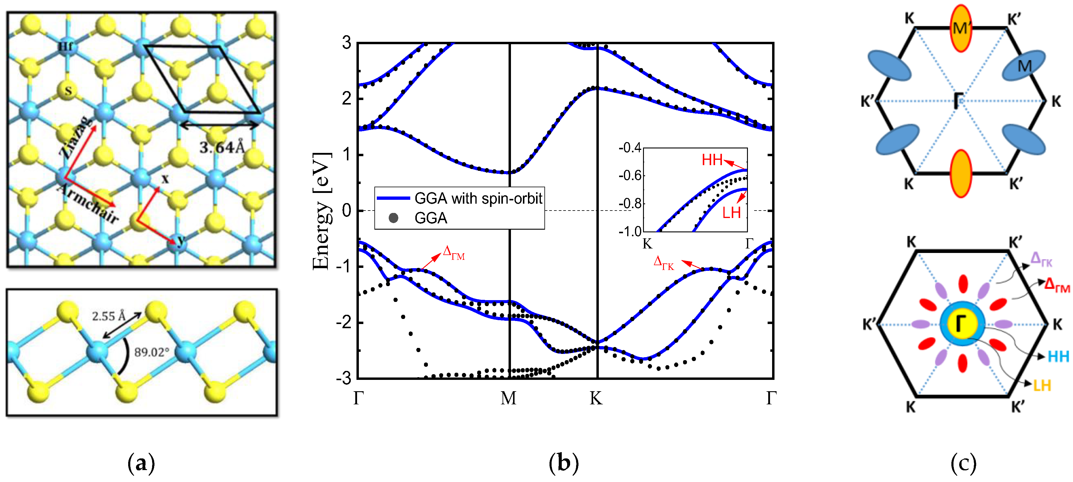
Figure 2.
Energy contour plots for (a) M’ valley, (b) M valley, (c) HH band, and (d) LH band of monolayer HfS2. Note that M’ and M valleys are CB while HH and LH bands are VB. Here Energy contour plots is based on ab-initio band structure calculation using GGA with spin-orbit coupling. Dash lines are calculated results from compact band models including Rudenko model and new compact model.
Figure 2.
Energy contour plots for (a) M’ valley, (b) M valley, (c) HH band, and (d) LH band of monolayer HfS2. Note that M’ and M valleys are CB while HH and LH bands are VB. Here Energy contour plots is based on ab-initio band structure calculation using GGA with spin-orbit coupling. Dash lines are calculated results from compact band models including Rudenko model and new compact model.
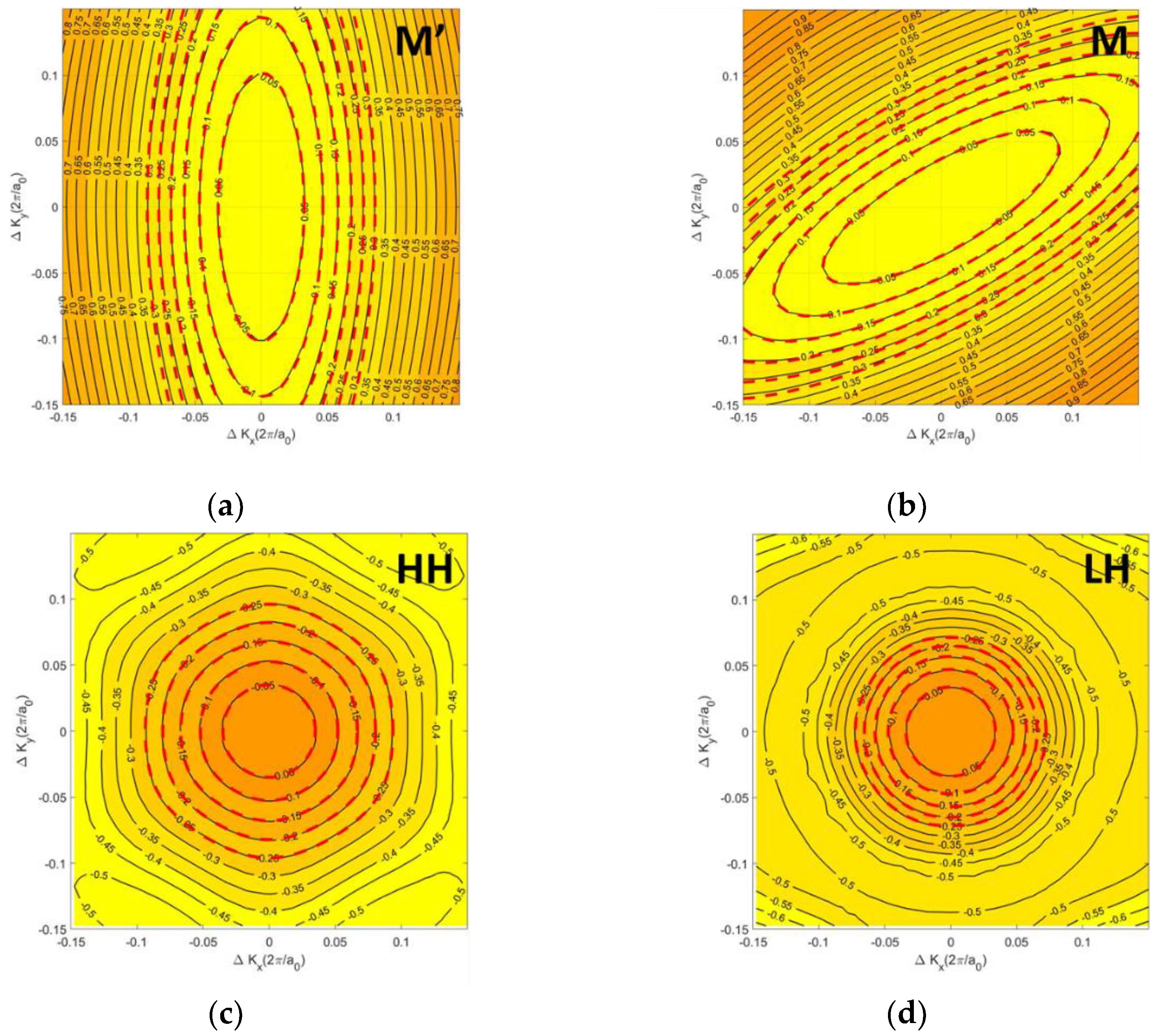
Figure 3.
(a) Density of states and (b) velocity square as a function energy for M’ valley of monolayer HfS2, respectively. (c) Density of states and (d) velocity square as a function energy for valence band of monolayer HfS2, respectively. Above calculations are based on ab-initio GGA band structure.
Figure 3.
(a) Density of states and (b) velocity square as a function energy for M’ valley of monolayer HfS2, respectively. (c) Density of states and (d) velocity square as a function energy for valence band of monolayer HfS2, respectively. Above calculations are based on ab-initio GGA band structure.
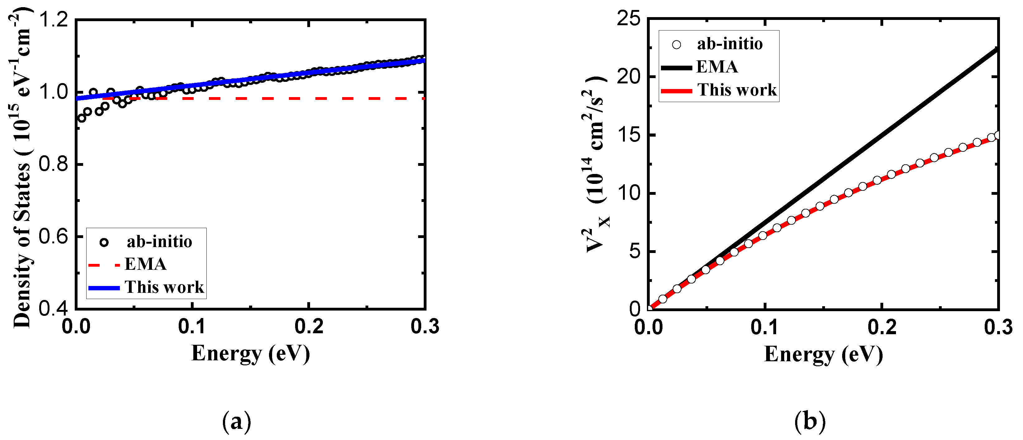
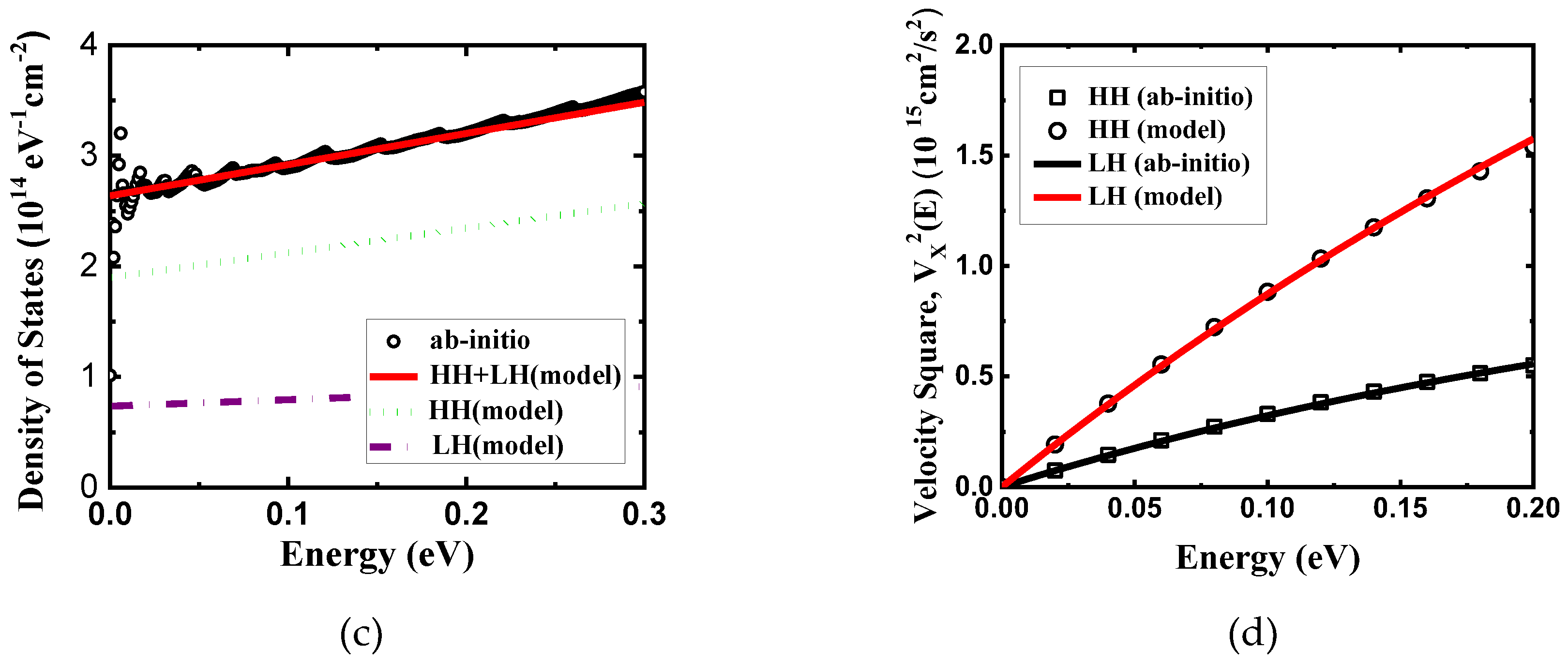
Figure 4.
Key parameters including (a) effective mass and (b) non-parabolicity factor of Rudenko model for conduction band of monolayer HfS2 under biaxial strain. Key parameters including (c) effective mass and (d) non-parabolicity factor of new compact model for valence band HH of monolayer HfS2 under biaxial strain. Key parameters including (e) effective mass and (f) non-parabolicity factor of new compact model for valence band LH of monolayer HfS2 under biaxial strain.
Figure 4.
Key parameters including (a) effective mass and (b) non-parabolicity factor of Rudenko model for conduction band of monolayer HfS2 under biaxial strain. Key parameters including (c) effective mass and (d) non-parabolicity factor of new compact model for valence band HH of monolayer HfS2 under biaxial strain. Key parameters including (e) effective mass and (f) non-parabolicity factor of new compact model for valence band LH of monolayer HfS2 under biaxial strain.
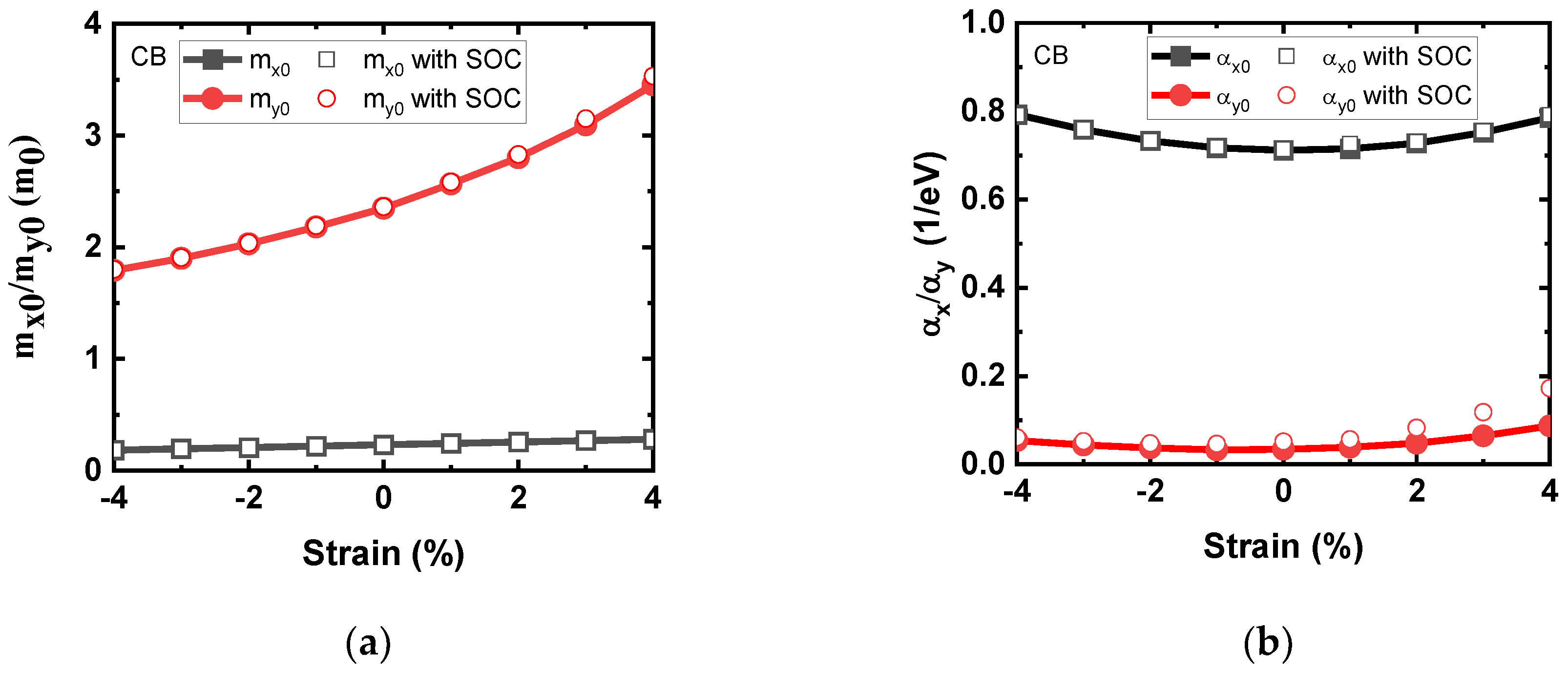
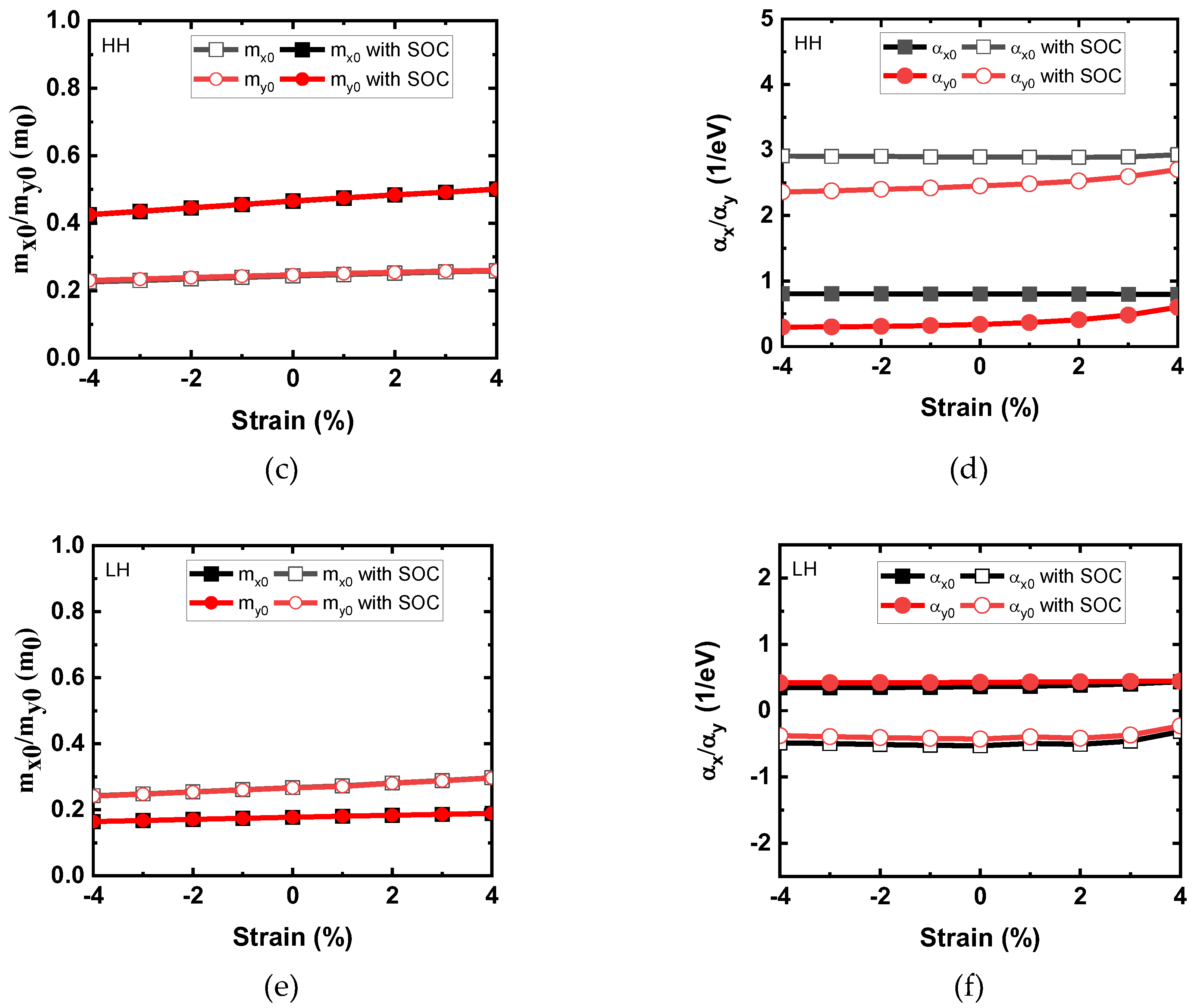
Figure 5.
The change of (a) lowest conduction band and (b) top two highest valence band of monolayer HfS2 under compressive and tensile biaxial strains as calculated by ab-initio method with GGA considering SOC.
Figure 5.
The change of (a) lowest conduction band and (b) top two highest valence band of monolayer HfS2 under compressive and tensile biaxial strains as calculated by ab-initio method with GGA considering SOC.
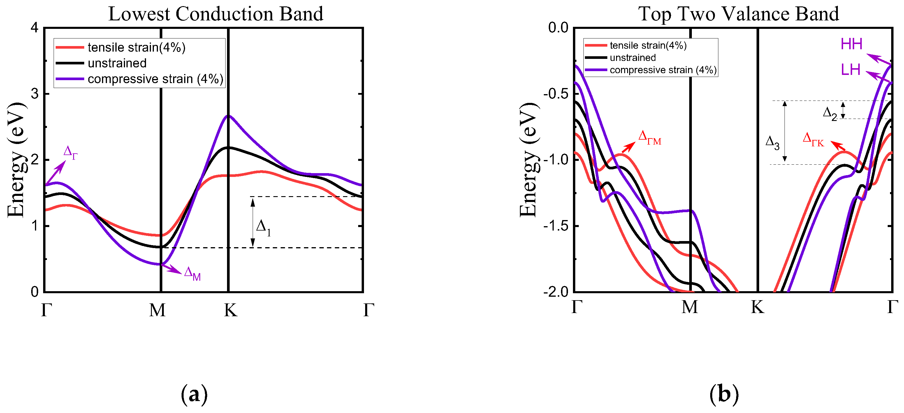
Figure 6.
(a) The variation of bandgap of monolayer HfS2 under biaxial strain. (b) Absolute conduction band edge (Ec) and valence band edge (Ev) for ab-initio calculations with GGA considering SOC or not as a function of biaxial strain. (c) Energy difference between conduction band (△1) and valence band valleys (△2 and △3) versus biaxial strain.
Figure 6.
(a) The variation of bandgap of monolayer HfS2 under biaxial strain. (b) Absolute conduction band edge (Ec) and valence band edge (Ev) for ab-initio calculations with GGA considering SOC or not as a function of biaxial strain. (c) Energy difference between conduction band (△1) and valence band valleys (△2 and △3) versus biaxial strain.
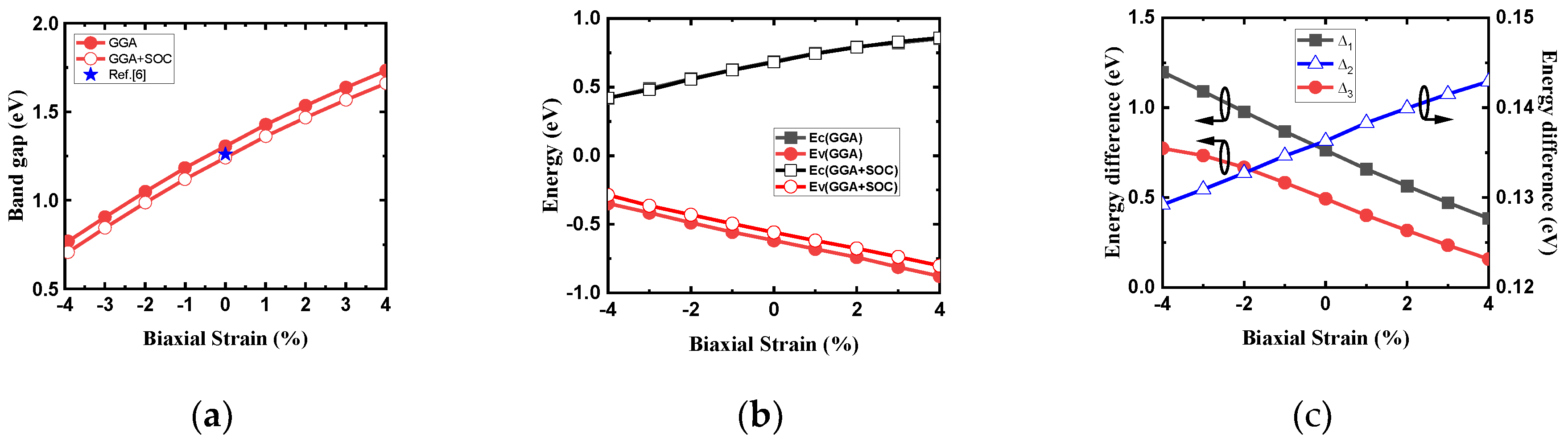
Figure 7.
(a) Phonon-limited electron mobility without polar optical phonon scattering versus electron density with two compact band models for monolayer HfS2. (b) Electron mobility with polar optical phonon scattering as a function of electron density. Square symbol is imec’s calculated data from Ref. [6].
Figure 7.
(a) Phonon-limited electron mobility without polar optical phonon scattering versus electron density with two compact band models for monolayer HfS2. (b) Electron mobility with polar optical phonon scattering as a function of electron density. Square symbol is imec’s calculated data from Ref. [6].
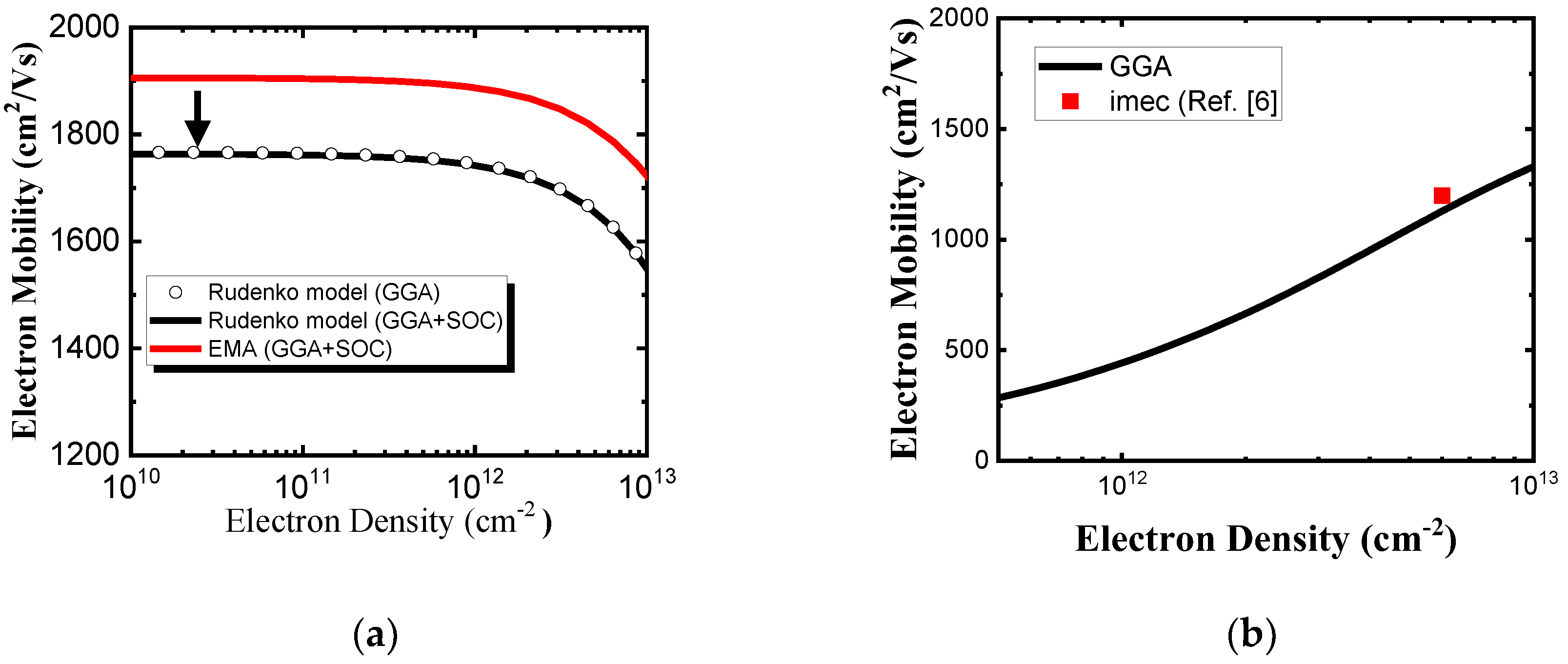
Figure 8.
(a) Electron mobility change ratio as a function of biaxial strain. (b) Enhancement factors ( and ) versus biaxial strain.
Figure 8.
(a) Electron mobility change ratio as a function of biaxial strain. (b) Enhancement factors ( and ) versus biaxial strain.
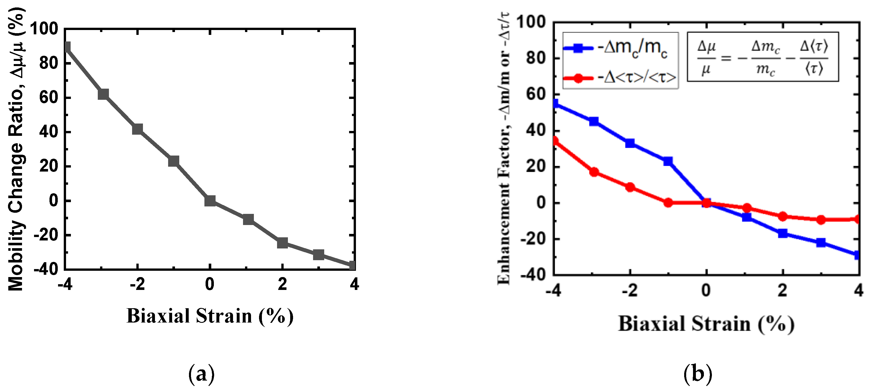
Figure 9.
(a) Phonon-limited hole mobility without polar optical phonon scattering versus hole density with two compact band models for monolayer HfS2. (b) Hole mobility with polar optical phonon scattering as a function of hole density. Square symbol is imec’s calculated data from Ref. [6].
Figure 9.
(a) Phonon-limited hole mobility without polar optical phonon scattering versus hole density with two compact band models for monolayer HfS2. (b) Hole mobility with polar optical phonon scattering as a function of hole density. Square symbol is imec’s calculated data from Ref. [6].
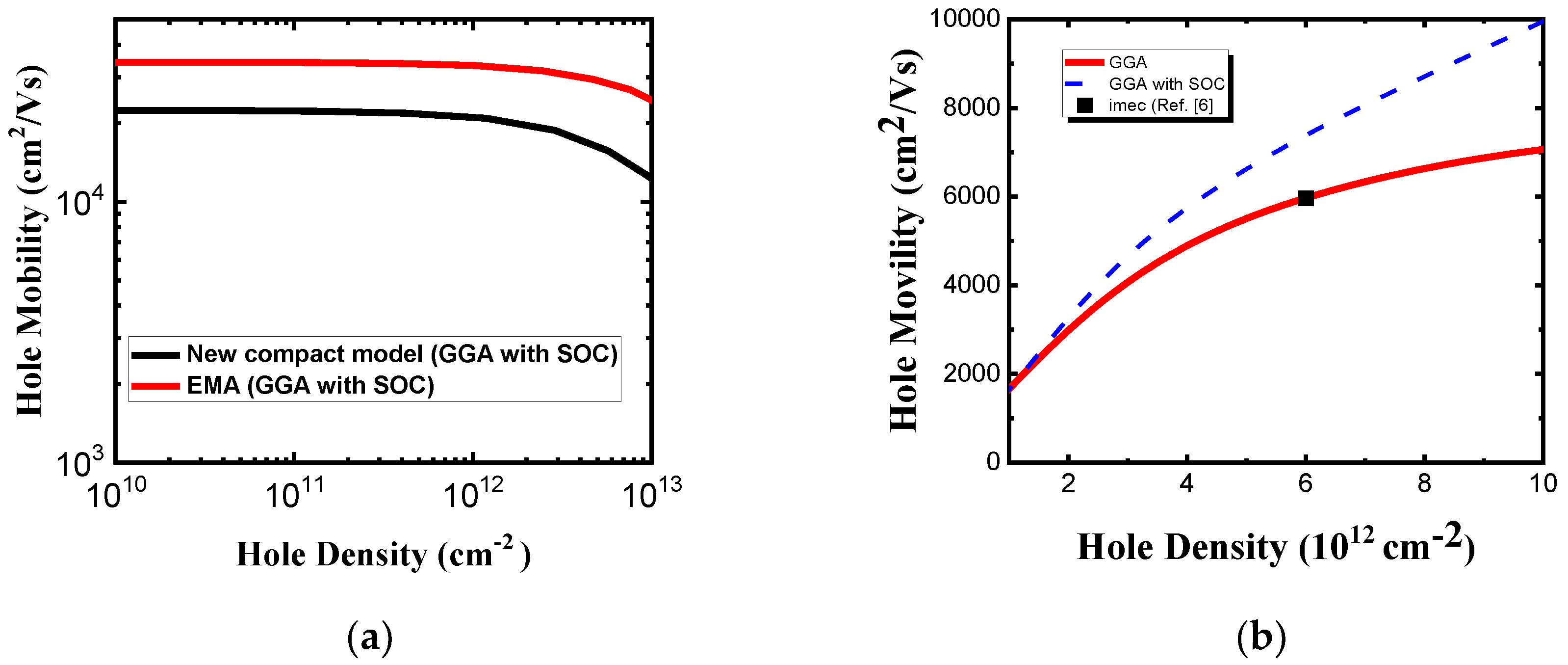
Figure 10.
(a) Hole mobility change ratio as a function of biaxial strain. (b) Enhancement factors ( and )versus biaxial strain.
Figure 10.
(a) Hole mobility change ratio as a function of biaxial strain. (b) Enhancement factors ( and )versus biaxial strain.
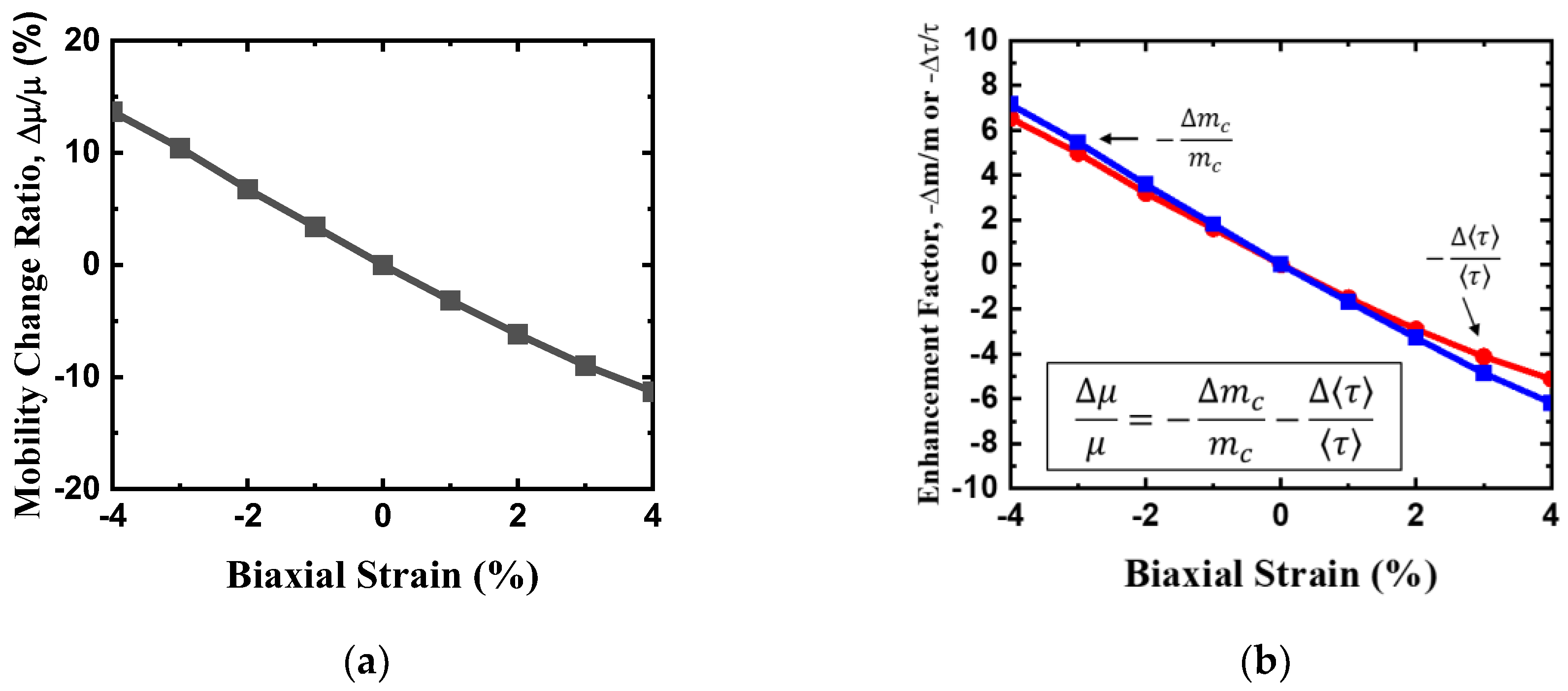

Table 1.
The effective mass for CB and VB of monolayer HfS2 by ab-initio calculation with GGA and GGA+SOC, respectively.
Table 1.
The effective mass for CB and VB of monolayer HfS2 by ab-initio calculation with GGA and GGA+SOC, respectively.
| GGA | |||
| Valley/band | mMГ/mAR (m0) | mMK/mZA(m0) | mDOS=(mMГmMK)1/2 (m0) |
| M’ valley | 2.36 | 0.23 | 0.74 |
| M valley | 0.3 | 0.71 | 0.74 |
| mГM (m0) | mGK (m0) | mDOS = (mГMmГK)1/2(m0) | |
| HH band | 0.47 | 0.47 | 0.47 |
| LH band | 0.18 | 0.18 | 0.18 |
| GGA+SOC | |||
| Valley/band | mMГ/mAR (m0) | mMK/mZA(m0) | mDOS=(mMГmMK)1/2 (m0) |
| M’ valley | 2.35 | 0.23 | 0.74 |
| M valley | 0.3 | 0.71 | 0.74 |
| mГM (m0) | mGK (m0) | mDOS = (mГMmГK)1/2(m0) | |
| HH band | 0.25 | 0.24 | 0.24 |
| LH band | 0.27 | 0.27 | 0.27 |
Table 2.
The new compact model parameters for CB of monolayer HfS2.
| GGA | ||
| GGA+SOC | ||
Table 3.
The new compact model parameters for HH/LH VB of monolayer HfS2.
| GGA | ||
| HH/LH | HH/LH | |
| GGA+SOC | ||
| HH/LH | HH/LH | |
Table 4.
The effective mass, deformation potential constant of electron and hole for unstrained monolayer HfS2 by ab-initio calculation with GGA.
Table 4.
The effective mass, deformation potential constant of electron and hole for unstrained monolayer HfS2 by ab-initio calculation with GGA.
| Carriers | mMГ/mHH (m0) | mMK/mLH (m0) | Dac (eV) | Dop (108eV/cm) |
| electron | 2.36 | 0.23 | 1.31 | 0.99 |
| hole | 0.47 | 0.18 | 0.95 | 0.73 |
Disclaimer/Publisher’s Note: The statements, opinions and data contained in all publications are solely those of the individual author(s) and contributor(s) and not of MDPI and/or the editor(s). MDPI and/or the editor(s) disclaim responsibility for any injury to people or property resulting from any ideas, methods, instructions or products referred to in the content. |
© 2024 by the authors. Licensee MDPI, Basel, Switzerland. This article is an open access article distributed under the terms and conditions of the Creative Commons Attribution (CC BY) license (http://creativecommons.org/licenses/by/4.0/).
Copyright: This open access article is published under a Creative Commons CC BY 4.0 license, which permit the free download, distribution, and reuse, provided that the author and preprint are cited in any reuse.


