
Submitted:
10 January 2025
Posted:
10 January 2025
You are already at the latest version
Abstract
The phase transition of MAPbI3 during the annealing process has been extensively reported, but there is a lack of research on the preformation of resulting perovskite solar cells (PSCs). Here, we systematically investigated the impact of annealing temperature on the crystal structure of MAPbI3. Our findings reveal that an optimal annealing temperature of 100°C yields high crystallinity and a mixture of tetragonal and cubic phases. Deviating from this temperature range results in incomplete conversion to perovskite material at lower temperatures or formation of only cubic crystal structure above 100°C, leading to degradation at higher temperatures. Theoretical calculations also indicate that the conduction band energy level for the cubic phase is approximately 154 meV lower than that for the tetragonal phase, creating an electron extraction barrier between perovskite and TiO2. Solar cells fabricated with mixed-phase films annealed at 100°C exhibit superior performance with a conversion efficiency of 22.01%, attributed to both energetically favourable crystal structure and excellent crystallinity.
Keywords:
perovskite solar cells
; phase transition
; morphology
; methylammonium lead halide
; annealing temperature
Perovskite solar cells (PSCs) have attracted significant attention due to their impressive efficiency achieved using cost-effective and low-temperature solution-processing methods.[1,2,3,4,5,6,7,8,9] In a PSC, the perovskite material absorbs photons and then generates electron-hole pairs in the material. Methylammonium lead halide (MAPbI3), most widely studied perovskite absorber, is a temperature sensitive material due to the phase transition and thermal decomposition that can occur during the annealing process.[10] There are two approaches to deposit the MAPbX3 perovskite light absorbing film: a one-step method where a precursor solution containing PbX2 and MAX in organic solvent is used for the film deposition [11] and two-step method where the PbX2 and MAX precursors are deposited separately to form the MAPbX3 compound.[12] An annealing step following the film deposition is generally required to remove the organic solvent and to crystallize the perovskite film.[13]
Crystallographically, the perovskite MAPbI3 can exist in three crystalline phases: cubic; tetragonal; and orthorhombic. The phase transition occurs at relatively low temperatures (55°C for tetragonal to cubic) [14,15] The phase transition may also be related to the different interface between the organic and inorganic components. The CH3NH3I and PbI2 components in the compound interact through hydrogen bonding between the amino group and the halide ions, whereas the weak Van der Waals interactions exists among the organic components. Since phase transformation of MAPbI3 films is expected to influence on performance of corresponding solar cells,[16] an in-depth understanding the correlation between the material structure of MAPbI3 and the performance of PSC is important to optimize the experimental conditions for improving the device efficiency.
To give an insight into correlation of the component of MAPbI3 with the performances of PSC, here we present a study on the effect of different crystal structure and the morphology induced by the annealing temperature and the performance of corresponding solar cells. Theoretical calculations based on density function theory (DFT) were also undertaken to determine the relative energy levels and bandgap of different MAPbI3 crystal structures. The lower conduction band of the MAPbI3 cubic phase relative to that of TiO2 results in unfavored charge transfer from the perovskite light absorber to TiO2, leading to a lower energy conversion efficiency of the PSC.
Experiment
First, laser-patterned, FTO-coated glass substrates (Tec15) were cleaned by ultra-sonication in an alkaline, aqueous washing solution, rinsed with deionized water, ethanol and acetone, and heated to 510oC to remove the residual organic material. An 80 nm-thick TiO2 compact layer was then deposited on the substrates by aerosol spray pyrolysis at 500oC using a commercial titanium diisopropoxide bis(acetylacetonate) solution (75% in 2-propanol, Sigma-Aldrich) diluted in ethanol (0.2 mol/L). After cooling to room temperature, the substrates were treated in 0.05 M aqueous solution of TiCl4 for 30 min at 70 oC, rinsed with deionized water and dried at 500oC for 20 min. The mesoporous TiO2 layer composed of 20 nm sized particles was deposited by spin coating at 5000 rpm for 30 s using a commercial TiO2 paste (Dyesol 18NRT) diluted in ethanol (2:7, weight ratio). The TiO2 films were gradually heated to 510℃, baked at this temperature for 15 min and cooled to room temperature. Prior to their use, the films were again dried at 500oC for 30 min.
The deposition of perovskite materials and PSC device fabrication were carried out in an Ar-filled glove box with oxygen content<0.1 ppm, H2O content < 0.1 ppm. PbI2 was dissolved in N,N-dimethylformamide at a concentration of 462 mg/ml under stirring at 70oC. The solution was kept at 70oC during the whole procedure. The mesoporous TiO2 films were then infiltrated with PbI2 by spin coating at 6500 r.p.m. for 90 s and dried at 70oC for 30 min. After cooling to room temperature, the films were dipped in a solution of CH3NH3I in 2-propanol (10 mg/ml) for 20 s, rinsed with 2-propanol and dried at different temperatures (50oC, 70oC, 100oC, 120oC and 140oC) for 30 min. The hole transfer material (HTM) was then deposited by spin coating at 4000 r.p.m. for 30 s. The spin coating formulation was prepared by mixing 72.3 mg 2,29,7,79-tetrakis(N,N-di-p-methoxyphenylamine)-9,9-spirobifluorene (spiro-MeOTAD), 28.8 ml 4-tert-butylpyridine, 17.5 ml of a stock solution (520 mg/ml lithium bis(trifluoromethylsulphonyl)imide in acetonitrile) and 1 ml chlorobenzene. Finally, 80 nm of gold film with geometry of 4 mm × 4 mm was thermally evaporated on top of the device to form the back contact.
The UV-visible spectrum and diffuse reflectance spectroscopy of the material were recorded on a UV-Vis spectrometer with an integrating sphere (Cary 5000). The surface and cross-section morphology of the MAPbI3 films were imaged using a field emission scanning electron microscope (FESEM, JEOL 7001F) at an acceleration voltage of 10.0 kV. The high resolution transmission electron microscope (HRTEM) measurement and selected area electron diffraction patterns of the HTM composite were performed with a JEOL 2010 transmission electron microscope with an accelerating voltage of 200 keV. Electron microprobe (JEOL JXA-8530F) was used to measure the atomic percentage of the film in the condition of 7 kV, 20 nA, probe diameter is 5 µm. The data has been analysed by Electron probe micro-analyser. The photocurrent density-voltage (J-V) plots of the solar cells were measured by recording the current as a function of applied voltage under the radiation of 100 mW/cm2 (AM1.5) provided by a Xe lamp (150 W) based solar simulator (Newport). The cell was scanned from short circuit to open circuit. The illumination intensity of the solar simulator was calibrated with a monocrystalline reference silicon solar cell (Fraunhofer ISA). The active area of 0.09 cm2 of each cell was controlled using a black mask (3 mm ×3 mm) which was placed opposite to the gold contact.
Result and discussion
Figure 1 shows the SEM images of the deposited MAPbI3 films annealed at different temperatures. The SEM image of the film annealed at 50oC is obscure, it is most likely caused by the poor conductivity and crystallinity of the films arising from the the low annealing temperature, which could not fully convert the PbI2 into CH3NH3PbI3 perovskite crystal (Figure 1a). In contrast, a clear and smooth homogeneous surface consisting of nanoparticles is observed with the sample annealed at 70ºC (Figure 1b), and the film annealed at 100ºC shows a surface consisting of compact grains which closely connect with each other (Figure 1c). Annealing the film above 100oC, such as 120oC and 140oC (Figure 1d and 1e, respectively), leads to the formation of nano-sheets of perovksite.
To further study the evolution of the crystal structure and crystallinity of the MAPbI3 films annealed at different temperatures, high resolution transmission electron microscopy (HRTEM) (Figure 2) and selected area electron diffraction (SAED) pattern (inset) were employed. Figure 2a shows the HRTEM image of the MAPbI3 film annealed at 50oC, the lattice fringes with a separation of 0.28 nm matches the inter-planar spacing of the (114) plane of tetragonal MAPbI3 structure, while the lattice fringes at 0.18 nm is attributed to the inter-planar spacing of the (023) plane of PbI2 (PDF ref. code: 96-900-9141), indicating that the MAPbI3 film annealed at 50oC contains both tetragonal MAPbI3 and a small amount of unreacted PbI2. For the film annealed at 70oC (Figure 2b), the lattice spacings of 0.31 nm and 0.25 nm are assigned to the (220) and (024) space planes of tetragonal phase of MAPbI3,[17] The lattice fringe spacing of 0.34 nm is assigned to the (100) plane of cubic MAPbI3,[18] inferring that the 70oC deliver the mixture phase of tetragonal and cubic crystal of MAPbI3. A Similar mixture of crystal structures is also found while annealing the perovskite film at 100oC, while the perovskite high crystalline from the SEAD results (Figure 2c). Increasing the annealing temperature to 120oC, only a lattice fringe spacing of 0.34 nm was found, which is due to (100) plane of the cubic structure (Figure 2d). Figure 2e shows the HRTEM image of perovskite film annealed at 140oC, a clear lattice space 0.233 nm which is attributed to (006) lattice plane of PbI2 was observed. The SEAD patterns from (006), (016) and (027) lattice plane of PbI2 are also observed, confirming the existence of PbI2, this could be due to the decomposition of perovskite film at higher temperature.
Combining the SEM and HRTEM results, we deduce that the perovskite film annealed at low temperature (50oC, 70oC) has poor crystallinity, and especially at 50oC, the precursor of PbI2/CH3NH3I has not been fully converted into CH3NH3PbI3. At 70oC, the perovskite films shows evidence of two crystal structures, tetragonal and cubic phase. Increasing the annealing temperature of perovskite layer to 100oC, the perovskite film also shows two crystal structures, but the crystallinity of the MAPbI3 material is significantly improved, and a dense and high crystallinity of perovskite film has been formed. However, further increasing the temperature to 120oC, although the film still shows high crystallinity, nano-sheets of perovskite film has been formed, the film contained a lot of pinholes, which will not be good for the device performance. By further increasing the annealing temperature to 140oC, the perovskite was further degraded into PbI2.
The absorption properties of the perovskite films were studied by the UV-vis absorption spectra. From Figure 3a, it is found that the absorption peak intensities increase with annealing temperature until 100oC, further increasing of the annealing temperature to 120oC leads to the decrease of light absorption intensity of the film. Under lower annealing temperature, the film absorption increase could be due to increased perovskite crystal formation and also the increase crystallinity, while reduced the absorption is likely due to the degradation of the perovskite layer.
The optical bandgap of the MAPbI3 film annealed at different temperatures can be determined (Figure 3b) using the transformed diffuse reflectance technique according to the well-known Kubelka-Munk theory. [19] The bandgap, Eg, can be obtained by regression fitting the linear part of the plot to the axis of the abscissa. The bandgap of the MAPbI3 films annealed at 50oC, 70oC, 100oC, 120oC and 140oC are 1.59 eV, 1.57 eV, 1.56 eV, 1.54 eV, and 1.52 eV, respectively, which fall in the range of bandgap of MAPbX3 (1.5~1.65 eV) reported in literature.[20] It is found that the bandgap decreases with the increase of the cubic phase in the material as the annealing temperature increases. This trend is consistent with the theoretical predication. [21]
To explain why the perovskite bandgap shifts while annealing the perovskite film under different temperature, density functional theory (DFT) calculations using the projector augmented wave method with the PBE exchange correlation function implemented in the plane-wave basis Vienna Ab-initio Simulation Package (VASP) code.[22] A damped van der Waals correction is incorporated based on Grimme’s scheme to account for the non-bonding interaction. The energy cut-off for plane waves is chosen to be 500 eV and the convergence of tolerance force on each atom during geometry optimization is set to 0.005 eV/Å. In Figure 4, we present the calculated band structures for the cubic and tetragonal polymorphs of MAPbI3, respectively.
The cubic phase has a well-defined direct band gap, Eg, of 1.445 eV at the E point (Figure 4a). Compared to the Eg determined by the Kubelka–Munk plot (1.54 eV), the slightly lower Eg value is attributed to the defects in the bulk film. The tetragonal phase with the tilted PbI6 octahedron around the c axis will move the band to the Γ point due to the lowering of the lattice symmetry and the band gap is slightly increased to 1.580 eV (Figure 4b). The above theoretical results are in good agreement with existing theoretical and experimental value[23].
The calculated electronic energetic properties of different crystal MAPbI3 phases are summarized in Figure 4c. Comparing with the tetragonal phase of MAPbI3, the cubic phase band has been shifted down about 0.15 eV. Considering that the conduction band (Ec) of MAPbI3 with tetragonal structure is only 0.07 eV higher than that of TiO2 which provides the driving force for electron extraction,[24] the deeper EC of the cubic phase compared to the tetragonal means that the electron extraction from the perovskite material to TiO2 is not very energetically for the solar cell based on the MAPbI3 film annealed at 120oC.
The representative photocurrent density-voltage (J-V) plots of the solar cells using MAPbI3 films annealed at different temperature are shown in Figure 4d. It is obviously that annealed at 100oC showed the highest cell efficiency (22.01%). The cells based on the film annealed at 50oC, 70oC and 120oC produced conversion efficiency of 15.73%, 18.03% and 12.14%, respectively. In contrast, further increase the annealing temperature to 140oC damaged the device with efficiency only 5.02% and short circuit current density (Jsc) of 9.35 mA/cm2. The drastic decrease of the cell performance should be due to the decomposition of the MAPbI3 thin films.[25] The detailed device performance for the perovskite annealing at different temperature are summarized in Table 1.While the annealing temperature increasing from 50oC to 100oC, it can be seen the open circuit voltage (Voc) clearly increase, indicating that charge recombination has been reduced as the crystallinity improves. While further increasing of the temperature led to a decrease of the Voc, and a massive reduction in the fill factor, most likely due to the increasing porosity of the large crystals leading to increased resistance. PSCs annealed upon 100oC delivers the highest short circuit current. Theoretically Jsc of a perovskite solar cells is controlled by two critical processes: (1) the light harvesting efficiency of MAPbI3, and (2) the electron extraction efficiency which is controlled by the energy offset between MAPbI3 and TiO2. As illustrated in Figure 3a, the light absorption intensity of the perovskite films shows the absorption harvest efficiency is 100oC >120oC >70oC >50oC. Consistent with the absorption results, the 100oC annealed film showed the highest short circuit current. However, the Jsc of the perovskite film annealed at 120oC is significantly lower than that of the film annealed at 70oC, even though the former shows higher light absorption. This inconsistency between short circuit current and light harvesting efficiency could be due to the difference in charge extraction efficiency. As well known, the charge extraction efficiency is mainly controlled by the energy offset between the light absorber and TiO2, which provides the driving force for photo-generated electron injection. Since the energy driving force for electron injection from tetragonal MAPbI3 to TiO2 is only around 0.07 eV,[24] the Ecb of cubic phase MAPbI3 is 0.15 eV lower than tetragonal counterpart means that the conduction band of cubic MAPbI3 is lower (more positive) than the Ecb of TiO2. This unfavorable energy band alignment means that electron charge extraction from the cubic MAPbI3 to TiO2 is not favorable. Therefore, the loss of charge transport pathway via TiO2 is mainly responsible for the lower Jsc of the sample annealed at 120oC.
Conclusion
In conclusion, the effects of annealing temperature on the crystal structure and crystallinity of MAPbI3 film as well as on the corresponding solar cell performances have been systematically investigated. It has been found that the film annealed at low temperature showed poor crystallinity with tetragonal crystal structure, and the perovskite film contained un-reacted PbI2. The tetragonal and cubic mixed crystal structure are both found whiling annealing the perovskite at 70ºC, 100ºC. Higher temperature annealing will lead to the nanoplate crystallinity or the decomposition of perovskite. Theoretical calculation based on DFT simulation has predicted the conduction band of the cubic structure is energetically unfavorable for charge injection from the perovskite material to TiO2, which is responsible for the reduced performance of the solar cell with the film annealed at higher temperature. The highest performance was obtained while annealing the perovskite at a temperature (100oC) due to the better crystallinity and favourable crystal structure, as well as the suitable composition. These results will provide new insights into the correlations of properties of halide perovskite with the performance of solar cells, which will be helpful for fabricating highly efficiency PSCs.
Acknowledgments
This work was sponsored by the Special Foundation for Carbon Peak Carbon Neutralization Technology Innovation Program of Jiangsu Province (BE2022026), the National Natural Science Foundation of China (52202169, 22279033, and 62104253), the 111 Project (B16016), the Project for Young Foreign Experts (QN2023124001L).
References
- Kojima A, Teshima K, Shirai Y et al. Organometal halide perovskites as visible-light sensitizers for photovoltaic cells. 2009, J. Am. Chem. Soc. 131, 6050. [CrossRef]
- Kim H S, Lee C R, Im J H et al. Lead iodide perovskite sensitized all-solid-state submicron thin film mesoscopic solar cell with efficiency exceeding 9%. 2012, Sci. Rep. 2, 591.
- Drużbicki K, Gila-Herranz P, Marin-Villa P et al. Cation Dynamics as Structure Explorer in Hybrid Perovskites-The Case of MAPbI3. 2023, Cryst. Growth Des. 24, 1.
- Tan H, Jain A, Voznyy O et al. Efficient and stable solution-processed planar perovskite solar cells via contact passivation. 2017, Science 355, 722. [CrossRef]
- Yang W S, Park B W, Jung E H, et al. Iodide management in formamidinium-lead-halide-based perovskite layers for efficient solar cells. 2017, Science 356, 1376.
- Qiu J, McDowell L L, Shi Z. Room-Temperature Cubic Perovskite Thin Films by Three-Step All-Vapor Conversion from PbSe to MAPbI3. 2019, Cryst. Growth Des. 19, 3. [CrossRef]
- Kim G, Min H, Lee K S et al. Impact of strain relaxation on performance of α-formamidinium lead iodide perovskite solar cells. 2020, Science, 370, 108. [CrossRef]
- Li M, Yue Z, Ye Z et al. Improving the Efficiency and Stability of MAPbI3 Perovskite Solar Cells by Dipeptide Molecules. 2024, Small, 20, 2311400. [CrossRef]
- Lee S, Feldman J, Lee S. Nanoconfined Crystallization of MAPbI3 to Probe Crystal Evolution and Stability. 2016, Cryst. Growth Des. 16, 8.
- Jeon N J, Noh J H, Kim Y C et al. Solvent engineering for high-performance inorganic-organic hybrid perovskite solar cells. 2014, Nat. Mater. 13, 897.
- Liu N, Xiong J, Wang G et al. Overcoming the PCBM/Ag Interface Issues in Inverted Perovskite Solar Cells by Rhodamine-Functionalized Dodecahydro-Closo-Dodecaborate Derivate Interlayer. 2023, Adv. Funct. Mater. 33, 2300396. [CrossRef]
- Burschka J, Pellet N, Moon S J et al. Sequential deposition as a route to high-performance perovskite-sensitized solar cells. 2013, Nature, 499, 316. [CrossRef]
- Nguyen M H, Kim K S. Controlling the grain formation process with oleylamine and 4-dimethylaminopyridine additives for efficient and stable MAPbI3 solar cells. 2023, Mater. Today Chem. 34, 101799.
- Poglitsch A , Weber D. Dynamic disorder in methylammoniumtrihalogenoplumbates (II) observed by millimeter-wave spectroscopy. 1987, J. Chem. Phys. 87, 6373. [CrossRef]
- Kawamura Y, Mashiyama H, Hasebe K. Structural Study on Cubic-Tetragonal Transition of CH3NH3PbI3. 2002, J. Phys. Soc. Jpn. 71, 1694.
- Juarez-Perez E J, Wussler M, Fabregat-Santiago F et al. Role of the selective contacts in the performance of lead halide perovskite solar cells. 2014, J. Phys. Chem. Lett. 5, 680. [CrossRef]
- Wang J T, Ball J M, Barea E M et al. Low-Temperature Processed Electron Collection Layers of Graphene/TiO2 Nanocomposites in Thin Film Perovskite Solar Cells. 2014, Nano Lett. 14, 724.
- Gonzalez-Pedro V, Juarez-Perez E J, Arsyad W S et al. General Working Principles of CH3NH3PbX3 Perovskite Solar Cells. 2014, Nano Lett. 14, 888.
- Tauc J, Grigorovici R, Vancu A, Optical properties and electronic structure of amorphous germanium. 1966, Phys. Status Solidi. B, 15, 627.
- Noel N K, Stranks S D, Abate A et al. Lead-free organic-inorganic tin halide perovskites for photovoltaic applications. 2014, Energy & Environmental Science 7, 982. [CrossRef]
- Yin W J, Yang J H, Kang J et al. Halide perovskite materials for solar cells: a theoretical review. 2015, J. Mater. Chem. A. 3, 8926.
- Yang Y, Cai M L, Dai S Y et al. Dimension-controlled growth of antimony-based perovskite-like halides for lead-free and semitransparent photovoltaics. 2020, ACS Appl. Mater. Interfaces, 12, 17062.
- Matteocci F, Razza S, Giacomo F D et al. Solid-state solar modules based on mesoscopic organometal halide perovskite: a route towards the up-scaling process. 2014, PCCP, 16, 3918. [CrossRef]
- Quarti C, Grancini G, Mosconi E et al. The Raman Spectrum of the CH3NH3PbI3 Hybrid Perovskite: Interplay of Theory and Experiment. 2014, J. Phys. Chem. Lett. 5, 279.
- Dualeh A, Tétreault N, Moehl T et al. Effect of annealing temperature on film morphology of organic-inorganic hybrid pervoskite solid-state solar cells. 2014, Adv. Funct. 24, 3250. [CrossRef]
Figure 1.
Scanning electron microscopy (SEM) images of MAPbI3 film annealed at (a) 50ºC (b) 70ºC (c) 100ºC (d) 120ºC (e) 140ºC.
Figure 1.
Scanning electron microscopy (SEM) images of MAPbI3 film annealed at (a) 50ºC (b) 70ºC (c) 100ºC (d) 120ºC (e) 140ºC.
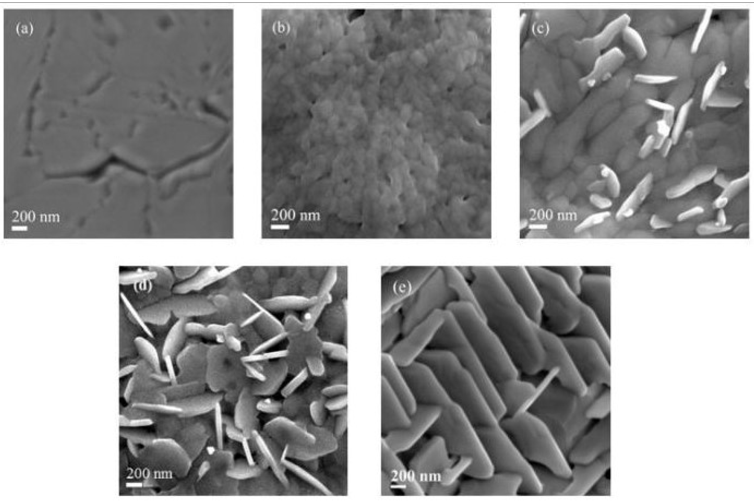
Figure 2.
High resolution transmission electron microscopy images (HRTEM) of MAPbI3 film annealed at (a) 50ºC (b) 70ºC (c) 100ºC (d) 120ºC (e) 140ºC. (Inset: corresponding selected area diffraction patterns of each sample).
Figure 2.
High resolution transmission electron microscopy images (HRTEM) of MAPbI3 film annealed at (a) 50ºC (b) 70ºC (c) 100ºC (d) 120ºC (e) 140ºC. (Inset: corresponding selected area diffraction patterns of each sample).
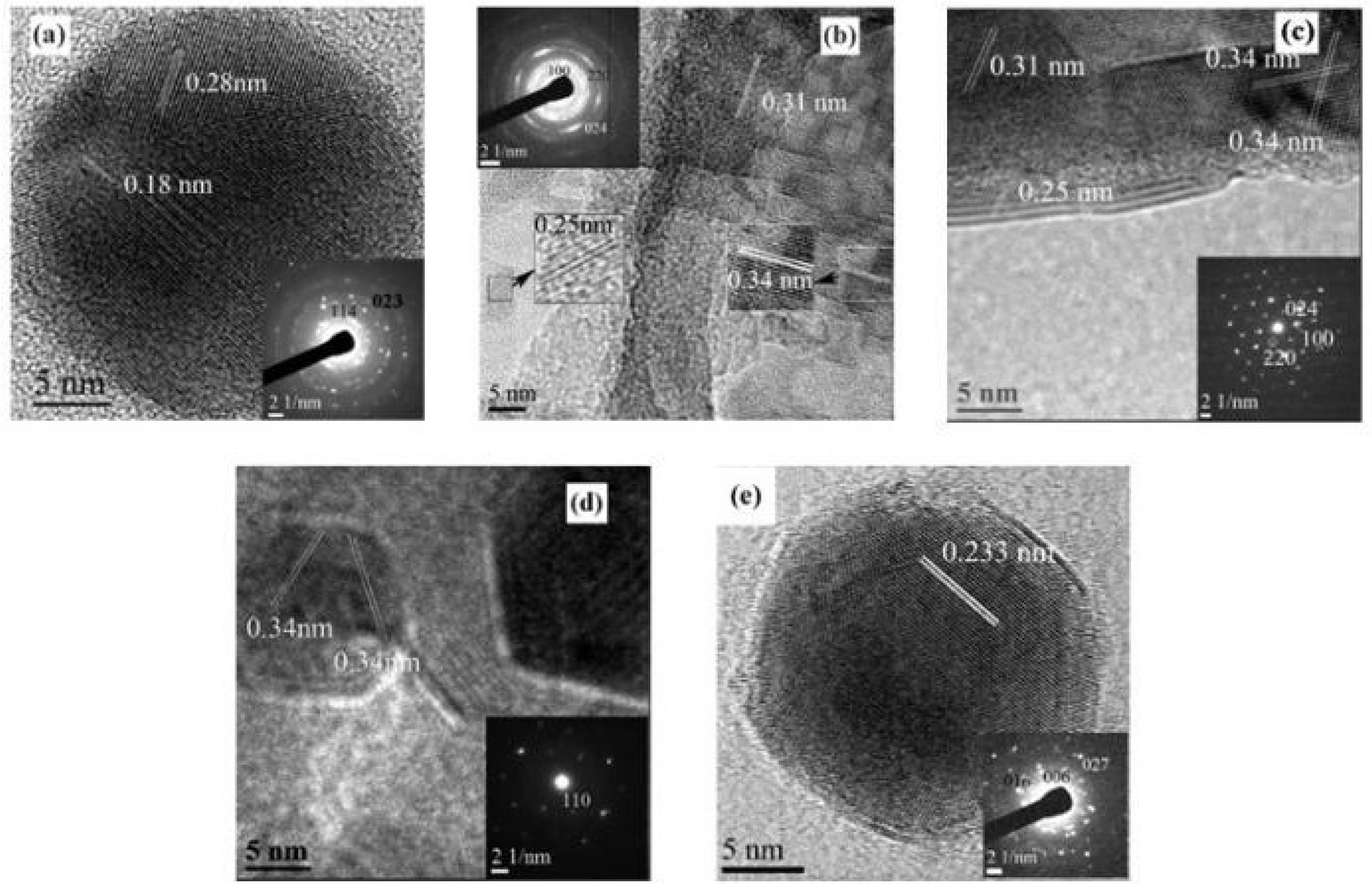
Figure 3.
(a) UV-vis absorption spectra of MAPbI3/TiO2 films and (b) converted Kubelka–Munk plots showing the bandgap of MAPbI3 film annealed at different temperatures.
Figure 3.
(a) UV-vis absorption spectra of MAPbI3/TiO2 films and (b) converted Kubelka–Munk plots showing the bandgap of MAPbI3 film annealed at different temperatures.
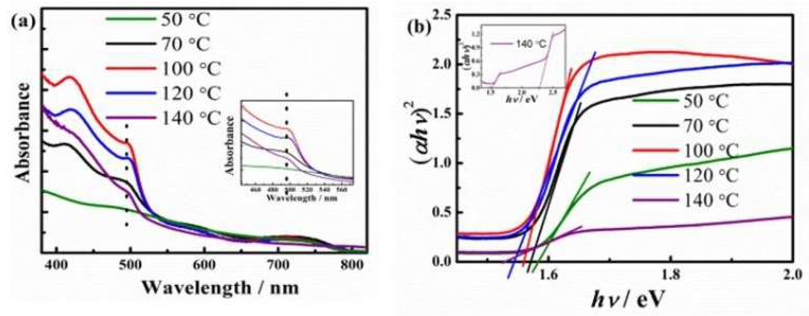
Figure 4.
Calculated band structures of MAPbI3 along the high-symmetry lines in the first Brillouin zone for the (a) cubic, (b) tetragonal, respectively. The Fermi level is set to zero. Calculated electronic energetic properties of two different crystal of MAPbI3. (c) The band alignment of TiO2 with tetragonal and cubic perovskite. (d) J-V plots of perovskite solar cells with MAPbI3 films annealed at different temperatures.
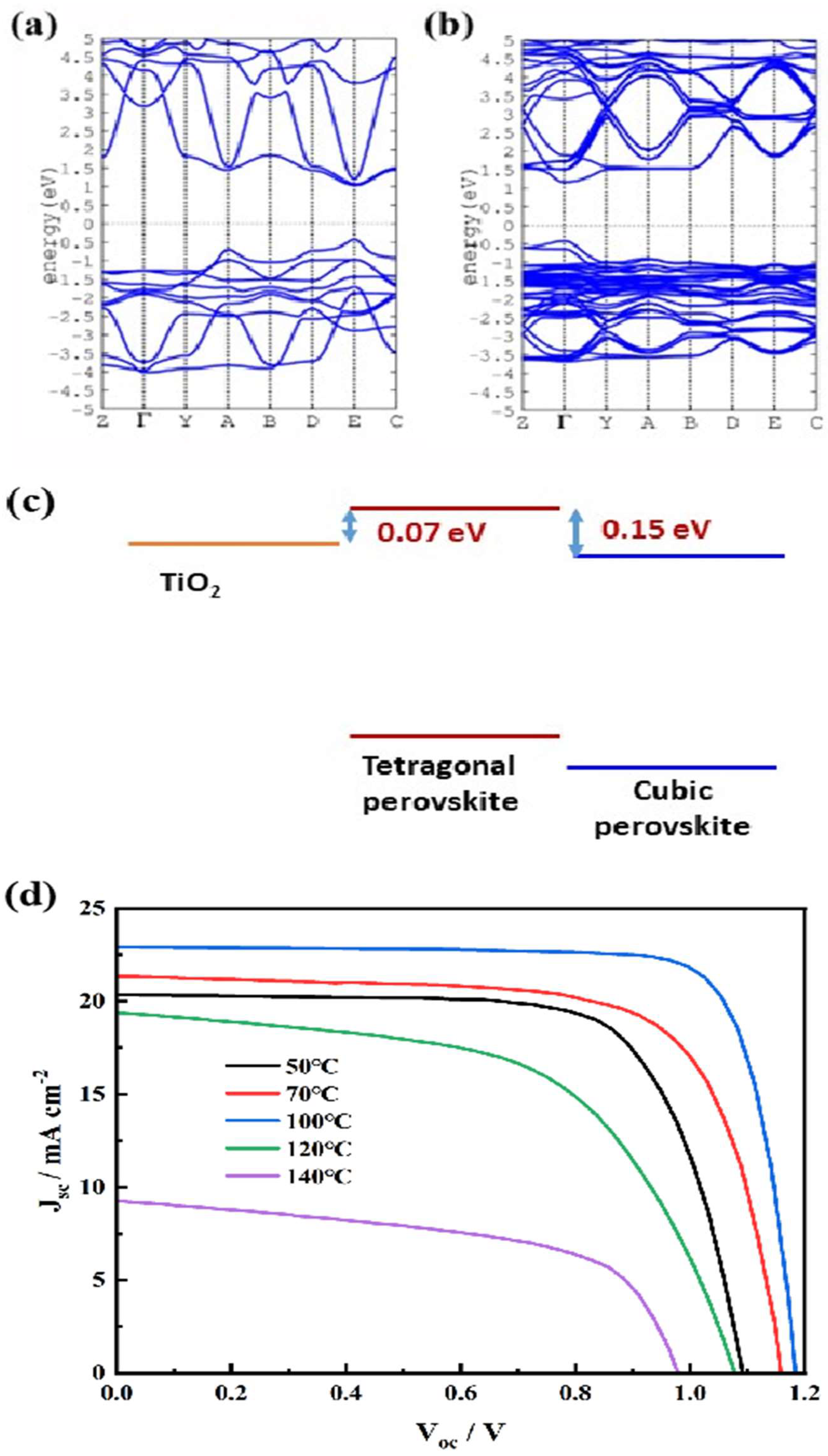

Table 1.
Photovoltaic parameters of perovskite solar cell based on MAPbI3 annealed at different temperatures.
Table 1.
Photovoltaic parameters of perovskite solar cell based on MAPbI3 annealed at different temperatures.
| Temperature (°C) |
Voc (V) | Jsc (mA cm-2) | FF | η (%) |
| 50 | 1.09 | 20.35 | 0.70 | 15.73 |
| 70 | 1.16 | 21.69 | 0.71 | 18.03 |
| 100 | 1.19 | 22.58 | 0.81 | 22.01 |
| 120 | 1.08 | 19.57 | 0.57 | 12.14 |
| 140 | 0.98 | 9.35 | 0.54 | 5.02 |
Disclaimer/Publisher’s Note: The statements, opinions and data contained in all publications are solely those of the individual author(s) and contributor(s) and not of MDPI and/or the editor(s). MDPI and/or the editor(s) disclaim responsibility for any injury to people or property resulting from any ideas, methods, instructions or products referred to in the content. |
© 2025 by the authors. Licensee MDPI, Basel, Switzerland. This article is an open access article distributed under the terms and conditions of the Creative Commons Attribution (CC BY) license (http://creativecommons.org/licenses/by/4.0/).
Copyright: This open access article is published under a Creative Commons CC BY 4.0 license, which permit the free download, distribution, and reuse, provided that the author and preprint are cited in any reuse.


