Preprint
Communication

This version is not peer-reviewed.

On-Chip Transformer Based Isolation Driver Chip Using PCB Technology

Ye Luo  *

Submitted:

08 January 2025

Posted:

08 January 2025

You are already at the latest version

Abstract

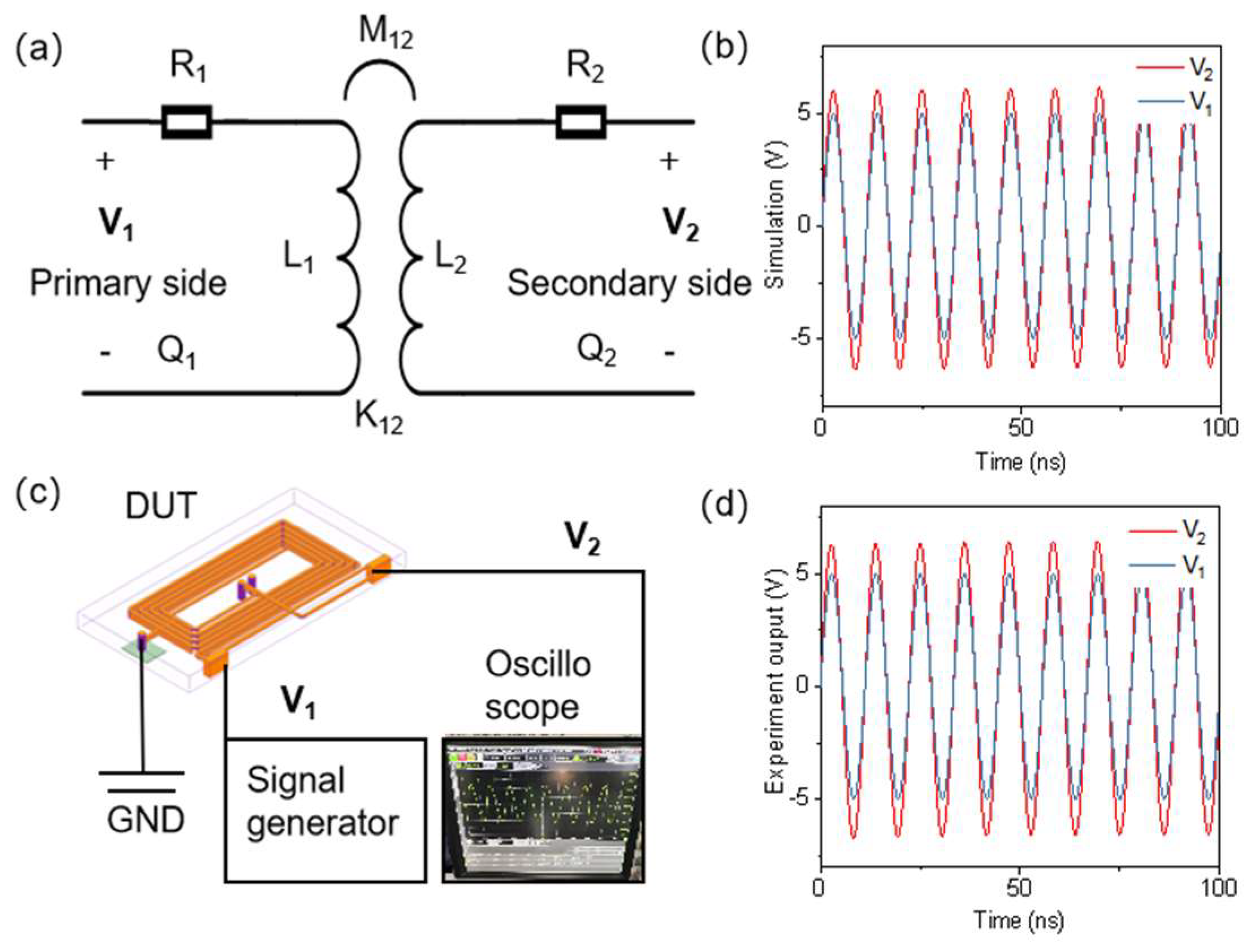
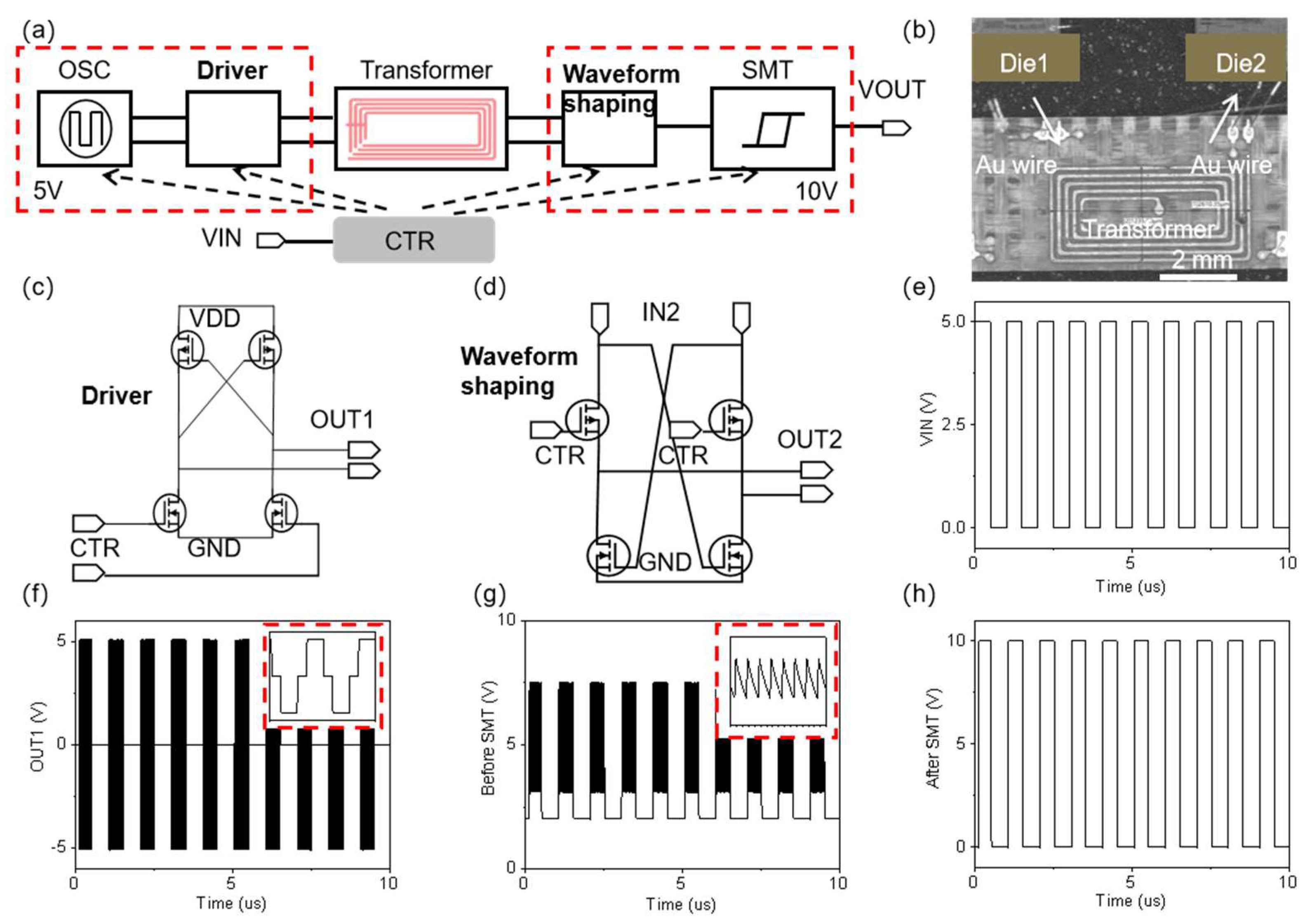
Isolation driver chips are widely used for reliable communication between low and high voltage levels, with on-chip transformers serving as the core devices for magnetic isolation. In this study, we designed, simulated, and tested an on-chip transformer that can be manufactured using PCB technology. This transformer uses copper as the conductive material and FR4 as the dielectric, theoretically achieving an insulation level of up to 3KV, making it suitable for mass production and showing significant industrial application potential. Based on this on-chip transformer, we designed corresponding encoding and decoding circuits and implemented the circuit structure through System in Package (SIP). Simulation results indicate that this isolation driver chip can reliably support communication across different voltage levels.

Keywords: 
;  ;  ;  

1. Introduction

Isolation driver chips are widely used in fields such as photovoltaic inverters [1], energy storage systems [2,3], electric drive system [4,5]. They effectively prevent voltage spikes and ground loops between low-voltage areas (e.g., microcontrollers) and high-voltage regions (e.g., gate drivers) through isolation shielding, ensuring reliable and safe communication between different voltage levels within a system [6-9]. The development of isolation driver chips primarily focuses on reducing manufacturing costs (such as processes, area, and packaging) while improving performance (such as power consumption, delay, and isolation level) [10,11]. Optocoupler typically require larger volumes [12,13], while capacitive isolator is mainly suitable for data communication [14,15]. In contrast, transformer based isolator is more suitable for power transmission, offering higher isolation levels, more compact integration, faster transmission speeds, and lower power consumption [16,17].
On-chip transformers (OCT) are key devices for achieving magnetic inductive coupling, and their development has received considerable attention [10,18]. Silicon-based OCTs have a dielectric breakdown strength of up to 850 V/µm but occupy a relatively large area [19]. Methods such as self-assembly are also research directions for on-chip transformers [20], while using mature Printed Circuit Board (PCB) technology can achieve both high isolation levels and low costs. Common Mode Transient Immunity (CMTI) is an important parameter for assessing isolation driver chips, referring to the ability of an isolator to maintain correct signal output during rapid voltage changes (dV/dt) [21]. This parameter is particularly crucial for rapidly switching power devices.
Therefore, this paper designs and manufactures an on-chip transformer compatible with PCB technology, incorporating a grounding shield layer to enhance CMTI, and designs a driver circuit based on this transformer. The wafer processing is completed under a fabless model, and the isolation driver function is realized through System in Package (SIP). This work primarily employs mature PCB and CMOS processes, demonstrating promising commercial prospects.

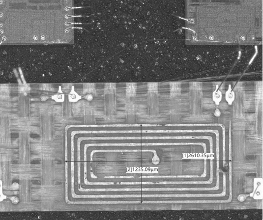
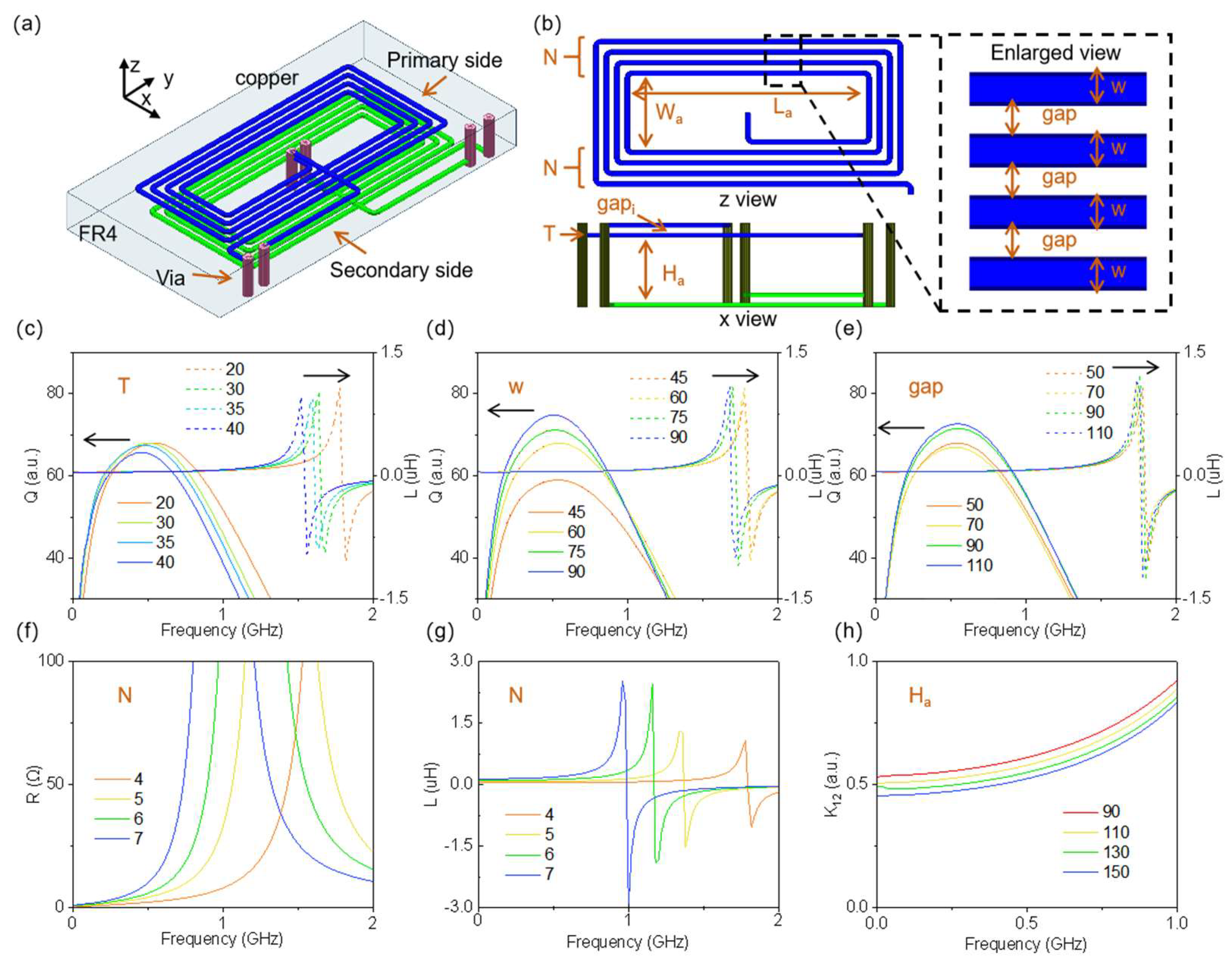
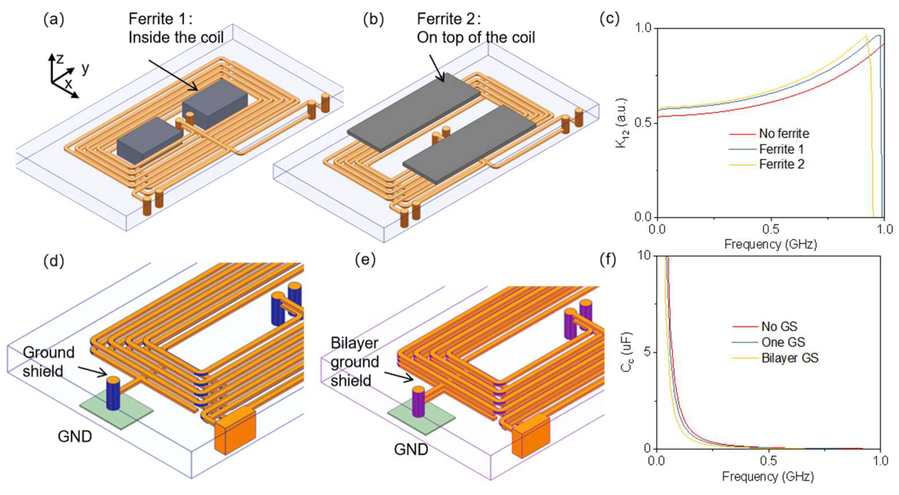
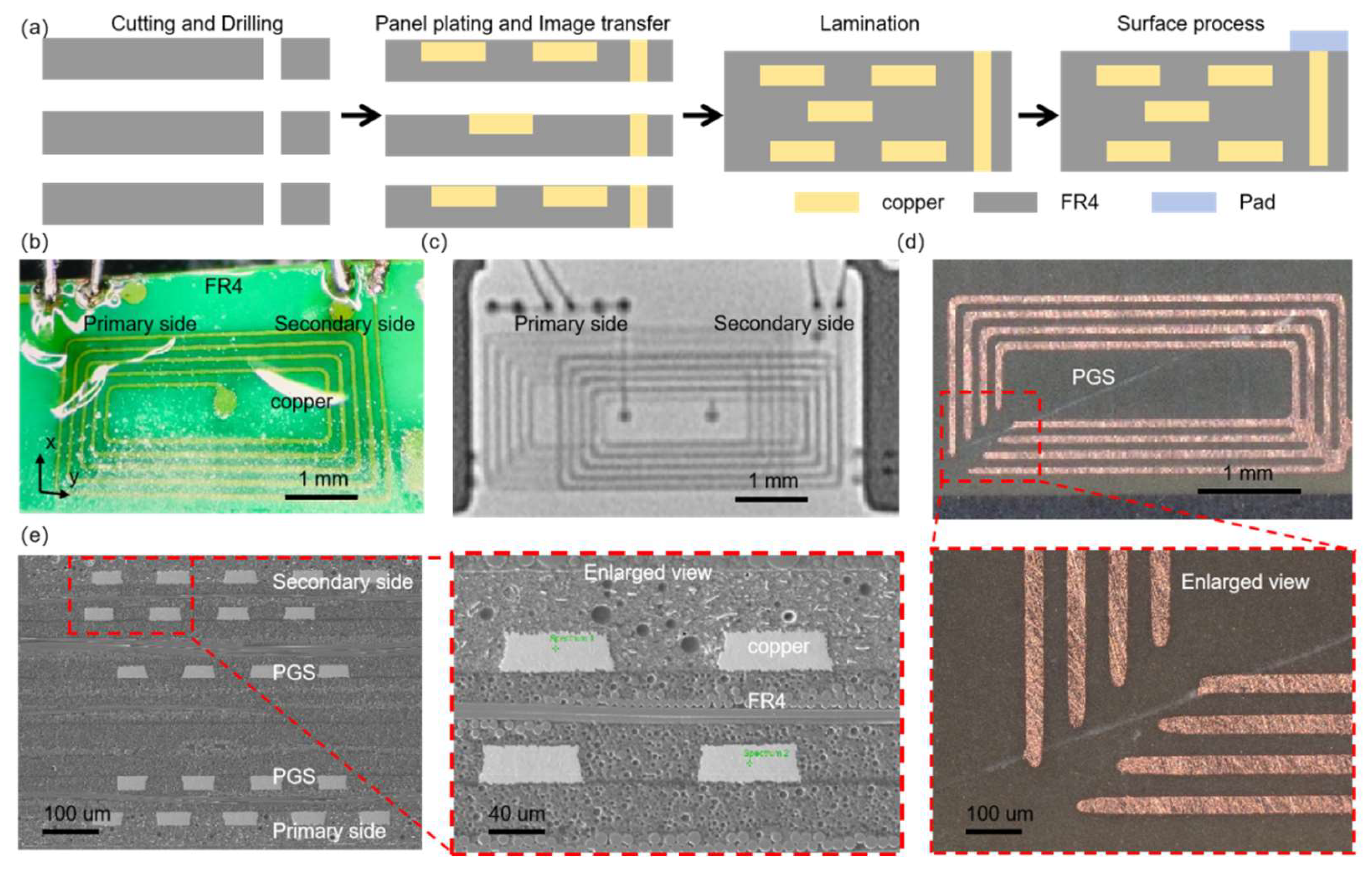
2. Design and Fabrication

Figure 1a shows the basic structure of the on-chip transformer. The primary and secondary coils are separated by FR4 material, with copper used as the coil material. Each coil consists of two layers, interconnected through copper plating in the Vias, allowing the formation of a three-dimensional structure of the transformer through stacked planar processing. Typical coil shapes include circular, elliptical, and rectangular [22]. Although complex winding or stacking structures can enhance the inductance [23], they increase the number of variables in the design and manufacturing processes, resulting in a significant increase in simulation workload. Therefore, this paper only selects equidistant rectangular coil patterns, as shown in Figure 1b.
The self-inductance, coupling efficiency, and equivalent resistance of the on-chip transformer are frequency-dependent. Due to lower coupling efficiency at low frequencies, these transformers generally operate above 10 MHz. The quality factor Q indicates the energy loss of the coil in alternating signals. The gain coefficient is an important parameter for the on-chip transformer, calculated as follows [24-26]:
A v = V 2 V 1 k 12 L 2 L 1 j ω L 1 j ω L 1 + R 2 + R L O A D
Where V 2 is the peak-to-peak voltage of the secondary coil, V 1 is the peak-to-peak voltage of the primary coil, k 12 is the coupling efficiency between the two coils, L 1 and L 2 are the self-inductance values of the primary and secondary coils respectively, R 2 and R L O A D are the equivalent resistances of the secondary coil and load respectively, and ω is the angular frequency.
We obtained the frequency characteristics of the on-chip transformer using a finite element simulation method, as shown in Figure 1c-h. We optimized multiple parameters, including copper layer thickness T, copper wire width w, copper wire spacing gap, number of turns N, and spacing Ha between the primary and secondary sides. The results indicate that increasing T and N lowers the cutoff frequency and improves the self-inductance value at specific frequencies; increasing w effectively enhances the Q value; while increasing N reduces the equivalent resistance and minimizes inductive losses. Decreasing Ha can effectively improve coupling efficiency, whereas increasing Ha helps to enhance isolation levels. Considering the transformer’s size, available process adjustment space, and performance optimization, we ultimately selected a set of structural parameters to meet the needs of the isolation driver circuit. Specific parameters are withheld due to commercial confidentiality.
Improving the coupling efficiency of the on-chip transformer is crucial, as higher efficiency means lower losses [27]. Using magnetic cores with higher permeability can enhance coupling efficiency [28,29]. Figure 2a shows the structure with a magnetic core directly embedded in the center of the coil, while Figure 2b shows the structure with a magnetic material pattern added on the surface of the on-chip transformer. Figure 2c displays the finite element simulation results. While the presence of the magnetic core effectively improves coupling efficiency, the improvement is typically limited to about 15% due to the volume constraints of the magnetic core. Additionally, the ferrite 1 option presents significant challenges in planar process, whereas ferrite 2 is compatible with planar process but offers negligible improvement in coupling efficiency, making it hard to justify the additional manufacturing costs brought by the process enhancements. Hence, this paper does not adopt a magnetic core structure.
To enhance the Common Mode Transient Immunity (CMTI) of the on-chip transformer, we placed a patterned metal layer above the secondary coil, forming a grounded metal structure that creates a Faraday shield. By employing a ground shield (GS) pattern that does not form a closed loop, the eddy currents induced by the magnetic field in the GS are suppressed, thus not affecting the normal functioning of the OCT. Meanwhile, the electric field from the primary coil is primarily intercepted by the GS. Therefore, during common mode voltage transients, the displacement current caused by capacitive coupling is directed to ground through the secondary's PGS, reducing interference in the output signal [21].
In traditional OCTs, the output voltage caused by common mode transients (dVCM/dt) couples to the secondary output through an equivalent capacitance CC, which is proportional to the CC value [30-33]. We employed finite element analysis to establish the three-dimensional models shown in Figure 2d,e, with the frequency characteristics of CC presented in Figure 2f. The presence of the GS effectively reduces the equivalent capacitance CC; for instance, at a frequency of 0.1 GHz, the CC value of the double-layer GS is only half that of the case without GS layer. Considering the trade-off between manufacturing costs and device performance, this paper chooses to implement a double-layer GS structure
Figure 3a outlines the processing flow for the on-chip transformer, which is compatible with mature PCB manufacturing techniques. The process begins with cutting raw materials and drilling holes at designated via locations. Next, each layer undergoes copper plating and patterning. Given that the manufacturing precision is at the micrometer level, the cost of the patterning process is relatively low. Subsequently, multilayer materials are aligned, stacked, and bonded. Finally, interconnection ports are created on the surface for external electrical connectivity. Figure 3b shows a photograph of the processed on-chip transformer, indicating that the procedure is simple and reliable, making it suitable for mass production.
To assess the reliability of the on-chip transformer fabricated using this PCB process, a series of characterization experiments were conducted. Figure 3c presents an X-ray tomography image of the on-chip transformer, revealing no delamination, voids, bubbles, or impurities that could negatively affect performance. Figure 3d shows the pattern of the ground shielding layer after layer removal and grinding, with uniform copper wire widths, maintaining a width consistency within 3% and a spacing consistency within 2.6%. Simulations were conducted to supplement the analysis of manufacturing tolerances, which were found to be within acceptable limits. Figure 3e displays cross-sectional scanning electron microscope (SEM) images of the device, indicating that the consistency of copper layer thickness is within 5%. However, due to the limitations of the pressing process, interlayer spacing has a relatively larger manufacturing tolerance, with a maximum deviation of up to 12%. These errors must be considered in circuit design adjustments, as evaluated through simulation. The insulation level of FR4 material ranges from 16 to 20 V/μm, implying that a 200 μm thick FR4 layer can withstand at least 3 kV of electrical arcing. These results demonstrate the advantages of the PCB technology-based on-chip transformer in terms of fabrication and reliability, laying a solid foundation for subsequent applications

3. Results and Discussion

We use a behavioral-level circuit model for the on-chip transformer [25], as shown in Figure 4a. This model serves as a standard unit during the chip design process, with parameters such as R, M, L, K, and Q defined based on simulation results to establish their operational ranges. Through behavioral-level simulations, we determined the range of voltage gain A v , optimizing the goal to ensure that the fluctuations of A v do not exceed 20%. Figure 4b displays the input and output waveforms of the primary and secondary sides at a frequency of 90 MHz, where the value of A v is measured at 1.21.
To validate our simulations experimentally, we constructed the testing platform illustrated in Figure 4c, along with a photograph of the oscilloscope used during the testing. A signal generator supplies a sine wave at a specified frequency to the primary side, while the oscilloscope measures the secondary side signal. As shown in Figure 4d, at a frequency of 90 MHz, the input and output waveforms of the primary and secondary sides yield an A v value of 1.25. After extensive iterative experiments and optimization of simulation parameters, we successfully achieved a deviation in A v between simulated and actual measurement results of no more than 5%. This outcome provides a stable technological platform for realizing high-consistency isolation driver products and demonstrates the reliability and effectiveness of the designed on-chip transformer in practical applications.
Figure 5a presents a simplified circuit block diagram of the isolated driver circuit. When the input signal is fed into the circuit, the CTR module applies enable control signals to other modules based on the input signal, which is shown in Figure 5e. After introducing a 90 MHz oscillation, the signal is passed through the driver circuit to the on-chip transformer, then processed through waveform shaping and wide-threshold Schmidt trigger circuits (SMT). The output signal experiences a slight delay, enabling the signal to transition from a low voltage region in the front stage to a high voltage region in the subsequent stage.
The isolated driver chip comprises three main parts: die1 (input section), the on-chip transformer, and die2 (output section), which are integrated on a bus via SIP, as depicted in Figure 5b. Figure 5c,d illustrate two circuits directly connected to the on-chip transformer. When the input signal is set at 5V, the generator (OSC) is activated, outputting an oscillating signal ranging from 0 to 5V. The output from the Driver circuit generates a driving signal between -5V and 5V, as shown in Figure 5f. The use of non-overlapping clocks prevents signal interference, creating a zero-volt level between -5V and 5V, exemplified by the waveform characteristics in the red dashed box.
After passing through the transformer, the signal becomes an AC voltage range of -5.5V to 5.5V, with a supply voltage (VDD) of 10V in the subsequent stage. The waveform shaping circuit processes the signal, moving it to a higher voltage threshold and achieving a single-ended output, as illustrated in Figure 5g. Through optimized design, the low conversion threshold of the Schmidt trigger circuit is set to 3V, allowing the oscillating signal component to rise to 10V via the level shifting module, while the non-oscillating signal portion remains at 0V, as shown in Figure 5h. This process enables efficient isolated signal transmission based on the on-chip transformer.

4. Conclusions

In summary, we have reported an on-chip transformer compatible with PCB processes, aimed at enabling isolated driver chips. This approach not only aligns with mature CMOS processes and PCB manufacturing methods but also offers low costs and significant commercial potential, while optimizing performance. Through finite element analysis, we designed the structure and utilized processes compatible with PCB techniques to fabricate the on-chip transformer. By combining X-ray imaging, layer removal photography, as well as simulation and testing analysis, we evaluated the consistency of the device production. Ultimately, guided by a fabless model, we successfully achieved wafer production and functioned the isolated driver chip. This on-chip transformer-based isolated driver chip demonstrates vast application prospects in various fields, including gate driving, new energy vehicles, and photovoltaic energy storage. Our research provides a solid foundation for the further development and application of these technologies, with the potential to drive technological advancements and innovations in related fields.

Author Contributions

The design and simulation of the experimental device in this paper were completed by Ye Luo, while manuscript proofreading and other tasks were collectively handled by all authors.

Funding

This work was supported by National Key Research and Development Program of China (×××××××××).

Institutional Review Board Statement

Not applicable.

Informed Consent Statement

Not applicable.

Data Availability Statement

The data presented in this study are available upon request.

Acknowledgments

The authors thank Ningbo CRRC Times Transducer Technology Co LTD and the College of Electrical Engineering at Zhejiang University for facility support.

Conflicts of Interest

The authors declare no conflicts of interest.

References

  1. Geng, C.; Luo, C.; Zhang, Z.; Wang, X.; Liu, Y.; Sun, B. Design and optimization of on chip thick plated copper transformers for galvanic isolated DC DC converter achieving up to 38.9% peak efficiency. Integr. 2023, 90, 146–156. [Google Scholar] [CrossRef]
  2. Derkaoui, M.; Benhadda, Y.; Chaabene, G.; Spiteri, P. On chip GaN planar transformer design for highly integrated RF systems. J. Circuits, Syst. Comput. 2023, 32. [Google Scholar] [CrossRef]
  3. Elalfy, D.A.; Gouda, E.; Kotb, M.F.; Bures, V.; Sedhom, B.E. Comprehensive review of energy storage systems technologies, objectives, challenges, and future trends. Energy Strategy Rev. 2024, 54. [Google Scholar] [CrossRef]
  4. SotoMarchena, D.; Barrero, F.; Colodro, F.; Arahal, M.R.; Mora, J.L. On site calibration of an electric drive: a case study using a multiphase system. Sens. 2023, 23. [Google Scholar] [CrossRef]
  5. Guo, Z.; Chu, L.; Hou, Z.; Wang, Y.; Hu, J.; Sun, W. A dual distribution control method for multi power components energy output of 4WD electric vehicles. Sens. 2022, 22. [Google Scholar] [CrossRef] [PubMed]
  6. Chen, C.; Pan, P.; Gu, J.; Li, X. A high voltage isolated MEMS quadsolenoid transformer with specific insulation barriers for miniaturized galvanically isolated power applications. Micromachines 2024, 15. [Google Scholar] [CrossRef]
  7. Mirfakhraei, S.S.; Audet, Y.; Hassan, A.; Sawan, M. A small footprint digital isolator based on CMOS integrated hall effect sensor. IEEE Sens. J. 2022, 22, 412–418. [Google Scholar] [CrossRef]
  8. Lv, G.; Ding, Y.; Fang, X.; Li, L.; Bai, F.; Sin, J.K.O.; Wu, R. A novel conformal thick oxide technology for on chip high voltage isolation. IEEE Trans. Compon. Packag. Manuf. Technol. 2022, 12, 704–706. [Google Scholar] [CrossRef]
  9. Mirfakhraei, S.S.; Audet, Y.; Hassan, A.; Sawan, M. A galvanic isolated amplifier based on CMOS integrated hall effect sensors. IEEE Trans. Circuits Syst. I Regul. Pap. 2021, 68, 1388–1397. [Google Scholar] [CrossRef]
  10. Derkaoui, M.; Benhadda, Y.; Hamid, A.; Temmar, A. Design and modeling of octagonal planar inductor and transformer in monolithic technology for RF systems. J. Electr. Eng. Technol. 2021, 16, 1481–1493. [Google Scholar] [CrossRef]
  11. Altoobaji, I.; Ali, M.; Hassan, A.; Nabavi, M.; Audet, Y.; Lakhssassi, A.; Ieee. A fully integrated on chip inductive digital isolator: design investigation and simulation. In Proceedings of IEEE MWSCAS, 2020; pp. 868-871.
  12. Massaro, A. Artificial intelligence signal control in electronic optocoupler circuits addressed on industry 5.0 digital twin. Electron. 2024, 13. [Google Scholar] [CrossRef]
  13. Dwivedi, A.K.; Agarwal, L.; Bajpai, T.; Tripathi, S. Er doped ZnO/SnS2 PEDOT:PSS double heterostructure photodetector and Its application as optocoupler. IEEE Sens. J. 2024, 24, 25609–25616. [Google Scholar] [CrossRef]
  14. Pan, D.; Xiong, Z.; Lu, Q.; Miao, F.; Wu, L.; Cheng, L. A 250 Mb/s on chip capacitive digital isolator with adaptive frequency control. IEEE Solid-State Circuits Lett. 2024, 7, 231–234. [Google Scholar] [CrossRef]
  15. Altoobaji, I.; Hassan, A.; Ali, M.; Audet, Y.; Lakhssassi, A. A low power 0.68 Gbps data communication system for capacitive digital isolator with 1.9 ns propagation delay. IEEE Trans. Very Large Scale Integr. VLSI Syst. 2024, 32, 952–956. [Google Scholar] [CrossRef]
  16. Wu, R.X.; Chen, J.L.; Liao, N.T.; Fang, X.M.; Ieee. On chip transformers with shielding structures for high dV/dt immunity isolated gate drive. In Proceedings of IEEE ECCE.
  17. Wang, N.N.; Miftakhutdinov, R.; Kulkarni, S.; O'Mathuna, C. High efficiency on Si integrated microtransformers for isolated power conversion applications. IEEE Trans. Power Electron. 2015, 30, 5746–5754. [Google Scholar] [CrossRef]
  18. Peng, L.; Wu, R.; Fang, X.; Toyoda, Y.; Akahane, M.; Yamaji, M.; Sumida, H.; Sin, J.K.O.; Ieee. A novel 3D TSV transformer technology for digital isolator gate driver applications. In Proceedings of ISPSD, 2013; pp. 69-72.
  19. Bajwa, R.; Yapici, M.K. Integrated on chip transformers: recent progress in the design, layout, modeling and fabrication. Sens. 2019, 19. [Google Scholar] [CrossRef] [PubMed]
  20. Macrelli, E. Roll up for three dimensional transformers. Nat. Electron. 2018, 1, 270–271. [Google Scholar] [CrossRef]
  21. Wu, R.X.; Chen, J.L.; Fang, X.M. A novel on chip transformer with patterned ground shield for high common mode transient immunity isolated signal transfer. IEEE Electron Device Lett. 2018, 39, 1712–1715. [Google Scholar] [CrossRef]
  22. Tiemeijer, L.F.; Pijper, R.M.T.; Andrei, C.; Grenados, E. Analysis, design, modeling, and characterization of low loss scalable on chip transformers. IEEE Trans. Microwave Theory Tech. 2013, 61, 2545–2557. [Google Scholar] [CrossRef]
  23. Huang, W.; Zhou, J.; Froeter, P.J.; Walsh, K.; Liu, S.; Kraman, M.D.; Li, M.; Michaels, J.A.; Sievers, D.J.; Gong, S.; et al. Three dimensional radio frequency transformers based on a self rolled up membrane platform. Nat. Electron. 2018, 1, 305–313. [Google Scholar] [CrossRef]
  24. Zhu, K.; Chen, H.; Li, S.; Sun, C.; Liu, F. An RF on chip transformer with Fe3O4 GO nanocomposite film. IEEE Trans. Magn. 2021, 57. [Google Scholar] [CrossRef]
  25. Kaeriyama, S.; Uchida, S.; Furumiya, M.; Okada, M.; Maeda, T.; Mizuno, M. A 2.5 kV isolation 35 kV/us CMR 250 Mbps digital isolator in standard CMOS with a small transformer driving technique. IEEE J. Solid-State Circuits 2012, 47, 435–443. [Google Scholar] [CrossRef]
  26. Derkaoui, M.; Larbi, A.; Benhadda, Y. Comparative study of different topologies of monolithic on chip planar transformer for optical VCSEL driver. Electr. Power Compon. Syst. 2024, 52, 959–970. [Google Scholar] [CrossRef]
  27. Wang, N.; Chen, C.; Chen, P.; Gu, J.; Pan, P.; Han, R.; Liu, M.; Li, X. MEMS casting fabricated chip style 3D metal solenoidal transformers towards integrated power supply. Micromachines 2022, 13. [Google Scholar] [CrossRef] [PubMed]
  28. Chen, C.; Pan, P.; Lyu, D.; Gu, J.; Liu, M.; Li, X. Wafer level fabricated tight coupling dual solenoid transformer chips with watt scale power transfer. IEEE Trans. Power Electron. 2023, 38, 5118–5127. [Google Scholar] [CrossRef]
  29. Wu, H.; Lekas, M.; Davies, R.; Shepard, K.L.; Sturcken, N. Integrated transformers with magnetic thin films. IEEE Trans. Magn. 2016, 52. [Google Scholar] [CrossRef]
  30. Bansal, U.; Garg, A.; Shalini, D. A review on recently reported grounded CMOS active inductors. Wireless Pers. Commun. 2023, 133, 913–949. [Google Scholar] [CrossRef]
  31. Hamid, S.S.; Mariappan, S.; Rajendran, J.; Rawat, A.S.; Rhaffor, N.A.; Kumar, N.; Nathan, A.; Yarman, B.S. A state of the art review on CMOS radio frequency power amplifiers for wireless communication systems. Micromachines 2023, 14. [Google Scholar] [CrossRef]
  32. Li, X.; Ni, Z.; Gu, L.; Wu, Z.; Yang, C. Micromachined high performance RF passives in CMOS substrate. J. Micromech. Microeng. 2016, 26. [Google Scholar] [CrossRef]
  33. Yang, R.; Hou, H.; Wang, Y.; Fu, L. Micro magnetofluidics in microfluidic systems: a review. Sens. Actuators, B 2016, 224, 1–15. [Google Scholar] [CrossRef]
Figure 1. Structure and Simulation of On-Chip Transformer. (a) Three-dimensional view of the on-chip transformer; (b) Z-direction and X-direction views of the coil; (c) Effect of changing the copper layer thickness T of the coil on the relationship between Q value, L value, and frequency; (d) Effect of changing the coil copper wire width w on the relationship between Q value, L value, and frequency; (e) Effect of changing the coil copper wire spacing gap on the relationship between Q value, L value, and frequency; (f) Effect of changing the number of turns N of the coil on the relationship between R value and frequency; (g) Effect of changing the number of turns N on the relationship between L value and frequency; (h) Effect of changing the spacing Ha between the primary side and secondary side on the relationship between K12 value and frequency.
Preprints 145552 g001
Figure 2. Influence of Magnetic Core and Ground Shielding Layer on On-Chip Transformer. (a) Three-dimensional structure with a magnetic core block added in the center of the coil; (b) Three-dimensional structure with a magnetic chip added above the coil; (c) Relationship between the presence of magnetic core and K12 value with frequency; (d) Three-dimensional structure of a single ground shielding layer; (e) Three-dimensional structure of a double ground shielding layer; (f) Relationship between the presence of ground shielding layer and CC value with frequency.
Preprints 145552 g002
Figure 3. Fabrication and Characterization of On-Chip Transformer. (a) Fabrication process of the on-chip transformer based on PCB technology; (b) Photo of the on-chip transformer (without surface treatment); (c) X-ray tomography image of the on-chip transformer; (d) Microscopic image of the ground shielding layer and its magnified view; (e) Cross-sectional SEM images of the on-chip transformer and a magnified view.
Preprints 145552 g003
Figure 4. Simulation and Experimental Testing of On-Chip Transformer. (a) Simplified circuit model of the on-chip transformer; (b) Input and output simulation results of the primary and secondary sides of the on-chip transformer; (c) Schematic diagram of the experimental testing setup for the on-chip transformer; (d) Input and output experimental testing results of the primary and secondary sides of the on-chip transformer.
Preprints 145552 g004
Figure 5. Simulation Results of Isolated Driver Circuit. (a) Simplified circuit block diagram of the isolated driver circuit; (b) Photo of the isolated driver packaged in SIP (System in Package) format; (c) Output circuit structure of the Driver circuit; (d) Input circuit structure of the Waveform shaping circuit; (e) Signal at the VIN terminal; (f) Differential signal output at OUT1 port, with the waveform magnified on the horizontal axis within the red dashed box; (g) Single-ended signal output from the Waveform shaping circuit, with the waveform magnified on the horizontal axis within the red dashed box; (h) Single-ended signal output at the VOUT terminal.
Preprints 145552 g005
Disclaimer/Publisher’s Note: The statements, opinions and data contained in all publications are solely those of the individual author(s) and contributor(s) and not of MDPI and/or the editor(s). MDPI and/or the editor(s) disclaim responsibility for any injury to people or property resulting from any ideas, methods, instructions or products referred to in the content.
Copyright: This open access article is published under a Creative Commons CC BY 4.0 license, which permit the free download, distribution, and reuse, provided that the author and preprint are cited in any reuse.
Prerpints.org logo

Preprints.org is a free preprint server supported by MDPI in Basel, Switzerland.

Subscribe

Disclaimer

Terms of Use

Privacy Policy

Privacy Settings

© 2025 MDPI (Basel, Switzerland) unless otherwise stated