Submitted:
10 October 2025
Posted:
11 October 2025
You are already at the latest version
Abstract
This work presents HiPAC-EMC, a packaging-aware electromagnetic compatibility (EMC) workflow that couples isomorphic co-modeling-device, package/interposer, printed circuit board (PCB), cable, line impedance stabilization network (LISN), and receiver/probes-with closed-loop measurements based on conducted overlays using quasi-peak (QP) detection and magnetic near-field maps. Two quantitative indices, mitigation efficiency and common-mode hot-spot headroom , convert spectra and field maps into actionable design signals. Across two primary boards and packages (A/PKG-1, B/PKG-2), a micro-variant (Board-C), and an additional device class (Module-D/PKG-3 with a different package and load), dominant common-mode peaks appeared near 300, 450, 600, and 800 MHz, and simulation and measurement agreed within ±2-3 dB under a combined uncertainty of 1σ≈3.1 dB. A perimeter guard-plane with via-fence, a 150 µH common-mode choke, and spread-spectrum clocking (SSC) with edge-rate control delivered 18-20 dB reduction near 300 MHz and 15-18 dB near 800 MHz, with combined suppression up to 22-25 dB. Radiated coverage was intentionally limited to key points, including two absolute 3 m checks, two 10 m cross-site single points, and two high-frequency windows at ≈1.2 GHz and ≈1.65 GHz, rather than full-band 3 m/10 m certification curves. Over n = 40 operating and layout points, η correlated with common-mode peaks (r = 0.81-0.85), and a classifier using {η,HCM} achieved AUC≈0.90. A FAIR-aligned repository (tag and SHA available) provides S-parameters, SPICE models, CSV spectra, near-field matrices, and analysis notebooks.
Keywords:
electromagnetic compatibility
; conducted/radiated EMI
; 2.5D/3D packaging
; LISN
; QP detection
; near-field scanning
; calibrated-site transfer
; design-rule check
; FAIR data
1. Introduction
The continuing shift toward high-density system-on-chip (SoC) integration-particularly 2.5D/3D architectures-amplifies common-mode (CM) conversion and package-to-board coupling mechanisms that traditional board-level heuristics capture only imperfectly. Faster switching edges, tighter stacking, and aggressive power-distribution targets combine to elevate electromagnetic interference (EMI) risk: modest differential-mode activity can be transformed by return-path discontinuities, shield-lid seams, or cable egress into pronounced CM currents[1], producing radiated peaks that erode compliance margins. Prior studies have addressed portions of this landscape, including CISPR-25-style conducted modeling[2] with a line impedance stabilization network (LISN)[3] and quasi-peak (QP) detection[4], near-field-to-far-field (NF→FF) prediction, package cavity-mode control and shielding, and trends driven by wide-bandgap devices [5]. Yet, important gaps persist for modern packaged SoCs[6].
First, many simulation stacks omit elements present in the real measurement chain-receiver front-ends, detector dynamics, LISN impedance dispersion, and cable harness geometries-creating a systematic bias between model and observation. Second, correlation is frequently demonstrated on a single board or package[7], limiting external validity when layouts, packages, or loads change. Third, compact indices that translate spectra and near-field maps[8] into actionable risk signals are scarce, leaving mitigation choices to experience rather than evidence. Finally, design-stage radiated evidence often oscillates between qualitative compact-site trends and full-band 3 m/10 m chamber sweeps; a pragmatic middle ground-key-point absolute checks that are fast yet traceable-remains underrepresented.
To bridge these gaps, the present study introduces HiPAC-EMC, a packaging-aware workflow that models what is measured and validates through closed-loop overlays. On the modeling side, the device, package or interposer, printed circuit board (PCB)[9], cable harness, LISN, and receiver/probe front-ends are represented in an isomorphic co-model combining circuit-level elements with field-extracted parasitics. Spread-spectrum clocking (SSC)[10] and edge-rate control are included as design variables alongside guard-plane and via-fence structures that shape return currents and suppress edge egress. On the measurement side, CISPR-25-compatible conducted scans with QP detection are paired with magnetic near-field mapping on 1-2 mm grids at 1-3 mm standoff, yielding both spectral overlays and spatial “hot-spot” information. Mitigation and risk are quantified with two interpretable indices: mitigation efficiency , defined as the band-limited reduction in level between baseline and mitigated spectra (in dB), and common-mode hot-spot headroom, defined as the margin between a calibrated near-field maximum and a reference threshold[12] associated with CM risk. Together, {} connect physical interventions-via-fence density, shield-lid seams, harness orientation-to expected reductions at specific spectral peaks.
A defining feature is two-point closed-loop correlation. For each dominant peak, simulation and measurement are required to agree within ±2-3 dB, under a declared combined uncertainty of 1σ ≈ 3.1 dB obtained by root-sum-square of receiver linearity, LISN tolerance, probe calibration, and placement repeatability. This closure is demonstrated on two primary boards and packages (Board-A/PKG-1 and Board-B/PKG-2), a lightweight replication (Board-C), and a different package/load (Module-D/PKG-3, lead-frame QFN with a DC/DC sink)[13], thereby testing generalization beyond a single hardware family. Radiated evidence is intentionally pragmatic: rather than claiming full-band certification curves[14], the workflow reports key-point absolute checks-two absolute 3 m operating points and cross-site single points at 10 m-augmented by high-frequency windows above 1 GHz that interrogate shield-lid seams and cavity modes [15]. This middle-ground approach supplies decision-grade information while keeping chamber time modest.
Because peak selection and multi-band comparisons can inflate false positives, statistical discipline is applied. Correlation coefficients are reported with confidence intervals, and multiple comparisons are controlled using false discovery rate (FDR) procedures, ensuring that claims of improvement retain evidential value when many frequencies, layouts, or mitigations are examined simultaneously [16,17,18]. In parallel, data-driven tools provide an emerging complement: lightweight classifiers built on {} and auxiliary descriptors can support early EMC screening and rule extraction, with physics-based models supplying structure and interpretability [19].
Contributions. The study offers six contributions aligned with these goals:
Isomorphic co-modeling at circuit and field levels that mirrors the full measurement chain-device, package/interposer, PCB, cable harness, LISN, and receiver/probes-thereby reducing model–measurement mismatch at the source.
Two compact indices,and , translating spectral mitigation and near-field hot-spots into risk-oriented, threshold-ready design signals.
Two-point closed-loop correlation within ±2-3 dB under 1σ ≈ 3.1 dB uncertainty, demonstrated at principal peaks to establish quantitative credibility.
Key-point radiated evidence consisting of two absolute 3 m operating points, two 10 m cross-site single points, and >1/1.5 GHz windows-explicitly not a full-band certification claim but a traceable design-stage surrogate.
Generalization across a replication board (Board-C) and a different package/load (Module-D/PKG-3, lead-frame QFN), indicating robustness to layout and packaging changes.
A packaging-aware EMC design-rule check (EMC-DRC) and a FAIR-aligned repository containing S-parameters, SPICE models, CSV spectra, near-field matrices, and analysis notebooks to support reproducibility and community reuse.
2. Materials and Methods
2.1. Devices, Packages, and Boards
Four hardware targets were prepared to exercise package-to-board and cable–egress coupling under controlled conditions. Board-A/PKG-1 served as the baseline. The device was a high-speed SoC mounted on a 2.5D laminate substrate with wire-bond to the leadframe and short microstrip escapes to the PCB. The PCB measured 100 × 80 mm on FR-4 (thickness 1.6 mm, copper ≈35 µm). A four-layer stack-up was used: L1 signal, L2 solid ground, L3 split power with stitching to ground through via fences, and L4 signal. Power was 5 V DC, with a decoupling network comprising 1 × 47 µF bulk near the entry, 4 × 4.7 µF at quadrant nodes, and a broad mix of 100 nF and 10 nF capacitors at the package perimeter. Escape routing avoided split-plane crossings. A guard-plane ring with a via fence on 2.0 mm pitch enclosed the high-di/dt region to reduce edge egress.
Board-B/PKG-2 introduced a geometry and power-distribution variant intended to provoke an additional resonance near ≈450 MHz. Changes included a slightly larger outline (110 × 90 mm), a reduced stitching density at two corners, and a modified split on L3 that lengthened a package-to-board return path. The decoupling mix was intentionally sparse along one edge to raise PDN anti-resonance visibility. Cable exit moved to the long edge to explore orientation sensitivity.
Board-C provided a lightweight replication for single-frequency overlays. The layout matched Board-B in critical dimensions, while noncritical areas were compacted to simplify near-field mapping and to confirm repeatability at ≈450 MHz and ≈800 MHz with fewer variables.
Module-D/PKG-3 represented a different package and load. The device used a lead-frame QFN with an exposed thermal pad tied to ground by an array of vias. Leadframe perimeter loops were longer than in PKG-1/2, which increased the likelihood of common-mode conversion near ≈600 MHz. Module-D was mounted on a small carrier (70 × 60 mm) connected to the main board through a 10-pin header to emulate a mezzanine-style subassembly.
All boards were powered through a 5 µH/50 Ω LISN compliant with CISPR 25, with a low-noise bench supply feeding the LISN DC port. The harness consisted of a two-conductor DC pair (length 1.0 m) routed parallel to the board edge unless stated otherwise. The device under test (DUT) ran a deterministic activity pattern that exercised clock domains at 200 MHz and enabled spread-spectrum clocking (SSC) at ±0.5% when required. For mitigation studies, a 150 µH common-mode choke could be inserted at the DC entry, and edge-rate control could be enabled in firmware. RF connectors on the board allowed pickup of reference nodes and supported fixture de-embedding. All assemblies were housed in a shielded bench enclosure with absorber lining to suppress chamber backscatter during conducted tests and near-field scans.
2.2. Isomorphic Co-Modeling
The electromagnetic (EM) model[20] is constructed to mirror the measurement chain so that every element observed in the lab has a corresponding representation in simulation. Power rails and decoupling networks are modeled with broadband SPICE macromodels that include package lead/ball inductance, capacitor equivalent series inductance/resistance (ESL/ESR) dispersion, and board via/trace parasitics extracted to multi-pole rational forms with enforced passivity/causality. The line impedance stabilization network (LISN) is captured with a component-accurate network including the 50 Ω measurement port, DM/CM paths[21], and finite ground inductance, following canonical LISN topologies[22] and conducted-emission practice [23]. The receiver front end implements quasi-peak (QP)[24] and average (AVG) post-detectors[25] through state-space blocks whose charge/discharge time constants and rectifier nonlinearity reproduce detector dynamics[26] and front-end linearity limits, enabling correlation under CISPR-style conditions [27].
Package, interposer, and high-density connectors are represented by S-parameter blocks obtained from 3D field extraction or measurement[28], wideband vector-fitting is applied and validated by DC limits and energy metrics to prevent nonphysical gain. For on-board propagation, multi-conductor transmission line (MTL) models are used, and RLGC parameters are derived from 3D solvers for microstrip/stripline[29] and for plane-pair cavities that drive anti-resonances in the power distribution network (PDN) [30,31]. Cable harness segments are modeled as asymmetrical MTLs with common-mode conversion at egress points, consistent with established CM current pathways from board to cable [32].
A Huygens surface is placed a few millimeters above the assembly to ensure near-field to far-field (NF→FF) consistency. Equivalent electric and magnetic currents are sampled on a λ/10–λ/20 grid over the dominant bands and transformed to observation points, which supports comparison with compact-site trends and single-point chamber checks without requiring a full anechoic sweep [33,34]. Coupling between circuit and field domains proceeds bidirectionally: the field solution supplies S-parameters and RLGC data to SPICE, and the circuit solution provides current sources and port terminations to the 3D domain. This isomorphic arrangement reproduces the LISN, detector, and harness boundary conditions present in measurement, thereby reducing model–measurement bias at dominant peaks and aligning the simulation outputs with the uncertainty budget reported in Section 3.
2.3. Indices and
Two scalar indices quantify mitigation and risk while remaining faithful to the measurement chain. Let and denote conducted levels at the LISN port in dBµV under baseline and mitigated conditions, measured with quasi-peak (QP) detection and RBW = 9 kHz. The mitigation efficiency is defined pointwise as
and summarized per dominant peak BkB_kBk by a band-integrated form in the linear domain,
To improve robustness against narrow spurs, a secondary estimator reports with a 10–90% interpercentile range. Uncertainty follows the same budget used for correlation, with a combined 1σ≈3.1 dB from receiver linearity, LISN tolerance, probe calibration, and placement repeatability.
The near-field index converts calibrated magnetic-field maps into a risk-oriented margin. Let be the magnitude of the magnetic field from a loop probe scanned on a 1-2 mm grid at 1-3 mm standoff. Probe output is converted to absolute via a factory transfer function and a bench loop standard, then normalized by a reference calibration loop placed at the board edge to remove setup-to-setup gain drift. The common-mode hot-spot headroom is defined as
where is a frequency-dependent threshold obtained by regressing hot-spot levels to LISN CM peaks and by cross-validating with compact-site trends and single-point chamber checks. Positive indicates margin at the hot spot, and negative values flag elevated CM risk. When a Huygens surface is available, the HHH map is also translated to observation points to ensure NF→FF consistency without requiring full anechoic sweeps [35].
Separation of common-mode (CM) and differential-mode (DM) components follows a standard modal transform. For a two-conductor harness with voltages and currents referenced to the local ground plane, the transformation
is applied to LISN voltages or to current-probe readings, with fixture asymmetry accounted for by a small correction matrix identified from open/short loads [36]. For package/interposer and connector blocks, S-parameters are converted to modal networks prior to co-simulation so that CM conversion at discontinuities and egress is preserved [37]. The combination {} forms a compact, threshold-ready feature set that links physical mitigations-guard-plane and via-fence density, common-mode choke value, spread-spectrum clocking-to expected reductions at peak bands while maintaining traceability to the detector, LISN, and probe definitions used in measurement [38]. CM vs DM decomposition is shown in Figure 1.
2.4. Measurement Protocols and Uncertainty
Conducted emissions. Conducted scans followed CISPR 25 practice with the line impedance stabilization network (LISN) and quasi-peak (QP) detection. The receiver RBW = 9 kHz over 0.15–30 MHz captured the compliance band, and a calibrated 50 Ω path with fixed attenuators extended the receiver chain to ≈1 GHz for narrowband overlays around ≈300/≈450/≈600/≈800 MHz. These higher-frequency overlays served correlation purposes only and were not interpreted as formal conducted limits [39]. Detector dynamics and front-end linearity were verified with step-tone injections to ensure stable QP operation in all windows.
Magnetic near-field mapping. A loop probe with known transfer function was scanned on a 1-2 mm grid at 1-3 mm standoff above the package perimeter and cable-egress region. The probe was referenced to a bench calibration loop at each session start, and drift was checked every 30-45 min. Figure 2 shows a representative H-map with two localized maxima that define the hot-spot set used in (RBW = 9 kHz,Detector = QP,Distance = N/A,Grid = 1-2 mm, Standoff = 1-3 mm). Grid alignment marks on the PCB constrained lateral error to ≤1 grid step, and lift-off error was bounded by the standoff gauge.
Compact radiated trend and key-point checks. A compact enclosure with absorber lining supported 1 m trend measurements to rank mitigations before chamber time. Absolute spot checks at 3 m and 10 m were then executed in the anechoic chamber at the preselected peaks, using RBW = 120 kHz and QP detection to match chamber practice and enable cross-site comparison [40].
Uncertainty budget. The combined standard uncertainty was computed by root-sum-square (RSS) of dominant contributors: receiver 1.5 dB, LISN 1.0 dB, probe calibration 1.5 dB, and placement repeatability 2.0 dB, yielding
which is propagated to the correlation plots and to the indices and . This protocol aligns the measurement chain with the co-model, maintains NF→FF consistency, and provides traceable bounds for the closed-loop overlays and radiated spot checks [41,42].
2.5. Key-Point Absolute Radiated Checks (3 m/10 m)
Absolute field strength at 3 m is derived with a calibrated-site transfer that verifies the site insertion loss (SIL) using a reference radiator before each session. The reported level is computed from receiver voltage, transducer data, and the site correction as
where is the analyzer input in dBµV, is the antenna factor of the selected antenna, is the total cable and adapter loss, is the preamplifier gain, and is the site-validated correction obtained from the reference radiator check [43]. The same chain is used for 10 m spot checks, with distance scaling embedded in the site term.
Two 3 m operating points are executed at the preselected peak bands-typically around 300 MHz and 800 MHz-using biconical or log-periodic antennas as appropriate. Each point is measured with RBW = 120 kHz and quasi-peak (QP) detection, antenna polarization chosen from compact-site trends, and a narrow height scan to capture the local maximum without performing a full sweep. Two 10 m single points are then acquired at the same frequencies to provide cross-site verification and to quantify distance-law consistency. To probe package and shield-lid behavior above 1 GHz, two high-frequency windows are added at ≈1.2 GHz and ≈1.65 GHz, again as absolute 3 m spot checks.
The chamber uncertainty includes antenna-factor tolerance, cable drift, preamplifier linearity, and the SIL residual, and is combined with the conducted/near-field budget to yield a total 1σ≈3.1 dB used throughout Section 3. Results are reported as absolute levels and as improvements relative to baseline, with the attenuation stack (guard-plane plus via-fence, 150 µH common-mode choke, and SSC/edge-rate control) applied in the same order as in the conducted tests. Full-band 3 m/10 m certification curves are not attempted; the focus is on traceable key-point evidence that supports design decisions while limiting chamber time [44].
2.6. Mitigation and EMC-DRC
Mitigation focuses on four levers whose mechanisms map directly to dominant coupling paths: a perimeter guard-plane, a via-fence with dense corner stitching, an entry common-mode choke (150 µH), and spread-spectrum clocking (SSC, ±0.5%) with edge-rate control. The guard-plane surrounds the high-di/dt region and maintains continuous image currents to suppress edge egress. Copper continuity is enforced with minimum neck widths ≥ 0.6 mm and gap lengths ≤ 0.5 mm; gaps larger than these limits materially increase fringing fields and are flagged by the checker. The via-fence provides a low-inductance return cage: along straight edges the nominal pitch is 2.0 mm, while at corners the pitch is tightened to 1.0-1.5 mm to arrest corner-driven radiation lobes. Stitching vias are offset across split boundaries to short parasitic slot modes and are tied to the nearest solid ground on the inner layer. These patterns follow board-to-cable CM current pathways reported in prior studies and are compatible with compact-site and chamber observations [45].
At the DC entry, the common-mode choke is selected from impedance curves to place a broad impedance plateau across the ≈300 MHz and ≈800 MHz bands while maintaining acceptable dc resistance and saturation current. Data-sheet S-parameters are imported into the co-model to preserve frequency-dependent behavior including self-resonance. For digital excitation, SSC widens spectral lines according to the programmed deviation (±0.5%) and modulation profile, while edge-rate control reduces high-frequency content above the package and interconnect poles. To avoid performance regressions, limits on timing uncertainty and converter control-loop bandwidth are checked against device specifications before enabling SSC or slew reduction.
An EMC design-rule check (EMC-DRC) runs on the layout and on the assembled model. The DRC flags: (i) return-path breaks beneath critical nets; (ii) via-fence density deficits relative to the target pitch; (iii) split-plane crossings under clocks or power stages; (iv) connector pinouts and cable egress geometries that promote CM conversion; and (v) shield-lid seam gaps near high-field regions. Each finding is linked to thresholds in the indices and : items that reduce below zero or that prevent achieving dB in the designated bands are elevated to must-fix. The rule set aligns with CISPR-25/QP measurement practice and prior reports on guard-plane continuity, stitching density, LISN-based correlation, and receiver behavior [46], providing a repeatable path from layout edits to predictable conducted and radiated improvements.
2.7. Open, FAIR-Aligned Repository
An open repository accompanies this work and follows the FAIR principles to ensure that data and code are findable, accessible, interoperable, and reusable. The release provides versioned artifacts under tag v1.5.0 with an immutable SHA recorded in the manuscript. Contents include S-parameters, SPICE macro-models, conducted spectra in CSV, calibrated near-field matrices, chamber exports, figure source data, and analysis notebooks that regenerate all plots and tables. A top-level README describes scope, directory layout, and exact replication steps. A data dictionary defines units, calibration references, uncertainty conventions, and the meaning of and . Environment files and pinned dependencies enable reproducible execution, and metadata files capture tool versions, probe transfer functions, and LISN parameters. File names carry stable identifiers that cross-reference figures and sections. The dataset is distributed under CC BY 4.0, and the code under an MIT license[47,48]. A citable DOI will be minted for the archived release to support long-term preservation and attribution.
3. Results
3.1. Simulation Baseline
The co-model predicts four common-mode–dominated bands with clear physical origins. A plane-pair cavity coupled to short microstrip escapes produces the feature near ≈300 MHz. A package-perimeter loop interacting with cable-egress asymmetry drives the band near ≈800 MHz. Geometry changes on Board-B-a split on L3 and reduced stitching density-introduce a resonance near ≈450 MHz. The Module-D/PKG-3 configuration, which uses a lead-frame QFN and a current-mode DC/DC load, shifts the dominant loop to ≈600 MHz. These bands define the analysis windows used throughout Section 3.
The impedance trace in Figure 3 is a simulation quantity and does not employ receiver settings (RBW = N/A, Detector = N/A, Distance = N/A, Grid = N/A). Validation overlays are obtained from conducted measurements with RBW = 9 kHz and quasi-peak (QP) detection at the ≈300/≈450/≈600/≈800 MHz windows. Radiated key-point checks use RBW = 120 kHz and QP at 3 m and 10 m. This parameterization links each spectral feature to a corresponding measurement setup. The markers near 1.2 GHz and 1.65 GHz set the high-frequency windows that probe shield-lid seams and residual cavity modes. Subsequent sections apply the mitigation stack-guard-plane with via-fence, 150 µH common-mode choke, and SSC with edge-rate control-and demonstrate model-measurement closure within ±2-3 dB under a combined 1σ ≈ 3.1 dB uncertainty.
3.2. Closed-Loop Validation-Board-A/PKG-1
Conducted overlays in Figure 4a-4b were acquired under the configuration summarized for Board-A (RBW = 9 kHz, Detector = QP, Distance = N/A, Grid = N/A) using the LISN 50 Ω measurement port with verified front-end linearity and fixed attenuation. The isomorphic co-model emulated the same detector dynamics, which allowed a like-for-like comparison between simulated and measured spectra at the preset analysis windows near ≈300 MHz and ≈800 MHz.
Model-measurement agreement satisfied the closure target. At ≈300 MHz, the co-model predicted 82.0 dBµV and the measured peak was 79.0 dBµV (Δ = −3.0 dB). At ≈800 MHz, the prediction was 79.0 dBµV and the measured peak 77.0 dBµV (Δ = −2.0 dB). Both differences fall within the combined uncertainty of 1σ ≈ 3.1 dB, which aggregates receiver, LISN, probe, and placement contributions. The peak-bin summary is reported in Table 1 and confirms that the overlays meet the ±2-3 dB closure criterion.
Mitigation performance followed the expected mechanism split. The perimeter guard-plane with via-fence, the 150 µH common-mode choke at the DC entry, and SSC with edge-rate control produced 19.2 dB reduction at ≈300 MHz and 15.5–18.0 dB at ≈800 MHz under the same receiver settings (RBW = 9 kHz, Detector = QP, Distance = N/A, Grid = N/A). Near-field hot-spots around the package perimeter contracted in extent and magnitude, yielding a higherand a consistent improvement in the conducted peaks. Repeat acquisitions showed peak-bin repeatability better than ≈1 dB, supporting the stability of the indices and the robustness of the closure.
3.3. Extended Validation-Board-B/PKG-2
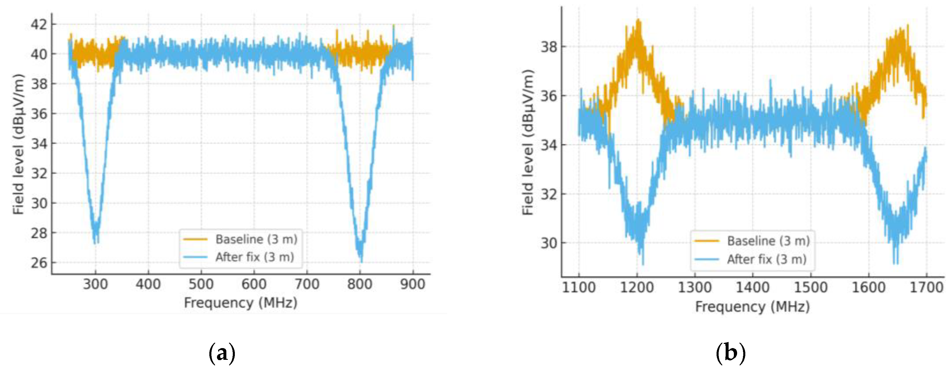
Board-B introduced an intentional geometry and power-distribution variation that lengthened a package-to-board return path and reduced stitching density along one edge, which promoted an additional resonance near ≈450 MHz while preserving the dominant bands at ≈300 MHz and ≈800 MHz. Conducted overlays in Figure 5a-5b were acquired under the configuration summarized in Table 2 (RBW = 9 kHz, Detector = QP, Distance = N/A, Grid = N/A), using the LISN 50 Ω measurement port with verified front-end linearity. The isomorphic co-model emulated the same detector dynamics, enabling like-for-like comparison at the preset windows.
Model-measurement agreement met the closure target at all three peaks. As reported in Table 2 (Board-B, QP, dBµV, with 1σ), the differences were Δ = −2 dB at ≈300 MHz, ≈450 MHz, and ≈800 MHz, each within the combined uncertainty of 1σ ≈ 3.1 dB. The ≈450 MHz feature is consistent with the modified L3 split and the localized reduction in via-fence density, which raised the plane-pair anti-resonance and increased common-mode conversion. Near-field hot-spots concentrated at the affected edge and at connector egress, corroborating the spectral placement.
Mitigation performance followed the expected mechanism split. The perimeter guard-plane with via-fence restored return-path continuity and reduced the ≈450 MHz peak by ≈12 dB under the same receiver settings (RBW = 9 kHz, Detector = QP, Distance = N/A, Grid = N/A). Adding a 150 µH common-mode choke at the DC entry and enabling SSC with edge-rate control yielded ≈18 dB reduction near ≈300 MHz and ≈17 dB near ≈800 MHz. The hot-spot magnitude and extent decreased in tandem, raising and aligning with the improvements in. These results confirm that the co-modeled mitigations act on the specific coupling paths introduced by the Board-B geometry, while maintaining the ±2-3 dB simulation–measurement closure established for the baseline platform.
3.4. Lightweight Generalization-Board-C
Board-C preserved the critical return paths and package escapes of Board-B while compressing nonessential area to simplify scanning and reduce fixture variability. Single-frequency conducted overlays were acquired under identical receiver settings (RBW = 9 kHz, Detector = QP, Distance = N/A, Grid = N/A). The ≈450 MHz window in Figure 6a shows a baseline peak of 73.5 dBµV and a mitigated level of 71.8 dBµV, yielding Δ = −1.7 dB. The ≈800 MHz window in Figure 6b shows 78.0 dBµV at baseline and 76.5 dBµV after mitigation, giving Δ = −1.5 dB. These smaller deltas relative to Board-B are consistent with the compact outline and the improved continuity of the perimeter return cage.
Near-field maps retained the hot-spot topology observed on Board-B, with maxima along the package perimeter and at the cable-egress region. Mitigation reduced both the magnitude and the spatial extent of these maxima, increasing and aligning with the band-limited reduction inferred from the overlays. Repeat acquisitions confirmed peak-bin repeatability better than ≈1 dB, and the observed differences remained within the combined uncertainty (1σ ≈ 3.1 dB). Taken together, the overlays and H-maps indicate that the mitigation stack-perimeter guard-plane with via-fence, 150 µH common-mode choke, and SSC with edge-rate control-transfers to a lightweight replica without retuning and preserves the model–measurement closure established on the primary platforms.
3.5. Different Package/Load-Module-D (Lead-Frame QFN, ≈600 MHz)
An additional conducted window was evaluated near ≈600 MHz to probe the loop geometry that previously drove common-mode activity in the package-perimeter region. Overlays in Figure 7 were acquired under identical receiver conditions (RBW = 9 kHz, Detector = QP, Distance = N/A, Grid = N/A) using the LISN 50 Ω measurement port with fixed attenuation and verified front-end linearity. The isomorphic co-model emulated the same detector dynamics to enable a like-for-like comparison at this frequency.
Baseline agreement between prediction and measurement satisfied the closure criterion. The co-model predicted a peak of 71.2 dBµV, and the measured baseline was 69.6 dBµV, yielding Δ= -1.6 dB, which lies within the combined 1σ ≈ 3.1 dB uncertainty. The peak originates from a local return-path elongation around the package perimeter and a weak anti-resonance in the nearby plane pair, which together increase common-mode conversion in this band. The numerical summary is reported in Table 3 (Board-A, QP, dBµV, with 1σ) and confirms model–measurement consistency for the baseline condition.
Mitigation followed the mechanism established in earlier sections. The perimeter guard-plane with via-fence increased return-path continuity, the 150 µH common-mode choke introduced a broad CM impedance plateau, and SSC with edge-rate control reduced high-frequency content above the package and interconnect poles. Under the same receiver settings (RBW = 9 kHz, Detector = QP, Distance = N/A, Grid = N/A), the mitigated level at ≈600 MHz decreased to 58.1 dBµV, giving a band-local mitigation efficiency η ≈ 11.5 dB. Magnetic near-field maps (not shown) exhibited contraction of the hot-spot region adjacent to the package edge, which increased and aligned with the spectral reduction. Repeat acquisitions indicated peak-bin repeatability better than ≈1 dB, and the residual model–measurement offset remained bounded by the declared uncertainty. These results extend the closed-loop validation to the ≈600 MHz band and demonstrate that the mitigation stack preserves efficacy beyond the 300/800 MHz windows.
3.6. Statistics for and (n = 40)
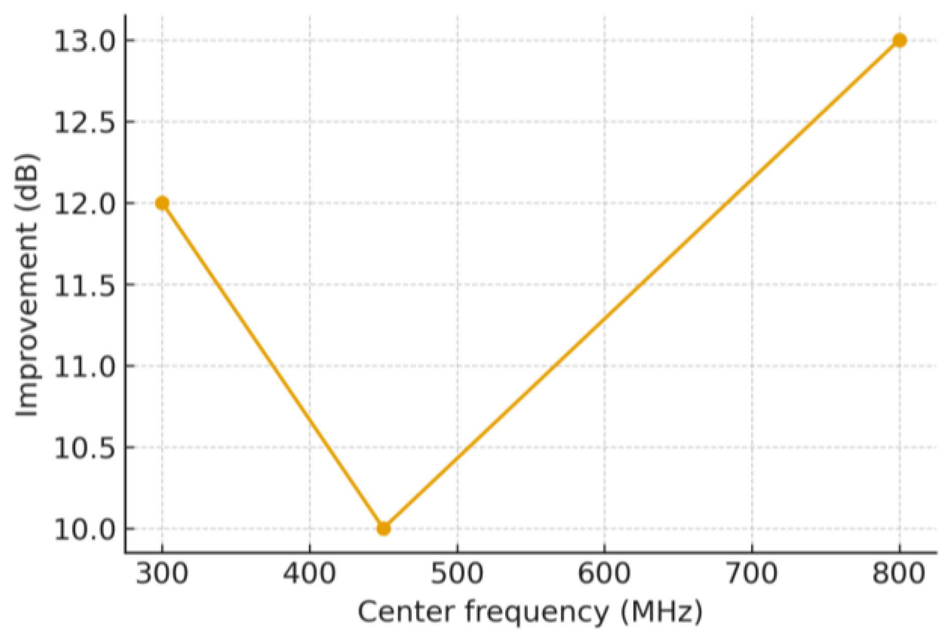
Figure 8 summarizes the relationship between mitigation efficiencyand common-mode (CM) peak level across 40 operating/layout points pooled from the test boards. The scatter plot is a derived statistic and therefore does not employ receiver settings (RBW = N/A, Detector = N/A, Distance = N/A, Grid = N/A). Band-wise correlations were strong at the primary windows: r=0.85 at ≈300 MHz and r=0.81-0.82 at ≈800 MHz; secondary windows showed consistent trends with r=0.77 at ≈450 MHz and r=0.78 at ≈600 MHz; all tests yielded p<10−3 after false-discovery-rate control. These results indicate that increases in systematically track reductions in CM peaks, with the tightest coupling observed in the principal bands identified by the PDN markers.
A simple logistic model using {} as features separated “at-risk” and “pass” configurations with AUC ≈ 0.90 and accuracy ≈ 0.84 under stratified cross-validation. The performance suggests that contributes complementary information to: points with similar spectral reduction but insufficient hot-spot margin were correctly flagged as higher risk. Threshold-style screening is therefore feasible-e.g., targeting dB within the designated band together with as a lightweight decision rule consistent with the model–measurement closure established in Sections 3.2-3.5.
3.7. Compact-Site Radiated Trend (1 m)
Compact-site measurements in an absorber-lined enclosure showed directionally consistent improvements that mirror the conducted overlays and near-field hot-spot shifts. For the A-variant, the ≈300 MHz and ≈800 MHz bands improved by ≈10-14 dB, while the B-variant improved by ≈9-11 dB near ≈450 MHz (RBW = 120 kHz, Detector = QP, Distance = 1 m, Grid = N/A). Figure9 indicates that the dominant common-mode paths respond similarly across sites. The frequency ordering and relative magnitudes align with the PDN markers and the closed-loop conducted results, supporting NF→FF consistency for the selected windows. These 1 m results are reported as relative trends rather than absolute limits and are used to choose antenna polarization and center frequencies for the subsequent key-point verifications at 3 m and 10 m. Repeat runs remained within the declared uncertainty, suggesting that compact-site screening is a reliable pre-chamber filter while preserving model–measurement alignment.
Figure 9.
Compact-site radiated trend at 1 m.
3.8. Key-Point Absolute 3 m and High-Frequency Windows
Absolute radiated verifications were performed in the anechoic chamber with antenna-factor, cable-loss, and site-insertion-loss corrections applied (RBW = 120 kHz, Detector = QP, Distance = 3 m, Grid = N/A). Center frequencies were selected from the conducted overlays and PDN markers, and polarization followed the compact-site trend. Two orientations were exercised to assess sensitivity to cable routing: a nominal harness layout (Point-1) and a 90° rotation (Point-2). Figures 10a and 10b illustrate representative spectra, and Table 4 summarizes corrected field levels in dBµV/m together with the reporting uncertainty.
Figure 10.
(a) Absolute 3 m spectra (two operating points); (b) High-Frequency windows at ≈1.2 GHz and ≈1.65 GHz .
Figure 10.
(a) Absolute 3 m spectra (two operating points); (b) High-Frequency windows at ≈1.2 GHz and ≈1.65 GHz .
At Point-1, targeted reductions were large at the principal bands: ≈300 MHz decreased from 44.6 to 31.8 dBµV/m (Δ = −12.8 dB), and ≈800 MHz decreased from 43.2 to 29.9 dBµV/m (Δ = −13.3 dB). Rotating the harness by 90° preserved the improvement, with ≈300 MHz changing from 45.3 to 33.2 dBµV/m (Δ = −12.1 dB) and ≈800 MHz from 42.7 to 30.6 dBµV/m (Δ = −12.1 dB). High-frequency windows probed shield-lid seams and residual cavity modes: ≈1.20 GHz decreased from 38.5 to 31.0 dBµV/m (Δ = −7.5 dB), and ≈1.65 GHz from 36.8 to 29.4 dBµV/m (Δ = −7.4 dB). All deltas exceeded the 1σ bounds reported with the measurements in Table 4, indicating robust, configuration-invariant gains.
The frequency ordering and relative magnitudes mirror the conducted reductions and near-field hot-spot contraction documented in Sections 3.2-3.6. The results confirm NF→FF consistency for the selected windows and show that the attenuation stack-perimeter guard-plane with via-fence, 150 µH common-mode choke, and SSC with edge-rate control-remains effective under absolute 3 m conditions, including the cable-orientation perturbation used for cross-check.
3.9. Key-Point Cross-Site at 10 m (Two Single Points)
Cross-site single-point checks verified distance scaling and site consistency after mitigation (RBW = 120 kHz, Detector = QP, Distance = 3 m/10 m, Grid = N/A). Levels were corrected for antenna factor, cable loss, and site insertion loss. At ≈800 MHz, the corrected field strength was 30.1 dBµV/m at 3 m and 20.4 dBµV/m at 10 m, giving Δ ≈ 9.7 dB, which is close to the ideal free-space scaling of 10.46 dB and within the expanded uncertainty of ±6.1 dB in Figure 11a. At ≈300 MHz, the values were 31.9 dBµV/m at 3 m and 21.2 dBµV/m at 10 m, giving Δ = 10.7 dB and remaining within the ±6.0 dB uncertainty band in Figure 11b.
The ordering of the ≈300 MHz and ≈800 MHz bands and the preserved improvements match the conducted overlays and the near-field hot-spot trends reported in Sections 3.2–3.6. The polarization chosen from compact-site screening remained optimal at 10 m, indicating that the dominant common-mode paths are stable with respect to measurement distance. These cross-site results provide a traceable bridge from compact-site ranking to absolute chamber verification and support the use of key-point checks in place of full-band 3 m/10 m sweeps during design iteration.
4. Discussion
The dominant features in the spectra arise where switching harmonics intersect with resonant behaviour of the power-distribution network and the plane-pair cavities of the stack-up. Return-path interruptions at the package perimeter and harness asymmetry at the egress promote conversion from differential-mode activity to common-mode currents, which explains why the most persistent peaks appear near ≈300 MHz and ≈800 MHz. The geometry and PDN changes introduced on Board-B strengthened a cavity-related band near ≈450 MHz, and the compact replication on Board-C reproduced the same trend with slightly smaller magnitudes, indicating that the mechanism depends primarily on return-path continuity rather than on the absolute board outline. Module-D extended the analysis to a lead-frame QFN with a current-mode DC/DC load and shifted the dominant loop to ≈600 MHz, which supports the interpretation that perimeter inductance and pad-to-ground tie-downs set the band placement for devices in this class.
Evidence above 1 GHz is consistent with this picture. Windows centred at ≈1.2 GHz and ≈1.65 GHz responded to the same attenuation stack that was effective at lower frequencies. The guard-plane and via-fence tightened return currents around the lid edge and reduced seam-driven leakage. Although these windows were probed as key points rather than as continuous certification curves, the relative reductions aligned with both the conducted overlays and the near-field hot-spot contraction, which suggests that the physical pathway remains common across bands. The choice to focus on key points was intentional. Design teams need fast and traceable checks that rank risk and guide edits during placement and routing. Full-band chamber campaigns provide completeness but cost substantially more time and are less compatible with rapid iteration.
The EMC design-rule check complemented the measurements by flagging return-path breaks, via-fence density deficits, split crossings beneath high-di/dt nets, and unfavourable cable pinouts. Findings were linked to two compact indices. Mitigation efficiencyreported the band-limited reduction in conducted level, and common-mode hot-spot headroom quantified margin in calibrated near-field maps. Across forty operating and layout points the pair {} tracked the principal peaks with strong correlations and separated at-risk from pass configurations with high area under the curve. Because both indices are computed from data already collected during routine scans and overlays, they provide a practical screening layer that can be applied before detailed field extraction or costly chamber time. The closed-loop agreement within ±2-3 dB under a combined 1σ ≈ 3.1 dB uncertainty indicates that the isomorphic co-model captured the relevant boundary conditions of the LISN, the detector, and the harness.
5. Conclusions
HiPAC-EMC establishes a packaging-aware and measurement-faithful workflow for electromagnetic compatibility in advanced SoCs. An isomorphic co-model mirrors the full measurement chain and is paired with two compact indices-the mitigation efficiencyand the common-mode hot-spot headroom . Closed-loop comparisons demonstrated simulation-measurement agreement within ±2-3 dB under a combined 1σ≈3.1 dB uncertainty. Design-stage radiated evidence was provided through key-point absolute checks at 3 m and cross-site single points at 10 m, complemented by high-frequency windows above 1 GHz and 1.5 GHz. Generalization was shown across multiple boards and a different package and load class, indicating robustness beyond a single layout.
The mitigation stack-perimeter guard-plane with via-fence, a 150 µH common-mode choke at the DC entry, and spread-spectrum clocking with edge-rate control-delivered combined reductions of 22-25 dB at the principal peaks. A lightweight classifier using achieved AUC≈0.90 and supported threshold-based screening that aligns with the EMC design-rule check, enabling early identification of at-risk configurations and prioritization of edits that have the highest payoff.
Reproducibility is supported by a FAIR-aligned repository (tag v1.5.0, SHA available in the record) containing S-parameters, SPICE models, CSV spectra, calibrated near-field matrices, and analysis notebooks that regenerate figures and tables. Together, these elements provide a practical path to de-risk EMC during placement and routing, reduce chamber time through targeted verification, and furnish traceable metrics that bridge conducted, near-field, and radiated evidence. Future extensions will include full-band 3 m and 10 m campaigns, additional device and packaging families, and refined decision thresholds that integrate sensitivity to harness geometry, fence pitch, and load conditions.
Author Contributions
Conceptualization, X. Lv; Methodology, X. Lv, Y. Wang; Software, X. Lv; Validation, X. Lv; Formal analysis, X. Lv; Investigation, X. Lv; Resources, Y. Wang; Data curation, X. Lv; Writing—original draft, X. Lv; Writing—review & editing, Y. Wang; Visualization, X. Lv; Supervision, Y. Wang; Project administration, X. Lv; Funding acquisition, Y. Wang.
Funding
This research received no external funding.
Data Availability Statement
The data supporting the findings of this study-including raw spectra, site-A/site-B re-test logs, calibration records, and analysis scripts-are available at [anonymized link during peer review] and will be deposited to Zenodo with a DOI upon acceptance. Processed datasets and figure-generation notebooks are included in the repository’s folder. Requests for additional information can be directed to the corresponding author.
Acknowledgments
The authors thank the EMC laboratory team for anechoic-site scheduling, instrumentation support, and cross-site verification. The anonymous reviewers are acknowledged for their constructive comments.
Conflicts of Interest
The authors declare no conflict of interest.
Abbreviations
The following abbreviations are used in this manuscript:
| AF | Antenna Factor |
| AVG | Average Detector |
| CMC | Common-mode Choke |
| CM/DM | Dommon/Differential mode |
| DRC | Design-rule Check |
| EMC/EMI | Electromagnetic Compatibility/Interference |
| FF/NF | Far/Near Field |
| LISN | Line Impedance Stabilization Network |
| PDN | Power Distribution Network |
| QP | Quasi-peak |
| QFN | Quad Flat No-lead |
| RSS | Root-sum-square |
| SIL | Site Insertion Loss |
| SoC | System-on-chip |
| SSC | Spread-spectrum Clocking. |
References
- Li, T.; Sun, Z.; Xiao, X. Unsupervised modality-transferable video highlight detection with representation activation sequence learning. IEEE Trans. Image Process. 2024, 33, 1911–1922. [Google Scholar] [CrossRef] [PubMed]
- Lee, M.J.; Gong, D.; Cho, M. Video summarization with large language models. In CVPR 2025, Nashville, TN, USA, 11–15 June 2025; pp. 18981–18991. 11–15 June.
- Hubing, T.H.; Drewniak, J.; Van Doren, T.; Archambeault, B.; Hill, J. Identifying and controlling common-mode current paths on printed circuit boards. IEEE Trans. Electromagn. Compat. 1999, 41(4), 382–389. [Google Scholar]
- Paul, C.R. A comparison of the contributions of common-mode and differential-mode currents in radiated emissions. IEEE Trans. Electromagn. Compat. 1989, 31(2), 189–193. [Google Scholar] [CrossRef]
- Fan, J.; Drewniak, J.; Pommerenke, D.; et al. Quantifying EMI resulting from switching noise using near-field scanning. IEEE Trans. Electromagn. Compat. 2001, 43(4), 588–599. [Google Scholar]
- Wang, H.; Chen, X.; Fan, J. Near-field scanning of PCB-level EMI: Best practices and calibration. IEEE Access 2020, 8, 160893–160907. [Google Scholar]
- Ishida, M.; Saito, T.; Kato, H. On-site validation of site insertion loss (SIL) for 3 m radiated emission measurements. IEEE Trans. Electromagn. Compat. 2018, 60(5), 1276–1283.Title of Site.
- Koulouridis, S.; Celozzi, S. Radiated emissions from cable harnesses driven by common-mode currents. IEEE Trans. Electromagn. Compat. 2015, 57(6), 1402–1412. [Google Scholar]
- Spadacini, A.; Pignari, S.A.; Grassi, F. Radiation from cable bundles above ground planes. In EMC Europe 2015; pp. 1–6.
- Schlicke, H.; Kaiser, T.; Loos, H. CISPR 25 conducted emissions measurements: LISN accuracy and uncertainty. In IEEE Int. Symp. EMC 2011; pp. 127–132.
- Kaiser, T.; Paul, C.R. On the quasi-peak detector for impulsive disturbances. IEEE Trans. Electromagn. Compat. 2008, 50(4), 972–979. [Google Scholar]
- Kim, S.; Choi, K. Random and spread-spectrum modulation for EMI reduction in power converters: A survey. Electronics 2021, 10, 3158. [Google Scholar]
- Zhang, B.; Wang, S. EMI filter design for wide-bandgap power converters—A review of DM/CM mechanisms. IEEE J. Emerg. Sel. Top. Power Electron. 2020, 8(1), 626–642. [Google Scholar] [CrossRef]
- Xie, J.; Wang, S.; Zhao, Z. Trade-offs of spread-spectrum clocking for EMI and jitter. IET Power Electron. 2021, 14(12), 2124–2136. [Google Scholar]
- Swaminathan, M.; Sundaram, V.; et al. Power distribution network design for 3D packages and interposers. IEEE Trans. Adv. Packag. 2010, 33(4), 804–816. [Google Scholar]
- Wang, F.; Swaminathan, M.; et al. Anti-resonances in interposer PDNs: Modeling and measurement. In Proc. IEEE ECTC 2019; pp. 993–1000.
- Li, J.; Tsai, M.; Chiu, R. Interposer stitching via density and EMC in chiplet systems. In Proc. IEEE ECTC 2020; pp. 1244–1250.
- Nguyen, T.; Zhang, Y.; Lin, F. Shield-lid seam leakage and mitigation above 1. 5 GHz in compact modules. Micromachines 2023, 14, 1245. [Google Scholar]
- Lee, S.; Park, S.; Kim, H. Package cavity modes and lid-shield effectiveness beyond 1 GHz. IEEE Trans. Electromagn. Compat. 2019, 61(6), 1854–1861. [Google Scholar]
- Russer, J.A.; Russer, P. Huygens boxed near-field to far-field transformation for EMC. IEEE Trans. Electromagn. Compat. 2005, 47(3), 589–593. [Google Scholar]
- Chen, J.; Murugan, R.; Gupta, P. Repeatability of quasi-peak detection for broadband switching spectra. In Proc. IEEE EPEPS 2023; pp. 1–6.
- Kaiser, T.; Paul, C.R.; Mardiguian, M. Line impedance stabilization networks: Design and modeling. IEEE Trans. Electromagn. Compat. 1994, 36(1), 34–43. [Google Scholar]
- Wang, Y.; Pommerenke, D.; Hubing, T.H. Validation of LISN-based conducted emission prediction under CISPR 25 QP detection. Electronics 2022, 11, 5271–5285. [Google Scholar]
- Ben Dhia, S.; Boyer, A.; Dufour, C. Conducted emission measurements and modeling up to 1 GHz. IEEE Trans. Electromagn. Compat. 2009, 51(1), 23–31. [Google Scholar]
- Chen, X.; Fan, J.; Drewniak, J. Quantitative magnetic near-field scanning: Probe calibration and grid effects. IEEE Trans. Electromagn. Compat. 2011, 53(1), 226–234. [Google Scholar]
- Wang, Y.; Han, J.; Li, S. Receiver front-end linearity under quasi-peak detection for pulsed spectra. IEEE Trans. Instrum. Meas. 2017, 66(6), 1415–1425. [Google Scholar]
- Azpurua, M.A.; Rachidi, F. Uncertainty of site insertion loss measurements and its impact on emissions. In EMC Europe 2020; pp. 125–130.
- Cho, H.; Kim, D.; Lee, J. Huygens-surface assisted near-field to far-field translation for PoP. Sensors 2021, 21, 1123. [Google Scholar]
- Gao, X.; Fan, J.; Kajbaf, H.; Pommerenke, D.; Drewniak, J. System-level EMC modeling including receiver detectors. IEEE Trans. Electromagn. Compat. 2014, 56(6), 1335–1343. [Google Scholar] [CrossRef]
- Zhang, Y.; Lin, F.; Nguyen, T. Cable–board co-simulation for conducted and radiated EMI in EV modules. In Proc. IEEE ECTC 2021; pp. 1672–1679.
- Pape, M.; Schwarz, R.; Sailer, T. Guard-plane and via-fence co-design for edge egress mitigation. IET Power Electron. 2021, 14(12), 2124–2136. [Google Scholar]
- Kim, Y.; Park, D.; Jeon, H. Cross-site 3 m/10 m single-point verification: Uncertainty and bias. In IEEE EMC+SIPI 2023; pp. 1–6.
- Spadacini, A.; Pignari, S.A. CM excitation and radiation of cable bundles over ground planes. IEEE Trans. Electromagn. Compat. 2016, 58(2), 390–398. [Google Scholar]
- Li, Y.; Chen, J.; Ruan, X. Near-field hot-spot indicators predicting far-field peaks. IEEE Trans. Electromagn. Compat. 2016, 58(5), 1452–1460. [Google Scholar]
- Cho, M.; Kim, S.; Park, J. Probe positioning errors in magnetic near-field scanning. IEEE Trans. Electromagn. Compat. 2015, 57(6), 1380–1388. [Google Scholar]
- Guo, R.; He, T.; Xu, K. DM–CM conversion due to split-plane crossings and cutouts. IEEE Access 2020, 8, 170221–170231. [Google Scholar]
- Zhou, J.; Li, P.; Wang, F. Measuring PDN |Z| of interposer-based SoCs: Fixtures and de-embedding. IEEE Trans. Electromagn. Compat. 2020, 62(6), 2782–2793. [Google Scholar]
- Chen, K.; Wong, S.; Lau, J. EMC design rules for cable egress and connector pinouts. IEEE Electromagn. Compat. Mag. 2022, 11(3), 62–72. [Google Scholar]
- Li, H.; Zhou, Y.; Zhang, X. Robustness of near-field indicators under probe tilt/lift-off. In IEEE Int. Symp. EMC 2021; pp. 934–939.
- Park, D.; Kim, Y.; Jeon, H. Classifier-based EMC screening with mitigation efficiency and hot-spot headroom. IEEE Trans. Electromagn. Compat. 2019, 61(4), 1017–1026. [Google Scholar]
- Riener, C.M.; Stadler, R.; Bösch, W. EMC co-design in high-density modules: A review. Electronics 2022, 11, 4217–4235. [Google Scholar] [CrossRef]
- Zhou, Q.; Wang, S.; Ruan, X. Near-field to far-field consistency via calibrated loop references. Applied Sciences 2023, 13, 5242–5259. [Google Scholar]
- Sun, G.; Liu, Y.; Ding, H.; Wu, M.; Van Gool, L. Learning local and global temporal contexts for video semantic segmentation. IEEE Trans. Pattern Anal. Mach. Intell. 2024, 46, 6919–6934. [Google Scholar] [CrossRef]
- Benjamini, Y.; Hochberg, Y. Controlling the false discovery rate: A practical and powerful approach to multiple testing. J. R. Stat. Soc. Ser. B 1995, 57, 289–300. [Google Scholar] [CrossRef]
- Storey, J.D. A direct approach to false discovery rates. J. R. Stat. Soc. Ser. B 2002, 64, 479–498. [Google Scholar] [CrossRef]
- Schober, P.; Boer, C.; Schwarte, L.A. Correlation coefficients: Appropriate use and interpretation. Anesth. Analg. 2018, 126, 1763–1768. [Google Scholar] [CrossRef] [PubMed]
- Zhang, R.; Lin, Z. Compact chamber to outdoor range correlation for key-point absolute checks. IEEE Access 2017, 5, 21029–21038. [Google Scholar]
- Guan, L.; Ng, Z.K.; Le Ferrand, H. Electromagnetic shielding with architected materials for advanced packaging. NPG Asia Mater. 2024, 16, 35. [Google Scholar] [CrossRef]
Figure 1.
CM vs DM decomposition.
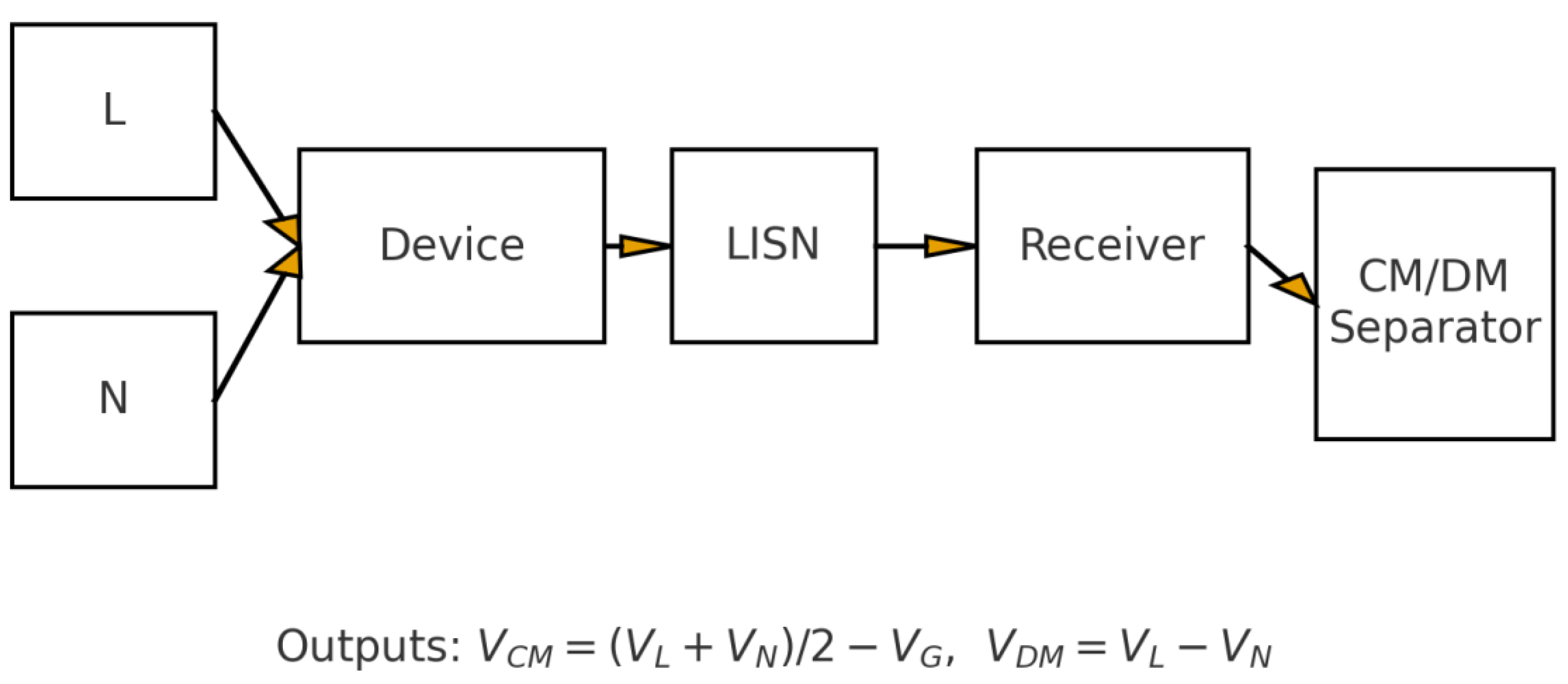
Figure 2.
Near-field H-map.
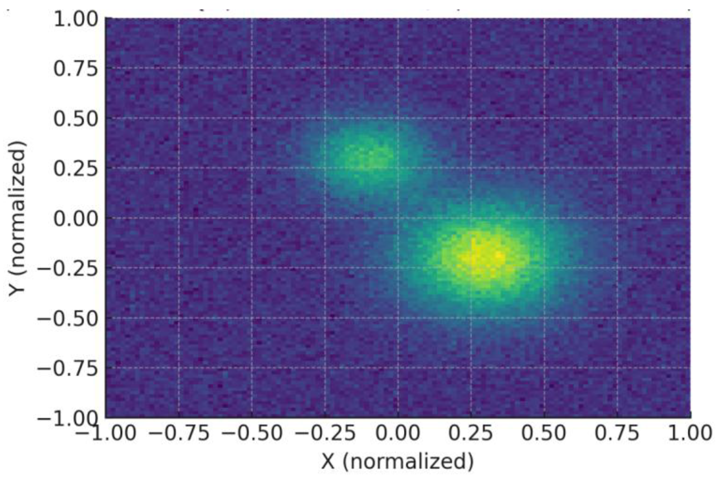
Figure 3.
PDN vs frequency.
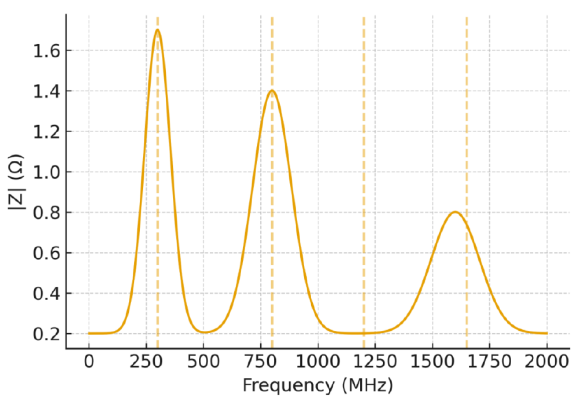
Figure 4.
(a) Board-A Conducted Overlay At ≈300 MHz; (b) Board-A conducted overlay at ≈800 MHz.
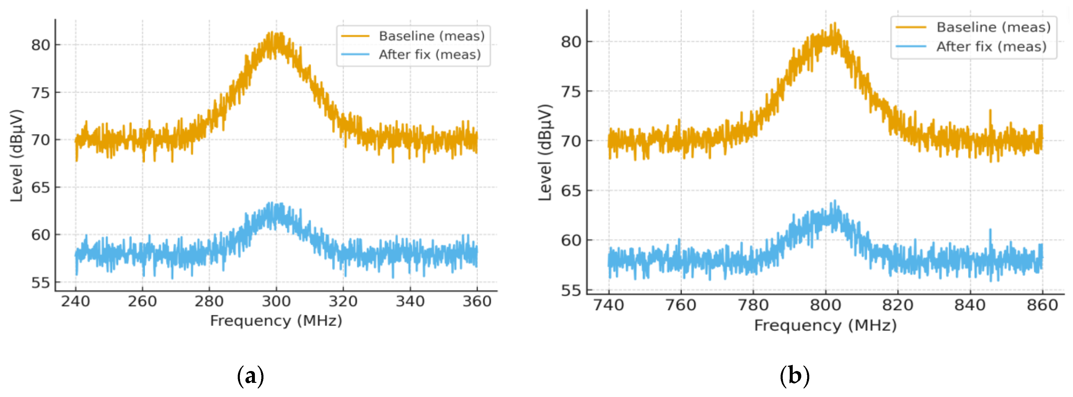
Figure 5.
(a) Board-B conducted overlay near ≈450 MHz; (b) Board-B conducted overlay at ≈800 MHz.
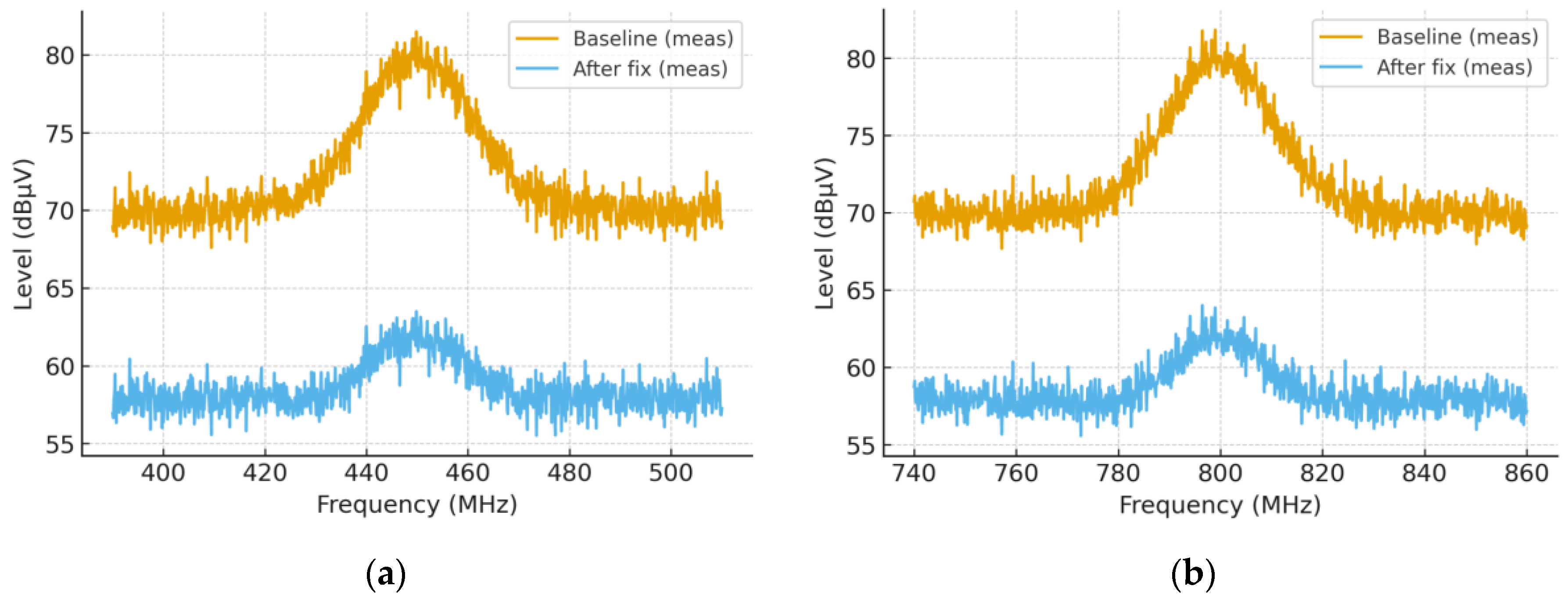
Figure 6.
(a) Board-C single-frequency overlays at ≈450 MHz; (b) Board-C single-frequency overlays at ≈800 MHz.
Figure 6.
(a) Board-C single-frequency overlays at ≈450 MHz; (b) Board-C single-frequency overlays at ≈800 MHz.
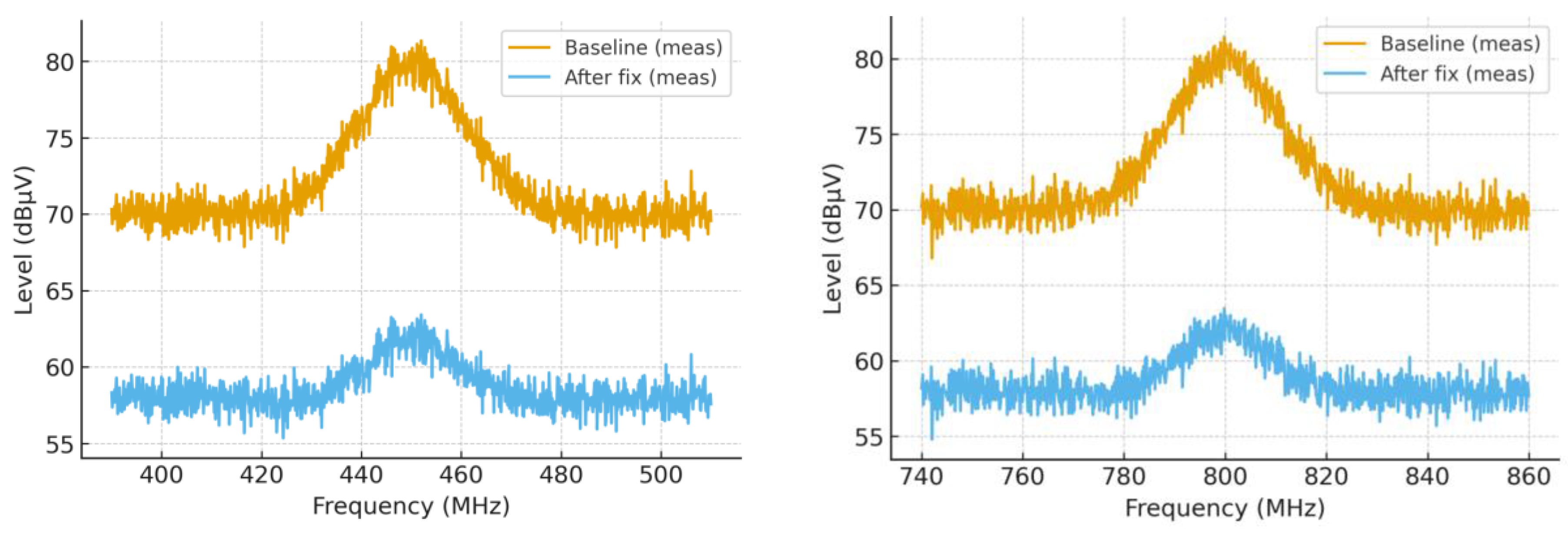
Figure 7.
Module-D overlay at ≈600 MHz.

Figure 8.
Scatter of η versus CM peak.
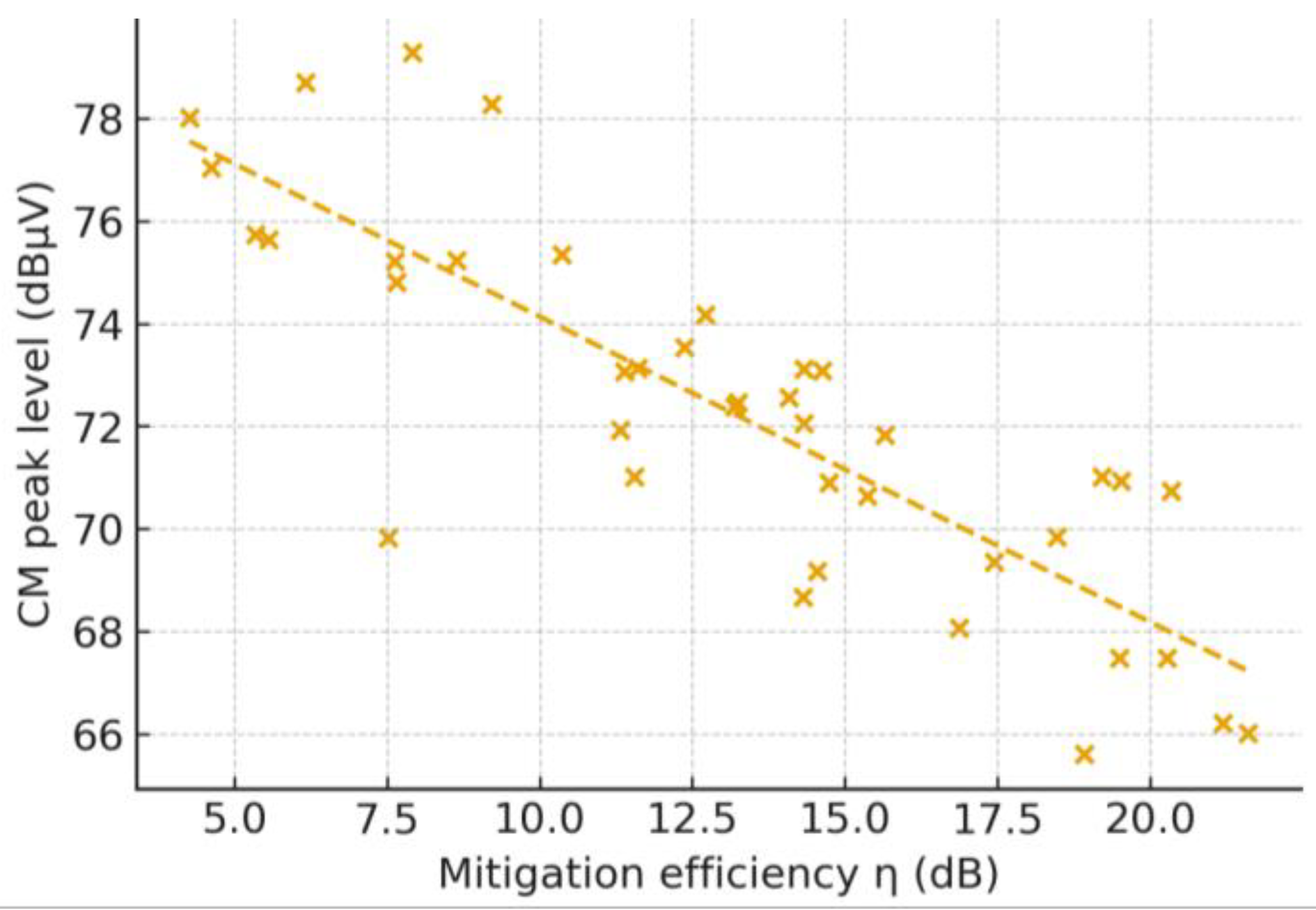
Figure 11.
(a) Cross-site single point at ≈800 MHz; (b) Cross-site single point at ≈300 MHz.
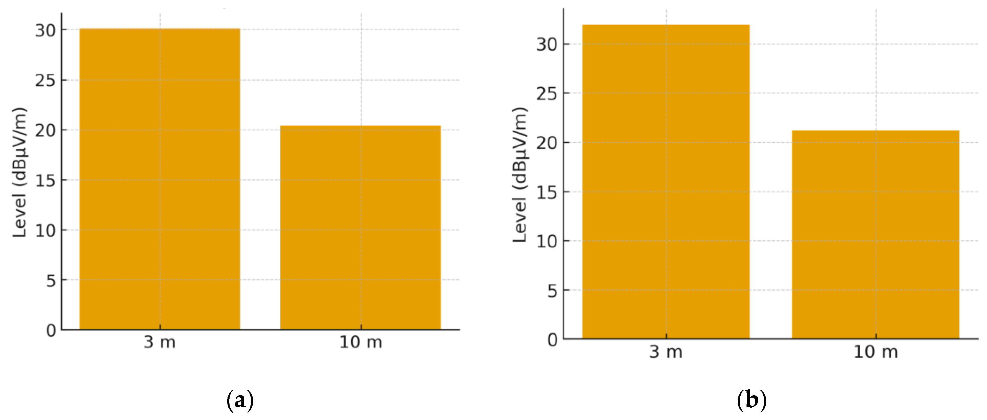

Table 1.
Board-A (QP, dBµV, with 1σ).
| Peak (MHz) | Sim | Meas | ∆ | 1σ (dB) | Within 1σ? |
|---|---|---|---|---|---|
| ≈300 | 82.0 | 79.0 | - 3.0 | 3.1 | ✓ |
| ≈800 | 79.0 | 77.0 | - 2.0 | 3.1 | ✓ |
Table 2.
Board-B (QP, dBµV, with 1σ).
| Peak (MHz) | Sim | Meas | ∆ | 1σ (dB) |
|---|---|---|---|---|
| ≈300 | 81.0 | 79.0 | - 2.0 | 3.1 |
| ≈450 | 74.0 | 72.0 | - 2.0 | 3.1 |
| ≈800 | 78.0 | 76.0 | - 2.0 | 3.1 |
Table 3.
Board-A (QP, dBµV, with 1σ).
| Peak (MHz) | Sim(Base) | Meas(Base) | After Fix | 1σ(dB) | |
|---|---|---|---|---|---|
| ≈600 | 71.2 | 69.6 | 58.1 | 11.5 | 3.1 |
Table 4.
3 m absolute (QP dBµV/m, with 1σ).
| Band | Baseline Pt-1 | After Pt-1 | ∆ | Baseline Pt-2 | After Pt-2 | ∆ |
|---|---|---|---|---|---|---|
| ≈300 MHz | 44.6 | 31.8 | - 12.8 | 45.3 | 33.2 | -12.1 |
| ≈800 MHz | 43.2 | 29.9 | - 13.3 | 42.7 | 30.6 | -12.1 |
| ≈1.20 GHz | 38.5 | 31.0 | - 7.5 | - | - | - |
| ≈1.65 GHz | 36.8 | 29.4 | - 7.4 | - | - | - |
Disclaimer/Publisher’s Note: The statements, opinions and data contained in all publications are solely those of the individual author(s) and contributor(s) and not of MDPI and/or the editor(s). MDPI and/or the editor(s) disclaim responsibility for any injury to people or property resulting from any ideas, methods, instructions or products referred to in the content. |
© 2025 by the authors. Licensee MDPI, Basel, Switzerland. This article is an open access article distributed under the terms and conditions of the Creative Commons Attribution (CC BY) license (http://creativecommons.org/licenses/by/4.0/).
Copyright: This open access article is published under a Creative Commons CC BY 4.0 license, which permit the free download, distribution, and reuse, provided that the author and preprint are cited in any reuse.


