
Submitted:
25 December 2024
Posted:
25 December 2024
You are already at the latest version
Abstract
High switching frequencies in converters significantly reduce the size of passive components, namely inductors and transformers, thus enabling high power density. However, these frequencies also introduce challenges such as semiconductor device reliability, thermal management, magnetic design, and electromagnetic interference. This paper discusses a dc-dc converter operating at 1 MHz and its associated design challenges. The relationship between GaN device on-resistance, junction temperature and losses in scenarios where the converter operates beyond its nominal design specifications is analyzed. Additionally, a PCB-based inductor is fully characterized and the parasitic effects of PCB traces are examined for a 1-MHz, 1-kW application. Finally, conducted and radiated emissions of the converter are addressed supported by simulation and hardware experimental measurements.
Keywords:
1. Introduction
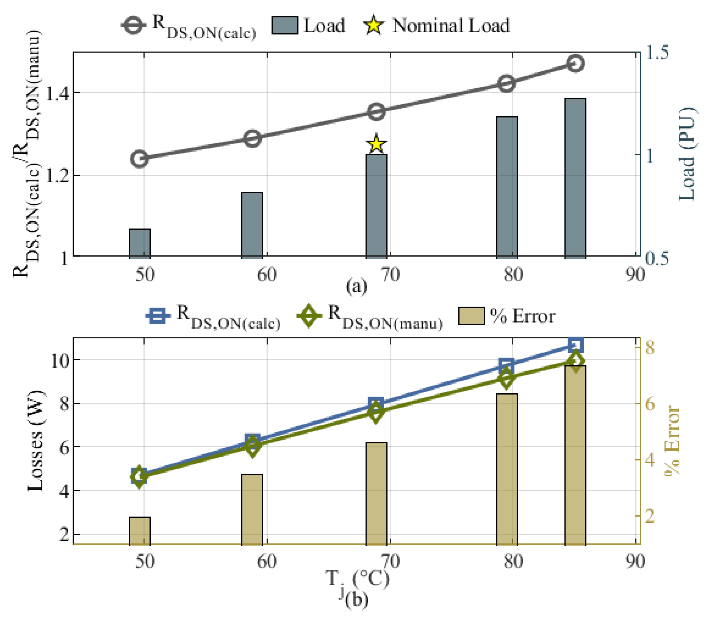
- A linear fit equation is proposed to accurately quantify the dynamic on-resistance of GaN HEMT device in relation to both losses and .
- Characterization of a PCB-based inductor designed for a 1-MHz, 1-kW application with emphasis on core material selection and the minimization of parasitic effects, and
- conducted and radiated EMI tests for a MHz converter were performed and include both simulation and hardware results.
2. GaN HEMT Dynamic On-Resistance ()
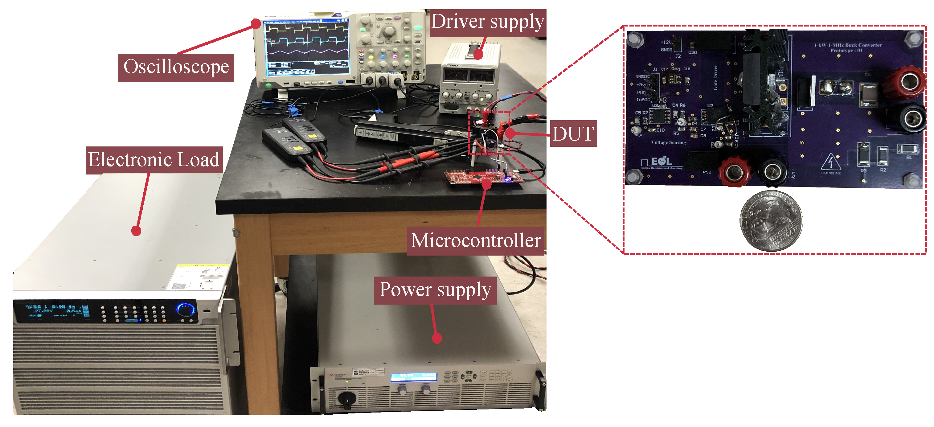
2.1. Methodology
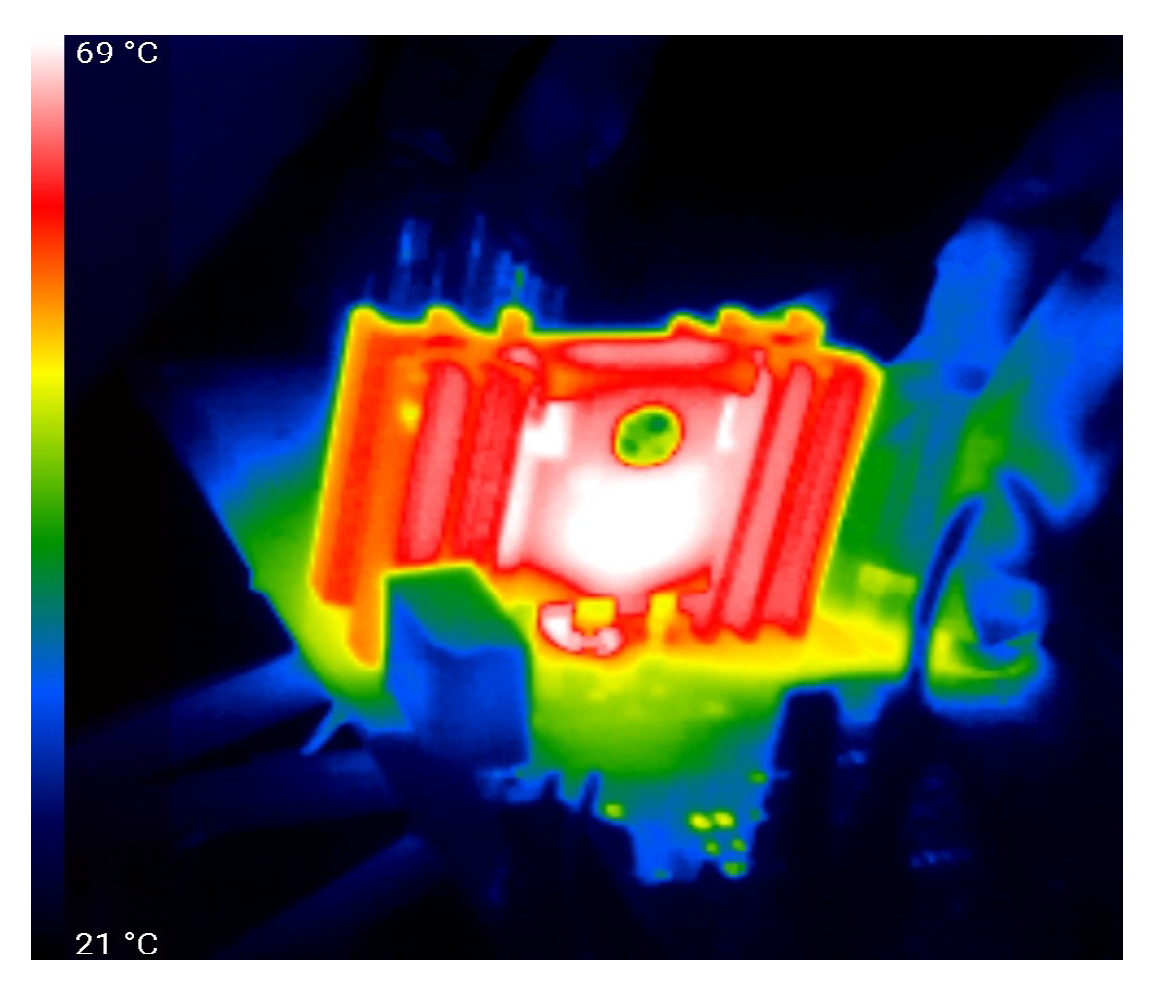
2.2. Experimental Results
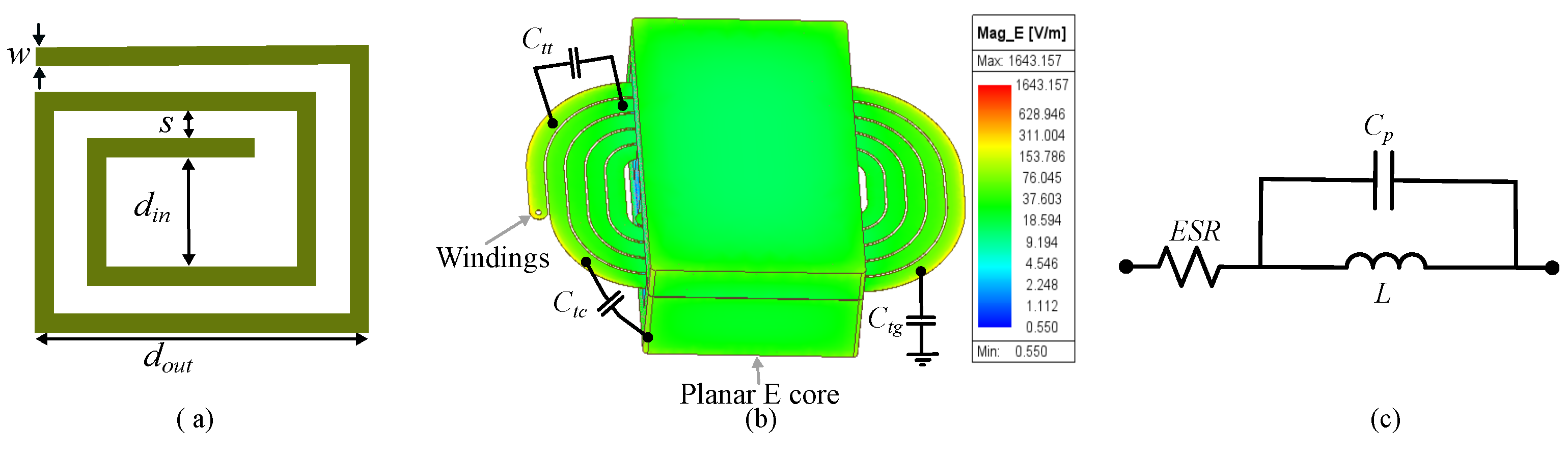
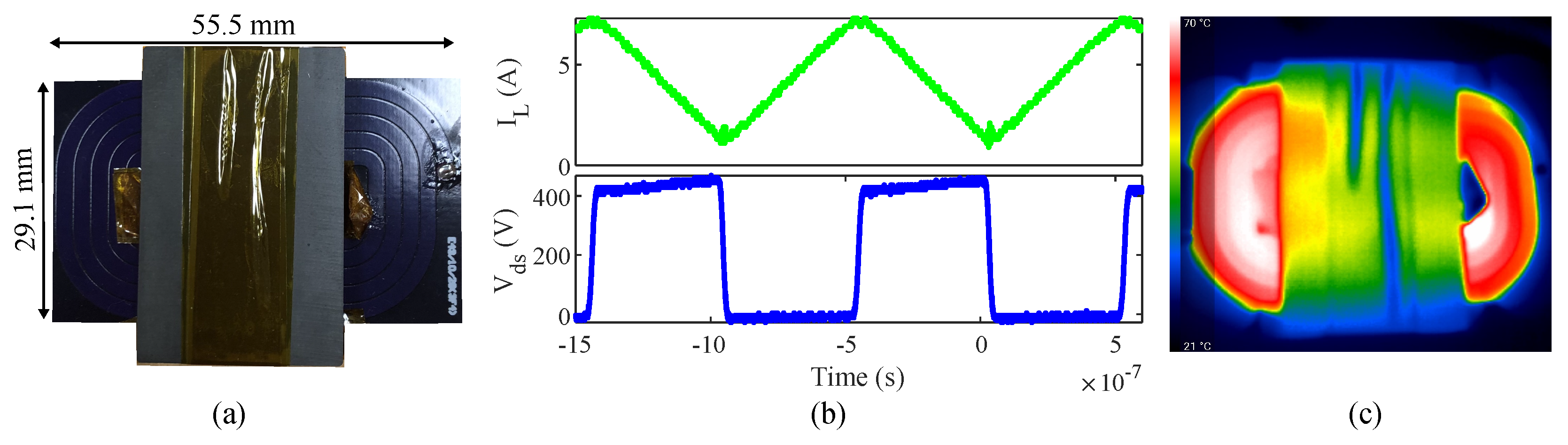
3. PCB-Based Inductor
3.1. Core Material and Design Specs
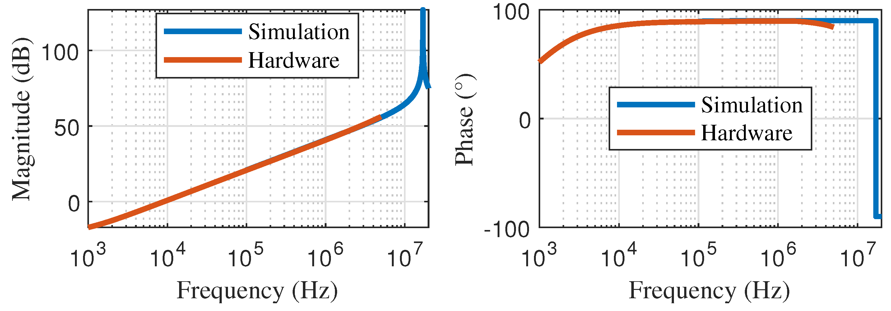
3.2. Parasitic Capacitance and Characterization
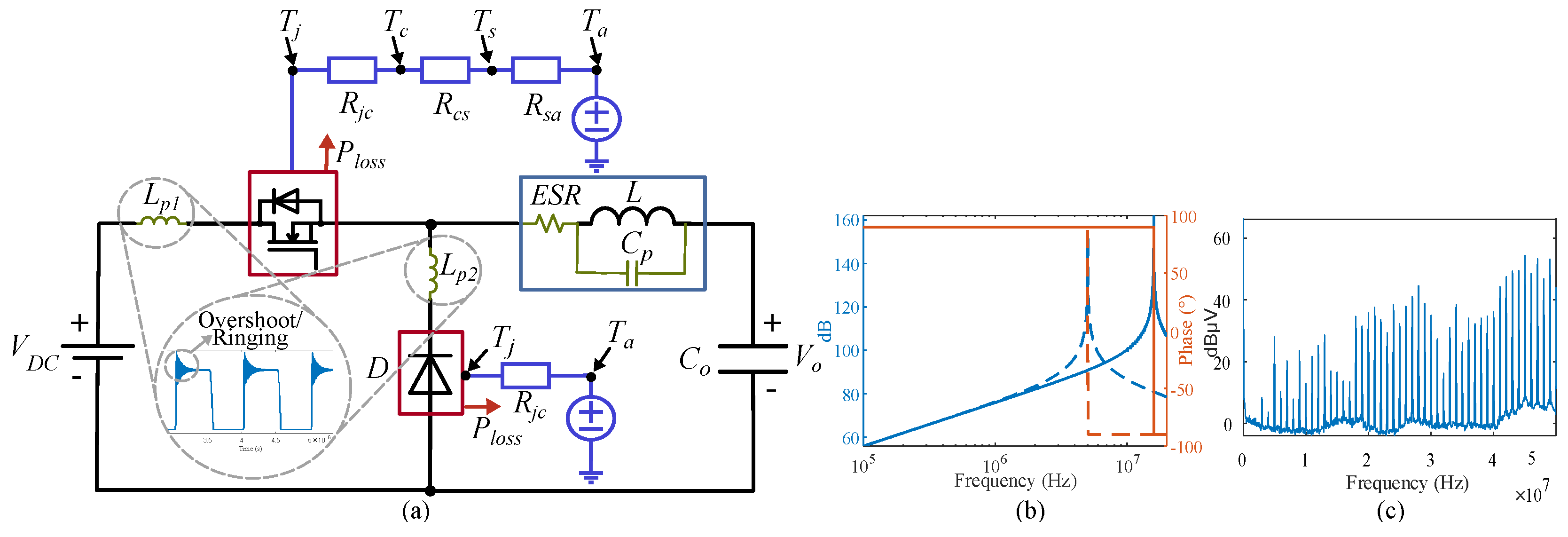
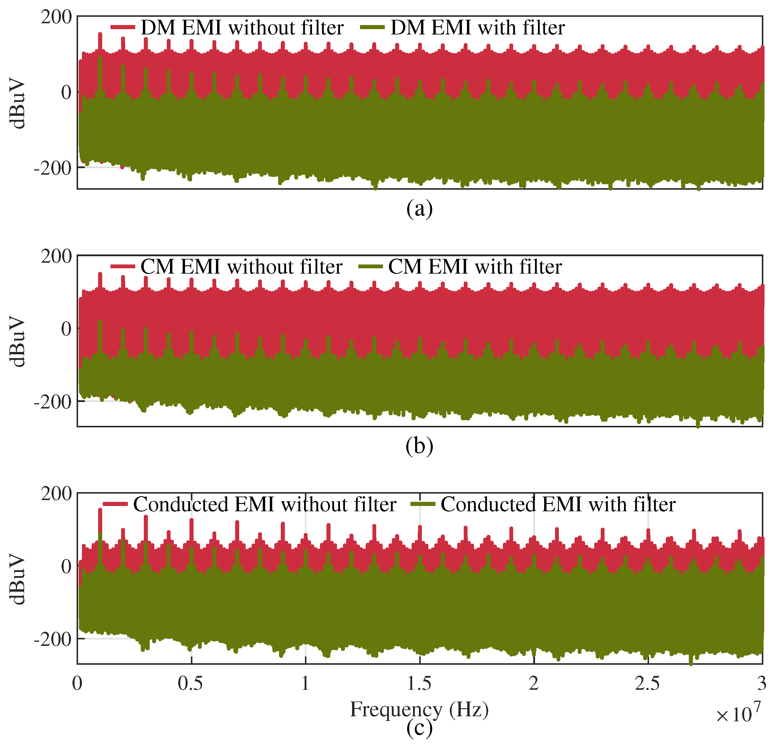
4. Electromagnetic Interference (EMI)
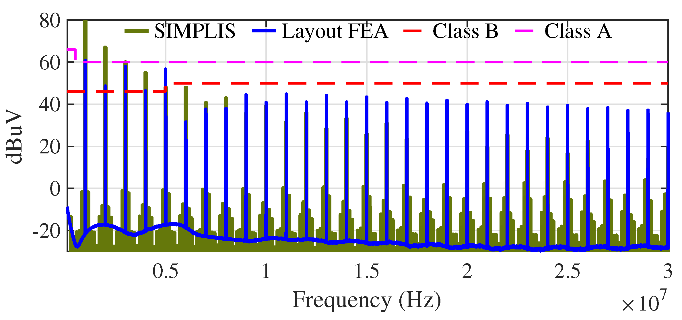
4.1. Conducted EMI
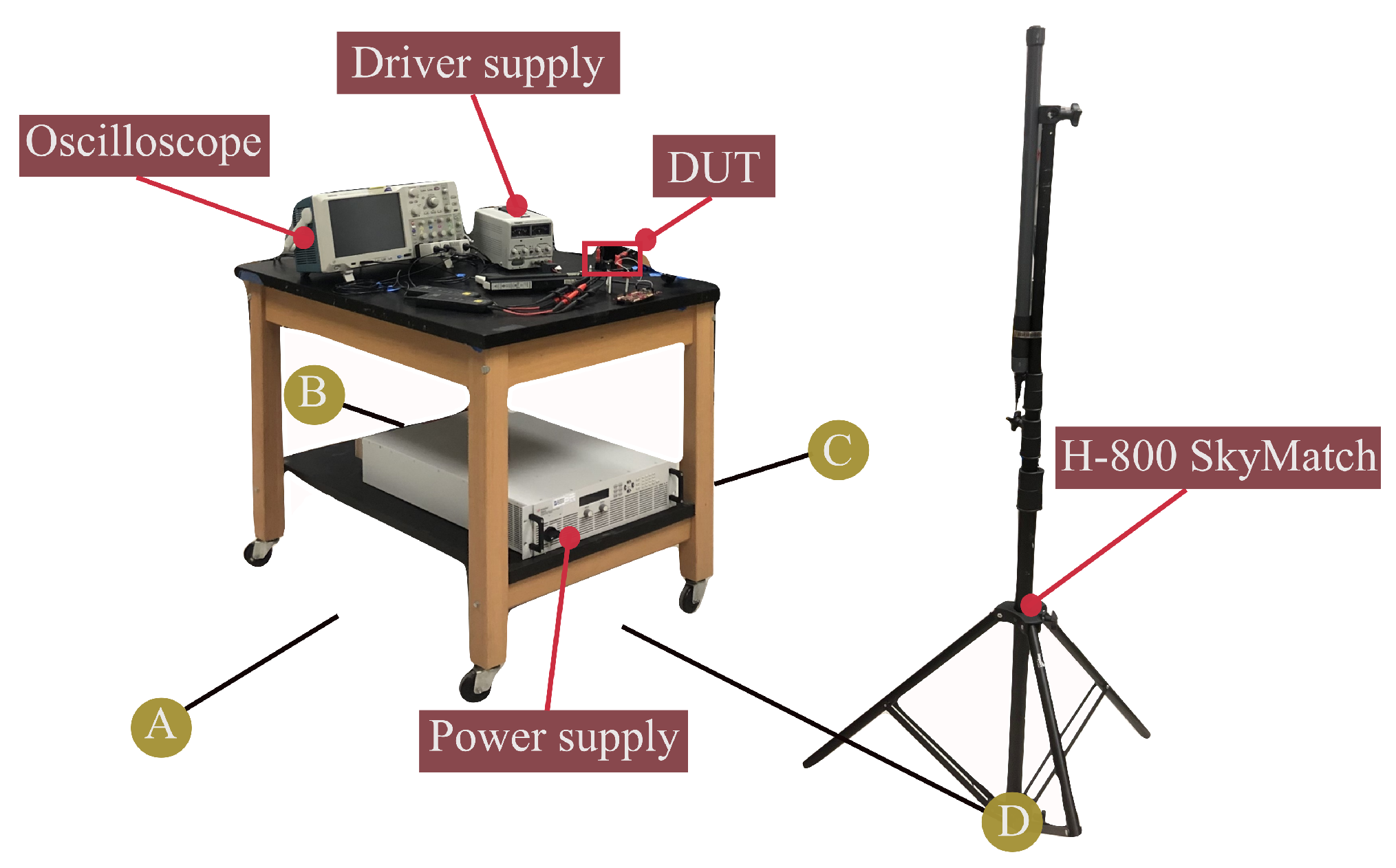
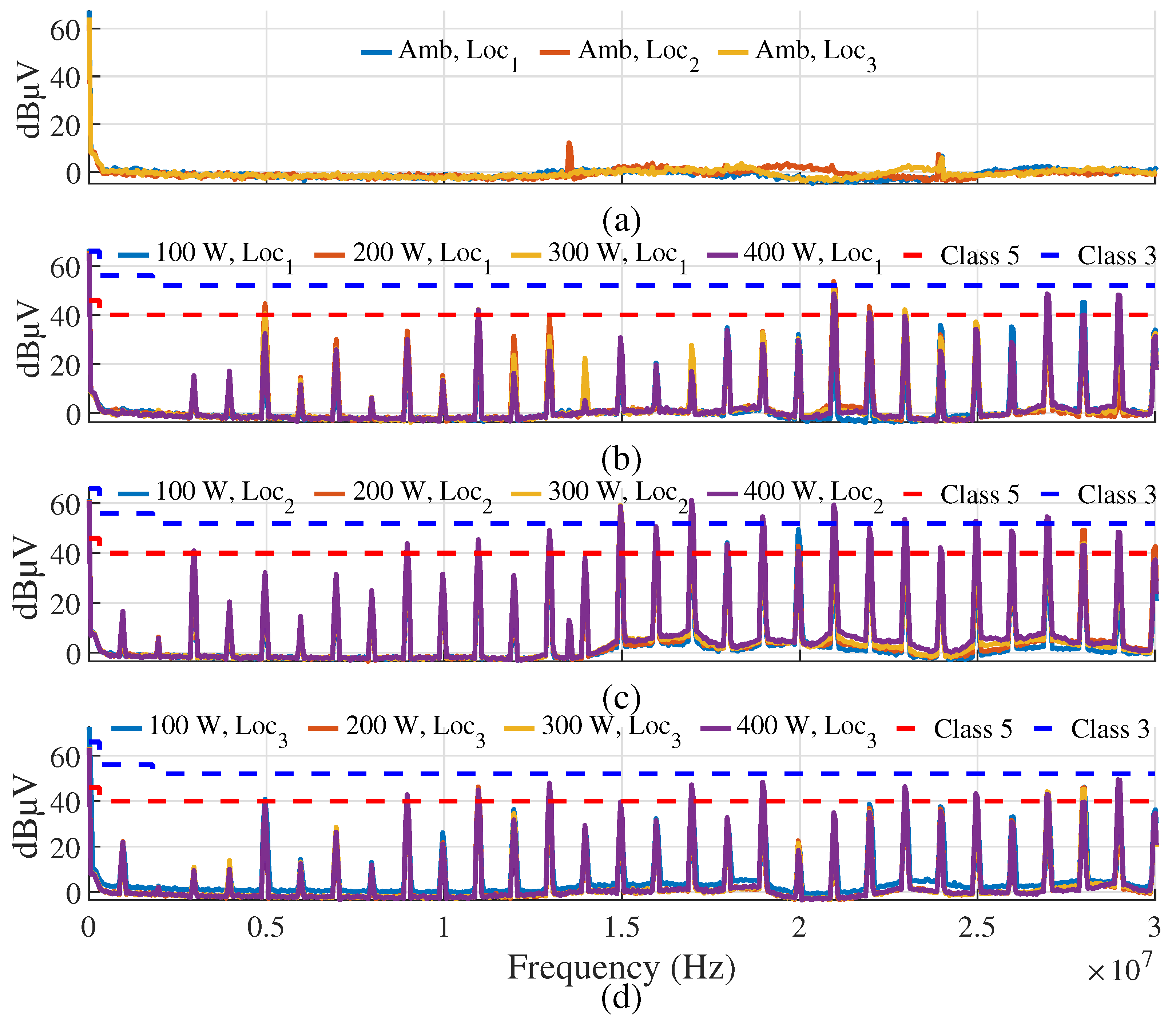
4.2. Radiated EMI
5. Conclusions
Author Contributions
Funding
Data Availability Statement
Conflicts of Interest
References
- Menzi, D.; Imperiali, L.; Bürgisser, E.; Ulmer, M.; Huber, J.; Kolar, J.W. Ultra-Lightweight High-Efficiency Buck-Boost DC-DC Converters for Future eVTOL Aircraft with Hybrid Power Supply. IEEE Transactions on Transportation Electrification 2024, pp. 1–1. [CrossRef]
- Mahdi, H.; Hoff, B.; Østrem, T. A Review of Power Converters for Ships Electrification. IEEE Transactions on Power Electronics 2023, 38, 4680–4697. [Google Scholar] [CrossRef]
- Kim, I.; Park, J.W. Multifunctional Integrated DC–DC Converter for Electric Vehicles. IEEE Transactions on Power Electronics 2024, 39, 7252–7263. [Google Scholar] [CrossRef]
- Hussain, A.; Perez, D.; Cucak, D.; Booth, K. PCB-Based Inductor Design for 1-kW, 1-MHz Buck Converter. In Proceedings of the 2024 IEEE Applied Power Electronics Conference and Exposition (APEC); 2024; pp. 3199–3203. [Google Scholar] [CrossRef]
- Booth, K.; Subramanyan, H.; Liang, X.; Liu, J.; Srdic, S.; Lukic, S. Optimization of Medium Frequency Transformers with Practical Considerations. In Proceedings of the 2019 IEEE Applied Power Electronics Conference and Exposition (APEC); 2019; pp. 2906–2911. [Google Scholar] [CrossRef]
- Mazumder, S.K.; Voss, L.F.; Dowling, K.M.; Conway, A.; Hall, D.; Kaplar, R.J.; Pickrell, G.W.; Flicker, J.; Binder, A.T.; Chowdhury, S.; et al. Overview of Wide/Ultrawide Bandgap Power Semiconductor Devices for Distributed Energy Resources. IEEE Journal of Emerging and Selected Topics in Power Electronics 2023, 11, 3957–3982. [Google Scholar] [CrossRef]
- Gao, Y.; Sankaranarayanan, V.; Dede, E.M.; Zhou, Y.; Zhou, F.; Erickson, R.W.; Maksimovi´c, D. Modeling and Design of High-Power, High-Current-Ripple Planar Inductors. IEEE Transactions on Power Electronics 2022, 37, 5816–5832. [Google Scholar] [CrossRef]
- Fan, W.; Shi, Y.; Chen, Y. A Method for CM EMI Suppression on PFC Converter Using Lossless Snubber with Chaotic Spread Spectrum. Energies 2023, 16. [Google Scholar] [CrossRef]
- Iannaccone, G.; Sbrana, C.; Morelli, I.; Strangio, S. Power Electronics Based on Wide-Bandgap Semiconduc-tors: Opportunities and Challenges. IEEE Access 2021, 9, 139446–139456. [Google Scholar] [CrossRef]
- Kozak, J.P.; Zhang, R.; Porter, M.; Song, Q.; Liu, J.; Wang, B.; Wang, R.; Saito, W.; Zhang, Y. Stability, Reliability, and Robustness of GaN Power Devices: A Review. IEEE Transactions on Power Electronics 2023, 38, 8442–8471. [Google Scholar] [CrossRef]
- Yuan, M.; Niroula, J.; Xie, Q.; Rajput, N.S.; Fu, K.; Luo, S.; Das, S.K.; Iqbal, A.J.B.; Sikder, B.; Isamotu, M.F.; et al. Enhancement-Mode GaN Transistor Technology for Harsh Environment Operation. IEEE Electron Device Letters 2023, 44, 1068–1071. [Google Scholar] [CrossRef]
- Qin, H.; Peng, J.; Zhang, Z.; Zhang, F.; Zhao, X.; Xu, Z. Junction temperature prediction method of GaN HEMT power devices based on accurate on-voltage testing. Energy Reports 2023, 9, 389–395. [Google Scholar] [CrossRef]
- Yan, D.; Ma, D.B. Online Condition Monitoring for GaN Power Devices With Integrated Dynamic On-Resistance Full Profile Scan and Offset Calibration. IEEE Transactions on Power Electronics 2024, 39, 6215–6224. [Google Scholar] [CrossRef]
- Li, S.; Ma, Y.; Zhang, C.; Lu, W.; Liu, M.; Li, M.; Yang, L.; Liu, S.; Wei, J.; Zhang, L.; et al. Physics-Based SPICE Modeling of Dynamic on-State Resistance of p-GaN HEMTs. IEEE Transactions on Power Electronics 2023, 38, 7988–7992. [Google Scholar] [CrossRef]
- Li, K.; Videt, A.; Idir, N.; Evans, P.L.; Johnson, C.M. Accurate Measurement of Dynamic on-State Resistances of GaN Devices Under Reverse and Forward Conduction in High Frequency Power Converter. IEEE Transactions on Power Electronics 2020, 35, 9650–9660. [Google Scholar] [CrossRef]
- Nabih, A.; Jin, F.; Gadelrab, R.; Lee, F.C.; Li, Q. Characterization and Mitigation of Dimensional Effects on Core Loss in High-Power High-Frequency Converters. IEEE Transactions on Power Electronics 2023, 38, 14017–14036. [Google Scholar] [CrossRef]
- Saket, M.A.; Shafiei, N.; Ordonez, M. LLC Converters With Planar Transformers: Issues and Mitigation. IEEE Transactions on Power Electronics 2017, 32, 4524–4542. [Google Scholar] [CrossRef]
- Chafi, A.; Idir, N.; Videt, A.; Maher, H. Design Method of PCB Inductors for High-Frequency GaN Converters. IEEE Transactions on Power Electronics 2021, 36, 805–814. [Google Scholar] [CrossRef]
- Luan, S.; Munk-Nielsen, S.; Yan, Z.; Schupp, J.; Wakelin, B.; Hortans, M.; Zhao, H. Design Guidelines to Reduce Parasitic Capacitance in Planar Inductors. In Proceedings of the 2023 IEEE Applied Power Electronics Conference and Exposition (APEC); 2023; pp. 1579–1585. [Google Scholar] [CrossRef]
- Wang, S.; Pham, P.H.; Li, Q.; Nabih, A.; Prakash, P.R. PCB Winding-Based Coupled Inductor for a High-Frequency DC/DC Converter with 99In Proceedings of the 2023 IEEE Applied Power Electronics Conference and Exposition (APEC), 2023, pp. 420–425. [Google Scholar] [CrossRef]
- Yu, Z.; Yang, X.; Wei, G.; Zhou, Y.; Xiao, Y.; Qin, M.; Wu, J.; Wang, K.; Chen, W.; Wang, L. A Novel Pyramid Winding for PCB Planar Inductors With Fewer Copper Layers and Lower AC Copper Loss. IEEE Transactions on Power Electronics 2022, 37, 11461–11468. [Google Scholar] [CrossRef]
- Ma, Z.; Wang, S.; Huang, Q.; Yang, Y. A Review of Radiated EMI Research in Power Electronics Systems. IEEE Journal of Emerging and Selected Topics in Power Electronics 2024, 12, 675–694. [Google Scholar] [CrossRef]
- Tarateeraseth, V. Educational laboratory experiments on EMC in power electronics. IEEE Electromagnetic Compatibility Magazine 2014, 3, 55–60. [Google Scholar] [CrossRef]
- Yao, J.; Lai, Y.; Ma, Z.; Wang, S. Advances in Modeling and Reduction of Conducted and Radiated EMI in Non-isolated Power Converters. In Proceedings of the 2021 IEEE Applied Power Electronics Conference and Exposition (APEC); 2021; pp. 2305–2312. [Google Scholar] [CrossRef]
- Ma, Z.; Lai, Y.; Yang, Y.; Huang, Q.; Wang, S. Review of Radiated EMI Modeling and Mitigation Techniques in Power Electronics Systems. In Proceedings of the 2023 IEEE Applied Power Electronics Conference and Exposition (APEC); 2023; pp. 1776–1783. [Google Scholar] [CrossRef]
- Persson, E. Optimizing PCB Layout for HV GaN Power Transistors. IEEE Power Electronics Magazine 2023, 10, 65–78. [Google Scholar] [CrossRef]
- Sun, B.; Burgos, R.; Boroyevich, D. Common-Mode EMI Unterminated Behavioral Model of Wide-Bandgap-Based Power Converters Operating at High Switching Frequency. IEEE Journal of Emerging and Selected Topics in Power Electronics 2019, 7, 2561–2570. [Google Scholar] [CrossRef]
- Yao, J.; Lai, Y.; Ma, Z.; Wang, S. Investigation of Noise Spectrum and Radiated EMI in High Switching Frequency Flyback Converters. In Proceedings of the 2021 IEEE Applied Power Electronics Conference and Exposition (APEC); 2021; pp. 2265–2270. [Google Scholar] [CrossRef]
- Tiwari, S.; Basu, S.; Undeland, T.M.; Midtgård, O.M. Efficiency and Conducted EMI Evaluation of a Single-Phase Power Factor Correction Boost Converter Using State-of-the-Art SiC Mosfet and SiC Diode. IEEE Transactions on Industry Applications 2019, 55, 7745–7756. [Google Scholar] [CrossRef]
- Chen, H.; Hu, Y.; Wang, L.; Zhang, Z.; Chen, G. EMI Filter Design Based on High-Frequency Modeling of Common-mode Chokes. In Proceedings of the 2018 IEEE 27th International Symposium on Industrial Electronics (ISIE); 2018; pp. 384–388. [Google Scholar] [CrossRef]
- Ishii, Y.; Nagasawa, S.; Horiguchi, T.; Mukunoki, Y.; Jimichi, T.; Kuzumoto, M.; Hagiwara, M. Accurate Conducted EMI Simulation of a Buck Converter With a Compact Model for an SiC-MOSFET. In Proceedings of the 2020 IEEE Applied Power Electronics Conference and Exposition (APEC); 2020; pp. 2800–2805. [Google Scholar] [CrossRef]
- Buffolo, M.; Favero, D.; Marcuzzi, A.; De Santi, C.; Meneghesso, G.; Zanoni, E.; Meneghini, M. Review and Outlook on GaN and SiC Power Devices: Industrial State-of-the-Art, Applications, and Perspectives. IEEE Transactions on Electron Devices 2024, 71, 1344–1355. [Google Scholar] [CrossRef]
- Barbato, A.; Barbato, M.; Meneghini, M.; Silvestri, M.; Detzel, T.; Haeberlen, O.; Spiazzi, G.; Meneghesso, G.; Zanoni, E. Fast System to Measure the Dynamic On-resistance of On-wafer 600 V Normally Off GaN HEMTs in Hard-switching Application Conditions. IET Power Electronics 2020, 13, 2097–2103. [Google Scholar] [CrossRef]
- Hussain, A.; Sado, K.; Perez, D.; Booth, K. Beyond-Nominal Operation of GaN-Based Converters for High-Power Density Applications. In Proceedings of the 2024 IEEE Transportation Electrification Conference and Expo (ITEC); 2024; p. 1. [Google Scholar] [CrossRef]
- Ferroxcube. Ferroxcube Website. Available online: https://www.ferroxcube.com/en-global (accessed on 23 September 2024).
- Lee, S.; Kim, S.; Shin, J.; et al. Analyzing and mitigating parasitic capacitances in planar transformers for high-frequency operation. Journal of Power Electronics 2024, 24, 946–954. [Google Scholar] [CrossRef]
- Oh, H.; Lee, J.; Lee, S.; et al. Parasitic Capacitance Analysis of PCB-type Induction Heating Coil and LCCC/S Matching Network Design for Railway Turnouts. Journal of Electrical Engineering & Technology 2023, 18, 3311–3320. [Google Scholar] [CrossRef]
- Hussain, A.; Sado, K.; Perez, D.; Booth, K. FEA-Driven Solutions to Minimize Driving Loop Inductance and EMI in MHz PCB Designs. In Proceedings of the 2024 IEEE Sixth International Conference on DC Microgrids (ICDCM); 2024; p. 1. [Google Scholar] [CrossRef]
- Kharanaq, F.A.; Emadi, A.; Bilgin, B. Modeling of Conducted Emissions for EMI Analysis of Power Converters: State-of-the-Art Review. IEEE Access 2020, 8, 189313–189325. [Google Scholar] [CrossRef]
- C63.4-1992, A. C63.4-1992, A. American National Standard for Methods of Measurement of Radio-Noise Emissions from Low-Voltage Electrical and Electronic Equipment in the Range of 9 kHz to 40 GHz. ANSI C63.4-2014 (Revision of ANSI C63.4-2009) 2014, pp. 1–170. [CrossRef]
- H-800-SkyMatch. VLF Antennas. Available online: https://www.lfengineering.com/products.cfm#LF/VLF%20Antennas (accessed on 23 September 2024).
- FSW43, R. Signal and Spectrum Analyzer. Available online: https://www.rohde-schwarz.com/us/products/test-and-measurement/benchtop-analyzers/fsw-signal-and-spectrum-analyzer_63493-11793.html (accessed on 23 September 2024).

| Altium and FEA | Converter | ||||
|---|---|---|---|---|---|
| Parameters | Values | Parameters | Values | Parameters | Values |
| PCB thickness | 0.8 mm (34.64 mils) | Inner diameter, | 9.906 mm (390 mils) | Input Voltage, | 450 V |
| Copper weight | 2 oz (70 m) | Outer diameter, | 29.1 mm (1145.6 mils) | Output Voltage, | 225 V |
| Trace width, w | 2.1 mm (82.67 mils) | Distance between turns, s | 0.251 mm (9.88 mils) | Switching frequency, | 1 MHz |
| No of turns, n | 5 | Core shape, material | E43/10/28, 3F4 | Output Power, | 1 kW |
Disclaimer/Publisher’s Note: The statements, opinions and data contained in all publications are solely those of the individual author(s) and contributor(s) and not of MDPI and/or the editor(s). MDPI and/or the editor(s) disclaim responsibility for any injury to people or property resulting from any ideas, methods, instructions or products referred to in the content. |
© 2024 by the authors. Licensee MDPI, Basel, Switzerland. This article is an open access article distributed under the terms and conditions of the Creative Commons Attribution (CC BY) license (http://creativecommons.org/licenses/by/4.0/).


