
Submitted:
20 March 2025
Posted:
21 March 2025
You are already at the latest version
Abstract
This work proposes a High-Brightness LED (HB-LED) driver for Visible Light Communication (VLC) based on two converters, a high frequency Buck DC/DC converter and a low frequency Boost DC/DC converter, connected in series with respect to the LED load and connected in parallel at the input. This topology is called a Series/Parallel Boost/Buck DC/DC Converter. A VLC system needs to do two different tasks: biasing the HB-LED and generating the communication signal. These typically have different power requirements, the bias power is 3/4, while the communication power is 1/4 of the total power. The requirements of each are also different: the communication signal requires a high frequency, fast output response, while the biasing control requires a converter with a slow output voltage response. The proposed architecture takes advantage of the differences between the two tasks and achieves high efficiency and high communication performance by means of splitting the power between the two DC/DC converters. A high frequency Buck DC/DC converter generates the communication signal, while the low frequency Boost DC/DC converter is responsible for biasing the LEDs. This technique allows most of the DC biasing power to be processed by the low frequency converter (achieving high efficiency), keeping the high frequency converter delivering the communication power (achieving high communication performance). To provide experimental results, the proposed VLC HB-LED driver was built and validated by reproducing a 64-QAM with a bit rate up to 1.5 Mbps, reaching 91.5% overall efficiency.
Keywords:
Visible Light Communication (VLC)
; High-Brightness LED
; Series/Parallel Boost/Buck DC/DC converter and split power
1. Introduction
Current wireless technologies are mostly based on the Radio Frequency (RF) spectrum, with ubiquitous technologies such as Wi-Fi, Bluetooth, and 5G. The current growth of new wirelessly connected devices is leading to stricter regulation and notable congestion of the RF spectrum [1]. To mitigate the congestion, or find alternatives to the RF spectrum, researchers and industry have been examining new technologies and solutions to substitute or supplement the RF spectrum.
One of the most promising solutions is Visible Light Communication (VLC) [2]. By taking advantage of widespread High-Brightness LED (HB-LED) based Solid-State Lighting (SSL), VLC uses HB-LED’s inherent capability for fast changes in its emitted light, which makes it suitable as a wireless transmitter. VLC is proposed as an alternative to the RF spectrum where such lighting is already present or where RF is not a viable option due to strict regulations (such as hospitals or aircraft, etc.) [3,4,5].
Figure 1 depicts the behaviour of a string of HB-LEDs and its control in a VLC system. A VLC system needs to accomplish two tasks: the bias task and the communication task.
The bias task generates a constant voltage across the HB-LED string, controlling the average current through the HB-LEDs, and then the light emitted by the HB-LEDs. As Figure 1 shows, for a specific emitted light flux nϕavg and average current nIavg, the voltage nVavg(T) depends on the temperature T of the HB-LEDs due to the temperature shift. T2 > T1 when the HB-LEDs go from a lower temperature T1 to a higher temperature T2, the necessary nVavg(T) decreases for the same current nIavg. This undesired effect leads to the need for a control system for the LEDs. Without proper control to counteract this effect, communication performance is affected [6]. In order to counteract the temperature shift, the driver has to control the average current in order to always be working in the middle of the LED’s linear region, which also maximizes the range for the communication signal, nVΩ. The working range nVΩ is defined as the linear part of the voltage-current relation, between the threshold voltage nVth(T) and the maximum voltage nVmax(T).
The communication task is responsible for generating the communication signal within the working range nVΩ. As Figure 1 shows, the slope of the curve and the maximum HB-LED current are kept unmodified regardless of the temperature, meaning that the working range is also unchanged. Providing that the communication signal is lower than nVΩ and the bias task works properly delivering nIavg, distortion on the emitted light is minimized [6].
The most common VLC HB-LED transmitter topology is based on using a regular HB-LED driver for the bias task connected to an amplifier (i.e. class A or B) for the communication task [7,8,9], using a bias-T circuit. Even though they achieve high bit rates, the main drawback of this approach is power efficiency. For example, the maximum efficiency of class A and B amplifiers is 50% and 78% respectively (when a constant amplitude signal is delivered), but when a more complex amplitude modulated signal is used, the efficiency drops significantly [10].
Another way to implement a VLC transmitter is to modify the traditional HB-LED driving stage by integrating the communication task, producing a VLC HB-LED driver. High frequency and fast response DC-DC converters have been proposed as a very promising alternative to linear amplifiers, achieving higher efficiencies (around 90%) and providing high bit rate communication [11,12,13]. The main drawback of this approach is that the converter is processing both bias and communication power at high frequency, increasing total power losses. In a VLC system roughly 3/4 of the power comes from bias and 1/4 from communication. The bias task controls the current to adapt it according to the slow temperature effects over the HB-LEDs. This means that there is no need for the converter to have a fast response and therefore no need to have a high switching frequency. Thus, one way to further improve efficiency is by splitting the power in the converters depending on which part of the VLC HB-LED driver they are [14,15]. The idea involves making two specialized converters working together: a low frequency converter and a high frequency, fast output voltage response converter. The low frequency converter is responsible for delivering the bias power (most of the power in the system) and then maintaining the illumination at the desired level. In the other part, the high frequency, fast response converter is responsible for delivering a limited part of the power (mostly only the communication power). In [14] two Buck DC/DC converters were used with their outputs connected in series for the HB-LED load: one low frequency converter for the bias task and a high frequency converter for the communication signal. Although the solution achieved high efficiency and communication capability, the main drawbacks of this approach are the need for two different input voltages, one for each converter, and one higher than the threshold voltage of the HB-LED load. In [15] the need for two different input voltages was addressed by using two Buck DC/DC converters in a Two Input Buck (TIBuck) configuration, although the need for an input voltage higher than the HB-LED maximum voltage (due to the use of only Buck DC/DC converters) would not be suitable for battery powered VLC applications. Moreover, the TIBuck DC/DC converter suffers a reduction in its resolution for tracking the voltage across HB-LED load versus temperature changes.
This paper presents a VLC HB-LED driver based on a low frequency Boost DC/DC converter and a high frequency Buck DC/DC converter, called a Series/Parallel Boost/Buck DC/DC converter. Both DC/DC converters share the same input voltage and are connected in series for the HB-LED load. The proposed topology achieves high efficiency and high communication performance by splitting the power between them. The low frequency Boost DC/DC converter is responsible for controlling the bias of the HB-LEDs, while the high frequency Buck DC/DC converter generates the communication signal. This technique allows most of the bias power to be processed by the low frequency converter (achieving high efficiency) and keeping the high frequency converter delivering the communication power (achieving high communication performance). This configuration follows the same principle as other split power proposals for VLC but without the need for two input voltages [14], and without the inability to take advantage of the Buck DC/DC converter useful duty cycle range, which always provides the maximum resolution to the converter [15].
The paper is organized as follows. Section 2 reviews the analysis of the Series/Parallel Boost/Buck DC/DC converter, highlighting the main advantages over other topologies that use split power [14,15]. Section 3 describes the power flow between the two converters and an efficiency analysis. The experimental results are given in Section 4, and finally, the conclusions are described in Section 5.
2. Analysis of the Series/Parallel Boost/Buck DC/DC Converter as a VLC HB-LED Driver
2.1. Principle of Operation
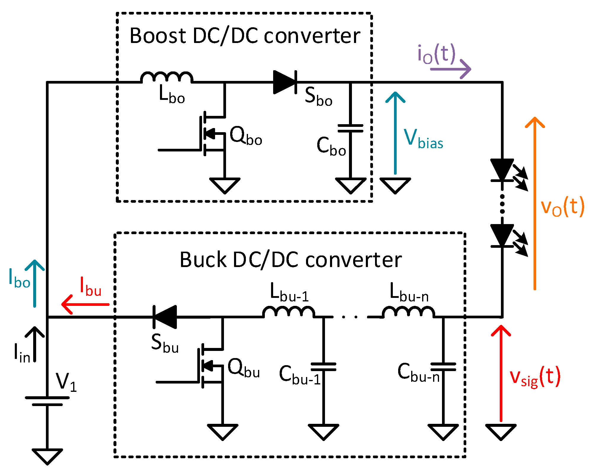
The block diagram of the proposed topology is shown in Figure 2a and an example for the waveforms are shown in Figure 2b. Both converters are connected to the same input voltage V1 and their outputs are connected in series with respect to the HB-LED string load. The HB-LED string load is comprised of n HB-LEDs. The Boost DC/DC converter is responsible for generating a DC voltage Vbias, while the Buck DC/DC converter generates the communication signal vsig(t), as shown in the block diagram in Figure 2(a).
In order to make the n HB-LED string work within the linear region (Figure 1), the HB-LED voltage vo(t) has to be between the threshold voltage nVth(T) and the maximum voltage nVmax(T), where Vth(T) and Vmax(T) are the threshold and maximum voltage of a single HB-LED, and nVavg(T) is the voltage in the middle of the linear region of the HB-LED string. For the sake of simplicity, the HB-LED string working range is defined according to the middle point of the linear region nVavg(T ). It is important to highlight that dependency with temperature is noted as (T).
The useful voltage range of the HB-LED load for communication (i.e., the peak-to-peak maximum amplitude allowed for the communication signal due to its linearity) is nVΩ, defined as follows
where nVΩ has no dependency with temperature. For the sake of simplicity, the limits of the useful voltage range of the HB-LED can be obtained from the middle point of the linear region, nVavg(T).
Considering (2) and (3), we can conclude that controlling nVavg(T) when temperature varies, always allows the HB-LED string to work at the middle point of the linear region that defines the useful voltage range of the HB-LED load for communication, nVΩ. From Figure 2(a) the expression of the voltage across the HB-LED string is
Vbias (voltage of the Boost DC/DC converter) only has a DC component (neglecting its ripple), while vsig(t) (voltage of the Buck DC/DC converter) can be represented by its average value (Vsig) plus the amplitude of the signal (Δvsig(t))
2.2. Resolution of the Buck DC/DC for Tracking the Output Voltage
The target is to keep the average voltage of the string of HB-LEDs Vo=avg(vo(t)) equal to nVavg(T) at any temperature. Moreover, it is important to note that Vo only depends on the average value of the output voltage of both converters, which is
Equation (6) shows that the biasing point can either be controlled by the average value of the Boost or the Buck DC/DC converters. If control of the temperature drift is implemented via the action of the Boost DC/DC converter, we can conclude that it is only the Boost DC/DC converter output voltage, Vbias, which compensates for temperature changes, making the average value of the Buck DC/DC converter independent of temperature. This is very important because the Buck DC/DC converter always has the maximum resolution in its duty cycle (i.e., dbu(t)) to track vo(t).
If dbu(t) is the duty cycle of the Buck DC/DC converter then vsig(t) can be expressed as a function of dbu(t) and V1
Substituting (7) in (4), the value of vo(t) becomes
with [0, 1] being the range of dbu(t); the highest output voltage occurs for dbu(t)=0 and the lowest output voltage occurs for dbu(t)=1. Considering previous definitions, the range of output voltage is [Vbias-V1, Vbias]. At this point, two design rules can be defined if we want the entire useful voltage range of the HB-LED load (i.e., nVΩ) to be used for communication
Figure 3(a) shows that the full range of dbu(t) defines useful voltages in the linear region of the HB-LED load, maximizing the resolution of the Buck DC/DC converter for tracking the output voltage for communication tasks.
Considering (1), (9) and (10) the following expression is obtained
Therefore, V1 determines the value of the voltage that maximizes the output voltage range of the Buck DC/DC to track it, which only depends on nVΩ. As previously mentioned, nVΩ does not depend on temperature. This is extremely important because maximization of the output voltage range of the Buck DC/DC for tracking the communication signal vsig(t) is independent of temperature. Figure 3 shows the representation of the output voltage range of the Buck DC/DC converter (by means of the dbu(t) useful range) versus the useful voltage range of the HB-LED load and their impact on the resolution when temperature changes from T2 to T1, with T1>T2. If (9) and (10) are fulfilled by the Boost DC/DC converter, two conclusions can be drawn. First, the Boost DC/DC converter is responsible for temperature changes. Second, the Boost DC/DC converter provides the maximum resolution to the Buck DC/DC converter for tracking its output voltage (i.e., vsig(t)) and therefore, the output voltage across the HB-LED load (i.e., vo(t)) versus temperature changes. Thus, the Series/Parallel Boost/Buck DC/DC Converter improves on the performance reported in [14] and [15] because it uses only a single input voltage source (unlike [14], which uses two). Moreover, the proposed converter is better than [15] in terms of resolution versus temperature changes. However, both converters process all power and the main switches are rated to the input voltage. This is the price to pay to use only one voltage source and the improvement in terms of resolution temperature changes .
2.3. Controlling the Average Value of the Voltage Across the HB-LERD Load
As previously mentioned, the Boost converter is responsible for controlling the average value of vo(t). With Dbias being the duty cycle of the Boost DC/DC converter, Vbias can be expressed as
By substituting (12) in (6), and assuming that the duty cycle of the buck converter is 0.5 to maximize useful dbu(t) range, the average value of output voltage can be rewritten as
3. Power Flow and Efficiency Analysis
An important consideration to study is the power flow between the two converters to achieve the power balance and efficiency of the Series/Parallel Boost/Buck DC/DC Converter. Note that the Boost DC/DC converter injects power to the HB_LED load, but the Buck DC/DC converter drains power from the HB_LED load.
3.1. Power Flow Analisys
As Figure 2(a) shows, Ibo is demanded by the Boost DC/DC converter from the voltage source V1. In contrast, the Buck DC/DC converter injects Ibu to V1. Therefore, Iin can be written as
The Boost converter injects an average power to the HB-LED load, generating the voltage Vbias and the Io current. In this case the power of the Boost DC/DC converter is
One part of the power is processed by the HB-.LED load, PLED. By using (4), PLED can be expressed as
where Vo is the average value of vo(t) and Vsig is the average value of vsig(t). The other part of the power is processed by the Buck DC/DC and drained from HB-LED load by injecting Ibu to V1. Thus, the Buck DC_/DC converter drains Pbu-in, which can be written as
3.2. Simplification of Series/Parallel Boost/Buck DC/DC
This converter’s way processing power allows it to be simplified. A Buck DC/DC converter that drains rather than supplies current can be analysed as a Boost DC/DC converter. Due to this, one possible Series/Parallel Boost/Buck DC/DC Converter implementation is that shown in Figure 5.
If the switching of both converters is asynchronous, it is possible to connect both MOSFET to ground, making implementation easier because an isolator is not needed to control the floating MOSFET in the Buck DC/DC converter.
Figure 4.
Representation of the simplification of the Series/Parallel Boost/Buck DC/DC Converter, where the switching of the two converters is asynchronous. This allows the control signals of both MOSFETs to be linked to ground.
Figure 4.
Representation of the simplification of the Series/Parallel Boost/Buck DC/DC Converter, where the switching of the two converters is asynchronous. This allows the control signals of both MOSFETs to be linked to ground.
3.3. Efficiency Analysis
Efficiency analysis is done by examining the efficiency of each converter in the Series/Parallel Boost/Buck DC/DC Converter. Figure 2(a) defines the efficiency of the Boost DC/DC converter as ηbo-lf and the efficiency of the Buck DC/DC converter as ηbu-hf. Moreover Figure 2(a) defines the input power as
The output power is defined in (16). Thus, the efficiency of the Series/Parallel Boost/Buck DC/DC Converter (i.e., ηt) can be easily defined by the output power divided by the input power
The input power of the Boost DC/DC converter can be expressed as a function of the input voltage and the input current
The output power of the Buck DC/DC converter can be expressed as a function of the input voltage and its output current.
By substituting (15), (17), (20) and (21) in (19), the efficiency ηt can be rewritten as
Input power of the Boost DC/DC converter (i.e., Pbo-in) can be rewritten as a function of its output power and its efficiency (i.e., ηbo-lf)
Following the same procedure the output power of the Buck DC/DC converter can be expressed as a function of its input power (i.e., Pbu-in) and its efficiency (i.e., ηbu-hf)
Taking into account (23) and (24), (22) can be rewritten as
In order to simplify the analysis of (25), a new parameter will be defined. This parameter is α, defined as
where α depends on the amplitude of the communication signal (i.e., Vsig) and the output voltage of the Boost DC/DC converter that defines the bias of the HB-LED load (i.e., Vbias)
Now, putting (26) into (25), the overall efficiency of the Series/Parallel Boost/Buck DC/DC Converter is
(27) shows the dependency of ηt on the efficiency of each converter in the Series/Parallel Boost/Buck DC/DC Converter architecture. For example, an edge case: When there is no signal, Vsig equals zero and therefore the overall efficiency is the efficiency of the Boost DC/DC converter.
It is important to note that the Series/Parallel Boost/Buck DC/DC Converter supplies an HB-LED load for communication. As explained in section 2.2, the idea is to take advantage of all useful voltages in the linear region of the HB-LED load. This means that Vsig value mut be 0.5VΩ. By using (7), (9), (11) and (26), the α parameter can be expressed as a function of the HB-LED characteristics
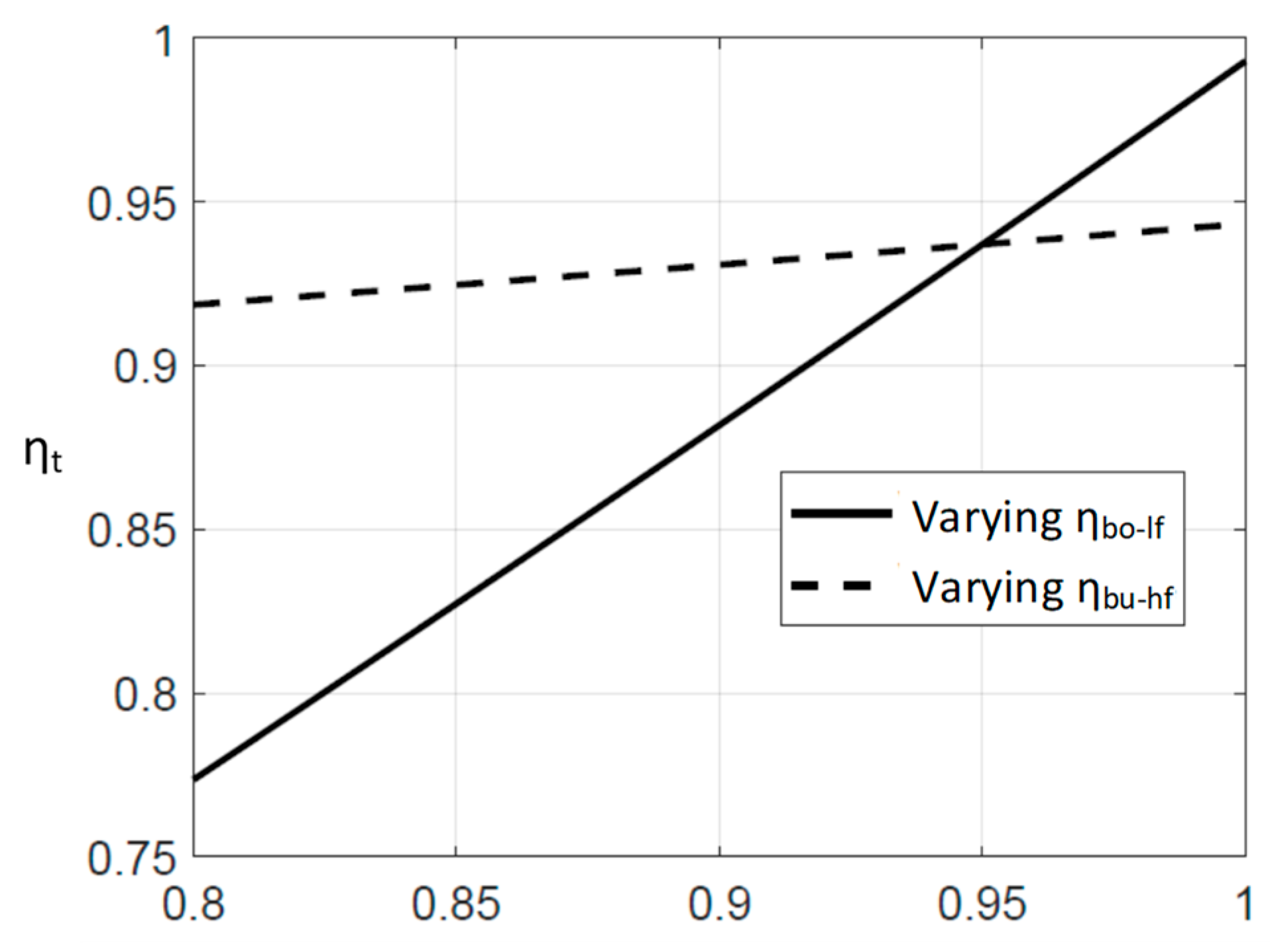
Taking typical values of commercial HB-LEDs [16], VΩ=1 and Vmax=4. These values define an α parameter of 0.125. Taking advantage of this calculation, it is very interesting to evaluate how each converter’s efficiency (i.e., Buck DC/DC converter and Boost DC/DC converter) influences the overall efficiency of the Series/Parallel Boost/Buck DC/DC converter. Figure 5, makes this analysis, evaluating ηt in two cases. First, keeping the efficiency of the Boost converter constant at 0.95 (i.e., ηbo-lf=0.5) and varying the efficiency of the Buck DC/DC converter between 0.8 and 1 (solid line in Figure 5). Second, keeping the efficiency of the Buck DC/DC converter constant at 0.95 and varying the efficiency of the Boost DC/DC converter between 0.8 and 1 (dotted line in Figure 5). As Figure 5 shows, the range of variation of ηt is lower when the efficiency of the Buck DC/DC converter varies and the efficiency of the Boost DC/DC converter is kept constant. It is clear that the efficiency of the proposed Series/Parallel Boost/Buck DC/DC converter depends more on the efficiency of the Boost DC/DC converter (i.e., ηbo-lf). This is because the Boost DC_/DC converter processes higher power levels, making its efficiency much more important. This is a notable benefit because the Boost DC/DC converter operates at a lower switching frequency and it is easier to achieve higher efficiency here than in the Buck DC/DC converter, which operates at a higher frequency.
Figure 5.
Effect of varying the efficiency of each individual DC/DC converter in ηt.
4. Experimental Results
To provide experimental results, the proposed VLC HB-LED driver was built. The proposed converter is based on a low frequency Boost DC/DC converter and a high frequency Buck DC/DC converter sharing the same input voltage and connected in series in relation to the HB-LED load (Figure 6).
The HB-LED load is a string of 8 XLamp MX-3 HB-LEDs, with an output power around 8 W. The current and voltage necessary for the HB-load can be obtained from the datasheet of the XLamp MX- 3 LED used [16]. A string of 8 XLamp MX-3 HB-LEDs has a maximum voltage of 32 V (4 V for a single LED) and a current of 0.25 A in the middle of the linear region. The working range is nVΩ= 8 V (1 V for a single LED). The input voltage used was V1 = n nVΩ = 8 V. As previously explained, this value of input voltage maximizes the resolution for tracking the output voltage for communication tasks.
The average current through the HB-LEDs was kept at 0.25 A (in the middle of the linear region) and the overall efficiency achieved was 91.5%. Efficiency was measured by comparing the DC input power to the RMS output power (taking into account biasing and communication power) on the HB-LED load.
A Field Programmable Gate Array (FPGA) (Nexys A7) was used both to control the Buck DC/DC converter and the Boost DC/DC converter using a Digital Pulse Width Modulator (DPWM). The FPGA controls the Boost DC/DC converter in order to control the average value of the current through the HB-LED load (i.e., controlling Vbias value using a control loop). The FPGA also controls the Buck DC/DC converter operating at high frequency in order to send information (i.e., reproducing the input bits at its output).
4.1. Effiuciency Analysis
The low frequency boost DC/DC converter is designed to work as a traditional HB- LED driver with a switching frequency of 100 kHz, working in a closed loop. It is responsible for increasing the dc output voltage up to the maximum voltage allowed across the LED. It also implements the bias current loop control of the LED string. Due to the low dynamic behaviour of the temperature shift in the LEDs, there is no need for the converter to have a fast output dynamic response. There needs to be a trade-off with regard to the switching frequency: increasing the switching frequency allows the reactive elements of the converter to be reduced (especially interesting in small applications), but it increases power losses and the effect of switching noise on communication (if this noise is within the communication band). The noise is produced by the output voltage ripple on the output boost capacitor Cbo. Using (10), the boost output ripple is limited to a maximum of 2% of the output boost voltage. The final values of the reactive elements of this converter are shown in Table 1.
In this equation, ΔQ is the total charge of the capacitor and Dbo and Tbo are the duty cycle and the time period of the boost DC/DC converter. A current control was implemented so that the boost DC/DC converter could control the Io current. The current was measured by means of an isolated current shunt, connected in series to the LED string. The current control included a low pass filter which eliminates the communication components in the HB-LED current and a PI controller. No new considerations are needed with regard to the PI controller in this implementation, and a standard current controller for HB-LED can be used. Both the PWM modulation and the current control were implemented in a FPGA Nexys A7, as noted previously. The remaining component selection was as follows: the dual CSD88539 MOSFET was used for Q1bo and Q2bo; an ISL6700 half bridge driver was used for the driving stage. The complete list of components are summarized in Table 2.
4.2. Effiuciency Analysis
The converter reproduces a 64-QAM modulation, with a carrier frequency fsig of 1 MHz. The symbol period is equal to four signal periods, achieving a maximum bit rate of 1.5 Mbps. In order to avoid any switching noise coming from the Boost DC/DC converter, the signal frequency was selected a decade higher than the Boost DC/DC converter switching frequency.
4.3. High Frequency and Fast Response Buck DC/DC Converter Design
The high frequency Buck DC/DC converter is responsible for generating the communication signal as mentioned previously. This converter works in an open loop and includes a high order output filter to achieve high bandwidth and a fast response. To properly reproduce a communication signal by means of a Buck DC/DC converter, the inequation
relating to the carrier frequency fsig, the cut-off frequency of the filter fcut, and the Buck DC/DC converter switching frequency fbu, must be applied. The exact relation between the frequencies and the order and attenuation of the filter was analysed in [17]. Based on this analysis, the output filter used a 6th low-pass filter with a cutoff frequency fcut of 2.5 MHz. The reactive components of the filter are shown in Table 2. The switching frequency fbu used was 10 MHz
Due to the high switching frequency of the Buck DC/DC converter, two RF high frequency PD84010-E MOSFETs were used for Q1bu and Q2bu in parallel with two high speed Schottky UPS115UE3 diodes. For the driving stage two high speed EL7155CSZ drivers were used.
4.4. Experimental Results for Communication
Figure 7 shows some of the most representative waveforms of the DC/DC converters. The signals vgs-bot and vgs-bu are the gate-to-source signals of the Boost and Buck DC/DC converters respectively. The difference in frequency between these two signals is notable, vgs-bot is a 100 kHz PWM signal, while vgs-bu is a 10 MHz PWM signal. The signals Vbias and vsig(t) are the output voltage of the Boost and Buck DC/DC converters respectively. As shown, the output voltage of the Boost DC/DC converter is kept constant (and with low ripple) and the current loop control varies the duty cycle of the signal vgs-bot in order to keep the average output current constant through the HB-LEDs, at the design level of 0.25 A. Without considering any temperature shift over the HB-LED, the input voltage of the Boost DC/DC converter should be 32 V, which is the maximum HB-LED voltage of the 8 LED string used. After a few minutes, when the LED temperature is stabilized, the current control loop of the boost dc-dc converter reduces Vbias by 21% to 25 V.
The Buck DC/DC converter works in an open loop reproducing the communication signal. The variation of the duty cycle in vgs-bu can be seen, along with the effect over the output voltage vo(t). The peak to peak voltage of the Buck DC/DC converter is 7.5 V, closer to the maximum working range of the 8 HB-LED string, which is 8 V. The output Buck DC/DC converter filter is able to filter the high switching frequency of the converter and allows the communication signal to pass through. The correct design of this filter must take into account the correct reproduction of the sine carrier frequency of the modulation and the correct change in phase and amplitude between symbols.
In order to focus the analysis on the converter’s communication task, a longer period of time is shown in Figure 8. Thus to test the communication performance, the communication signal generated by the Buck DC/DC converter vsig(t) and the light emitted by the HB-LEDs were measured during transmission of 12 different symbols. To properly measure the light, a Thorlabs PDA10A-EC [18] high bandwidth optical receiver was used, placed in front of the HB-LED string, giving an output voltage vrx(t) proportional to the light. Comparing the two signals vo(t) and vrx(t) shows that the converter was able to properly reproduce the communication signal without distortion. Distortion could occur due to temperature shifts in the HB-LEDs by making the HB_LED work outside its linear region. Comparing the vo(t) and its received light signal vrx(t) indicates that this undesired effect was avoided due to proper current loop control.
In terms of efficiency, the experimental results were gathered using 34461A Digital Multimeterers and indicated an efficiency of 91.5% reproducing a 64-QAM digital modulation, with a bit rate of 1.5 Mbps
5. Conclusions
The proposed HB-LED driver for VLC can achieve high efficiency and high communication performance by means of splitting the power between two different converters. The design is based on two converters connected to the same input voltage, with their outputs connected in series in relation to the HB-LED load. A low frequency Boost DC/DC converter working in a closed loop is responsible for delivering most of the power and controlling the bias of the HB-LEDs. In contrast, an open loop, fast response Buck DC/DC converter is responsible for generating the communication signal. Advantages of this approach include high efficiency, high communication capability, input voltage flexibility, and improved duty resolution. The overall power efficiency is improved by means of splitting the power between two converters where the communication signal is delivered by the high frequency converter and the bias power is processed by the low frequency boost. Another advantage is the flexibility in terms of input voltage. In contrast to other topologies based only on buck converters, the input voltage can be lower than the threshold voltage of the LED string. An additional effect of lower input voltages is increased resolution of the duty cycle for tracking the output voltage in the high frequency Buck DC/DC converter. The experimental results demonstrated an efficiency of 91.5% reproducing a 64-QAM digital modulation, with a bit rate of 1.5 Mbps.
Author Contributions
D.G.A. and J.R. conceived and performed the experiments. D.G.A. and J.S. developed the adaptation of solutions to VLC and the design procedure. D.G.L. and D.G.A. analysed the data and wrote the paper. MMH., J.R.G. M. and J.S. contributed to the definition, the design, and the evaluation of the experiments and the revision of the paper. All authors have read and agreed to the published version of the manuscript.
Funding
This work was funded by the Principality of Asturias under the proyect GRU-GIC-24-036, the “Severo Ochoa” Program and the project Grant no. BP20-181 and by the FEDER funding.
References
- Cisco Systems. Cisco Annual Internet Report - Cisco Annual Internet Report (2018–2023) White Paper. URL: (visited on 2024-11-09).
- “IEEE Standard for Local and metropolitan area net-works–Part 15.7: Short-Range Optical Wireless Communications”. In: IEEE Std 802.15.7-2018 (Revision of IEEE Std 802.15.7-2011) (Apr. 2019). Conference Name: IEEE Std 802.15.7-2018 (Revision of IEEE Std 802.15.7-2011), pp. 1–407. [CrossRef]
- Luiz Eduardo Mendes Matheus, Alex Borges Vieira, Luiz F. M. Vieira, et al. “Visible Light Communication: Concepts, Applications and Challenges”. In: IEEE Communications Surveys Tutorials 21.4 (2019). Conference Name: IEEE Communications Surveys Tu-torials, pp. 3204–3237. ISSN: 1553-877X. [CrossRef]
- Saeed Ur Rehman, Shakir Ullah, Peter Han Joo Chong, et al. “Visible Light Communication: A System Per-spective—Overview and Challenges”. en. In: Sensors 19.5 (Jan. 2019). Number: 5 Publisher: Multidisci-plinary Digital Publishing Institute, p. 1153. [CrossRef]
- Dilukshan Karunatilaka, Fahad Zafar, Vineetha Kalavally, et al. “LED Based Indoor Visible Light Communications: State of the Art”. In: IEEE Communications Surveys Tutorials 17.3 (2015). Conference Name: IEEE Communications Surveys Tutorials, pp. 1649–1678. ISSN: 1553-877X. [CrossRef]
- Raed Mesleh, Hany Elgala, and Thomas D. C. Little. “On the performance degradation of optical wireless OFDM communication systems due to changes in the LED junction temperature”. In: ICT 2013. May 2013, pp. 1–5. [CrossRef]
- A. M. Khalid, G. Cossu, R. Corsini, et al. “1-Gb/s Transmission Over a Phosphorescent White LED by Using Rate-Adaptive Discrete Multitone Modulation”. In: IEEE Photonics Journal 4.5 (Oct. 2012). Confer-ence Name: IEEE Photonics Journal, pp. 1465–1473. ISSN: 1943-0655. [CrossRef]
- Xingxing Huang, Jianyang Shi, Jiehui Li, et al. “A Gb/s VLC Transmission Using Hardware Preequalization Circuit”. In: IEEE Photonics Technology Letters 27.18 (Sept. 2015). Conference Name: IEEE Photonics Technology Letters, pp. 1915–1918. ISSN: 1941-0174. [CrossRef]
- Hyunchae Chun, Sujan Rajbhandari, Grahame Faulkner, et al. “LED Based Wavelength Division Multiplexed 10 Gb/s Visible Light Communications”. In: Journal of Lightwave Technology 34.13 (July 2016). Conference Name: Journal of Lightwave Technology, pp. 3047–3052. ISSN: 1558-2213. [CrossRef]
- Marian K. Kazimierczuk. RF Power Amplifiers. en. John Wiley & Sons, Ltd, 2014. ISBN: 978-1-118-84437-3.
- Rodríguez, J.; Lamar, D.G.; Aller, D.G.; Miaja, P.F.; Sebastián, J. Efficient Visible Light Communication Transmitters Based on Switching-Mode dc-dc Converters. Sensors 2018, 18, 1127. [CrossRef]
- Felipe Loose, Lucas Teixeira, Renan R. Duarte, et al. “On the Use of the Intrinsic Ripple of a Buck Converter for Visible Light Communication in LED Drivers”. In: IEEE Journal of Emerging and Selected Topics in Power Electronics 6.3 (Sept. 2018). Conference Name: IEEE Journal of Emerging and Selected Topics in Power Electronics, pp. 1235–1245. ISSN: 2168-6785. [CrossRef]
- Javier Sebastian, Diego G. Lamar, Daniel G. Aller, et al. “On the Role of Power Electronics in Visible Light Communication”. In: IEEE Journal of Emerging and Selected Topics in Power Electronics 6.3 (Sept. 2018). Conference Name: IEEE Journal of Emerging and Selected Topics in Power Electronics, pp. 1210–1223. ISSN: 2168-6785. [CrossRef]
- Juan Rodriguez, Diego G. Lamar, Pablo F. Miaja, et al. “Power-Efficient VLC Transmitter Based on Pulse-Width Modulated DC–DC Converters and the Split of the Power”. In: IEEE Transactions on Power Electronics 34.2 (Feb. 2019). Conference Name: IEEE Transactions on Power Electronics, pp. 1726–1743. ISSN: 1941-0107. [CrossRef]
- Aller, D.G.; Lamar, D.G.; García-Mere, J.R.; Arias, M.; Rodriguez, J.; Sebastian, J. Performance Evaluation of the Two-Input Buck Converter as a Visible Light Communication High-Brightness LED Driver Based on Split Power. Sensors 2024, 24, 6392. [CrossRef]
- Cree Components. XLamp MX-3 LEDs—Cree Com-ponents. URL: https://www.cree-led.com/products/leds/xlamp/ (visited on 2024-11-07).
- Javier Sebastian, Pablo Fernandez-Miaja, Alberto Rodriguez, et al. “Analysis and Design of the Output Filter for Buck Envelope Amplifiers”. In: IEEE Trans-actions on Power Electronics 29.1 (Jan. 2014). Confer-ence Name: IEEE Transactions on Power Electronics, pp. 213–233. ISSN: 1941-0107. [CrossRef]
- Thorlabs. PDA10A-EC Si Fixed Gain Detector, 200-100 nm, 150 MHz BW. URL: https://www.thorlabs.com/thorproduct.cfm?partnumber=PDA10A-EC (visited on 2024-11-07).
- D. G. Aller, D. G. Lamar, M. Arias, P. F. Miaja and J. Sebastián, "Design of a high performance VLC-LED driver for Visible Light Communication based on the split of the power," 2020 IEEE 21st Workshop on Control and Modeling for Power Electronics (COMPEL), Aalborg, Denmark, 2020, pp. 1-8. [CrossRef]
Figure 1.
Temperature shift in HB-LED curves (string of n HB_LEDs).
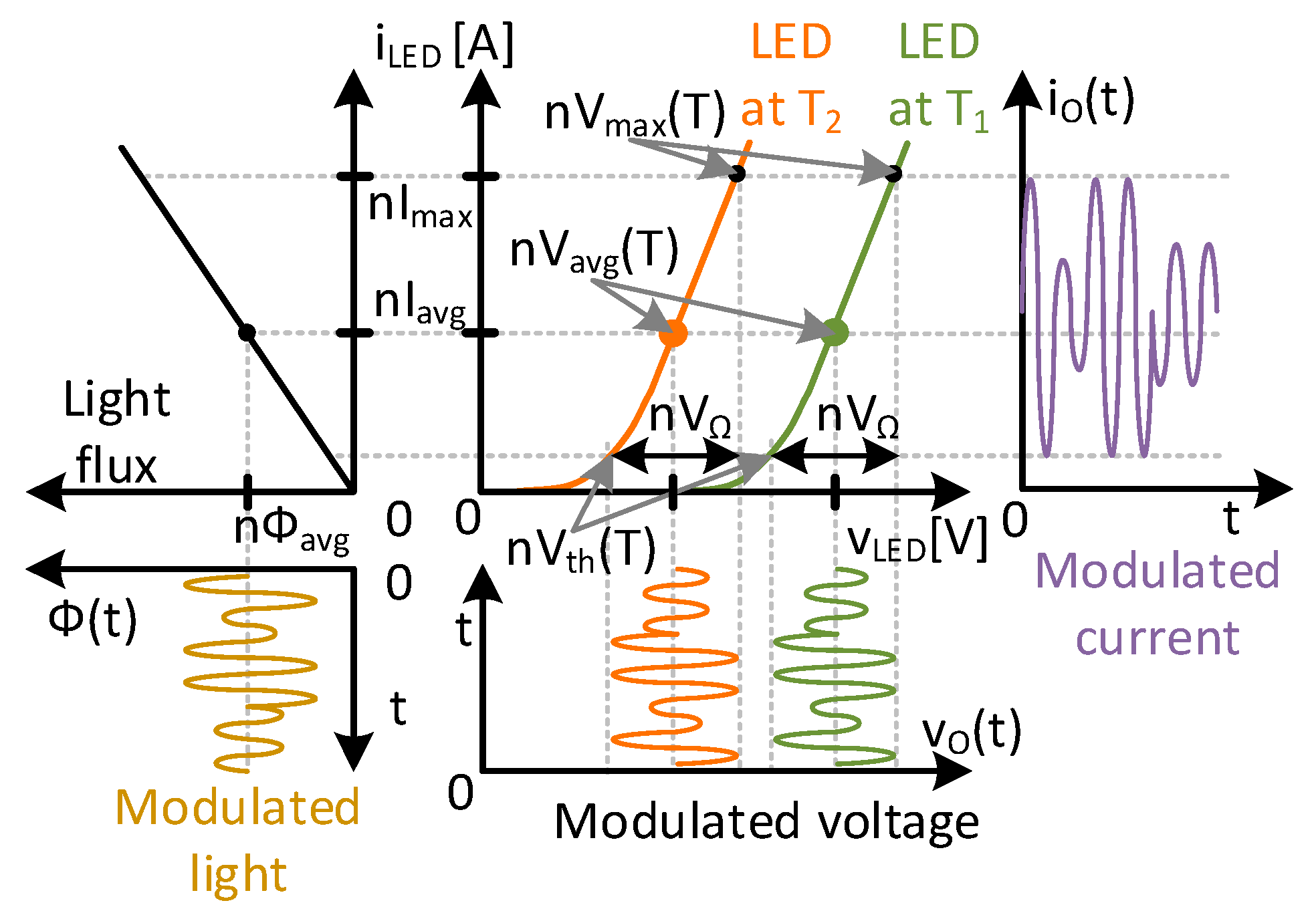
Figure 2.
(a) Block diagram of the proposed Series/Parallel Boost/Buck DC/DC converter acting as a VLC HB-LED driver. (b) Main waveforms of the proposed Series/Parallel Boost/Buck DC/DC converter acting as a VLC HB-LED driver.
Figure 2.
(a) Block diagram of the proposed Series/Parallel Boost/Buck DC/DC converter acting as a VLC HB-LED driver. (b) Main waveforms of the proposed Series/Parallel Boost/Buck DC/DC converter acting as a VLC HB-LED driver.
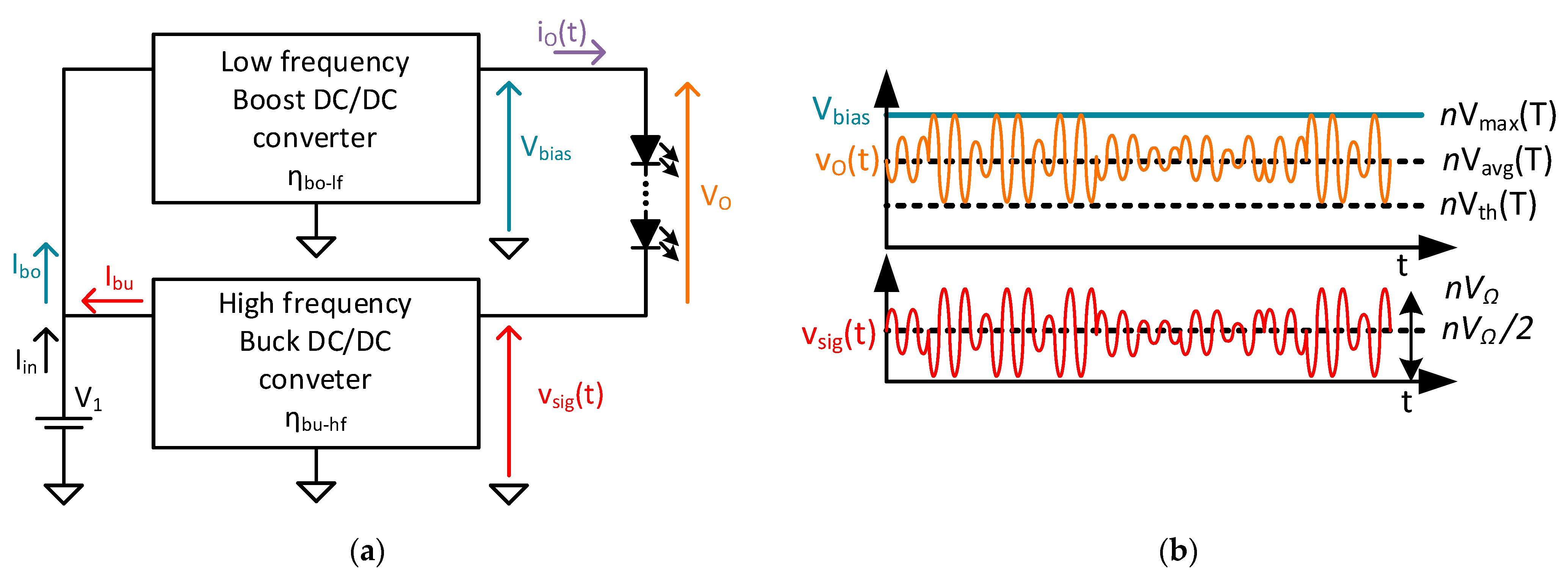
Figure 3.
Representation of the output voltage range of the Buck DC/DC converter versus the useful voltage range of the HB-LED load and their impact on resolution for tracking the output voltage. (a) Without temperature change. (b) With an increase of temperature.
Figure 3.
Representation of the output voltage range of the Buck DC/DC converter versus the useful voltage range of the HB-LED load and their impact on resolution for tracking the output voltage. (a) Without temperature change. (b) With an increase of temperature.
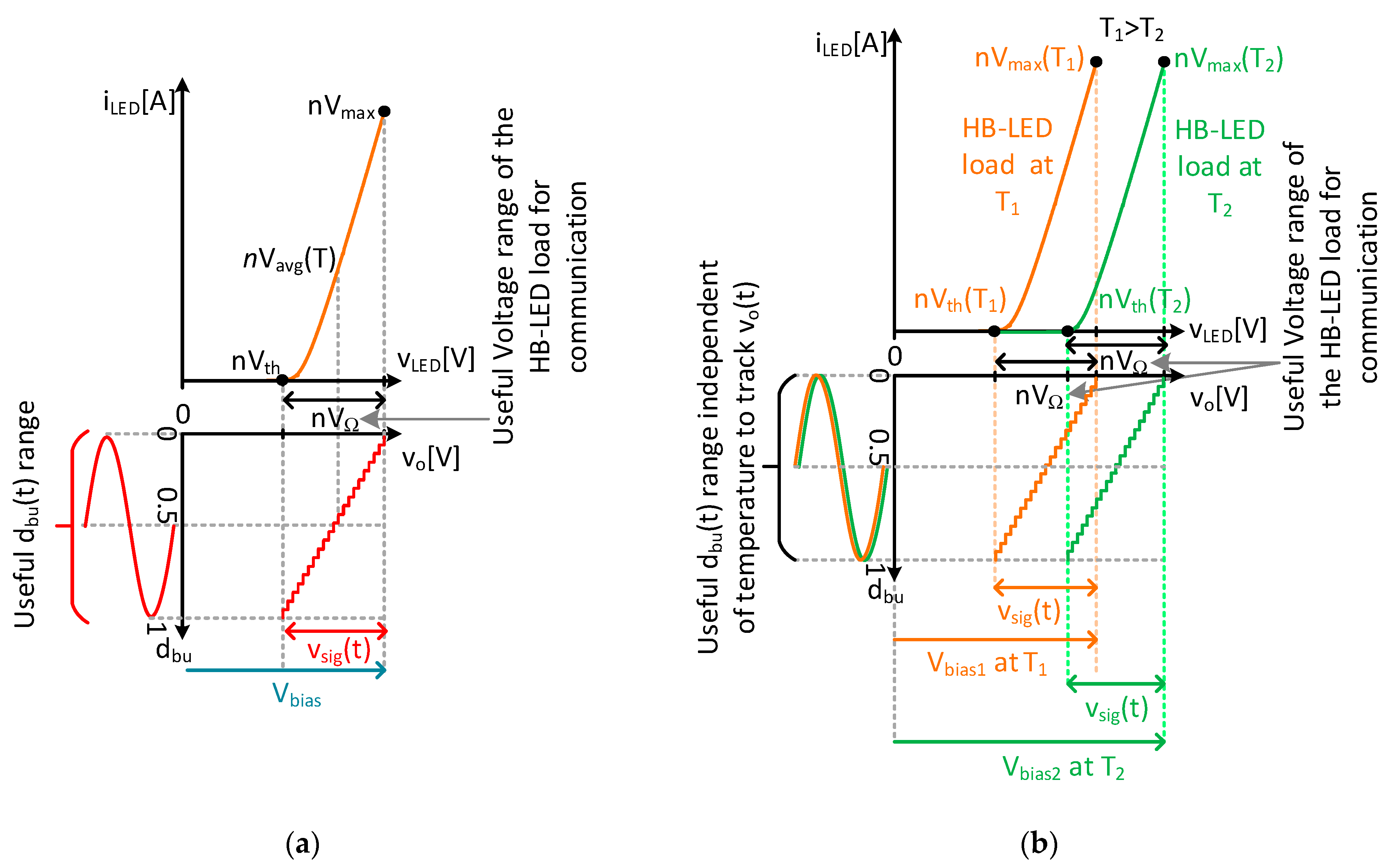
Figure 6.
(a) Schematic and control for the Series/Parallel Boost/Buck DC/DC Converter. (b) Photograph of the prototype.
Figure 6.
(a) Schematic and control for the Series/Parallel Boost/Buck DC/DC Converter. (b) Photograph of the prototype.
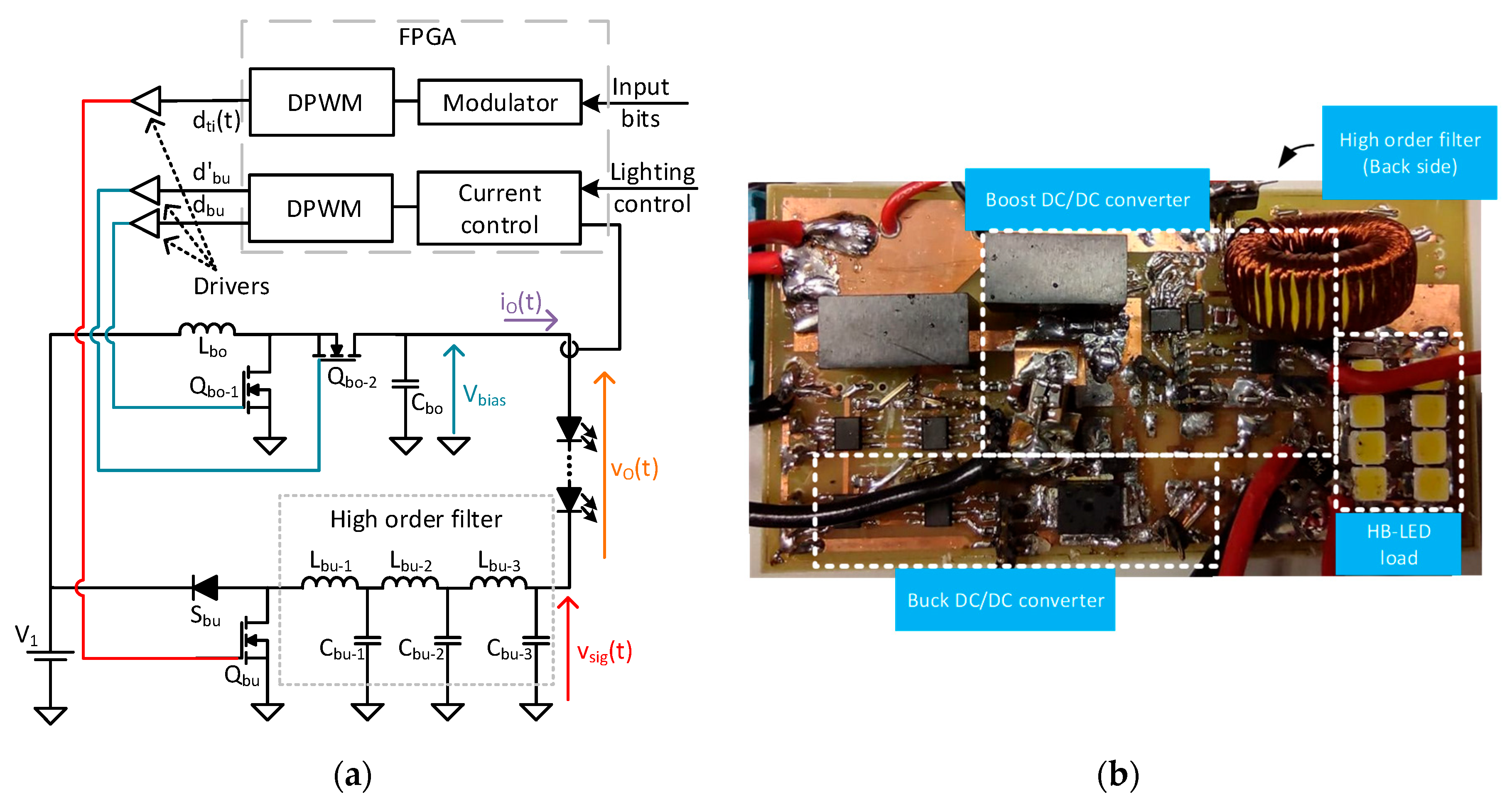
Figure 7.
Gate signal of the Buck and Boost DC/DC converters vgsbuck (orange) and vgsboost (blue), output voltage of the Boost DC/DC converter (green) and output voltage of the signal (magenta).
Figure 7.
Gate signal of the Buck and Boost DC/DC converters vgsbuck (orange) and vgsboost (blue), output voltage of the Boost DC/DC converter (green) and output voltage of the signal (magenta).
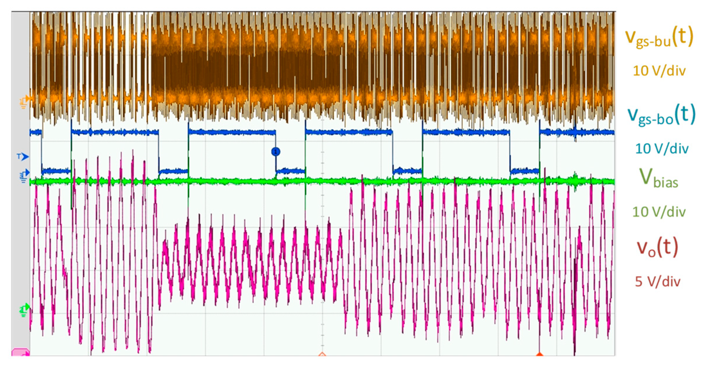
Figure 8.
Gate signals of the Buck and Boost DC/DC converters vgs-bu and vgs-bo, output voltage of the buck converter vo(t) and the voltage of the optical receiver vrx during a transmission.
Figure 8.
Gate signals of the Buck and Boost DC/DC converters vgs-bu and vgs-bo, output voltage of the buck converter vo(t) and the voltage of the optical receiver vrx during a transmission.
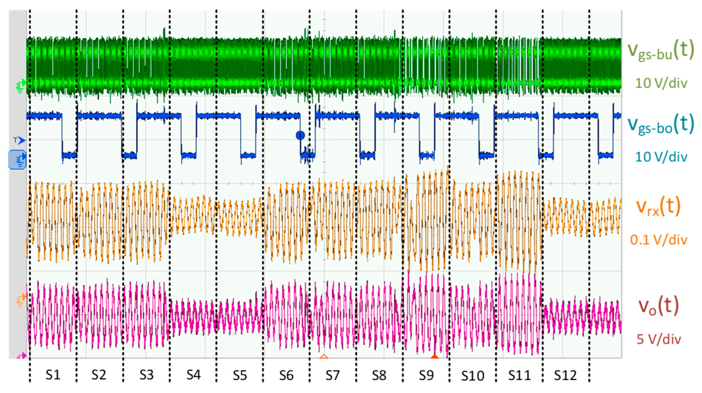

Table 1.
Circuit components of the VLC HB-LED driver.
| Q1bo and Q2bo | Boost driver | Lbo | Cbo | Q1bu and Q2bu | D1bu and D2bu | Buck drivers | HB-LEDs |
| CSD88539 | ISL6700 | 71 µH | 9 µF | PD84010-E | UPS115UE3 | EL7155CSZ | XLamp MX-3 |
Table 2.
Circuit components of the VLC HB-LED driver.
| Lbu1 | Cbu1 | Lbu2 | Cbu2 | Lbu3 | Cbu3 |
| 1.7µH | 9.9nF | 2.2µH | 9.9nF | 1.9µH | 5.72nF |
Disclaimer/Publisher’s Note: The statements, opinions and data contained in all publications are solely those of the individual author(s) and contributor(s) and not of MDPI and/or the editor(s). MDPI and/or the editor(s) disclaim responsibility for any injury to people or property resulting from any ideas, methods, instructions or products referred to in the content. |
© 2025 by the authors. Licensee MDPI, Basel, Switzerland. This article is an open access article distributed under the terms and conditions of the Creative Commons Attribution (CC BY) license (http://creativecommons.org/licenses/by/4.0/).
Copyright: This open access article is published under a Creative Commons CC BY 4.0 license, which permit the free download, distribution, and reuse, provided that the author and preprint are cited in any reuse.


