Preprint
Article

This version is not peer-reviewed.

Microfluidic Gel Chromatography-Enabled In-Situ Raman Spectroscopy for Selective Electronic-Type Separation and Analysis of Single-Walled Carbon Nanotubes

A peer-reviewed article of this preprint also exists.

Submitted:

03 December 2024

Posted:

04 December 2024

You are already at the latest version

Abstract

Single-walled carbon nanotubes (SWNTs) possess unique electronic properties—either metallic or semiconducting—defined by their chirality, making their selective separation a cornerstone for advancing nanotechnology applications. While conventional gel chromatography has proven effective for large-scale separation, the demand for microscale precision to uncover nanoscale interaction mechanisms and optimize separation strategies remains unmet. In this study, we report the development of a polydimethylsiloxane (PDMS)-based microfluidic platform integrating gel chromatography with in-situ Raman spectroscopy to achieve high-resolution electronic-type separation of SWNTs. By systematically isolating metallic- and semiconducting-enriched fractions (M1-M3, S1-S3), our approach leverages real-time Raman spectroscopy to reveal dynamic shifts in G-band characteristics and G⁻/G⁺ intensity ratios, providing quantitative insights into separation efficiency and purity. The platform’s novel integration of rate constant analysis and SDS concentration normalization highlights the inherent elution kinetics of SWNTs, with metallic SWNTs exhibiting accelerated separation dynamics compared to their semiconducting counterparts. This advancement not only enhances the resolution of electronic-type differentiation but also underscores the critical role of dispersant concentration in fine-tuning separation outcomes. The results establish this PDMS microchannel system as a versatile and scalable solution, bridging the gap between industrial-scale separations and microscale precision, paving the way for cutting-edge nanomaterial purification technologies.

Keywords: 
;  ;  ;  ;  

1. Introduction

Carbon nanotubes (CNTs), remarkable carbon allotropes, are celebrated for their unique cylindrical structure formed by rolling a single graphene sheet into a seamless tubular configuration. Among these, single-walled carbon nanotubes (SWNTs) have garnered significant attention since their discovery by Iijima in 1991 [1]. The nanoscale diameter and structural precision of SWNTs endow them with extraordinary properties, including high electrical conductivity, tensile strength, and mechanical flexibility. These properties are intricately linked to their chirality, defined by the chiral indices (n, m), which determine their electronic nature. Depending on the chiral angle, SWNTs can exhibit either metallic or semiconducting behavior. Specifically, SWNTs with (nm) mod 3 = 0 are metallic, while other configurations display semiconducting characteristics [2,3]. This dichotomy in electronic properties underscores the need for precise separation of SWNTs, as their mixed synthesis often hinders their direct application in advanced electronic devices, such as transistors, sensors, and energy storage systems [4,5,6,7,8,9,10]. The bandgap in semiconducting SWNTs varies with chirality, underscoring the importance of precise separation methods that enable targeted use in electronic devices. However, achieving separation by chirality remains a significant technical hurdle, as the controlled growth of SWNTs with predefined electronic properties is not yet viable. Consequently, a range of separation methods—including gel chromatography, density gradient centrifugation, and electrophoresis—have been developed to address this issue, with gel chromatography emerging as a particularly promising method for large-scale, chirality-specific separation.
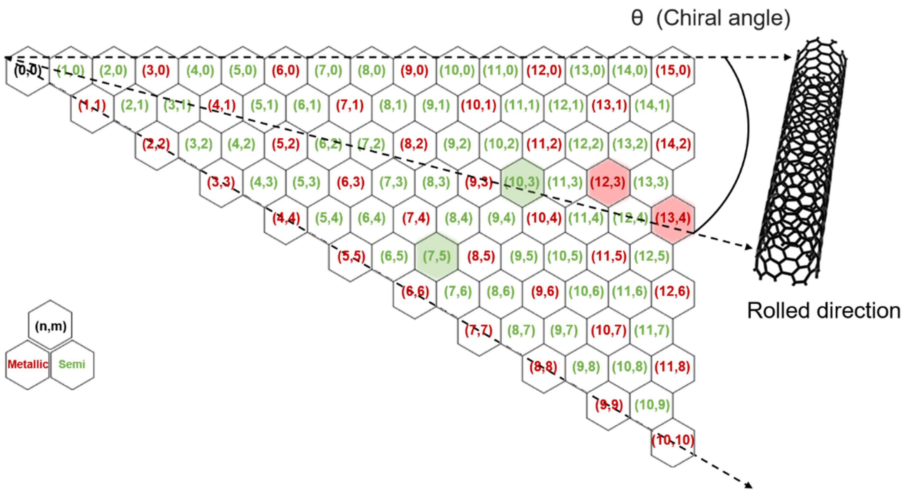
Figure 1. Map illustrating the structural and electronic characteristics of SWNTs based on their chirality. The hexagonal lattice defines the relationship between chiral indices (n, m), chiral angle (θ), and rolled direction, which collectively determine whether a given SWNT is metallic (red) or semiconducting (green). Four specific chiralities—(13,4), (12,3), (10,3), and (7,5)—are highlighted and correspond to distinct peaks in the Raman spectra shown in Figure 5. These chiralities are used to analyze the relative intensity ratios and provide insight into the selective separation of metallic- and semiconducting-enriched SWNTs.
Preprints 141654 g001
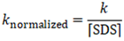
Gel chromatography is based on the adsorption and desorption of SWNTs with different affinities to the gel matrix, depending on their electrical properties. Agarose or dextran-based hydrogels used in gel chromatography exhibit varying affinities for SWNTs depending on their electrical characteristics, enabling selective adsorption of SWNTs with distinct properties [10,11]. Sodium dodecyl sulfate (SDS), a common dispersant for SWNTs, facilitates the desorption of nanotubes from the gel depending on its concentration and the degree of dispersion. This chemical adsorption and desorption mechanism, involving both the gel and dispersant, enables the selective separation of SWNTs with specific structures and electrical properties [12]. In particular, gel chromatography is a suitable method for separating metallic and semiconducting SWNTs, as these two types can be effectively segregated by adjusting the amount of SDS [13]. The ability to achieve separation through controlling concentrations of chemical agents makes gel chromatography advantageous for large-scale separation processes. However, despite its proven efficacy for large-scale applications, the detailed interaction mechanisms within the gel matrix remain poorly understood, posing challenges for optimization and extending its utility to microscale precision.
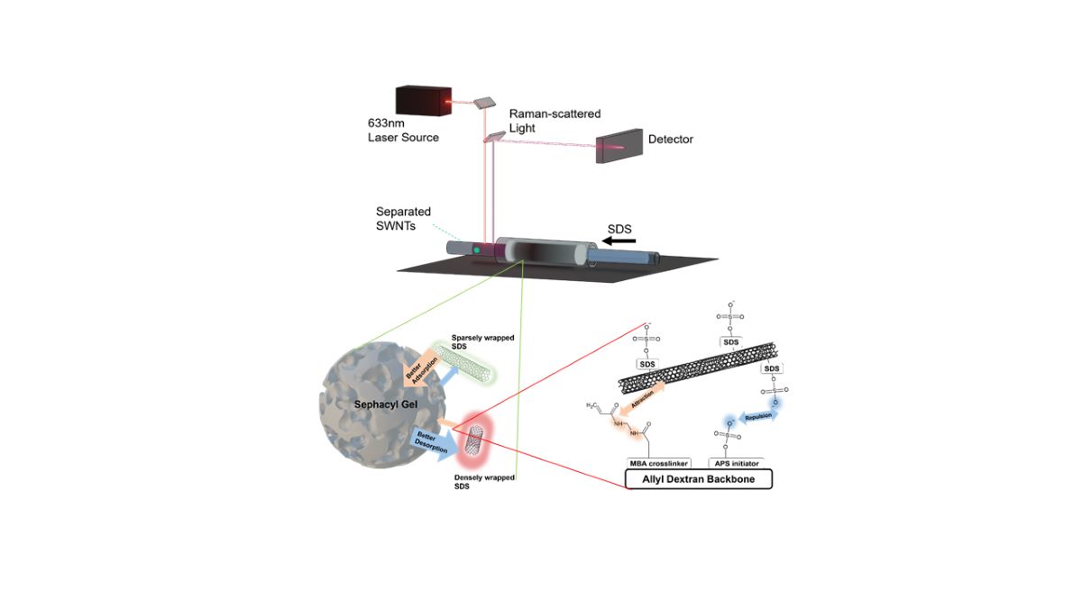
While much research has focused on large-scale separation techniques suitable for commercial production, small-scale methods are equally vital. Microscale separation provides an opportunity to observe SWNTs dynamics with greater precision, uncovering intricate molecular interactions and enabling real-time monitoring of separation processes. Additionally, micro-sized columns allow for both qualitative and quantitative analyses of SWNTs behavior via spectroscopic methods, which is invaluable for refining separation techniques and advancing toward scalable industrial applications. In the present study, we introduce a novel micro-sized polydimethylsiloxane (PDMS) column-based gel chromatography system designed to investigate the separation dynamics of SWNTs at a microscopic scale. PDMS, known for its transparency and ease of patterning, is an ideal material for constructing microfluidic channels that simulate the chromatographic environment [14,15]. This study pioneers the integration of gel chromatography within PDMS-based microfluidic channels, combining the precision of microscale separation with real-time, in-situ Raman spectroscopic analysis. This approach not only facilitates the isolation of metallic and semiconducting SWNTs but also reveals their elution kinetics and purity with unprecedented clarity. By systematically isolating and analyzing SWNT fractions, this work provides a comprehensive framework for understanding the interplay between SDS concentration, flow dynamics, and electronic-type separation. Furthermore, the integration of in-situ Raman spectroscopy allows for dynamic tracking of G-band characteristics and G-/G+ intensity ratios, offering quantitative insights into the separation process. This study demonstrates that metallic SWNTs exhibit accelerated separation dynamics compared to semiconducting SWNTs, a distinction further emphasized when normalized for SDS concentration. The results establish this PDMS-based platform as a versatile tool for both fundamental research and scalable industrial applications, bridging the gap between the demands of large-scale separations and the precision required for nanoscale studies.

2. Materials and Methods

2.1. Materials

In this study, Purified HiPco SWNTs (Nanointegris, HP34-093) were used for separation. Sodium dodecyl sulfate (SDS, ≥98.5%, Sigma-Aldrich, Cat. No. L3771) was used for dispersing the SWNTs. Disposable 10ml Polypropylene Columns (Thermo Fisher Scientific, Cat. No. 29924) were purchased and used along with polypropylene columns and polyethylene separators for SWNTs separation. Sephacryl™ S-200 HR gel (Cytiva) was used for separating the SWNTs. The PDMS mold was prepared using Sylgard184 (DOW CORNING) with the provided curing agent.

2.2. Dispersion of SWNTs

SWNTs were dispersed in 0.5wt% SDS at a concentration of 1mg/1ml. Tip sonication was used for 5 hours for dispersion. The dispersed SWNTs solution was then centrifuged at 32,000 rpm to remove impurities and metal catalysts remaining after synthesis. Only the top 20% supernatant of the solution was collected and used for separation.

2.3. Gel Chromatography

2.3.1. Conventional Column Method

The conventional column method for separating metallic and semiconducting SWNTs relies on differences in SDS wrapping behavior around the nanotubes. Metallic SWNTs, due to their unique electronic properties, are more effectively wrapped by SDS compared to semiconducting SWNTs, as illustrated in Figure 2a. This differential wrapping enhances their interaction with the Sephacryl gel, facilitating selective adsorption and subsequent desorption. Metallic SWNTs adsorbed onto the gel can be eluted with a lower SDS concentration, whereas higher concentrations are required for semiconducting SWNTs, which interact more strongly with the gel. The functional groups in the gel structure, as depicted in Figure 2b, play a pivotal role in this selective separation. The Sephacryl gel used in this study is a polymer gel constructed on an allyl dextran backbone chain. During the synthesis of the gel beads, ammonium persulfate (APS) acts as the initiator, and N,N′-methylenebisacrylamide (MBA) serves as the crosslinking agent. These components endow the gel with specific functional groups that are critical to its interaction with SWNTs. In the final synthesized gel, the organosulfate groups originating from APS and the amide groups derived from MBA facilitate interactions between the gel matrix and SWNTs. These functional groups play a critical role in enhancing the compatibility and interaction strength between the gel and the nanotubes, as previously reported [9,16].
The organosulfate groups are negatively charged and interact through electrostatic repulsion with the negatively charged sulfate groups of SDS. This repulsive force is particularly significant for SDS-wrapped SWNTs, whose degree of wrapping modulates their adsorption behavior on the gel. In contrast, the amide groups act as electron donors, creating attractive interactions with the SWNT surface [9]. These opposing forces create a selective adsorption mechanism based on the electronic properties of the SWNTs. Metallic SWNTs, which are typically more sparsely wrapped with SDS, exhibit weaker repulsion from the organosulfate groups, resulting in stronger interactions with the gel matrix. Conversely, semiconducting SWNTs, which are more densely wrapped with SDS, experience greater repulsion, reducing their affinity for the gel. Simultaneously, the degree to which SDS wraps the SWNTs directly influences their desorption behavior. As SDS concentration increases, the interaction between SDS-wrapped SWNTs and the gel is systematically modulated. This mechanism enables the sequential elution of metallic and semiconducting SWNTs through gradual changes in SDS concentration, as illustrated in Figure 2c. The selective interaction between the gel and SWNTs, driven by the balance of repulsive and attractive forces, highlights the efficacy of this system in separating SWNTs based on their electronic properties. [17,18].
Figure 2c outlines the experimental setup for gel chromatography. Ethanol-washed columns with membranes at the base are used to prevent gel leakage. A volume of 4 ml of Sephacryl gel is loaded into the column, followed by the injection of 1 ml of an unseparated SWNT solution. The SWNTs adsorbed onto the gel are eluted sequentially. Metallic SWNTs are first eluted using 1 ml of 0.5 wt% SDS, while semiconducting SWNTs are eluted with 1 ml of 5 wt% SDS following a cleaning step using 5 ml of 0.5 wt% SDS. This stepwise elution process ensures a high degree of separation, with the SDS concentration precisely tuned to exploit the differences in SWNT-gel interactions.

2.3.2. Microchannel Column Method

To fabricate the microchannel system, polydimethylsiloxane (PDMS) was mixed with a curing agent and poured into a mold containing a wire template with a radius of 800 μm. The mixture was degassed under vacuum and subsequently cured at 90°C for 1 hour to achieve crosslinking. Once the curing was complete, the wire was carefully removed, leaving behind a cylindrical microchannel with a radius of 800 μm. As illustrated in Figure 3, the microchannel mold was thoroughly washed with ethanol to remove any residual contaminants. The PE membrane was then placed within the channel, replicating the gel retention setup used in conventional column chromatography. The Sephacryl gel was loaded into the channel, and Teflon tubes were attached to the inlet and outlet of the microchannel to connect it to an external syringe pump. To test the adsorption capability of the gel within the microchannel, a dispersed SWNT solution was injected. Using a syringe pump to simulate the gravitational force in traditional chromatography, SDS solutions of 0.5 wt% and 5 wt% were sequentially introduced to achieve selective elution of metallic and semiconducting SWNTs, respectively. This setup provided a refined and precise means of SWNT separation within a controlled microfluidic environment.
After mixing PDMS with a curing agent, a wire with a radius of 800 μm was positioned to create the microchannel. The mixture was degassed using a vacuum desiccator, and crosslinking was conducted by heating at 90°C for 1 hour. The wire inside the mold was subsequently removed, forming a cylindrical microchannel with a radius of 800 μm. As shown in Figure 3, after washing the completed PDMS mold containing the microchannel with ethanol, the membrane and gel were placed as in the conventional method. Teflon tubes were connected to the inlet and outlet of the microchannel to link to an external syringe pump. The dispersed SWNTs solution was then injected to confirm adsorption onto the gel within the microchannel. Using a syringe pump to mimic the gravitational force in conventional chromatography, 0.5 wt% and 5 wt% SDS were sequentially injected to obtain metallic and semiconducting SWNTs, respectively.

3. Results and Discussion

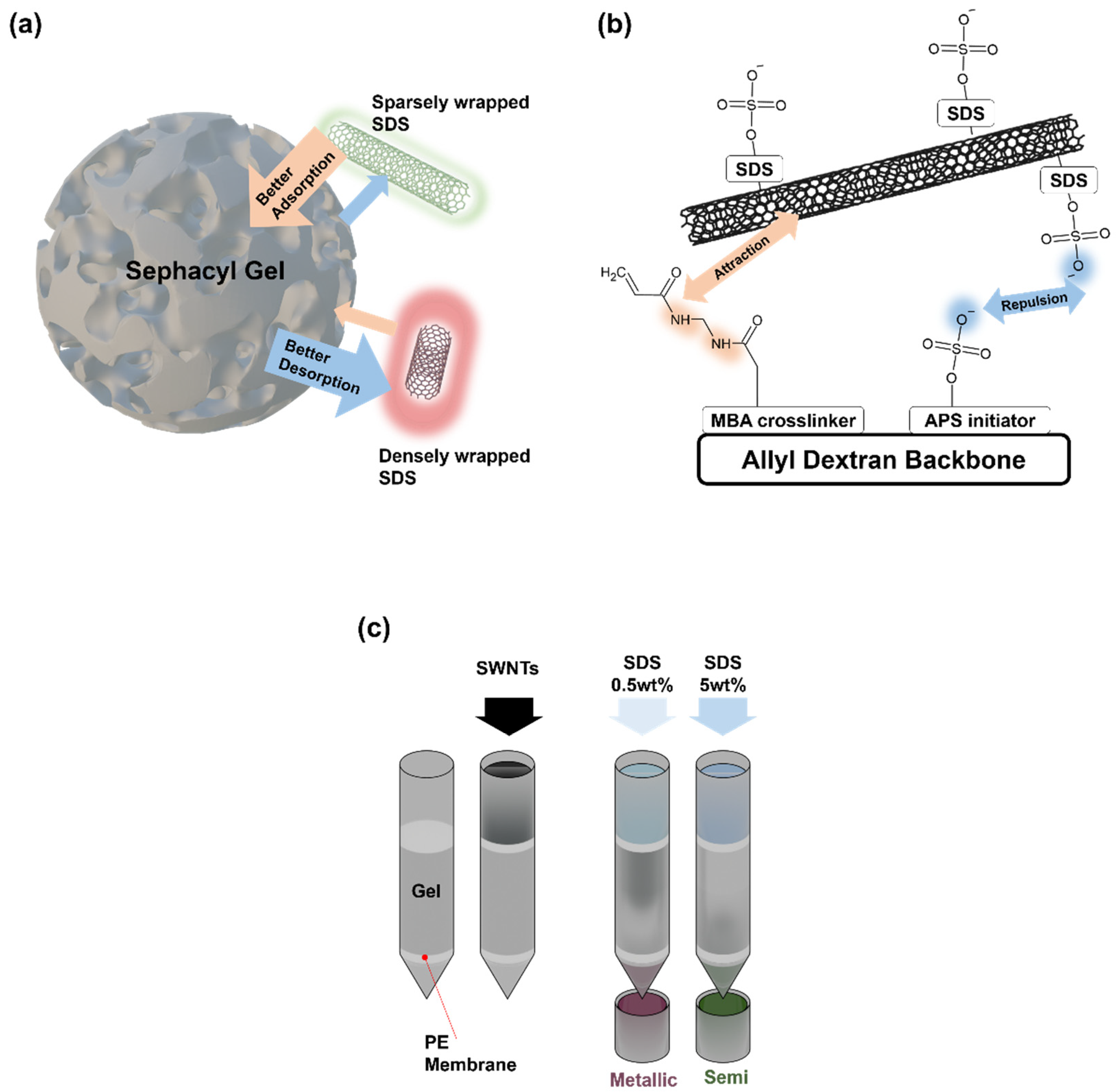
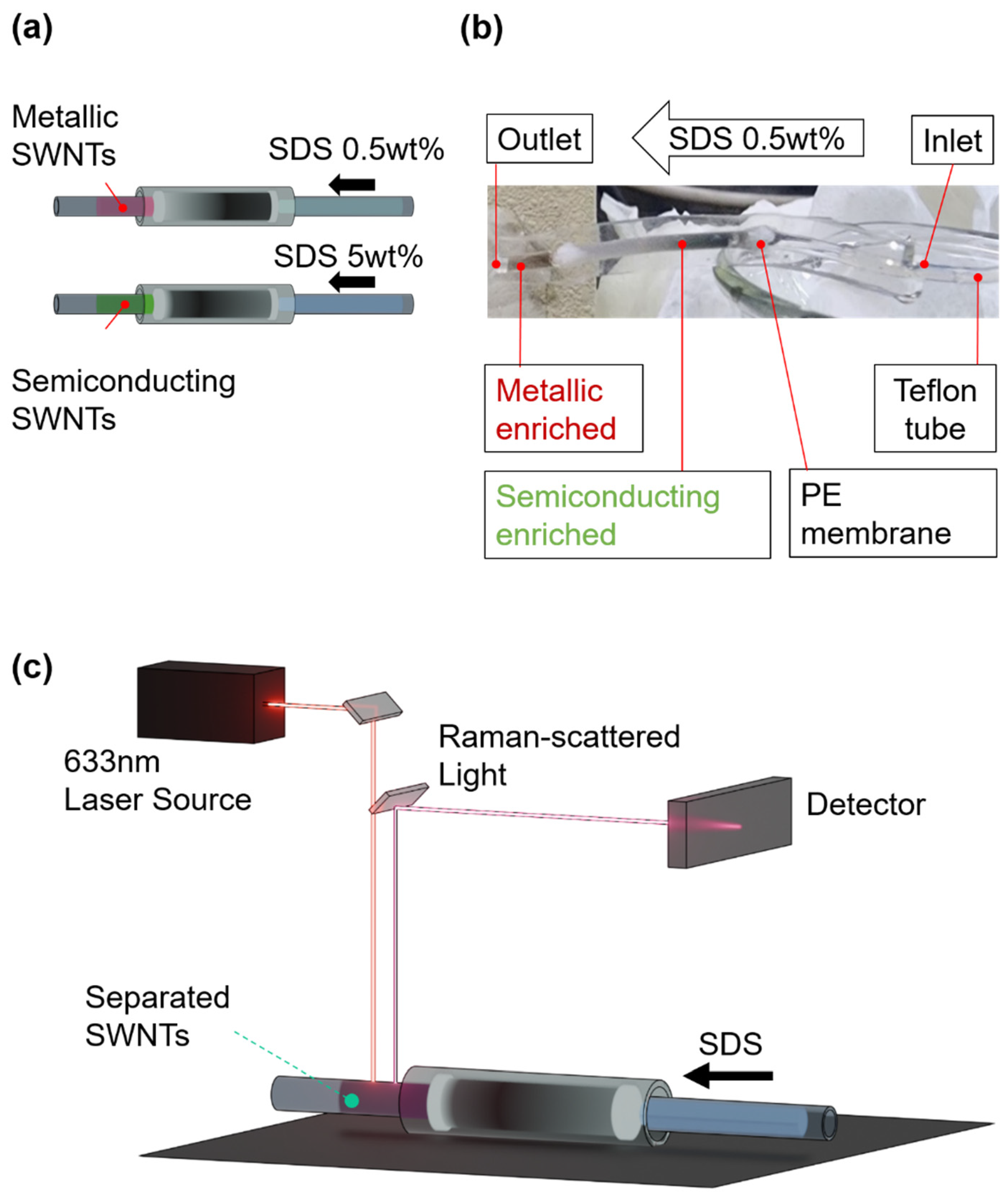
The efficient separation of metallic and semiconducting SWNTs was achieved using a PDMS-based microfluidic gel chromatography column, as depicted in Figure 4a. The process involved injecting sodium dodecyl sulfate (SDS) at two distinct concentrations: 0.5 wt% SDS for metallic SWNTs and 5 wt% SDS for semiconducting SWNTs. This approach capitalized on the differential interactions between SWNTs and the gel matrix, driven by the variation in repulsion forces mediated by SDS concentration. The stepwise elution enabled clear differentiation between metallic and semiconducting SWNT fractions. The visual contrast between the separated fractions was striking, as shown in Figure 4b. Metallic SWNTs, characterized by their weaker interactions with SDS, exhibited a reddish appearance, whereas semiconducting SWNTs, with stronger gel affinities, displayed a greenish color. This color distinction underscores the precision of the separation method and aligns with the inherent optical properties of HiPco SWNTs. The reddish tint of metallic SWNTs and the greenish tint of semiconducting SWNTs were consistent with prior observations, reaffirming the effectiveness of SDS-mediated chromatographic separation [19].
Post-separation analysis of the SWNT fractions was conducted using in-situ Raman spectroscopy, as shown in Figure 4c, to precisely determine their electronic structure. The method leveraged the radial breathing mode (RBM) vibrations in the range of 100–300 cm⁻¹, which are highly sensitive to the diameter and electronic properties of SWNTs. RBM peaks below 250 cm⁻¹ were attributed to metallic SWNTs, while those above this threshold corresponded to semiconducting SWNTs, providing a clear distinction between the two types. To avoid laser-induced disruptions such as heating or photon-induced energy effects, the Raman measurements were performed on SWNT fractions flowing through a Teflon tube connected to the microfluidic column. This approach reinforced the reliability of the microfluidic gel chromatography system in achieving efficient separation and accurate electronic characterization, offering significant insights into SWNT properties for advanced nanomaterial analysis.
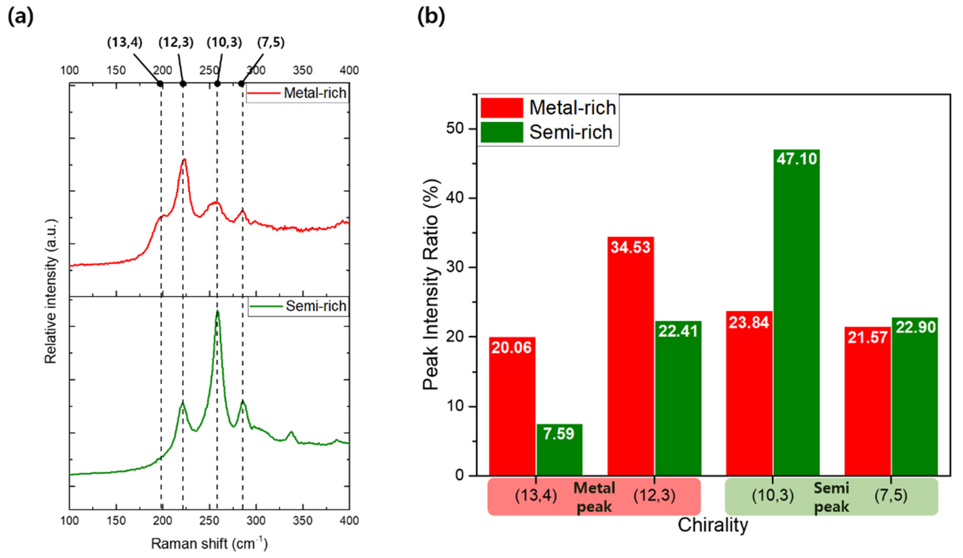
Figure 5a presents the Raman spectra of the metallic-enriched (reddish) and semiconducting-enriched (greenish) samples, highlighting significant differences in the four primary peaks: 197 cm⁻¹ for metallic (13,4), 217 cm⁻¹ for metallic (12,3), 255 cm⁻¹ for semiconducting (10,3), and 284 cm⁻¹ for semiconducting (7,5). The distinct RBM peaks observed for these chiralities confirm the successful separation, as the metallic and semiconducting SWNTs exhibit characteristic vibrational modes corresponding to their respective structural configurations. The intensity and position of these peaks provide insight into the composition and purity of the separated samples, with metallic SWNTs showing more prominent low-frequency RBM peaks compared to their semiconducting counterparts. In the metal-rich sample, the (12,3) metallic peak was particularly prominent, indicating a higher concentration of metallic SWNTs with this specific chirality. In contrast, the semi-rich sample exhibited distinct peaks for (10,3) and (7,5) semiconducting SWNTs, with only minor contributions from the (12,3) metallic SWNTs. This suggests that the separation process was effective in enriching the sample with semiconducting SWNTs while significantly reducing the presence of metallic SWNTs, thereby demonstrating the efficacy of the PDMS microchannel-based gel chromatography in achieving selective separation based on electronic properties.
Figure 5. (a) Raman spectra in the radial breathing mode (RBM) region for metallic-rich (top) and semiconducting-rich (bottom) SWNT samples, highlighting four distinct chirality peaks: (13,4), (12,3), (10,3), and (7,5). The vertical dashed lines indicate the Raman shifts corresponding to these chiralities. (b) Relative peak intensity ratios (%) for the four chiralities, comparing metallic-rich and semiconducting-rich fractions. The differences in intensity ratios demonstrate the effectiveness of the separation process in enriching SWNTs based on their electronic type.
Preprints 141654 g005
Figure 5b provides a comprehensive comparison of the relative ratios of the four major Raman peaks between the metallic-enriched and semiconducting-enriched SWNT samples. Peaks associated with metallic chiralities, specifically (13,4) and (12,3) SWNTs, were more prominent in the metallic-rich samples. Conversely, peaks linked to semiconducting chiralities, such as (10,3) and (7,5) SWNTs, exhibited higher relative intensities in the semiconducting-enriched samples. Notably, while the (7,5) peak in semiconducting-enriched samples was only marginally more intense than in metallic-enriched samples, the (10,3) peak showed a substantial increase in intensity, underscoring the selective enrichment of semiconducting SWNTs. Through analysis of the RBM region, these measurements confirm that the separation process effectively altered the relative proportions of metallic and semiconducting SWNTs across the different sample fractions. The observed shift in peak ratios across separated samples highlights the capacity of this micro-sized PDMS column-based gel chromatography system to achieve selective isolation based on SWNT chirality and electronic properties.
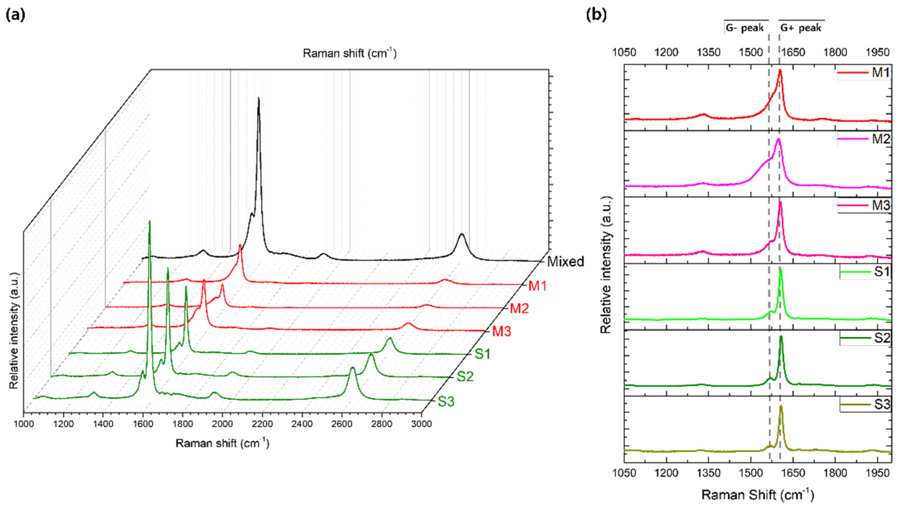
Furthermore, the separated SWNT samples were examined for variations in their G peak profiles, as illustrated in Figure 6. The G peak, a hallmark of sp²-hybridized carbon structures, provides valuable information on the electronic characteristics of SWNTs. It is typically split into two components: the G⁻ peak, observed around 1560 cm⁻¹, and the G⁺ peak, located near 1590 cm⁻¹ [20]. The G⁻ peak is associated with atomic vibrations along the nanotube axis, whereas the G⁺ peak corresponds to vibrations in the circumferential direction. In metallic SWNTs, the G⁻ peak is typically broader due to the influence of free electrons, while in semiconducting SWNTs, it appears sharper and more defined, reflecting the absence of free carriers [21]. Figure 6a provides an overview of the Raman spectra, showing the D, G, and G’ peaks across all separated samples. This spectral profile displays the progressive evolution from mixed SWNTs to metal-enriched (M1–M3) and semi-enriched (S1–S3) fractions, facilitating a comparative analysis of the relative intensities at various Raman shifts. This visual comparison highlights the distinct separation of metallic and semiconducting SWNT components achieved through the process. Specifically, Figure 6b offers a close-up of the G peaks, where the G⁻ and G⁺ components show noticeable shifts and shape changes across the samples, further evidencing the separation. The elution fractions collected at different stages were labeled as M1, M2, M3 (for metallic SWNTs) and S1, S2, S3 (for semiconducting SWNTs). In Figure 6b, a clear trend is visible in the G⁻ peak profiles, evolving from a broad shape in M1 to a sharp form in S3, which indicates a continuous enrichment of semiconducting SWNTs through the separation process. The broader G⁻ peaks observed in the M1, M2, and M3 samples underscore their metallic nature, while the progressively narrow G⁻ peaks in S1, S2, and S3 confirm the increasing purity of semiconducting SWNTs in these later fractions.
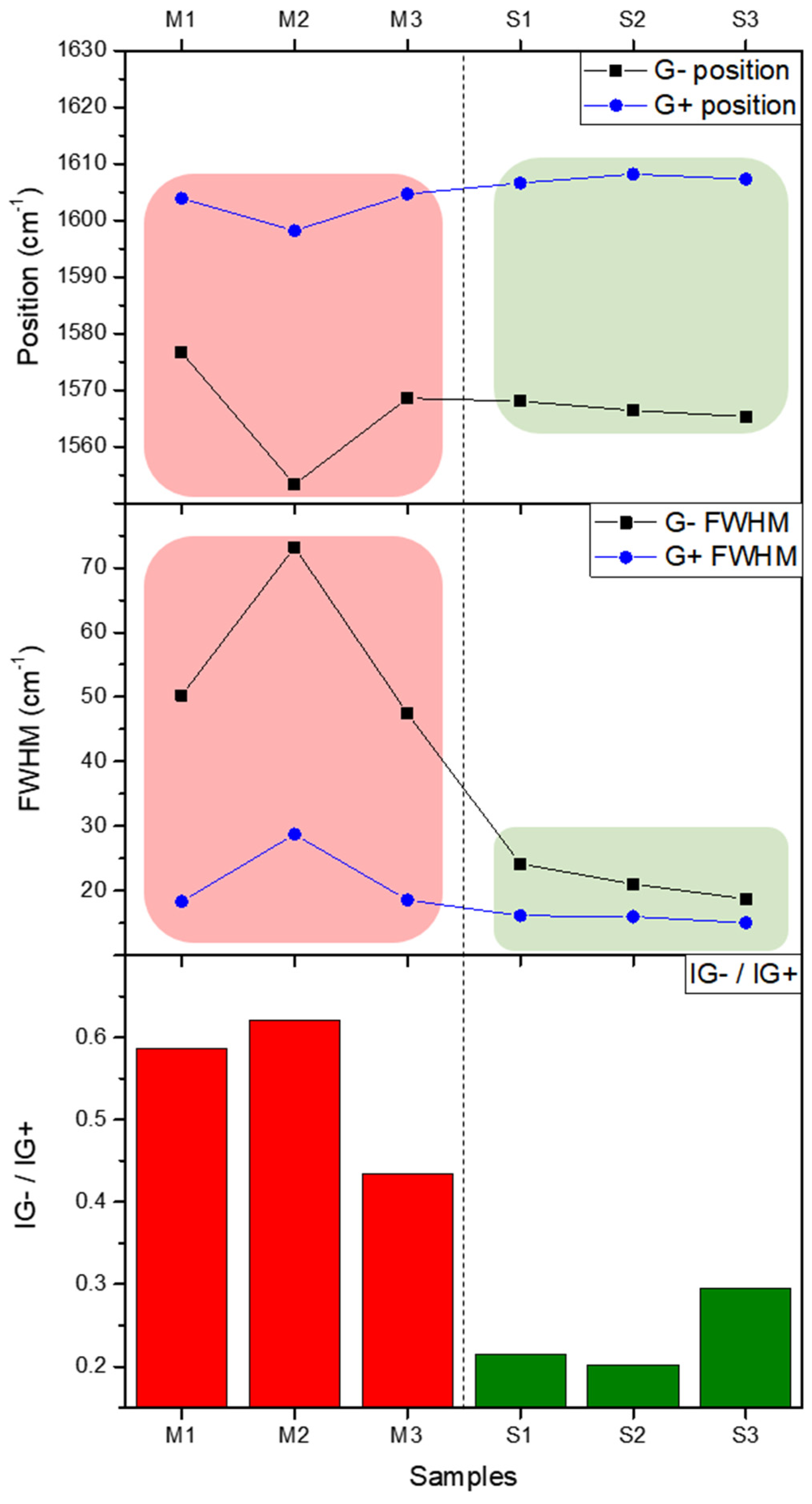
To quantify the separation efficiency, the full width at half maximum (FWHM) of the G⁻ peaks was measured, as summarized in Table 1. Metallic-enriched fractions (M1, M2, M3) exhibited broader G⁻ peaks, with full width at half maximum (FWHM) values between 47.45 and 73.17 cm⁻¹, reflecting a heterogeneous electronic composition. The broadening and asymmetry observed in the G⁻ peaks for metallic SWNTs are characteristic of the Breit-Wigner-Fano (BWF) band, which arises from electron-phonon coupling and the interaction between discrete phonon states and electronic continuum [22,23,24]. This behavior is unique to metallic SWNTs and further highlights their distinct electronic properties compared to semiconducting SWNTs. In contrast, the semiconducting-enriched fractions (S1, S2, S3) displayed narrower G⁻ peaks, with FWHM values ranging from 18.75 to 24.21 cm⁻¹, which is consistent with a well-defined electronic structure. Fractions eluted with 5 wt% SDS (S1, S2, S3) showed FWHM values that were approximately half those of fractions eluted with 0.5 wt% SDS (M1, M2, M3). The reduction in FWHM across sequential samples highlights the progressive isolation of semiconducting SWNTs. The difference in peak positions between metallic and semiconducting SWNTs further corroborates the successful separation. Generally, metallic SWNTs with identical diameters exhibit G⁻ peaks at lower positions than semiconducting SWNTs [20]. However, as shown in Table 1, metallic samples M1 and M3 had higher G⁻ peak positions than some semiconducting samples, likely due to the presence of SWNTs with varying diameters, as suggested by the RBM peaks in Figure 4. Previous studies indicate that smaller-diameter SWNTs, which correspond to RBM peaks at higher wavenumbers, tend to display G⁻ peaks at lower wavenumbers [20,21]. The samples separated with 5 wt% SDS in Figure 4 exhibited RBM peaks at larger wavenumbers than those separated with 0.5 wt% SDS, suggesting that the G⁻ peaks in S1, S2, and S3 are influenced by SWNT diameter. Additionally, the intensity of G for each sample was divided by the intensity of G+ to represent the relative ratio of the two peak intensities. M1, M2, and M3 showed values ranging between 0.43 and 0.62, while S1, S2, and S3 exhibited relatively lower values, ranging between 0.20 and 0.30.
Figure 7. Position, FWHM, and relative intensity ratio of G⁻ and G⁺ peaks are compared across separated SWNT samples (M1–M3 for metallic-rich, S1–S3 for semiconducting-rich fractions). The upper panel illustrates the G⁻ and G⁺ peak positions, highlighting systematic shifts due to electronic differences. The middle panel presents the FWHM for G⁻ and G⁺ peaks, showing broader G⁻ peaks for metallic-rich fractions. The lower panel depicts the G⁻/G⁺ intensity ratio, which decreases progressively from metallic-rich to semiconducting-rich fractions, offering a clear metric for distinguishing electronic types in SWNTs.
Preprints 141654 g007
The trends of G⁻ and G⁺ in the metallic and semiconducting samples are summarized in Figure 6, offering a comprehensive overview of the separation efficiency achieved via microfluidic gel chromatography combined with in-situ Raman spectroscopy, as described in this study. The degree of separation is evident in the distinct differences in peak position, FWHM, and the relative intensity ratio (IG⁻/IG⁺), all of which clearly distinguish the electronic and structural characteristics of the two SWNT types. In particular, the pronounced broadening in the FWHM of G⁻ and the marked variations in IG⁻/IG⁺ ratios confirm the effectiveness of the microchannel-enabled separation technique. In the upper panel, the G⁻ peak positions for metallic-enriched fractions (M1, M2, M3) are systematically lower than those for semiconducting-enriched fractions (S1, S2, S3). This trend arises from the unique electronic density of states near the Fermi level in metallic SWNTs, underscoring the fundamental impact of electronic type on Raman spectral features. In contrast, the G⁺ peak remains relatively stable across all fractions, demonstrating its independence from electronic properties. The middle panel emphasizes the striking contrast in the FWHM of G⁻ peaks between the two types of SWNTs. The broader and more asymmetric G⁻ peaks in the metallic fractions, with FWHM values ranging from 47.45 to 73.17 cm⁻¹, reflect the influence of the BWF line shape caused by electron-phonon coupling. By comparison, the semiconducting fractions exhibit narrower G⁻ peaks (18.75–24.21 cm⁻¹), indicative of their uniform electronic structure and the progressive isolation achieved during separation. In the lower panel, the relative intensity ratio (IG⁻/IG⁺) serves as a robust metric for differentiating metallic and semiconducting fractions. Metallic-enriched samples display significantly higher ratios (0.43–0.62), consistent with the dominance of the broadened G⁻ peak, whereas semiconducting-enriched fractions show much lower ratios (0.20–0.30), reflecting their distinct Raman characteristics. These observations collectively validate the microfluidic gel chromatography-enabled in-situ Raman spectroscopy approach for selective electronic-type separation and analysis of SWNTs. Not only does this methodology effectively isolate metallic and semiconducting SWNTs, but it also reveals subtle vibrational and electronic interactions inherent to each type. The pronounced differences in G peak characteristics—spanning position, width, and intensity ratio—underscore the critical role of electron-phonon interactions and diameter variation in defining the Raman spectral behavior of SWNTs.
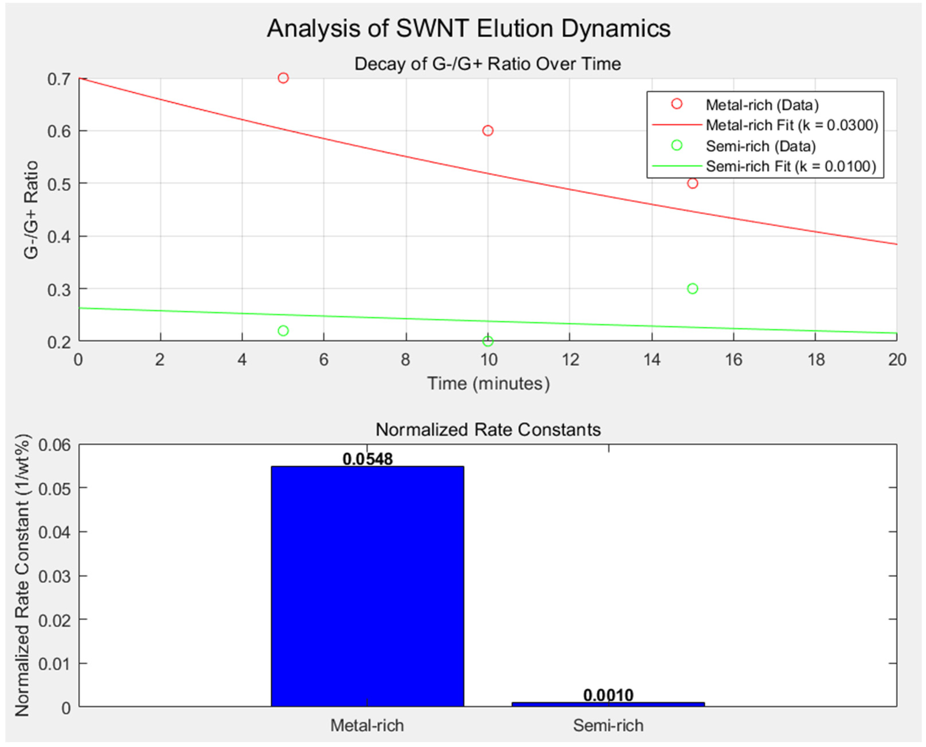
Figure 8 provides an integrated view of the elution dynamics and separation characteristics of metallic- and semiconducting-enriched SWNT fractions. The analysis is based on the G⁻/G⁺ intensity ratio measured from Raman spectroscopy for M1–M3 (metal-rich, SDS 0.5 wt%) and S1–S3 (semi-rich, SDS 5 wt%) samples. These values were analyzed over time to calculate rate constants for elution and assess SWNT purity, while accounting for the differing SDS concentrations used during separation.
Methodology for Rate Constant Calculation
To derive the rate constants, the decay in the G⁻/G⁺ intensity ratio over time was modeled using a single exponential decay function, assuming that the elution dynamics follow a first-order process. The measured data were fit to the Equation (1):
Preprints 141654 i001
where, Preprints 141654 i002 is the G⁻/G⁺ intensity ratio at time t, Preprints 141654 i003 is the initial ratio, and k is the rate constant of elution. For metallic-rich fractions (M1–M3), the decay dynamics yielded, kmetal = 0.0300 min−1, reflecting their rapid elution due to weaker interactions with the gel matrix. In contrast, the semiconducting-rich fractions (S1–S3) exhibited ksemi = 0.0100 min−1, which aligns with their stronger retention influenced by increased SDS-mediated gel interactions. The larger rate constant for the metallic fractions reflects their faster elution, consistent with weaker interaction with the gel matrix compared to semiconducting SWNTs.
Normalization of Rate Constants
To account for the 10-fold difference in SDS concentration between metallic- and semiconducting-enriched fractions (0.5 wt% vs. 5 wt%), the rate constants were normalized using the Equation (2):
Preprints 141654 i004
where, [SDS] is the SDS concentration in wt%. The normalization yielded knormalized,metal = 0.0548 min−1·wt−1% and knormalized,semi = 0.0010 min−1·wt−1%, highlighting the distinct separation dynamics for each SWNT type.
The upper panel of Figure 8 illustrates the decay of the G⁻/G⁺ ratio over time for both metallic- and semiconducting-enriched fractions. The metallic-rich fractions exhibit a steeper decay curve, indicative of faster elution rates. In contrast, the semiconducting-rich fractions show a more gradual decay, consistent with their stronger interaction with the gel matrix due to electronic differences. The lower panel of Figure 8 presents the normalized rate constants, emphasizing the intrinsic elution dynamics independent of SDS concentration. The higher normalized rate constant for metallic-rich SWNTs reflects their weaker van der Waals interaction with the gel matrix, while the lower value for semiconducting-rich SWNTs underscores their stronger retention due to greater gel affinity. The clear separation of rate constants between metallic- and semiconducting-enriched fractions correlates with their respective purities. The purity of each fraction is closely tied to the elution dynamics, as faster elution typically corresponds to lower gel-matrix interaction and higher metallicity. Conversely, the slower elution of semiconducting SWNTs aligns with their greater affinity for the gel and higher electronic uniformity. These findings validate the use of G⁻/G⁺ ratio decay as a reliable metric for quantifying SWNT separation efficiency and purity. This analysis demonstrates the effectiveness of the microfluidic gel chromatography approach for achieving precise electronic-type separation of SWNTs. It further underscores the importance of considering both experimental parameters (e.g., SDS concentration) and intrinsic SWNT properties when interpreting rate constants and purity metrics.

4. Conclusion

In this study, we introduced and validated an innovative PDMS-based microchannel system that enhances conventional gel chromatography methodologies for the precise microscale separation of SWNTs. By leveraging the selective interactions between SWNTs, the dispersant, and the gel matrix, the platform enabled the sequential isolation of metallic and semiconducting SWNTs with high accuracy. This separation process was quantitatively validated using G⁻/G⁺ intensity ratios and spectral shifts in G-band features, with rate constants providing critical insights into the elution dynamics for each SWNT type. The analysis revealed distinct trends in rate constants, normalized to the SDS concentration, which highlighted the faster elution kinetics for metallic-rich fractions compared to the semiconducting-rich counterparts, further supporting the platform’s capability to differentiate SWNTs by their electronic type.
This work marks a significant advancement in the integration of gel chromatography with a microfluidic framework, specifically tailored for SWNT separation at the nanoscale. Notably, the observed differences in normalized rate constants, alongside the systematic reduction in G⁻/G⁺ ratios over time, reflect the intricate interplay between SWNT electronic properties and their retention behaviors within the gel medium. The ability of the PDMS microchannel system to offer real-time insights into separation dynamics, coupled with its scalability, underscores its potential as a robust tool for both fundamental studies and industrial applications. The adaptability of the PDMS platform for channel fabrication and its compatibility with spectroscopic monitoring provide a unique avenue for refining separation processes and optimizing conditions for nanomaterial purification. By bridging the gap between large-scale industrial needs and microscale precision, this study establishes a foundational approach for developing advanced chromatographic technologies that address the challenges of SWNT purification. With continued optimization, this PDMS microchannel-based methodology is poised to significantly impact both research and applied domains, offering a scalable, efficient, and precise solution to the complex demands of nanomaterial separation.

5. Patents

Method for separating of single wall carbon nanotubes [KR Patent Application No. 10-2024-0077633].

Supplementary Materials

The following supporting information can be downloaded at the website of this paper posted on Preprints.org, which includes the detailed mathematical relationship between the chirality of single-walled carbon nanotubes (SWNTs) and their structural parameters utilized in the main text.

Author Contributions

Conceptualization, J.-H.H., B.B, S.J. and W.J.; methodology, J.-H.H., B.B., S.J. and W.J.; validation, B.B., S.J., W.J., J.W., J.J., Y.-J.C. and M.-K.M.; formal analysis, B.B., S.J. and W.J.; investigation, B.B., S.J., W.J., J.W., J.J., Y. -J.C. and M.-K.M.; writing—original draft preparation, J.-H.H., B.B., S.J. and W.J.; writing—review and editing, J.-H.H., B.B., S.J. and W.J.; visualization, B.B., S.J. and W.J.; supervision, J.-H.H.; project administration, J.-H.H.; funding acquisition, J.-H.H.

Funding

This work was supported by the Gachon University research fund of 2019(GCU-2019-0834). This work was also supported by Korea Institute for Advancement of Technology (KIAT) grant funded by the Korea Government (MOTIE) (No. P0012453, The Competency Development Program for Industry Specialist).

Data Availability Statement

The original contributions presented in the study are included in the article, further inquiries can be directed to the corresponding author.

Conflicts of Interest

The authors declare no conflicts of interest.

References

  1. Iijima, S. Helical microtubules of graphitic carbon. Nature 1991, 354(6348), 56–58. [Google Scholar] [CrossRef]
  2. Kalamkarov, A. L.; Georgiades, A. V.; Rokkam, S. K.; Veedu, V. P.; Ghasemi-Nejhad, M. N. Analytical and numerical techniques to predict carbon nanotubes properties. International Journal of Solids and Structures 2006, 43(22-23), 6832–6854. [Google Scholar] [CrossRef]
  3. Odom, T. W.; Huang, J.-L.; Kim, P.; Lieber, C. M. Structure and Electronic Properties of Carbon Nanotubes. J. Phys. Chem. B 2000, 104(13), 2794–2809. [Google Scholar] [CrossRef]
  4. Landi, B. J.; Ganter, M. J.; Cress, C. D.; DiLeo, R. A.; Raffaelle, R. P. Carbon nanotubes for lithium ion batteries. Energy Environ. Sci. 2009, 2(6), 638. [Google Scholar] [CrossRef]
  5. Javey, A.; Guo, J.; Farmer, D. B.; Wang, Q.; Wang, D.; Gordon, R. G.; Lundstrom, M.; Dai, H. Carbon Nanotube Field-Effect Transistors with Integrated Ohmic Contacts and High-κ Gate Dielectrics. Nano Lett. 2004, 4(3), 447–450. [Google Scholar] [CrossRef]
  6. Javey, A.; Guo, J.; Wang, Q.; Lundstrom, M.; Dai, H. Ballistic carbon nanotube field-effect transistors. Nature 2003, 424(6949), 654–657. [Google Scholar] [CrossRef] [PubMed]
  7. Wu, B.; Geng, D.; Liu, Y. Evaluation of metallic and semiconducting single-walled carbon nanotube characteristics. Nanoscale 2011, 3(5), 2074. [Google Scholar] [CrossRef]
  8. Rao, C. N. R.; Voggu, R.; Govindaraj, A. Selective generation of single-walled carbon nanotubes with metallic, semiconducting and other unique electronic properties. Nanoscale 2009, 1(1), 96. [Google Scholar] [CrossRef]
  9. Wang, C.; Takei, K.; Takahashi, T.; Javey, A. Carbon nanotube electronics – moving forward. Chem. Soc. Rev. 2013, 42(7), 2592–2609. [Google Scholar] [CrossRef]
  10. Wei, X.; Li, S.; Wang, W.; Zhang, X.; Zhou, W.; Xie, S.; Liu, H. Recent Advances in Structure Separation of Single-Wall Carbon Nanotubes and Their Application in Optics, Electronics, and Optoelectronics. Advanced Science 2022, 9(14), 2200054. [Google Scholar] [CrossRef]
  11. Hirano, A.; Tanaka, T.; Kataura, H. Thermodynamic Determination of the Metal/Semiconductor Separation of Carbon Nanotubes Using Hydrogels. ACS Nano 2012, 6(11), 10195–10205. [Google Scholar] [CrossRef]
  12. Zanoni, S.; Watts, B. P.; Tvrdy, K. Single-Walled Carbon Nanotube Chiral Selectivity Exhibited by Commercially Available Hydrogels of Varying Composition. ACS Appl. Mater. Interfaces 2021, 13(28), 33635–33643. [Google Scholar] [CrossRef]
  13. Liu, H.; Nishide, D.; Tanaka, T.; Kataura, H. Large-scale single-chirality separation of single-wall carbon nanotubes by simple gel chromatography. Nat Commun 2011, 2(1), 309. [Google Scholar] [CrossRef]
  14. Abdelgawad, M.; Wu, C.; Chien, W.-Y.; Geddie, W. R.; Jewett, M. A. S.; Sun, Y. A fast and simple method to fabricate circular microchannels in polydimethylsiloxane (PDMS). Lab Chip 2011, 11(3), 545–551. [Google Scholar] [CrossRef] [PubMed]
  15. Raj M, K.; Chakraborty, S. PDMS microfluidics: A mini review. J of Applied Polymer Sci 2020, 137(27), 48958. [Google Scholar] [CrossRef]
  16. Dolan, M.; Watts, B. P.; Tvrdy, K. Tailored synthesis of hydrogel media for chirality separation of single walled carbon nanotubes. Carbon 2021, 171, 597–609. [Google Scholar] [CrossRef]
  17. An, H. J.; Kim, S.; Seo, H.; Yoo, P. J.; Kim, W.-J. Simultaneous separation of high-purity semiconducting and metallic single-walled carbon nanotubes by surfactant concentration-controlled gel chromatography. Applied Surface Science 2020, 508, 145258. [Google Scholar] [CrossRef]
  18. Blanch, A. J.; Quinton, J. S.; Shapter, J. G. The role of sodium dodecyl sulfate concentration in the separation of carbon nanotubes using gel chromatography. Carbon 2013, 60, 471–480. [Google Scholar] [CrossRef]
  19. Yanagi, K.; Miyata, Y.; Tanaka, T.; Fujii, S.; Nishide, D.; Kataura, H. Colors of carbon nanotubes. Diamond and Related Materials 2009, 18(5-8), 935–939. [Google Scholar] [CrossRef]
  20. Gao, B.; Zhang, Y.; Zhang, J.; Kong, J.; Liu, Z. Systematic Comparison of the Raman Spectra of Metallic and Semiconducting SWNTs. J. Phys. Chem. C 2008, 112(22), 8319–8323. [Google Scholar] [CrossRef]
  21. Dresselhaus, M. S.; Dresselhaus, G.; Hofmann, M. The big picture of Raman scattering in carbon nanotubes. Vibrational Spectroscopy 2007, 45(2), 71–81. [Google Scholar] [CrossRef]
  22. Wu, Y.; Maultzsch, J.; Knoesel, E.; Chandra, B.; Huang, M.; Sfeir, M. Y.; Brus, L. E.; Hone, J.; Heinz, T. F. Variable Electron-Phonon Coupling in Isolated Metallic Carbon Nanotubes Observed by Raman Scattering. Physical Review Letters 2007, 99(2), 027402. [Google Scholar] [CrossRef] [PubMed]
  23. Farhat, H.; Son, H.; Samsonidze, G. G.; Reich, S.; Dresselhaus, M. S.; Kong, J. Phonon Softening in Individual Metallic Carbon Nanotubes due to the Kohn Anomaly. Physical Review Letters 2007, 99(14), 145506. [Google Scholar] [CrossRef] [PubMed]
  24. Dresselhaus, M.; Jorio, A.; Saito, R. Characterizing graphene, graphite, and carbon nanotubes by Raman spectroscopy. Annu. Rev. Condens. Matter Phys. 2010, 1(1), 89–108. [Google Scholar] [CrossRef]
Figure 2. (a) Schematic representation of the SDS-SWNT-gel system and the separation mechanism employed in gel chromatography. (a) The extent of SDS wrapping influences the interaction of SWNTs with the Sephacryl gel. Sparsely wrapped SWNTs (green) exhibit enhanced adsorption due to reduced repulsive forces, while densely wrapped SWNTs (red) desorb more readily because of stronger repulsion. (b) Molecular structure of the Sephacryl gel, illustrating functional groups derived from the MBA crosslinker and APS initiator attached to an allyl dextran backbone. These functional groups create a balance of attractive and repulsive forces that selectively interact with SDS-wrapped SWNTs. (c) Conventional gel chromatography process, demonstrating the sequential separation of metallic and semiconducting SWNTs by modulating SDS concentrations (0.5 wt% for metallic SWNTs and 5 wt% for semiconducting SWNTs). This process enables precise differentiation of SWNT types based on their electronic properties.
Preprints 141654 g002
Figure 3. Schematic representation of the fabrication and assembly process for the microfluidic gel chromatography column system using a PDMS mold. The process involves molding the microchannel with a wire template, integrating a polyethylene (PE) membrane to retain the gel, and connecting Teflon tubes for fluid injection. The assembled microchannel enables precise control for SWNT separation via SDS-based gel chromatography.
Preprints 141654 g003
Figure 4. (a) Schematic of the microfluidic gel chromatography process used for the separation of metallic and semiconducting SWNTs within a PDMS-based column. The separation was achieved by sequentially injecting SDS dispersant solutions at 0.5 wt% and 5 wt%, facilitating the elution of metallic and semiconducting SWNTs, respectively. (b) Photographic evidence of the separated SWNT fractions at the outlet, where metallic SWNTs exhibited a reddish color and semiconducting SWNTs appeared greenish, demonstrating the effectiveness of the separation process. (c) Experimental setup for in-situ Raman spectroscopy analysis conducted downstream of the microfluidic column, illustrating the in-situ characterization of SWNTs via a 633 nm laser source and detector system. The Raman setup enables precise analysis of electronic types based on radial breathing mode (RBM) signals without disrupting the chromatographic environment.
Preprints 141654 g004
Figure 6. (a) Raman spectra comparing metallic-rich (M1–M3) and semiconducting-rich (S1–S3) SWNT fractions across a broad spectral range, including the D, G, and G’ peaks. The stacked plot highlights distinct spectral features corresponding to each separated fraction. (b) Zoomed-in view of the G peaks, emphasizing the G⁻ and G⁺ components for each sample. The differences in peak positions and shapes between metallic-rich and semiconducting-rich fractions illustrate the separation’s effectiveness and the electronic-type-specific interactions during the elution process.
Preprints 141654 g006
Figure 8. Analysis of SWNT elution dynamics based on the G⁻/G⁺ intensity ratio. The upper panel displays the decay of G⁻/G⁺ ratio over time for metallic-rich (M1–M3) and semiconducting-rich (S1–S3) fractions, fitted to an exponential decay model. The rate constants (k) for each fraction, normalized to SDS concentration, are shown in the lower panel as bar charts, indicating faster elution rates for metallic-rich fractions. The results highlight the effectiveness of microfluidic gel chromatography in isolating SWNT fractions by electronic properties while reflecting SDS-driven retention dynamics.
Preprints 141654 g008
Table 1. Peak positions and full width at half maximum (FWHM) values for the G⁻ and G⁺ peaks of metallic-rich (M1, M2, M3) and semiconducting-rich (S1, S2, S3) SWNT fractions. The intensity ratio between G⁻ and G⁺ peaks (G⁻/G⁺) is also included for each sample, providing insights into the structural and electronic-type-specific characteristics of the separated SWNTs. Each sample designation represents the sequential elution step during the separation process.
Separated
Samples
G- positon(cm-1) G+ position(cm-1) G- FWHM(cm-1) G+ FWHM(cm-1) Intensity ratio
G- / G+
M1 1576.65 1603.89 50.24 18.35 0.59
M2 1553.33 1598.18 73.17 28.74 0.62
M3 1568.54 1604.67 47.45 18.57 0.43
S1 1568.05 1606.63 24.21 16.17 0.22
S2 1566.39 1608.18 21.05 16.00 0.20
S3 1565.30 1607.31 18.75 15.04 0.30
Disclaimer/Publisher’s Note: The statements, opinions and data contained in all publications are solely those of the individual author(s) and contributor(s) and not of MDPI and/or the editor(s). MDPI and/or the editor(s) disclaim responsibility for any injury to people or property resulting from any ideas, methods, instructions or products referred to in the content.
Copyright: This open access article is published under a Creative Commons CC BY 4.0 license, which permit the free download, distribution, and reuse, provided that the author and preprint are cited in any reuse.
Prerpints.org logo

Preprints.org is a free preprint server supported by MDPI in Basel, Switzerland.

Subscribe

Disclaimer

Terms of Use

Privacy Policy

Privacy Settings

© 2025 MDPI (Basel, Switzerland) unless otherwise stated