
Submitted:
25 November 2024
Posted:
27 November 2024
You are already at the latest version
Abstract
This paper proposes a detailed design study of resonating high-frequency notch filters driven by RF MEMS switches and their optimization for dual-band operation in the X-Band. Microstrip configurations will be considered for single and dual-band applications. An SPDT (single-pole-double-thru) switch composed of double-clamped ohmic micro-switches has been introduced to connect triangular resonators with Sierpinski geometry, symmetrically placed with respect to a microstrip line, to obtain a dual notch response. Close frequencies or spans as wide as 2 GHz can be obtained depending on the internal complexity and the edge side.
Keywords:
RF MEMS
; SPDT
; microwaves
; dual-band operation
; triangular resonators
; Sierpinski geometry
1. Introduction
The utilization of fractal geometries for high-frequency signal processing has been a hot topic for a couple of decades, aiming to provide a multi-band response with reduced size and increasing geometrical complexity, either in planar or volume configurations. A review for antenna purposes is given by [1]. Often, these structures are inspired by a metamaterial design and the tunability is given by switching single components of the structure [2]. Moreover, by changing the fractal structure's complexity and the figure's planar extension, high-frequency applications can benefit from frequency tuning due to both characteristics. RF MEMS switches introduce a further advantage in the tuning performance, addressing the signal to routes characterized by different operative frequencies [3,4,5]. The above solution has been studied by combining single microswitches in a single-pole-double-thru (SPDT) structure to obtain devices in coplanar waveguide (CPW) configurations with CPW-based notch filters driven by RF MEMS SPDT switches [6]. Sierpinski-inspired triangular resonators with a CPW arrangement have also been studied in [7]. Advantages coming from the symmetric configuration of the resonators with respect to the feeding line have been outlined, as well as the general benefits in terms of quality factor, footprint, and operational frequency increase due to a triangular shape compared to square and circular geometries [8].
In this paper, a microstrip configuration has been chosen as an alternative to the CPW ones, with the advantage of a less critical design because the role played by the lateral ground plane is now absent, and a simple λ/4 transformer has been used to account for the operative frequencies of the designed resonators to address the signal and match the device adequately. Individual resonators have been optimized by changing the distance between the triangle and the microstrip line, finding that the optimal distance depends on the internal complexity of the Sierpinski configurations. Simple analytical derivations of the resonance frequency agree with the simulated responses of the whole triangles, and a trend of resonance for the Sierpinski triangles is a function of internal complexity. Finally, good electrical performances are predicted for the studied structures. All the simulations have been performed using Microwave Office (MWO) Axiem, release 17.
2. Microstrip Design of Single Sierpinski Resonators
Triangular Sierpinski resonators have been studied using a 50 ohm microstrip transmission line as the feeding line and searching for an optimal response of the notch filter corresponding to the best electrical matching of the resonator. In particular, the distance between the transmission line and the resonator has been changed to optimize the coupling. The substrate defined for the simulations is a high-resistivity silicon (HRS) wafer 640 µm thick, with 1 µm of silicon oxide on both sides, i.e., the typical thermal oxide thickness used before processing the substrate with patterning of the metal structures on one side. Considering the matching for the resonators feeding line, a 50 ohm line is obtained by imposing a 515 µm wide microstrip for a grounded 640 µm thick HRS.
After that, 6000 μm edge long triangles with internal complexity from 0 to 3, i.e., Sierpinski structures with internal triangles ranging from 1 (entire shape without holes) to 27 (3rd iteration in the internal subdivision), have been designed, with a grating of 200 μm separating each sub-element of the structure. The Sierpinski triangles are figures belonging to the more general group of fractals. They are obtained by a progressive subdivision of whole triangles into many internal triangles of decreasing size, as discussed in [9,10,11].The number of internal triangles is easily obtained by a law , where “n” is the internal complexity index. It must be noticed that a growing number of internal triangles corresponds to a vanishing area and a growing perimeter of the entire figure [12]. The four triangles chosen for the present study have been defined from C0 to C3, depending on the level of the complexity C.
The optimization has been performed by searching for the optimal distance between the resonator and microstrip, which is different for each shape, looking at the deepest peak in the two-port band-stop arrangement. This difference has been interpreted owing to the shape difference between the triangle edge and the microstrip transmission line, which is homogeneous and continuous only in the case of the C0 shape. Still, it is fragmented for C1, C2, and C3, significantly modifying the boundaries involved in the coupling, owing to the discontinuities introduced by a growing number of sub-triangles.
The symmetric configuration, with two triangles having the same geometry on both sides of the microstrip, guarantees a deeper peak to increase the quality factor of the resonator and a more homogeneous distribution of the electromagnetic field around the entire structure, thus not allowing the generation of additional spurious modes in the spectral response of the resonators, as it has also been discussed in [8].
Figure 1 (a) and (b) present the resonator layout for the C0 configuration and the transmission coefficient S21 obtained after the structure was simulated using MWO. The triangle has an edge a=6 mm long, while the microstrip exceeds the resonator size by 3 mm on each side.
It is evident from Figure 1 (b) that the deepest peak is obtained by imposing a distance of 200 µm between the microstrip and the two symmetric triangles. The C0 configuration has also been studied by changing the side length of the triangle and fixing the distance with respect to the microstrip, also maintaining the I/O lines 3 mm long. This procedure is another way to obtain different resonance frequencies, which is well-established from the resonators and patch antenna theory. It has to be noticed that good electrical matching is expected at least until the beginning of the K-Band. Additional simulations are needed to confirm that the same boundary geometric conditions can be extended to higher operative frequencies. The results of the preliminary simulations for possible K-Band extension are shown in Figure 2 for three triangular symmetric C0 configurations having edge lengths a=6000, 5200, and 4000 µm, respectively.
This preliminary evaluation is necessary to confirm the agreement between the original analytical approach to determine the resonance frequency, also in agreement with experimental results, and the performed electromagnetic simulation. The equation governing the resonance frequency of a triangular metallic shape on a substrate having dielectric constant ε is given by:
Where c=light speed, ε=dielectric constant, a=edge length, h=substrate thickness.
It is well known from the seminal works [13,14] that only the edge length must be corrected by an effective value, while the dielectric constant is the actual one of the substrate, as shown in Eqs. (1), which results in an effective resonance frequency value. A more detailed calculation was also performed in [15]. The comparison among the resonance frequencies is shown in Table 1, where a very good agreement is obtained using both approaches. The same method has been used for triangles with higher complexity, and the shape and the simulation results are shown in Figure 3, Figure 4, and Figure 5, respectively, for the main mode. The spectrum, including higher-order modes, was calculated in [13].
It is worth noting that the optimal matching is obtained for a distance close to the microstrip when the complexity is “0”, while it exhibits an increase and a slow decrease for C1, C2, and C3 with values 400, 350 and 300 μm respectively. The “jump” could be justified by the sudden change in the amount of metal when C1 is excited, with a single big triangular hole. At the same time, the increase in complexity also generates an increase in the number of sub-triangles close to the microstrip, with an increasing superposition with the electromagnetic field near the resonators. The predicted resonance frequencies for the optimal resonators are collected in the following plot (Figure 6), where it is evident the role that will be played by resonators having the same footprint but different complexity: the C0 mixed with C1, C2 or C3 will generate a dual-band operation with frequencies quite far from each other, while an interplay using C1, C2, and C3 is better for fine-tuning. The trend of the resonance frequency as a function of complexity is shown in Figure 7.
Of course, we can obtain similar results by changing the resonator size. Still, it is more convenient to maintain a fixed footprint of the triangular patch, considering the possibility of combining the same elementary cell in more complicated filtering structures or antenna arrays.
3. Simulation of the dual-band Sierpinski Resonators driven by the RF MEMS SPDT
A single-pole-double-thru (SPDT) switch has already been used in the study of coplanar waveguide (CPW) resonating structures made by Sierpinski triangles to select two possible frequencies corresponding to two different resonators placed at the output of ports 2 and 3 of the SPDT, fed by a microwave signal coming from the port 1. The SPDT was designed and manufactured using microsystem technology and RF MEMS switches to obtain the desired port for the output signal. In the previous case, the bridges were ohmic structures in a CPW environment, causing the passage of the high-frequency signal when a suspended metal beam is actuated using an electrostatic force provided by a DC signal feeding the switch to cause its collapse for a threshold voltage [6]. In this case, the mechanical functionality and the kind of electrical contact remain unchanged, but the lateral ground planes have been removed, and the structure has been transformed into a microstrip configuration. Considering the predicted frequencies of operation for the resonators to be connected, a simple λ/4 transformer has been used, working primarily between 7.5 GHz and 9.5 GHz. Even in a 2 GHz frequency range, the SPDT exhibits a reasonable response, which is helpful for a low-loss device within the X-Band. The configuration includes two switches and three arms with a transformer for each port, and its configuration and electrical performance for the output at port 2 are shown in Figure 8, when the switch before port 2 is actuated. The metal beam of the switch at port 3 is in the up position, providing the isolation for port 3. The symmetry of the structure guarantees the same result when the switch on port 3 is actuated (down position of the micromechanical bridge).
After optimizing the individual resonators and matching the SPDT in the X-Band, they have all been connected to obtain a frequency selector working on a dual-band base. In particular, C0 has been used with C1, C2, and C3 for tunability over an extended band, whereas C1, C2, and C3 have been connected to get tunability over a small bandwidth. The results are shown in the following figures. The interconnection has marginally changed the resonance frequencies, thus demonstrating the feasibility of a simple matching network to have the entire device working correctly.
Figure 9, Figure 10 and Figure 11 show the interconnections between C0 and the other three resonators with the simulated responses.
The above plots show a good response for selecting frequencies at approximately 2 GHz between them. Fine-tuning has been studied using the couples C1-C2, C1-C3, and C2-C3, plotting simulations in Figure 12, Figure 13 and Figure 14.
The above results show that the tuning becomes finer and finer as the internal complexity of the Sierpinski resonator increases. This result was also expected based on the individual responses of the resonators studied before. No criticalities have been observed in having a good electrical response in both situations, with excellent loss levels and peak depths of the notch filters.
4. Conclusions
This paper proposes a micromechanical device for dual-band applications using triangular Sierpinski resonators as notch filters selected utilizing an RF MEMS-based SPDT switch. A microstrip configuration was chosen for the exploited structures. This study was performed with a complexity of the fractal triangles up to the third order, compatible with typical sizes of a classical photolithographic process. First, the electrical performance of the individual resonators has been optimized for frequencies within the X-Band. Then, a λ/4 transformer was used to electrically match the three branches of the SPDT switch, connected to the optimized single resonators. The investigated structures exhibit interesting properties concerning the optimal distance between the resonator and the microstrip feeding line and the possibility of interconnecting triangles with different Sierpinski complexity to obtain fine-tuning of the frequency. It is worth noting that in the case of resonators (or possibly patch antennas), the size could be a solution for selecting different frequencies, but maintaining the same footprint is important in view of the design and realization of filters and antenna arrays exhibiting the same shape and size but different internal complexity, thus providing a frequency selection using the same elementary cell.
Author Contributions
Conceptualization and electromagnetic simulations, A.C. and R.M.; writing and supervision, R.M.
Funding
This research is a follow-up of the Italian Space Agency Project «METAMEMS», Grant No. ASI n. 2019-12-U.0 - Funding Call for Industrial and/or Experimental Research Projects on "New Ideas for the Future Space Components" (“TRL”)’, Codice Unico di Progetto (CUP) F84118000380005 and also funded by the Romanian Ministry of Research, Innovation and Digitalization, the Core Program within the National Research Development and Innovation Plan 2022-2027, Project No. 2307.
Conflicts of Interest
The authors declare no conflicts of interest.
References
- F. Venneri; S. Costanzo; A. Borgia, “Fractal Metasurfaces and Antennas: An Overview for Advanced Applications in Wireless Communications”. Appl. Sci. 2024, 14, 2843. [CrossRef]
- K. Patel, S. Pandav and S. K. Behera, "Reconfigurable Fractal Devices," in IEEE Microwave Magazine, vol. 25, no. 7, pp. 41-62, July 2024. [CrossRef]
- Kurmendra, Kumar, R. A review on RF micro-electro-mechanical-systems (MEMS) switch for radio frequency applications. Microsyst Technol 27, 2525–2542 (2021). [CrossRef]
- Jacopo Iannacci, Practical Guide to RF-MEMS, John Wiley & Sons, 12 ago 2013 - 372 pagine, Print ISBN:9783527335640.
- Jacopo Iannacci, RF-MEMS Technology for High-Performance Passives: The challenge of 5G mobile applications, Institute of Physics Publishing, Publication Date November 24, 2017,ISBN-13 978-0750315432.
- Romolo Marcelli, Giovanni Maria Sardi, Emanuela Proietti, Giovanni Capoccia, Jacopo Iannacci, Girolamo Tagliapietra, Flavio Giacomozzi: “MEMS switched triangular and U-shaped band-stop resonators for K-Band operation. Sensors 2023, 23, 8339. [CrossRef]
- Romolo Marcelli, Giovanni Maria Sardi, Emanuela Proietti, Giovanni Capoccia, Jacopo Iannacci, Girolamo Tagliapietra, Flavio Giacomozzi: Triangular Sierpinski microwave band-stop resonators for K-Band filtering. Sensors 2023, 23, 8125. [CrossRef]
- R. Marcelli, G. Capoccia, G.M. Sardi, G. Bartolucci, B. Margesin, J. Iannacci, G. Tagliapietra, F. Giacomozzi, E. Proietti: “Metamaterials based RF microsystems for telecommunication applications”, Ceramics International, Volume 49, Issue 14, Part B, 2023, 24379-24389, ISSN 0272-8842. [CrossRef]
- Benoit B. Mandelbrot, “The Fractal Geometry of Nature”, Henry Holt and Company, 1983, ISBN 0716711869, 9780716711865.
- Kenneth Falconer, “Fractal Geometry: Mathematical Foundations and Applications”. John Wiley & Sons. xxv. ISBN 978-0-470-84862-3 (2003).
- Waclaw Sierpinski, "Sur une courbe dont tout point est un point de ramification". Compt. Rend. Acad. Sci. Paris. 160: 302–305 (1915).
- https://www.gameludere.com/2020/07/20/iterated-function-systems-fractals-and-sierpinski-triangle, accessed on November 13th, 2024.
- J. Helszajn and D. S. James, "Planar Triangular Resonators with Magnetic Walls" in IEEE Transactions on Microwave Theory and Techniques, vol. 26, no. 2, pp. 95-100, Feb. 1978. [CrossRef]
- J. Dahele, K. Lee, “On the resonant frequencies of the triangular patch antenna”. IEEE Trans. Antennas Propag. 1987, 35, 100–101. [CrossRef]
- K. Guney, and E. Kurt, “Effective side length formula for resonant frequency of equilateral triangular microstrip antenna”, International Journal of Electronics, vol. 103, no. 2, pp. 261–268, 2016. [CrossRef]
Figure 1.
(a) the resonator layout for C0 configuration, and (b) the transmission coefficient S21 obtained from electromagnetic simulation using MWO.
Figure 1.
(a) the resonator layout for C0 configuration, and (b) the transmission coefficient S21 obtained from electromagnetic simulation using MWO.
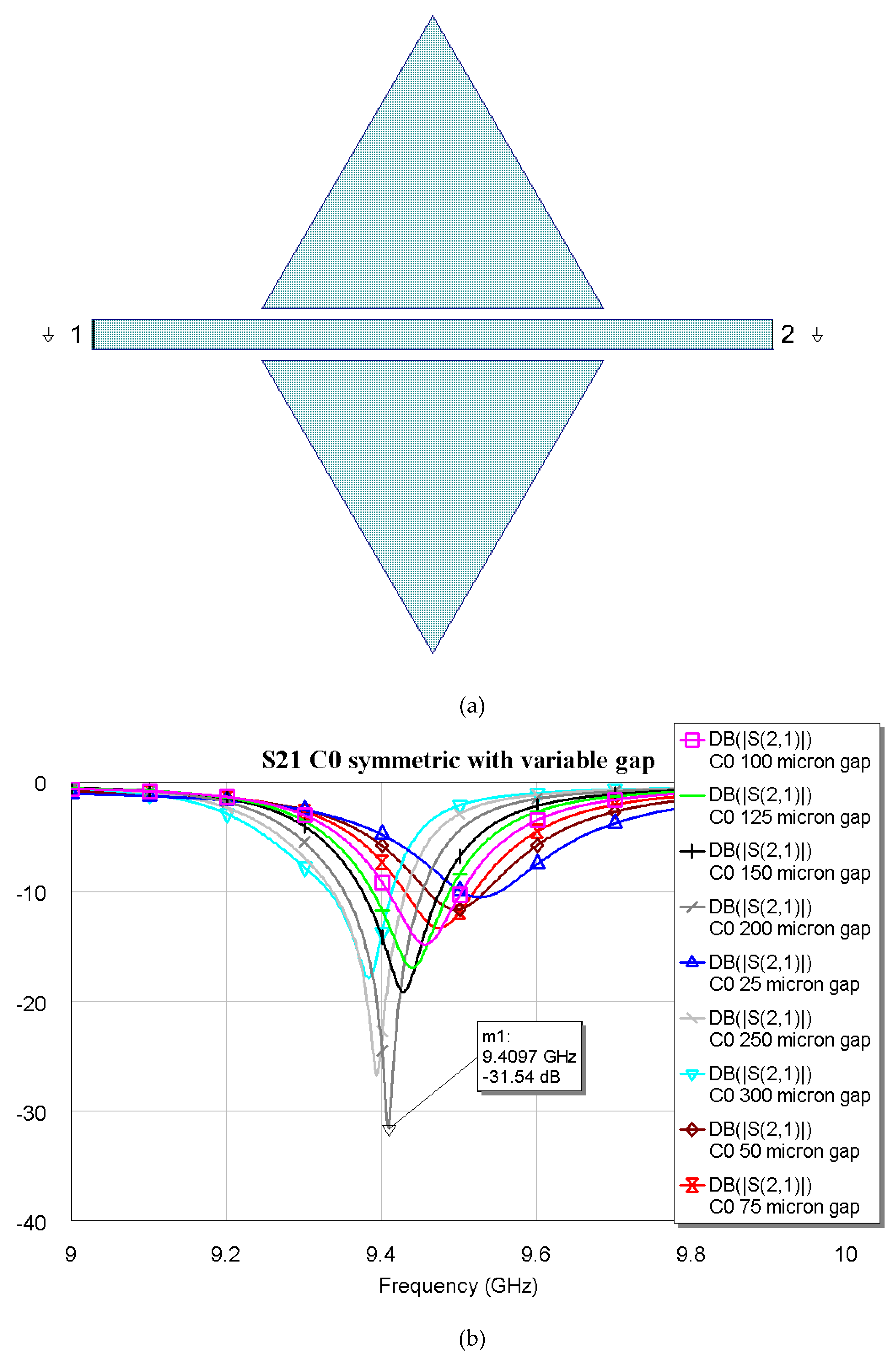
Figure 2.
The transmission coefficient S21 resulting from C0 configuration with variable length was obtained by the electromagnetic simulation of the structures using MWO.
Figure 2.
The transmission coefficient S21 resulting from C0 configuration with variable length was obtained by the electromagnetic simulation of the structures using MWO.
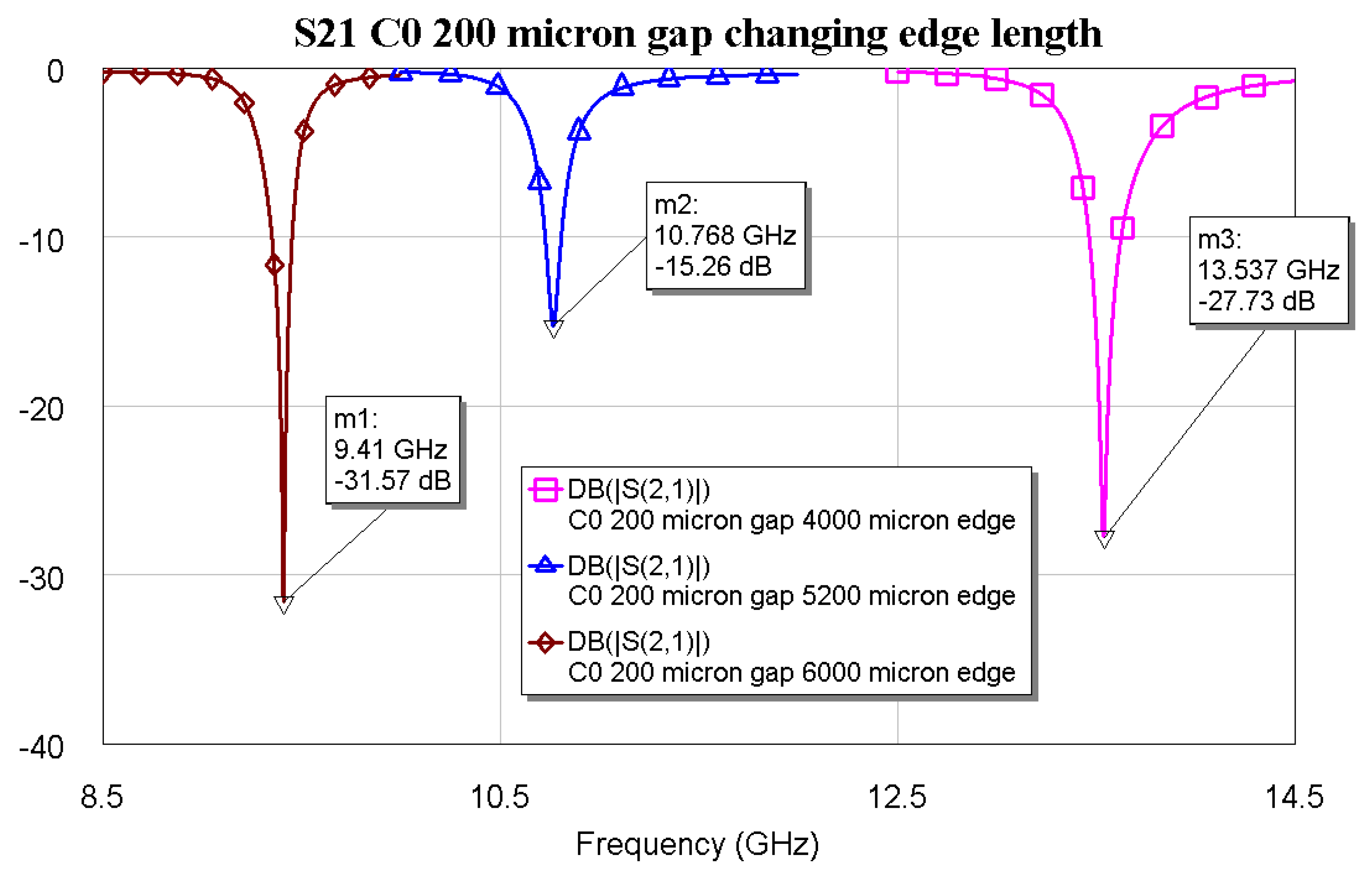
Figure 3.
(a) the resonator layout for C1 configuration; (b) transmission coefficient S21 obtained by the electromagnetic simulation using MWO for different distances between the triangles and microstrip line.
Figure 3.
(a) the resonator layout for C1 configuration; (b) transmission coefficient S21 obtained by the electromagnetic simulation using MWO for different distances between the triangles and microstrip line.
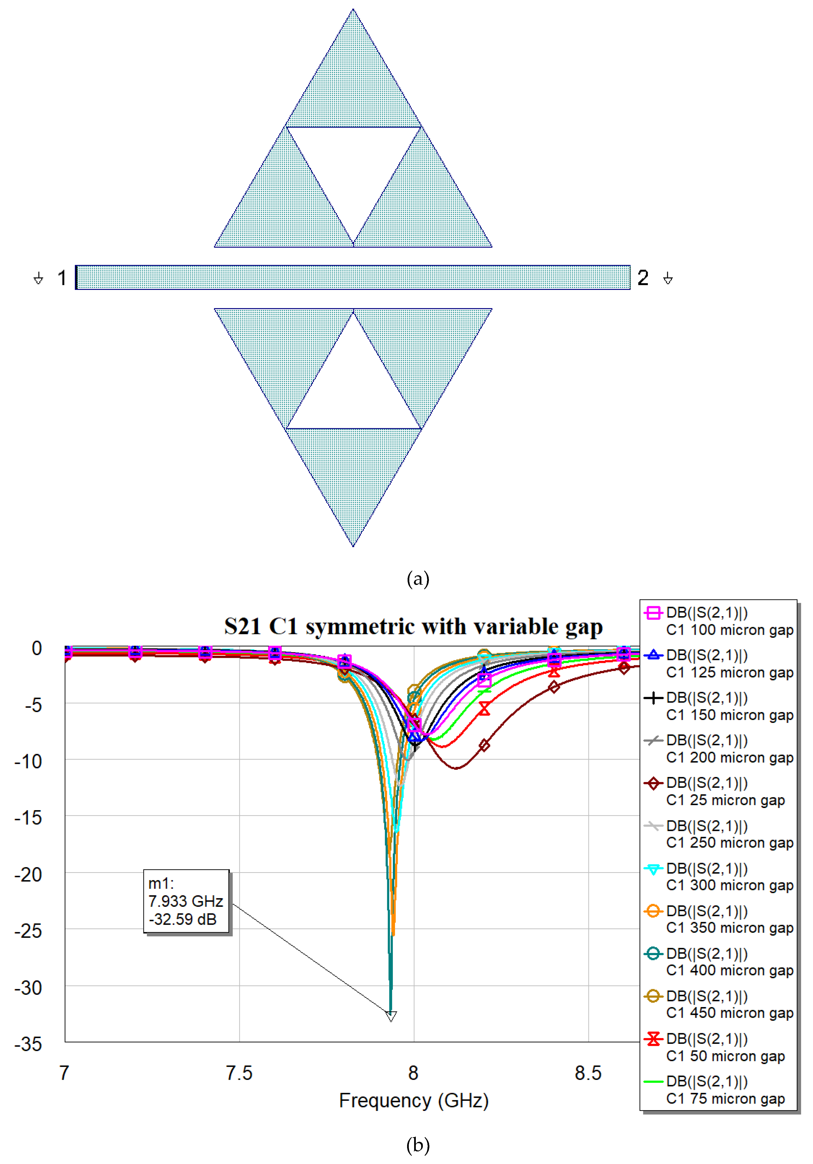
Figure 4.
(a) the resonator layout for C2 configuration; (b) transmission coefficient S21 obtained by the electromagnetic simulation using MWO for different distances between the triangles and microstrip line.
Figure 4.
(a) the resonator layout for C2 configuration; (b) transmission coefficient S21 obtained by the electromagnetic simulation using MWO for different distances between the triangles and microstrip line.
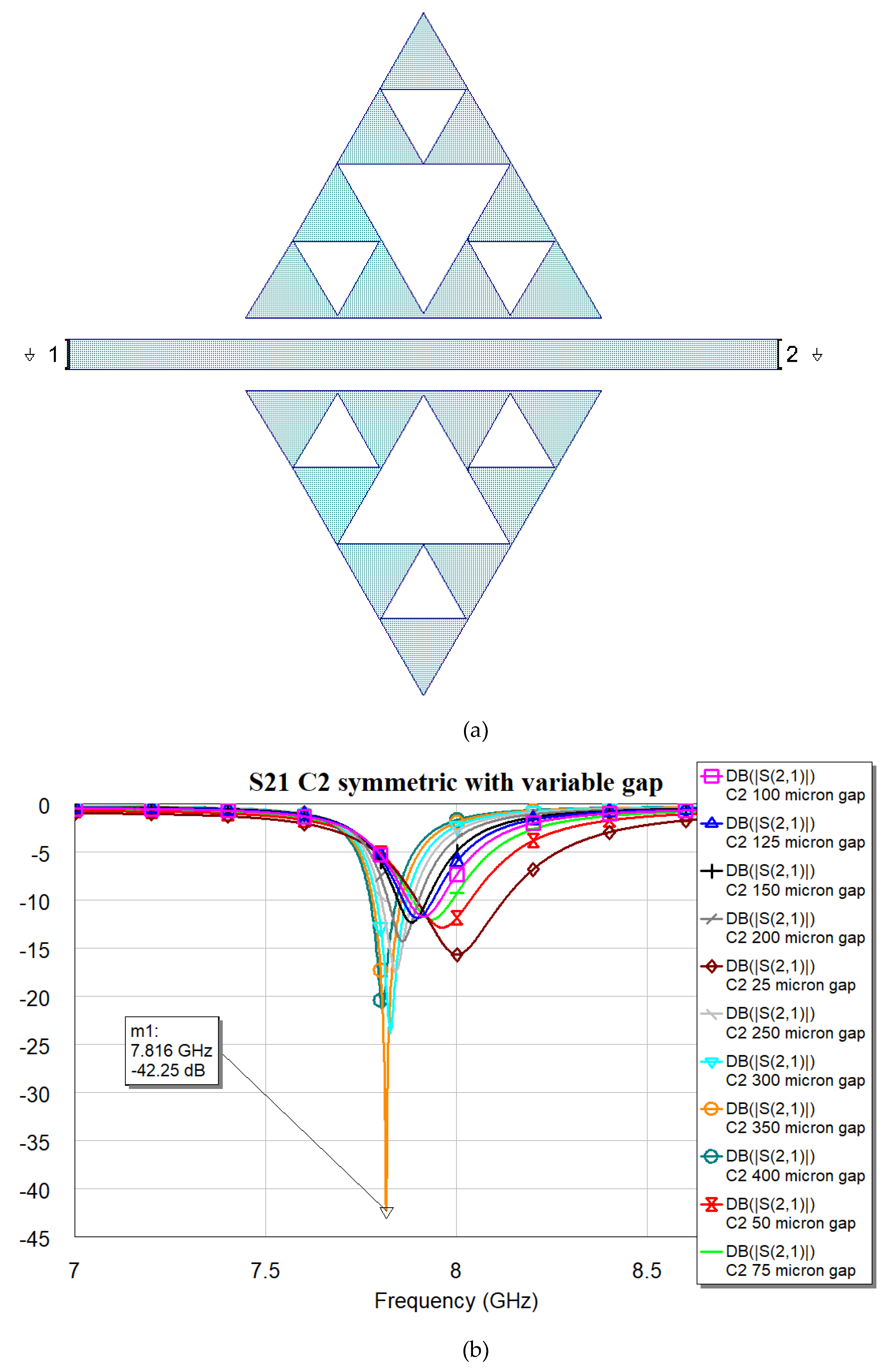
Figure 5.
(a) the resonator layout for C3 configuration; (b) transmission coefficient S21 obtained by the electromagnetic simulation using MWO for different distances between the triangles and microstrip line.
Figure 5.
(a) the resonator layout for C3 configuration; (b) transmission coefficient S21 obtained by the electromagnetic simulation using MWO for different distances between the triangles and microstrip line.
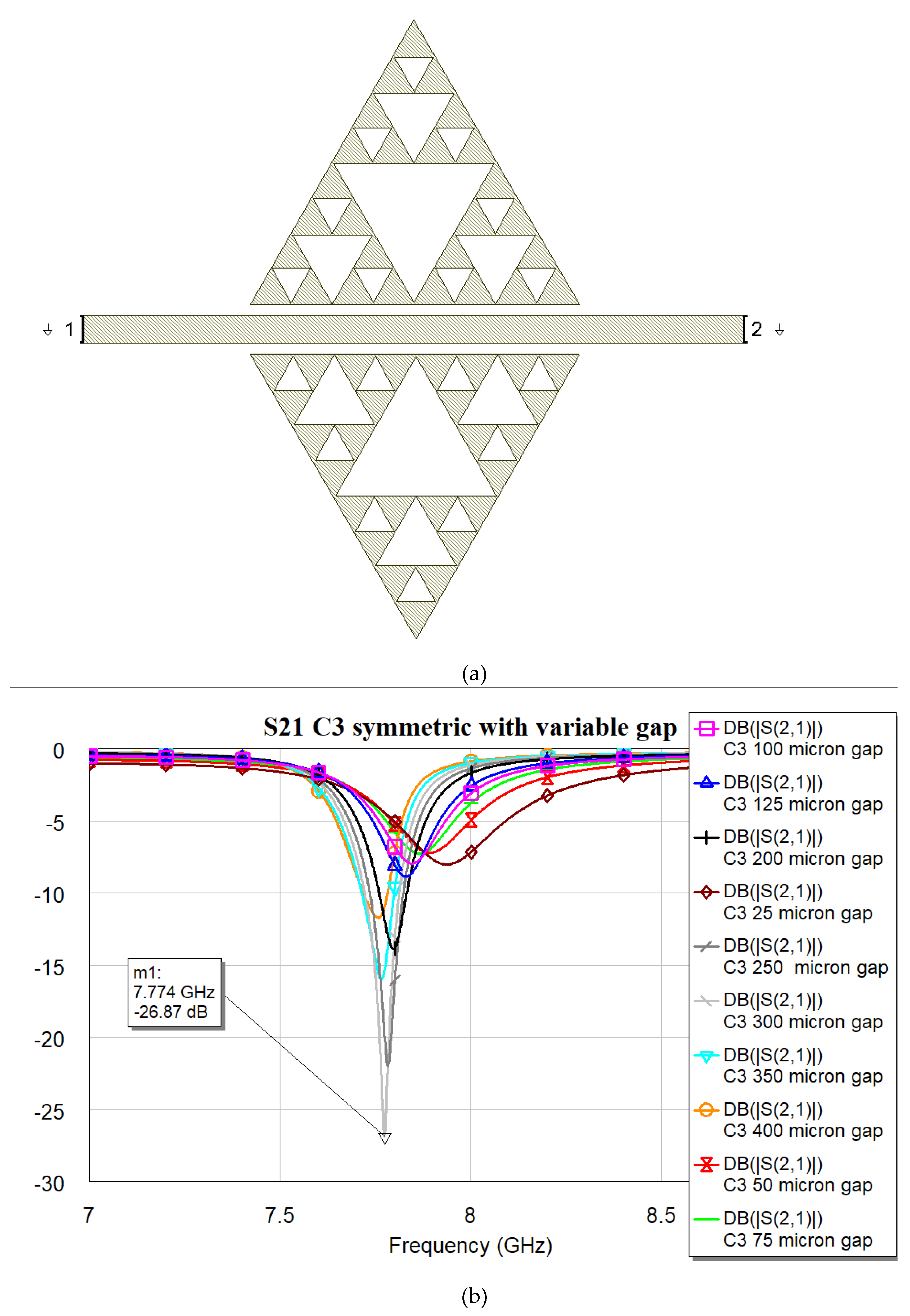
Figure 6.
The transmission coefficient S21 obtained by the electromagnetic simulations for the optimized (abbreviated “opt”) for individual Sierpinski resonators, each with its own separation from the microstrip feeding line.
Figure 6.
The transmission coefficient S21 obtained by the electromagnetic simulations for the optimized (abbreviated “opt”) for individual Sierpinski resonators, each with its own separation from the microstrip feeding line.
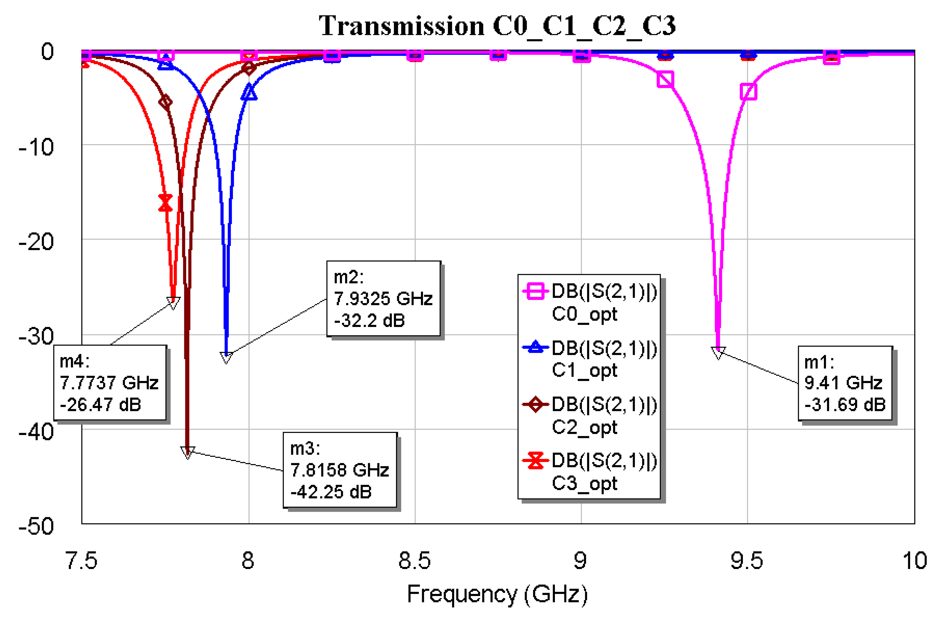
Figure 7.
Electromagnetic simulated resonance frequency response for the optimized individual Sierpinski resonators as a function of the Number of Triangles created inside the single triangle.
Figure 7.
Electromagnetic simulated resonance frequency response for the optimized individual Sierpinski resonators as a function of the Number of Triangles created inside the single triangle.
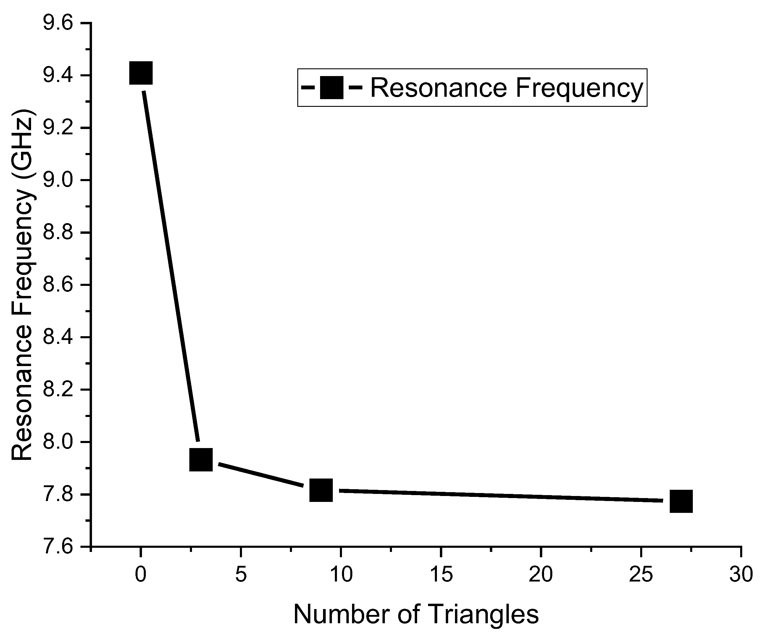
Figure 8.
(a) SPDT Configuration, and (b) Electromagnetic simulation performance (S21=transmission parameter, in dB), S11=reflection, and S32=isolation) for the SPDT switch with the RF MEMS on port 2 actuated, thus providing the passage of the signal on port 2 leaving port 3 isolated. The same performance is obtained when the switch on port 3 is actuated.
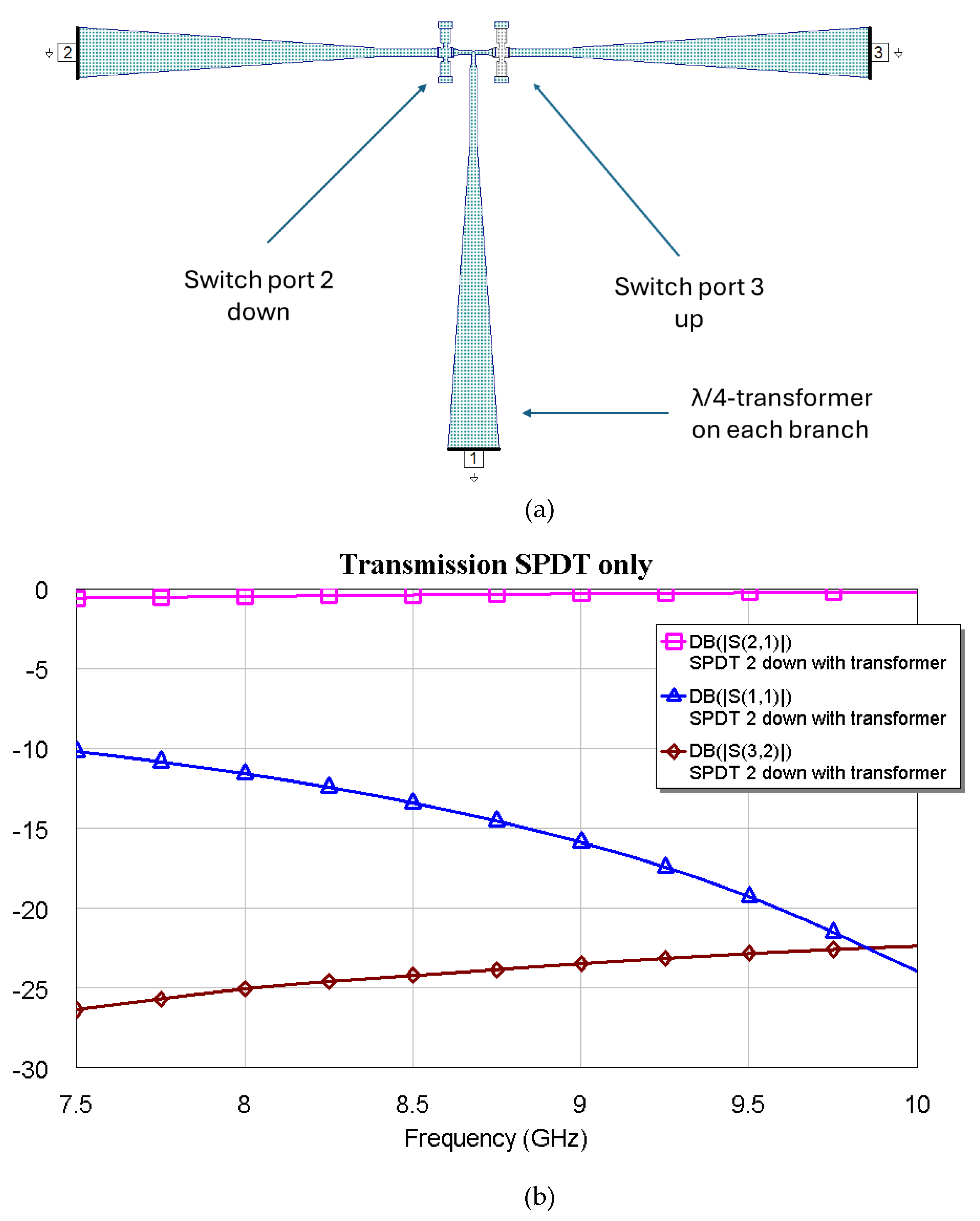
Figure 9.
(a) SPDT connected with C0 and C1, and (b) simulated response for the transmission depending on the actuated branch of the SPDT (2 or 3).
Figure 9.
(a) SPDT connected with C0 and C1, and (b) simulated response for the transmission depending on the actuated branch of the SPDT (2 or 3).
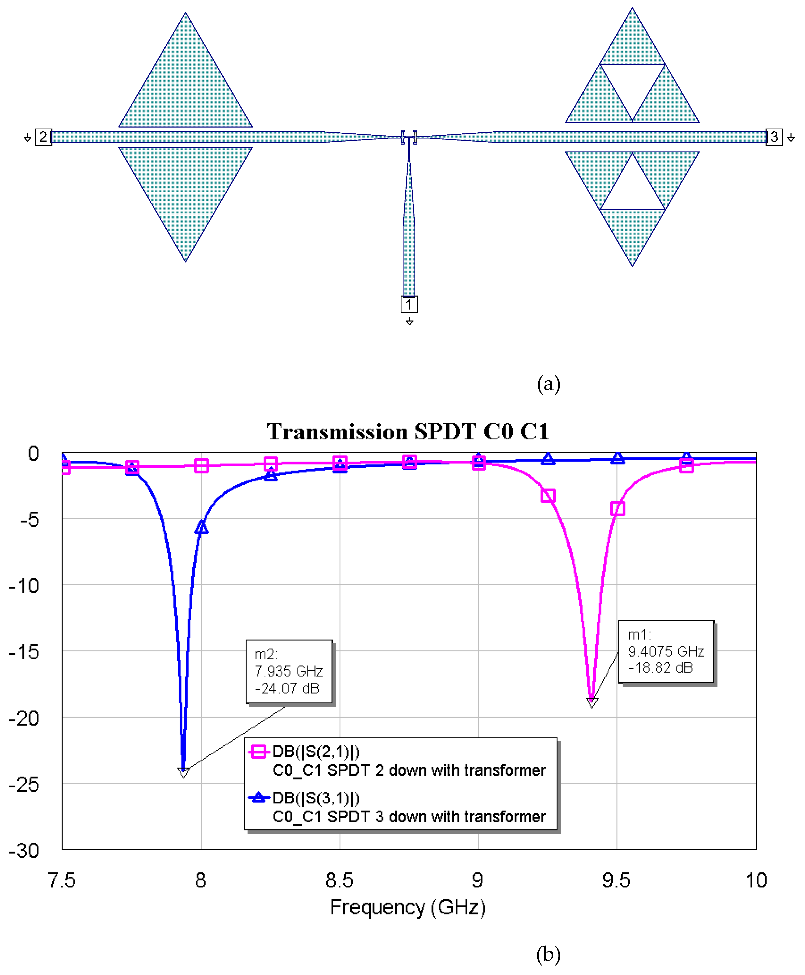
Figure 10.
(a) SPDT connected with C0 and C2, and (b) simulated response for the transmission depending on the actuated branch of the SPDT (2 or 3).
Figure 10.
(a) SPDT connected with C0 and C2, and (b) simulated response for the transmission depending on the actuated branch of the SPDT (2 or 3).
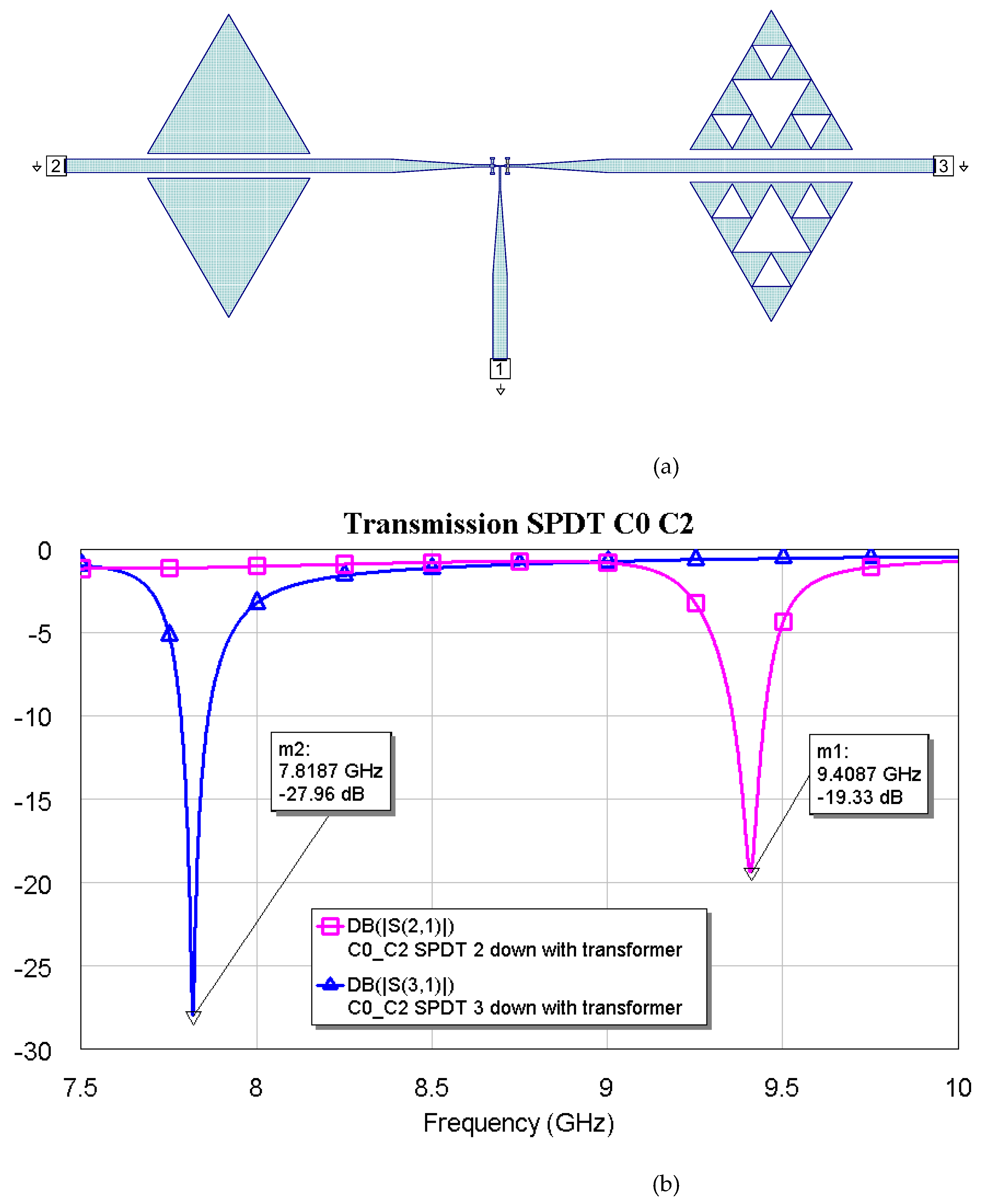
Figure 11.
(a) SPDT connected with C0 and C3, and (b) simulated response for the transmission depending on the actuated branch of the SPDT (2 or 3).
Figure 11.
(a) SPDT connected with C0 and C3, and (b) simulated response for the transmission depending on the actuated branch of the SPDT (2 or 3).
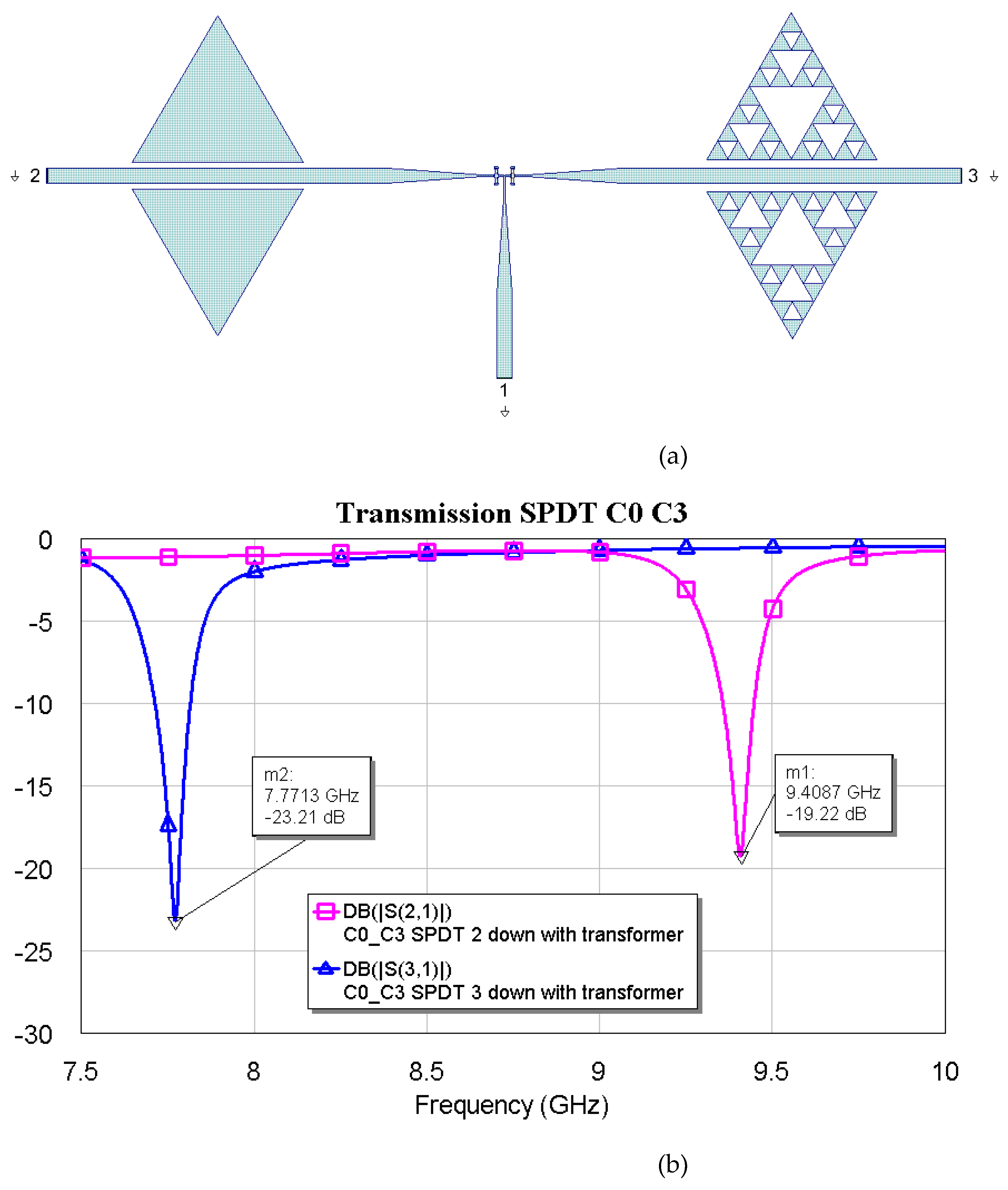
Figure 12.
(a) SPDT connected with C1 and C2, and (b) simulated response in a narrow band for the transmission, depending on the actuated branch of the SPDT (2 or 3).
Figure 12.
(a) SPDT connected with C1 and C2, and (b) simulated response in a narrow band for the transmission, depending on the actuated branch of the SPDT (2 or 3).
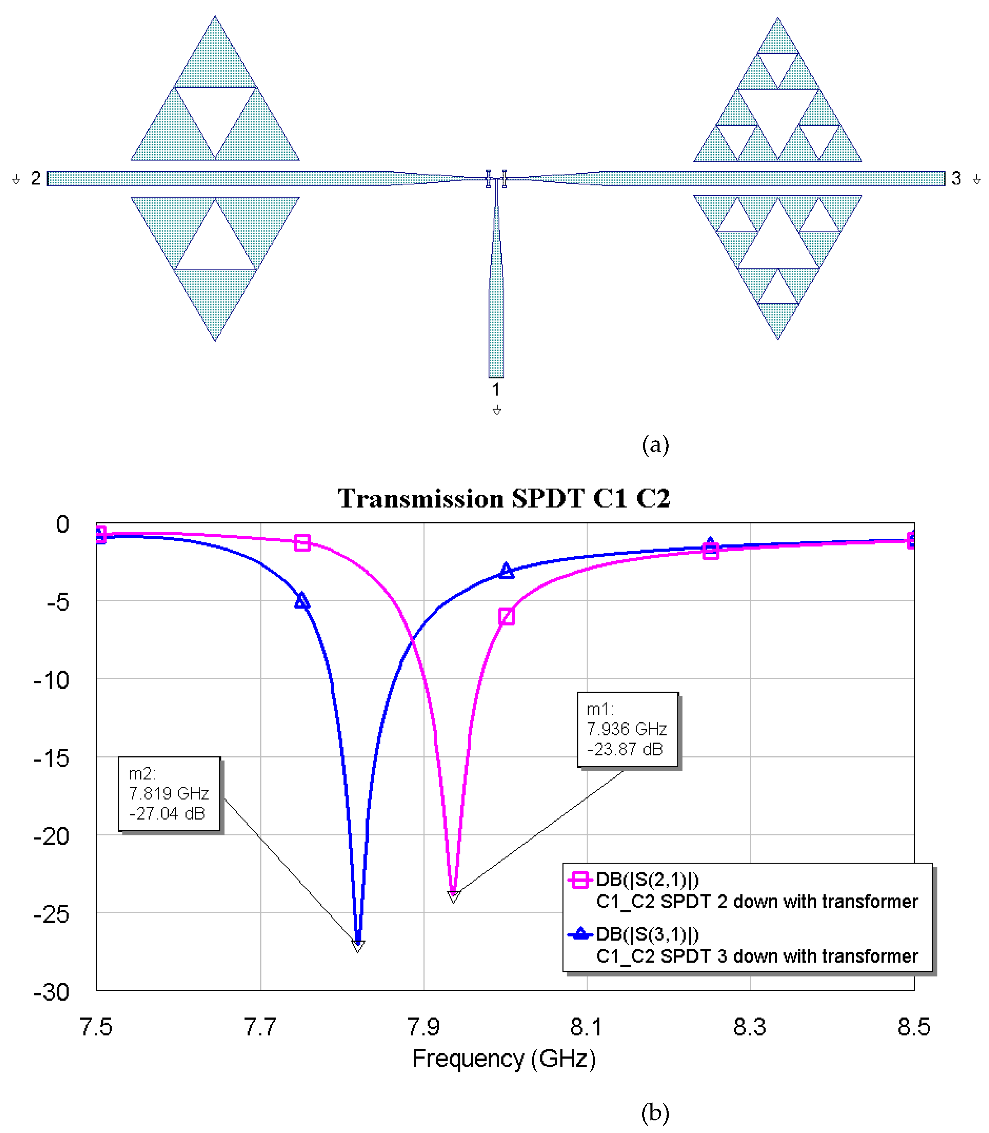
Figure 13.
(a) SPDT connected with C1 and C3, and (b) simulated response in a narrow band for the transmission, depending on the actuated branch of the SPDT (2 or 3).
Figure 13.
(a) SPDT connected with C1 and C3, and (b) simulated response in a narrow band for the transmission, depending on the actuated branch of the SPDT (2 or 3).
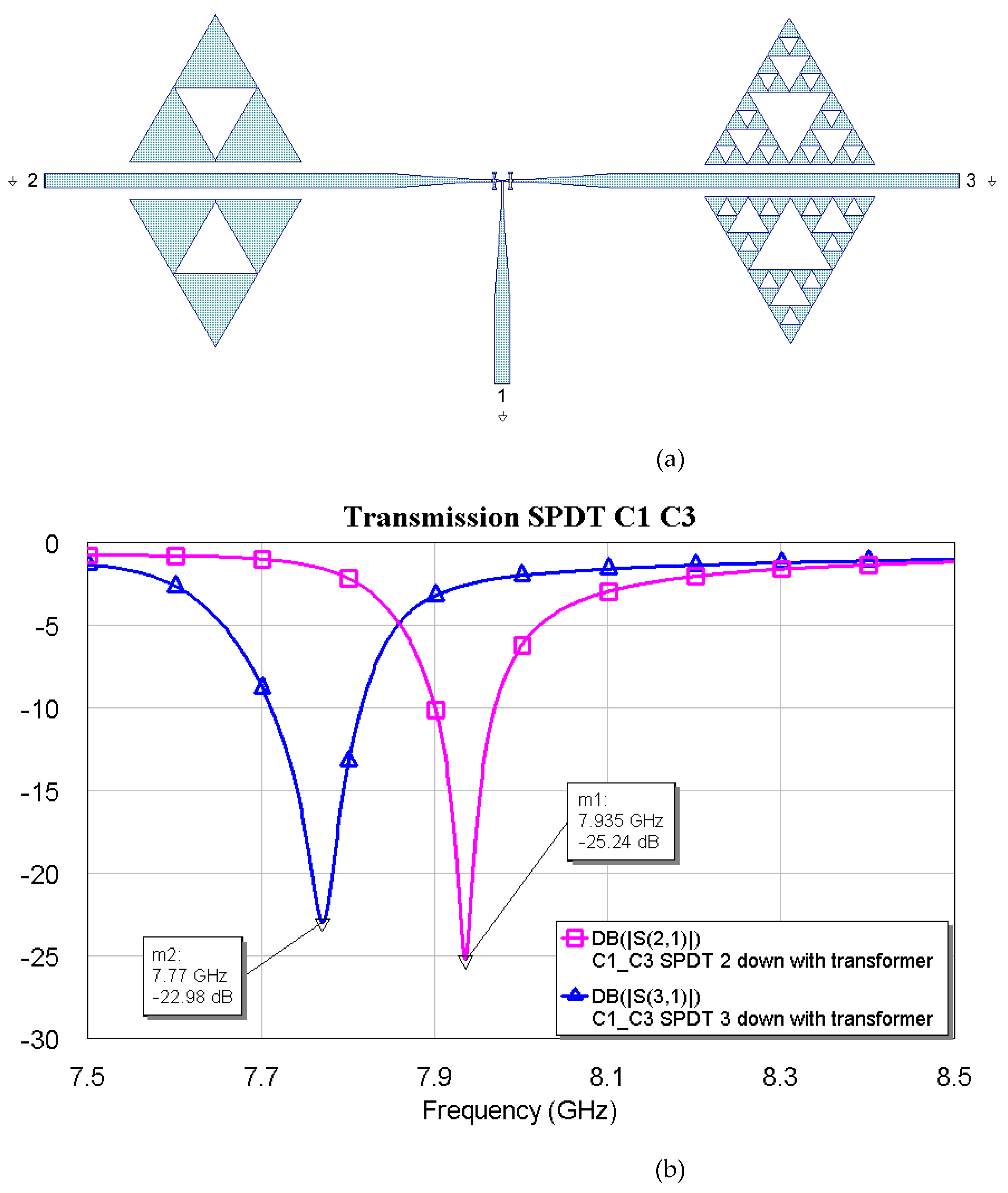
Figure 14.
(a) SPDT is connected with C2 and C3, and (b) a simulated response in a narrow band for transmission, depending on the actuated branch of the SPDT (2 or 3).
Figure 14.
(a) SPDT is connected with C2 and C3, and (b) a simulated response in a narrow band for transmission, depending on the actuated branch of the SPDT (2 or 3).
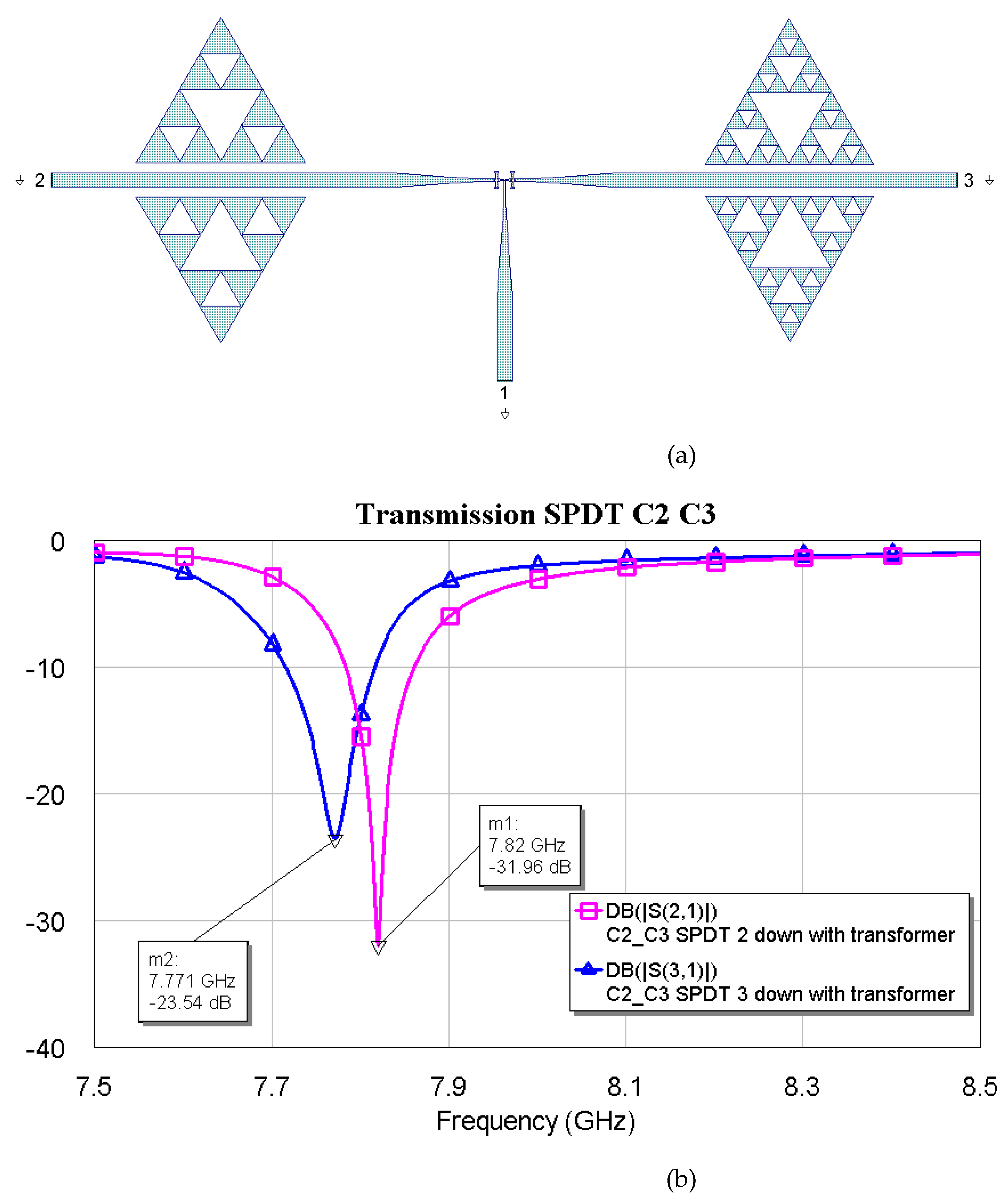

Table 1.
Comparison between the resonance frequencies resulting from the electromagnetic simulation (EM) and those calculated analytically for the configuration C0, using Eq (1).
Table 1.
Comparison between the resonance frequencies resulting from the electromagnetic simulation (EM) and those calculated analytically for the configuration C0, using Eq (1).
| Edge Length (µm) | 6000 | 5200 | 4000 |
|---|---|---|---|
| Fresonance, analytical (GHz) | 9.375 | 10.768 | 13.854 |
| Fresonance,EM (GHz) | 9.410 | 10.768 | 13.537 |
Disclaimer/Publisher’s Note: The statements, opinions and data contained in all publications are solely those of the individual author(s) and contributor(s) and not of MDPI and/or the editor(s). MDPI and/or the editor(s) disclaim responsibility for any injury to people or property resulting from any ideas, methods, instructions or products referred to in the content. |
© 2024 by the authors. Licensee MDPI, Basel, Switzerland. This article is an open access article distributed under the terms and conditions of the Creative Commons Attribution (CC BY) license (http://creativecommons.org/licenses/by/4.0/).
Copyright: This open access article is published under a Creative Commons CC BY 4.0 license, which permit the free download, distribution, and reuse, provided that the author and preprint are cited in any reuse.


