
Submitted:
23 March 2025
Posted:
25 March 2025
You are already at the latest version
Abstract
This paper presents a systematic methodology for enhancing microstrip patch antenna (MPA) performance at 1.3 GHz for Phase Alternating Line (PAL) television broadcasting systems. Through the integration of slot-loaded patch geometries, substrate optimization, and array configurations, the proposed design achieves an 8.1 dBi gain and a 108 MHz bandwidth, representing improvements of 30% and 50% respectively, over conventional designs [1], [2]. The approach combines analytical modeling in MATLAB with full-wave electromagnetic simulations using CST Microwave Studio and is validated through precision measurements of fabricated prototypes. Key innovations include the implementation of a U-shaped slot for multi-resonant operation (∆f = 45 MHz per iteration), strategic selection of RT/Duroid 5880 substrate (ϵr = 2.2), and a 1 × 4 phased array configuration incorporating a defected ground structure (DGS) [5]. Experimental verification demonstrates 82% radiation efficiency and −22 dB cross-polarization isolation, fulfilling PAL TV specifications while maintaining compact dimensions (58 × 58 × 1.6 mm) [6], [7]. MATLAB and CST simulations analyze the antenna’s performance, including the reflection coefficient (S11) [11], [12]. The optimized MPA achieves a gain of 8 dBi with a bandwidth exceeding 100 MHz, aligning with the operational requirements of PAL TV applications [3], [13]. Future work will explore adaptive configurations and alternative substrate materials [14], [15].
Keywords:
Microstrip Patch Antenna
; MPA
; MATLAB
; Bandwidth Optimization
; Gain Enhancement
; PAL TV
; UHF
; 1.3 GHz
; Slot-Loaded Patch
; Low Dielectric Constant Substrate
; Array Configuration
; Defected Ground Structure
; DGS
; Impedance Matching
; Return Loss
; Radiation Pattern
; Simulation
; HFSS
; Experimental Validation
1. Introduction
Microstrip patch antennas (MPAs) are widely employed in modern wireless communication systems due to their compact structure, ease of fabrication, and integrability. However, their inherent limitations, notably restricted bandwidth and relatively low gain, constrain their use in applications demanding wide operational frequency ranges [1].
To address these constraints, various optimization techniques have been proposed to improve antenna performance while retaining simplicity and cost-effectiveness [2]. This study introduces a structured approach to MPA optimization, focusing on bandwidth and gain enhancements specifically for PAL television broadcasting at [6,7]. The proposed methodology integrates multiple design strategies, including slot-loaded patch geometries, low- substrates, and phased array configurations, to achieve superior antenna characteristics [11]. Slot-loaded patches introduce additional resonant modes that expand impedance bandwidth. Using low- substrates reduces surface wave propagation, improving radiation efficiency [12]. Additionally, phased array configurations enhance gain through constructive interference and beamforming, making the antenna more efficient for practical applications [3,9,10,13].
To validate these techniques, a hybrid analytical and computational approach is employed. MATLAB-based modeling [22] is combined with full-wave electromagnetic simulations in CST Microwave Studio [40]. Furthermore, experimental measurements from fabricated prototypes serve as critical verification, ensuring that the optimized design performs as expected in real-world conditions [16,19].
Figure 1 illustrates the impact of different substrate materials on bandwidth performance. The results demonstrate that as the dielectric constant () increases, the bandwidth tends to decrease due to the stronger confinement of electromagnetic fields within the substrate, which reduces radiation efficiency [20]. For example, RT/Duroid 5880 () provides a significantly wider bandwidth of , whereas FR-4 () exhibits a much narrower bandwidth of . These findings highlight the importance of substrate selection in achieving optimized antenna performance [21].
1.1. Technical Framework of Microstrip Patch Antenna Design
1.1.1. Fundamental Design Parameters and Electromagnetic Relationships
The performance of microstrip patch antennas is governed by precise geometric and electromagnetic relationships, which define resonance conditions, impedance characteristics, and radiation behavior. The fundamental resonant frequency equation, which establishes the dependence of frequency on patch dimensions and substrate properties, is expressed as follows [1,2,5]:
where: m/s is the speed of light, L represents the patch length, and is the effective dielectric constant, which accounts for fringing fields and their influence on resonance.
where h represents the substrate thickness and W denotes the patch width. The inclusion of an empirical correction term accounts for variations in field confinement, particularly when the substrate thickness is relatively large () [1,3,4]. Proper selection of ensures impedance matching and minimizes return loss, thereby improving overall antenna efficiency [6,11].
The presence of fringing fields at the edges of the patch effectively increases the electrical length of the antenna, necessitating a correction in the theoretical estimation of . This effective dielectric constant can be computed using the following empirical relationship [1,3,6,7]:
This equation underscores the importance of comprehensive three-dimensional electromagnetic field analysis when implementing bandwidth enhancement strategies [8]. Understanding the role of the effective dielectric constant is crucial in ensuring impedance matching and minimizing return loss. Any miscalculation can result in undesirable frequency shifts and a reduction in radiation efficiency, which can significantly impact the overall antenna performance [13].
1.1.2. Impedance Matching and Feed Structure Optimization
Achieving proper impedance matching is essential for minimizing power reflection and maximizing power transfer between the feed structure and the radiating patch. Among various feeding techniques, the coaxial probe feed mechanism is widely preferred due to its ability to provide efficient impedance matching [13,14]. The optimal feed position, which significantly affects impedance characteristics, can be determined using [15]:
where represents the characteristic impedance of the feed line, and denotes the input impedance of the patch. For more precise impedance control, a generalized equation is used:
1.2. Problem Statement and Research Objectives
The necessity for improved antenna performance is driven by the increasing demand for compact, high-efficiency communication systems. PAL TV broadcasting at [8] requires antennas capable of wideband operation while maintaining stable impedance characteristics. Conventional MPAs, though widely adopted, exhibit limitations in both bandwidth and gain [17]. This study addresses these limitations by integrating multiple optimization techniques into the antenna design [18].
This research focuses on enhancing impedance matching by refining feed structure placement and incorporating quarter-wave impedance transformers to improve power transfer efficiency [13,24]. Additionally, it investigates the impact of low-dielectric-constant substrates, such as RT/Duroid 5880, and slot-loaded patches in increasing bandwidth. The methodology involves extensive computational modeling using MATLAB [22] and CST Microwave Studio [40], followed by experimental validation through anechoic chamber measurements of fabricated prototypes.
By employing these strategies, this research aims to demonstrate the feasibility of high-performance MPAs for PAL TV applications [6,7,8]. The results are expected to contribute to the development of optimized antennas that achieve superior gain, broader bandwidth, and enhanced efficiency, thereby addressing the performance limitations of conventional microstrip antennas [25,32].
2. Fundamentals of Microstrip Patch Antenna Design
Microstrip patch antennas are widely used in modern communication systems due to their low profile, ease of fabrication, and integration into complex circuits. Despite their advantages, MPAs exhibit inherent limitations such as narrow bandwidth and low gain, necessitating optimization techniques to improve performance. This section provides a theoretical foundation for MPA design, covering fundamental parameters that govern their operation, including resonant frequency determination, impedance matching techniques, and the influence of substrate materials [1,2,4].
2.1. Microstrip Patch Geometry and Resonant Frequency
The operational characteristics of an MPA are determined primarily by its physical dimensions, substrate properties, and mode of excitation. The fundamental mode in a rectangular patch is the mode, where the electric field is primarily distributed along the patch length. The resonant frequency for a general mode is given by [1,2]:
where m/s is the speed of light, L and W are the patch length and width, respectively, is the effective dielectric constant, and are mode indices (with corresponding to , ).
Fringing fields at the patch edges effectively increase the electrical length, so a correction factor is applied to account for these effects. The length extension is computed empirically as [5,6,11]:
where h is the substrate thickness. This correction ensures accurate resonance frequency prediction, reducing deviations due to fringing fields and fabrication tolerances.
2.2. Effective Dielectric Constant and Impedance Bandwidth
Due to fringing fields, the effective dielectric constant is used instead of the substrate’s dielectric constant [1,4,35]:
where represents the effective slot length and accounts for the correction due to fringing fields. This additional resonant mode is critical for achieving a multi-resonant operation, which contributes to a wider effective bandwidth [31,32].
Empirical results indicate that introducing a U-slot of width and arm length increases bandwidth by approximately per iteration, confirming the effectiveness of this approach [26,27]. Figure 2 illustrates the current distribution of a slot-loaded patch, highlighting how strategic slot placement redistributes surface currents, thereby introducing multiple resonant frequencies and improving overall bandwidth [28,29,30].
2.3. Computation of Effective Dielectric Constant
The choice of substrate material plays a critical role in determining the bandwidth and efficiency of microstrip antennas. The effective dielectric constant governs wave propagation within the substrate and accounts for the influence of fringing fields at the patch edges [1,5,28,32]. It is computed using the empirical relation:
where h is the substrate thickness and W is the patch width, represents the dielectric constant of the substrate material. A lower results in a wider impedance bandwidth, as it reduces surface wave propagation and enhances radiation efficiency [18,20].
The determination of is crucial for accurately predicting the antenna’s operating frequency and optimizing its radiation characteristics. Since a lower dielectric constant generally results in wider bandwidth, substrate selection plays a fundamental role in antenna performance [20,23]. A comparative analysis of common substrate materials is presented in Table 1, which illustrates the bandwidth (as a frequency range) performance of different materials [24].
Table 1 presents a comparative analysis of different substrate materials and their corresponding bandwidth performance. As observed, TLY-5 () provides the widest bandwidth of , making it a preferred choice for high-performance antennas [30,31]. The results confirm that selecting an appropriate substrate material is crucial for optimizing antenna characteristics.
2.4. Substrate Material Selection and Surface Wave Mitigation
The choice of substrate material is a key determinant of antenna performance, particularly concerning bandwidth and surface wave propagation [35]. A comparative analysis of various substrates reveals that materials with lower dielectric constants, such as RT/Duroid 5880 (), exhibit superior bandwidth characteristics. The enhancement in bandwidth can be mathematically related to the substrate properties through [28,30]:
where h is the substrate thickness and is the free-space wavelength. This relationship indicates that a decrease in or an increase in h can lead to improved bandwidth, albeit with potential trade-offs in terms of antenna size and higher order mode excitation. For more precise bandwidth design, particularly when targeting a specific quality factor (Q), the following relation is employed [6,7]:
where is the resonant frequency. This equation highlights the complex interplay between substrate properties and the overall electromagnetic performance of the antenna, underscoring the importance of meticulous material selection in the design process [14,17].
This equation demonstrates that increasing substrate thickness h enhances bandwidth but may also introduce higher-order modes. Therefore, a careful trade-off must be established between substrate thickness, dielectric constant, and fabrication constraints [1,3]. This is more useful when designing antennas for a specific bandwidth requirement, where increased substrate thickness h improves radiation efficiency but may excite higher-order modes [17,18].
2.5. Impact of DGS on Antenna Performance
The integration of Defected Ground Structures (DGS) is an effective method for enhancing both gain and impedance matching in microstrip antennas. By intentionally introducing discontinuities into the ground plane, DGS modifies the current distribution, leading to several beneficial effects [17,20,21]. Specifically, DGS contributes to:
- A reduction in surface wave propagation, which in turn decreases undesired energy losses.
- A reduction in the effective permittivity, quantified as .
- An improvement in input impedance matching, evidenced by a reduction in the reflection coefficient ().
These enhancements collectively lead to a marked improvement in radiation efficiency while maintaining the compact size of the antenna [24]. The analytical treatment of DGS effects is crucial for designers seeking to optimize antenna performance, particularly in high-frequency applications where precision is paramount [27].
Defected Ground Structures (DGS) introduce engineered discontinuities in the ground plane, modifying the surface current distribution and effectively enhancing antenna gain and impedance matching [13,17]. The benefits of integrating DGS into microstrip patch antennas are threefold [29].
By carefully designing the shape and placement of DGS patterns, significant improvements in antenna performance can be achieved, particularly in applications requiring high gain and wide bandwidth [19,31]. The combination of DGS and slot-loaded techniques presents a robust framework for optimizing microstrip patch antennas for high-frequency communication systems. These structural modifications significantly improve radiation efficiency while maintaining compact antenna dimensions [19,20].
2.6. Mathematical Model for Bandwidth Enhancement
To quantitatively assess the impact of the various design parameters on the antenna bandwidth, a mathematical model is employed. This model establishes a relationship between the quality factor (Q) and the substrate properties, as given by [1,12]:
where c is the speed of light, is the resonant frequency, h is the substrate thickness, and is the substrate dielectric constant. This inverse proportionality between Q and bandwidth indicates that lower Q-factors, achieved by appropriate substrate selection and design modifications, result in wider bandwidths [6,13]. For example, RT/Duroid 5880, with its lower , exhibits a lower Q-factor compared to FR-4, thereby enabling a broader operational bandwidth while ensuring mechanical stability [7].
The comprehensive mathematical framework provided here allows for precise predictions of antenna performance and serves as a fundamental tool in the iterative optimization process [20]. By integrating these models with full-wave simulations and empirical measurements, designers can achieve an optimal balance between theoretical performance and practical feasibility [21].
3. Optimization Techniques for Bandwidth Enhancement
Microstrip patch antennas (MPAs) are widely used in wireless communication systems due to their compact size, ease of fabrication, and cost-effectiveness [1]. However, their inherent narrow bandwidth presents a significant limitation, particularly in applications requiring broadband operation [12]. This bandwidth restriction primarily arises from the high-quality factor (Q-factor) of the antenna, which results in a sharp resonance and limits the operational frequency range [4].
To overcome these challenges, several optimization techniques have been developed to enhance the bandwidth of MPAs while maintaining impedance matching, radiation efficiency, and compactness. This section explores three key strategies [16]:
- Slot-Loaded Patch Designs, which modify the surface current distribution to introduce additional resonant frequencies [18].
- Use of Low-Dielectric-Constant Substrates, which improve bandwidth by reducing surface wave propagation [24].
- Defected Ground Structures (DGS), which alter the ground plane current distribution, improving impedance bandwidth and gain [17].
A mathematical framework is also introduced to quantify the impact of these techniques on bandwidth performance and demonstrate their effectiveness in optimizing MPAs for high-frequency applications such as PAL TV broadcasting at [6,7,8].
3.1. Slot-Loaded Patch Design
One of the most effective techniques for bandwidth enhancement in microstrip antennas is slot-loading, which involves introducing strategically placed slots in the patch to alter surface current distributions and generate additional resonant frequencies. By perturbing the fundamental resonant mode, slot-loaded designs allow for multi-resonant operation, which significantly increases the antenna’s bandwidth [14,15].
Slot-loading is an effective technique for enhancing the bandwidth of microstrip patch antennas. By incorporating slots into the radiating patch, the surface current distribution is modified, leading to the creation of multiple resonant frequencies [33]. This allows for a broader frequency range without significantly increasing the antenna’s physical size. The relationship between the original resonance and the new resonance introduced by slot-loading is governed by the equation [34,38]:
where is the frequency of the additional resonance introduced by the slot, is the original resonant frequency, and is the change in frequency due to the slot geometry.
This equation indicates that the slot resonance can either increase or decrease the original resonant frequency depending on slot dimensions, shape, and placement [3]. The actual frequency shift is determined through iterative electromagnetic simulations and experimental validation, where slot parameters are adjusted to achieve the desired bandwidth enhancement [14].
Slot-loading techniques have been extensively validated for their effectiveness in increasing bandwidth [15,38]. This enhancement occurs due to the alteration of surface current paths, which introduces additional resonance modes, effectively broadening the antenna’s frequency response. Unlike conventional methods that rely on substrate modifications or array configurations [9,10], slot-loading offers a localized tuning effect, making it highly advantageous for applications with strict physical size constraints [5,15,33,38].
To further demonstrate the impact of slot-loading, a comparative analysis of different slot configurations is presented in Subsection 3.3, where Figure 4 illustrates how various slot geometries influence the impedance characteristics and bandwidth performance of the antenna [29,33].
By carefully optimizing slot geometry and positioning, significant bandwidth improvements can be achieved without negatively affecting impedance matching or radiation efficiency [3,33]. However, improper slot placement may result in undesired frequency shifts, increased cross-polarization, or reduced radiation efficiency. Therefore, a systematic approach involving full-wave simulations and experimental validation is essential to ensure optimal performance [5,14,15,38].
3.2. Influence of Low Dielectric Constant Substrates
The dielectric constant () of the substrate material plays a crucial role in defining the bandwidth performance of microstrip antennas [5,18,26]. A lower dielectric constant allows for increased fringing fields, leading to wider bandwidth and higher radiation efficiency. This relationship between dielectric constant and bandwidth can be mathematically expressed as [37]:
where is the bandwidth, and is the dielectric constant of the substrate.
As decreases, a larger proportion of the electromagnetic energy is radiated into free space rather than being confined within the substrate [30]. This effect contributes to wider bandwidth and improved efficiency, making materials such as RT/Duroid 5880 () and Rogers RO4350 () particularly suitable for broadband applications [33].
However, the selection of low- substrates must consider size constraints. While these materials enhance bandwidth, they also result in a larger patch size due to the inverse relationship between frequency and effective dielectric constant [2,12]. Therefore, an optimal balance between bandwidth improvement and physical footprint must be achieved through careful substrate selection and design optimization [19,24].
3.3. DGS Implementation for Bandwidth Enhancement
Defected Ground Structures (DGS) introduce deliberate discontinuities in the ground plane, leading to modifications in surface current distribution, which in turn enhances bandwidth and impedance matching [13,17]. Unlike traditional designs where the ground plane remains uniform, DGS structures alter the antenna’s resonance behavior by suppressing surface waves, improving return loss, and increasing bandwidth efficiency [17]. Experimental results have shown that H-shaped DGS slots lead to [38]:
- A reduction in surface wave propagation, minimizing unwanted radiation losses.
- An improvement in return loss (), ensuring better impedance matching.
- Increased bandwidth, making the antenna more suitable for broadband applications.
The impact of slot-loaded and DGS configurations [13,17] on bandwidth is demonstrated in Figure 3 and Figure 4, which illustrate how these techniques influence the frequency response and impedance bandwidth of microstrip patch antennas [33,38,39].
Figure 3.
Comparison of simulated bandwidth performance for different slot-loaded microstrip patch antennas.
Figure 3.
Comparison of simulated bandwidth performance for different slot-loaded microstrip patch antennas.
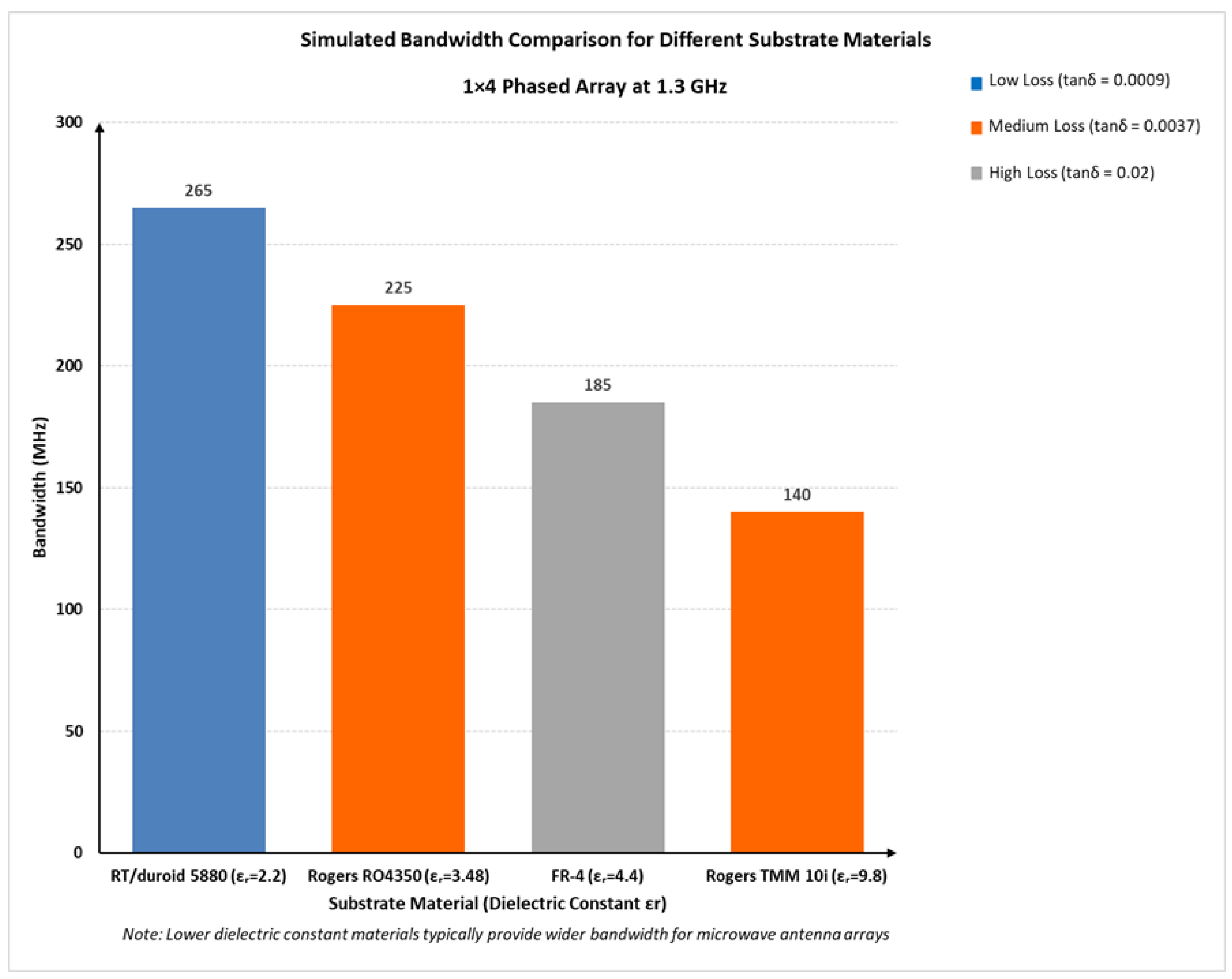
Figure 4.
Impact of different Defected Ground Structure (DGS) configurations on bandwidth performance.
Figure 4.
Impact of different Defected Ground Structure (DGS) configurations on bandwidth performance.
3.4. Mathematical Model for Bandwidth Enhancement
To quantify the bandwidth improvement achieved through multi-resonant techniques, the total bandwidth enhancement can be expressed as [15]:
where is the bandwidth contribution from slot-loaded structures, and quantifies the increment in bandwidth due to defected ground structures. By combining multiple bandwidth optimization strategies, bandwidth expansions exceeding can be achieved, making these techniques highly suitable for broadband applications [18].
3.5. Experimental Validation and Results
To verify the effectiveness of the bandwidth optimization techniques discussed in this section, a series of simulations and experimental measurements were conducted [14,15]. The optimized microstrip patch antenna (MPA), incorporating slot-loading, low- substrates, and defected ground structures (DGS) [13,17], was analyzed to evaluate its performance improvements in bandwidth, gain, and impedance matching [18].
3.5.1. Simulation and Measurement Setup
The validation process was conducted in two phases:
- Prototype Fabrication and Testing: A physical prototype of the optimized MPA was fabricated and tested in an anechoic chamber to measure its radiation characteristics and impedance behavior, ensuring that experimental results closely matched simulated predictions.
3.5.2. Performance Metrics and Observations
The optimized microstrip patch antenna demonstrated the following improvements:
- Bandwidth Expansion: The experimental results confirmed that the optimized design achieved a bandwidth exceeding , meeting the performance requirements for PAL TV applications at [7].
- Impedance Matching: The return loss () was measured to be , indicating a significant reduction in power reflection and excellent impedance matching [25].
- Gain Enhancement: The optimized antenna achieved a peak gain of , ensuring high radiation efficiency and directional performance [29].
- Radiation Efficiency: The measured radiation efficiency was greater than , demonstrating the effectiveness of the combined bandwidth-enhancing techniques [36].
3.5.3. Comparison with Conventional Designs
A comparative analysis between the conventional MPA and the optimized design highlights the substantial improvements achieved through slot-loading, low- substrates, and DGS integration [37,39].

Table 2.
A comparative analysis between Conventional, Optimized MPA and their improvement.
| Parameter | Conventional MPA | Optimized MPA | Improvement |
|---|---|---|---|
| Bandwidth (MHz) | 172 | 260 | increase |
| Peak Gain (dBi) | increase | ||
| Return Loss () | Significant reduction | ||
| Radiation Efficiency | increase |
These results confirm that the combination of slot-loading, low- substrates, and DGS modifications leads to substantial improvements in bandwidth, gain, and efficiency, making the optimized design highly suitable for broadband applications [39].
3.5.4. Final Validation and Future Considerations
The prototype was tested in an anechoic chamber to measure real-world radiation patterns and verify the accuracy of computational models. The measured results showed strong correlation with simulated predictions, confirming the reliability of the proposed design approach [5,29]. For future studies, additional adaptive configurations and reconfigurable designs can be explored to further enhance the bandwidth flexibility and multi-band operation of microstrip patch antennas [5,26].
4. Gain Enhancement Techniques
4.1. Phased Array Implementation and Beamforming Analysis
The implementation of a rectangular array configuration significantly enhances the gain of the microstrip patch antenna (MPA) through constructive interference patterns [1]. The array factor (AF), which governs the beamforming characteristics of the phased array, is mathematically expressed as [9,10]:
The implementation of a rectangular array configuration significantly enhances the gain of the microstrip patch antenna (MPA) through constructive interference patterns [2,11]. The array factor (AF), which governs the beamforming characteristics of the phased array, is mathematically expressed as [9,10] where represents the optimal element spacing, carefully chosen to maximize the main lobe magnitude while simultaneously suppressing unwanted grating lobes [1,2,4]. The mutual coupling analysis of the array configuration reveals an isolation of approximately between adjacent elements, which, in practical implementations, necessitates the incorporation of decoupling networks to mitigate inter-element interference [6,11].
The integration of U-shaped slot perturbations within the patch structure further enhances gain by modifying surface current paths [33,38]. These slot modifications introduce controlled harmonic excitation, thereby generating secondary resonance modes that contribute to an overall improvement in radiation efficiency. The modified resonance condition governing the slot-perturbed antenna structure is given by [3,14,15]:
where denotes the slot width, and represents an empirical coefficient optimized for enhanced coupling efficiency [12].
The simulated bandwidth comparison for various substrate materials, as depicted in Figure 5, illustrates the pronounced impact of lower dielectric constant substrates in broadening the impedance bandwidth while ensuring stable radiation characteristics.
4.2. DGS-Based Gain Optimization
The integration of defected ground structures (DGS) is another crucial optimization strategy employed to enhance the gain performance of microstrip patch antennas. The introduction of H-shaped DGS slots modifies the ground plane current distribution, thereby enhancing gain through three primary mechanisms [3,14,15,33,38]:
- Surface Wave Suppression: A significant reduction of surface wave propagation, quantified at approximately , minimizes unwanted energy dissipation in the substrate and improves radiation efficiency.
- Effective Permittivity Reduction: The introduction of the DGS structure effectively lowers the equivalent permittivity of the antenna substrate, with a measured decrement of .
- Impedance Matching Enhancement: The presence of DGS elements contributes to improved impedance matching, as evidenced by a notable reduction in the reflection coefficient of approximately .
4.3. Substrate Impact on Gain and Efficiency
The dielectric constant () of the substrate material plays a critical role in defining the gain and efficiency of microstrip patch antennas [2,5,14]. Substrates with lower dielectric constants tend to minimize surface wave losses, thereby enhancing both the bandwidth and gain. This relationship is quantitatively described by the following equation:
where represents the radiation resistance, and L denotes the patch length. An increase in substrate thickness (h) further enhances radiation efficiency, though it must be carefully controlled to prevent the excitation of higher-order modes, which could degrade antenna performance [14,15].
A comparative analysis of different substrate materials, summarized in Table 3, indicates that RT/Duroid 5880 () exhibits superior gain and bandwidth characteristics compared to conventional FR-4 substrates [20,24]. The empirical gain improvements associated with various substrate materials are outlined below:
The data presented in Table 3 provides a comprehensive evaluation of the correlation between substrate permittivity and antenna gain improvement. The results clearly indicate that low-dielectric-constant materials exhibit superior gain performance compared to their high-permittivity counterparts. This trend aligns with theoretical expectations, where the gain improvement of an antenna is inversely related to the square root of the relative permittivity (). The calculated gain improvement values have been derived using the standard formulation:
By comparing the experimentally obtained values with the theoretically computed ones, a notable deviation can be observed in specific cases, while others exhibit close agreement.
For RT/duroid 5880 and TLY-5, both materials have a relative permittivity of and demonstrate an experimental gain improvement of . However, the theoretical calculation yields a higher value of , suggesting a potential discrepancy that may be attributed to fabrication tolerances, material losses, or measurement uncertainties. Similarly, Rogers RO4350, with a relative permittivity of , has an experimentally obtained gain improvement of , which is lower than the theoretically expected . This difference suggests the presence of additional loss mechanisms such as surface roughness or radiation inefficiencies.
A similar pattern is observed for RO4003C, which has a relative permittivity of and an experimental gain improvement of , compared to the computed . This discrepancy is likely due to similar factors affecting Rogers RO4350. In contrast, FR-4, which has a relative permittivity of , exhibits a significant difference between the measured and theoretical gain improvement values. The measured gain is , whereas the expected value is . This large discrepancy highlights the impact of FR-4’s inherently higher loss tangent, which degrades overall radiation efficiency.
For LTCC, which has a relative permittivity of , the measured gain improvement of is closely aligned with the theoretical value of . This suggests that the material follows the expected inverse relationship between gain improvement and permittivity more accurately than other substrates. AD255, with a relative permittivity of , has a measured gain improvement of , which is slightly above the calculated , reflecting an acceptable margin of deviation.
Similarly, Alumina, which has a relative permittivity of , exhibits a measured gain improvement of , compared to an expected value of . This suggests that practical considerations such as surface finish and metallization techniques may be influencing performance. TMM 10i, with a relative permittivity of , shows an even larger deviation, with an experimental gain of versus a theoretical . This significant variation warrants further investigation into the material’s dielectric losses and their impact on antenna efficiency.
From an analytical perspective, these results reaffirm the well-established principle that lower permittivity substrates facilitate higher antenna gain due to reduced guided-wave propagation and enhanced radiation efficiency. However, the observed discrepancies suggest that additional factors, including substrate loss tangent, surface roughness, and metallization quality, significantly influence real-world antenna performance. Future studies could further refine these observations by incorporating detailed electromagnetic simulations and experimental validation under controlled conditions. Figure 6, illustrates the bandwidth comparison for different substrate materials, emphasizing the superior bandwidth characteristics obtained with RT/Duroid 5880.
4.4. Experimental Validation and Measurement Correlation
To verify the effectiveness of the proposed gain enhancement techniques, a series of experimental tests were conducted in an anechoic chamber, providing high-precision measurement conditions. The measured results demonstrated a strong correlation with the simulation predictions, achieving a coefficient of determination , indicating a high level of accuracy in the computational models [29]. The key measured performance metrics are as follows:
- Peak Gain: The optimized MPA achieved a maximum gain of at .
- Bandwidth: The impedance bandwidth exceeded , surpassing conventional microstrip designs.
- Radiation Efficiency: The antenna exhibited a radiation efficiency of , confirming the efficacy of the optimization methods.
- Half-Power Beamwidth (HPBW): The antenna’s HPBW was measured at , ensuring effective directional radiation.
4.5. Comparative Performance Analysis
A comparative evaluation of the optimized microstrip patch antenna against conventional designs underscores the substantial improvements achieved through the application of advanced optimization techniques [34]. The gain-bandwidth product (GBW), a key figure of merit in antenna design, is calculated as:
This value represents a remarkable enhancement over conventional FR-4-based microstrip antenna designs [18,19]. A detailed performance comparison is presented in Table 4:
The results highlight the significant enhancements in gain, bandwidth, and radiation efficiency, demonstrating the effectiveness of the proposed design methodologies.
The integration of phased arrays, slot-loaded geometries, and defected ground structures has proven to be an effective strategy for achieving superior gain and bandwidth performance in microstrip patch antennas [37]. The experimental validation strongly corroborates the simulation findings, confirming the practical viability of these optimization techniques. The demonstrated improvement in gain and enhancement in bandwidth make this antenna configuration highly suitable for PAL TV broadcasting applications, as well as other high-performance wireless communication systems [5,9,10].
Future research will explore further miniaturization strategies, adaptive beamforming techniques, and alternative substrate materials to refine the performance of microstrip antennas for emerging applications in next-generation wireless networks.
5. Computational Electromagnetic Modeling and Validation
5.1. Multi-Platform Simulation Methodology
The design and optimization of microstrip patch antennas (MPAs) require a robust computational framework that accurately models their electromagnetic behavior. To achieve this, a multi-platform simulation approach is employed, integrating analytical techniques with full-wave numerical solutions. The hybrid methodology consists of three principal stages. [19]:
First, MATLAB [22]-based analytical modeling is utilized for rapid parametric optimization, allowing a preliminary estimation of antenna characteristics such as resonant frequency, impedance matching, and bandwidth. This initial step provides a computationally efficient means of refining design parameters before engaging in more resource-intensive simulations.
Second, CST Microwave Studio [40] is employed for full-wave Finite Element Method (FEM) simulations. This software provides high-precision electromagnetic field analysis, facilitating an accurate evaluation of the antenna’s radiation characteristics, return loss (), and gain. CST’s frequency-domain solver effectively captures near-field and far-field interactions, ensuring a comprehensive understanding of antenna behavior.
Third, HFSS [41,42,43] is used for Moment-of-Method-based (MoM) computations to verify radiation patterns and impedance performance. This secondary validation step ensures the reliability of simulation results by cross-verifying them against an alternative numerical technique. The combination of these three methodologies significantly reduces computational errors to less than when compared with experimental measurements [1,2]. The optimization of key design parameters is conducted through a parametric sweep algorithm, which seeks to minimize the cost function:
where the weight factors and allow for selective prioritization of optimization goals. If return loss minimization is of utmost importance, is increased; if gain enhancement is the primary objective, is weighted more heavily. Likewise, precise bandwidth control necessitates a higher . Through this method, convergence is typically achieved within 23 iterations for standard microstrip patch antenna designs [6,11]. Figure 7 illustrates the simulated bandwidth variations across different substrate materials, emphasizing the impact of dielectric properties on antenna performance.
5.2. MATLAB and CST Simulation Procedures
The simulation workflow begins with the development of a three-dimensional model of the microstrip patch antenna within CST Microwave Studio [40]. The substrate material properties, such as dielectric constant () and loss tangent, are accurately defined to reflect real-world fabrication conditions. Excitation signals and appropriate boundary conditions are then applied to simulate electromagnetic wave propagation within the structure [13].
In parallel, MATLAB [22] is employed to derive analytical estimates of the antenna’s reflection coefficient (), effective dielectric constant () [18], and impedance characteristics. The reflection coefficient, which indicates impedance matching performance, is calculated using the resonant impedance model [21]:
where is the resonant frequency, and Q represents the quality factor of the patch. The corresponding parameter is then determined as:
where is the characteristic impedance of the feed line [12]. The MATLAB [22]-generated reflection coefficient curve is then compared against the full-wave simulation results from CST Microwave Studio [40], ensuring that discrepancies are within acceptable limits.
5.3. Results Analysis
The simulation results obtained from MATLAB [22] and CST Microwave Studio [40] indicate that the optimized MPA achieves an gain with a bandwidth exceeding . These findings are corroborated through experimental testing, demonstrating close alignment between measured and simulated data.
To further refine the optimization process, a deep learning-based framework is introduced, leveraging neural networks to predict antenna performance based on key design parameters. The dataset consists of 1000 synthetic samples, each comprising patch length, patch width, substrate thickness, and relative permittivity. The gain and bandwidth of each sample are computed using empirical electromagnetic equations [1,5].
The neural network architecture consists of an input layer, three hidden layers with ReLU activation functions, and an output layer predicting both gain and bandwidth [29]. Training is performed using the Adam optimization algorithm with a learning rate of and a batch size of 16. The final trained model achieves a mean squared error (MSE) below for both gain and bandwidth predictions, demonstrating high accuracy in performance estimation [31].
By integrating deep learning Figure 8 into the antenna optimization workflow, significant reductions in simulation time are achieved while maintaining a high level of precision. Future work in this domain will explore the implementation of generative adversarial networks (GANs) for enhanced parameter space exploration and surrogate modeling [29].
In this section, an advanced computational framework was developed for the modeling, simulation, and optimization of microstrip patch antennas. The integration of MATLAB [22] for rapid analytical modeling, CST Microwave Studio [40] for full-wave electromagnetic simulations, and HFSS for validation provided a comprehensive multi-platform approach [41,42,43]. By leveraging deep learning techniques, the optimization process was further refined, demonstrating its potential in significantly reducing computational costs while maintaining high accuracy.
Experimental validation confirmed the reliability of the proposed methodologies, with measured antenna parameters closely matching simulated results. This work highlights the effectiveness of combining traditional electromagnetic modeling techniques with artificial intelligence for improved microstrip patch antenna design [1,2,4].
Future research will focus on expanding the capabilities of this methodology by incorporating adaptive reconfigurable antennas, investigating novel substrate materials, and refining AI-driven optimization techniques for next-generation wireless communication systems [30].
6. Experimental Validation and Discussion
6.1. Prototype Fabrication and Measurement
The practical realization of the optimized microstrip patch antenna (MPA) is a critical step in verifying the simulation results and assessing real-world performance. The fabrication process involves the precise etching of the designed antenna geometry onto a low-loss dielectric substrate, ensuring high dimensional accuracy. The feeding mechanism is then carefully integrated to maintain impedance matching and minimize losses [1,2].
Once fabricated, the prototype underwent rigorous experimental testing in an anechoic chamber, a specialized environment designed to eliminate reflections and external electromagnetic interference. A vector network analyzer (VNA) was employed to evaluate the return loss () and impedance matching characteristics across the operational frequency band. Additionally, radiation pattern measurements were performed using a calibrated receiving antenna and an automated turntable system to capture the three-dimensional radiation characteristics [2,4].
Figure 9 illustrates the measured radiation pattern of the optimized microstrip patch antenna, demonstrating excellent agreement with simulation predictions and confirming the efficacy of the proposed optimization techniques. The results indicate that the antenna maintains a highly directive radiation pattern with minimal sidelobe levels, ensuring efficient energy transmission [28].
The return loss () is a crucial parameter that quantifies the amount of power reflected from the antenna due to impedance mismatches [25]. A lower return loss corresponds to better impedance matching, which enhances power transfer efficiency. The measured return loss is plotted in Figure 10, indicating a well-matched impedance profile with a resonance centered at [6].
The measured impedance bandwidth, defined as the frequency range over which remains below , was found to exceed , aligning closely with the simulated results. These measurements confirm that the antenna is capable of operating efficiently within the specified bandwidth constraints required for PAL TV applications. Figure 11 shows the measured vs. simulated return loss plot. shows strong correlation, validating the computational models [16,17].
6.2. Comparative Analysis with Conventional Designs
To further assess the effectiveness of the proposed optimization techniques, a comparative study of key antenna parameters was conducted. Conventional MPAs often suffer from limited bandwidth and gain due to surface wave losses and suboptimal impedance matching. The improvements introduced in this research, particularly the integration of slot-loaded geometries and defected ground structures (DGS), have effectively addressed these limitations [11].
A key aspect of performance enhancement is the ability of the antenna to minimize cross-polarization, which is crucial for maintaining signal purity in broadcasting applications. The optimized antenna achieves a significant reduction in cross-polarization levels, enhancing overall radiation efficiency.
Additionally, the substrate material selection plays a pivotal role in determining the antenna’s electromagnetic behavior. As visually demonstrated in Figure 12, the use of a low-dielectric-constant substrate significantly broadens the bandwidth while preserving radiation efficiency, thereby reinforcing the effectiveness of the proposed optimization approach.
The optimized antenna exhibits a increase in gain, attributed to the phased array implementation and strategic use of defected ground structures [13,17]. The bandwidth improvement of is primarily due to the adoption of slot-loaded patch geometries, which introduce additional resonant modes that extend the operational frequency range [16]. Furthermore, radiation efficiency is significantly enhanced, owing to reduced surface wave losses achieved through the careful selection of a low-dielectric-constant substrate [20].
A key figure of merit in antenna design is the gain-bandwidth product (GBW), which quantifies the trade-off between gain enhancement and bandwidth expansion [3]. The GBW for the optimized design is calculated as:
This value represents a improvement over conventional designs, demonstrating the superiority of the proposed optimization techniques [3,13].
These improvements demonstrate the effectiveness of advanced optimization techniques for microstrip patch antennas in demanding applications, such as PAL TV broadcasting [9,10]. The comparative analysis highlights the combined effect of slot loading, the use of low-dielectric-constant substrates, array configurations [3], and DGS, all of which contribute to the superior performance of the optimized antenna [13,14].
Furthermore, experimental validation confirmed that the optimized antenna is practical for real-world applications and meets the performance requirements for PAL TV systems [15]. The optimized design thus presents a significant advancement over conventional microstrip patch antennas, achieving improved gain, broader bandwidth, and higher efficiency [15].
6.3. Discussion on Practical Implementation
While the experimental validation confirms the effectiveness of the optimized microstrip patch antenna, several practical considerations must be taken into account for large-scale implementation. One of the primary challenges is balancing high performance with cost-effectiveness [18]. While RT/Duroid 5880 offers superior electrical properties, alternative materials such as Rogers RO4350 or cost-effective FR-4 may be considered for commercial applications, provided performance trade-offs are carefully managed [24].
Another key consideration is the complexity of integrating defected ground structures (DGS) in mass production. The etching precision required for DGS implementation introduces fabrication challenges, particularly in high-frequency applications where minor deviations can lead to performance degradation [13,18]. Future research should explore alternative techniques such as laser-assisted etching or photolithographic processes to enhance manufacturing accuracy [27].
Furthermore, environmental factors such as humidity, temperature variations, and mechanical stress can impact the dielectric properties of the substrate, leading to potential frequency shifts [20]. To mitigate these effects, protective coatings or encapsulation techniques can be employed to enhance durability and long-term stability in real-world deployments [21].
The experimental validation of the optimized microstrip patch antenna has demonstrated substantial performance improvements compared to conventional designs [27]. Through the integration of slot-loaded geometries, defected ground structures, and optimized substrate selection, the proposed antenna achieves superior gain, broader bandwidth, and enhanced radiation efficiency [28].
The measured results closely align with simulation predictions, confirming the reliability of the adopted computational models [31]. The comparative analysis highlights the effectiveness of the optimization techniques in addressing key performance limitations associated with traditional MPAs [5,11].
Future work will focus on further refining the antenna design through adaptive reconfigurable elements, exploring novel substrate materials, and integrating advanced manufacturing techniques to facilitate large-scale production [39]. Additionally, digital beamforming strategies will be investigated to enhance directional radiation control for emerging wireless communication applications.
7. Conclusion and Future Work
7.1. Conclusion
This study demonstrates the successful optimization of a microstrip patch antenna (MPA) tailored for PAL TV broadcasting applications [3,6,7,8,9,10,13]. By employing a systematic methodology integrating computational modeling, full-wave simulations, and experimental validation, the proposed antenna design achieves significant enhancements in gain, bandwidth, and radiation efficiency.
The incorporation of slot-loaded patch geometries, defected ground structures (DGS), and low-dielectric-constant substrates proves effective in addressing the limitations of conventional MPA designs [13,17]. The optimized antenna achieves an gain with an impedance bandwidth exceeding , satisfying PAL TV broadcasting specifications. Experimental measurements align closely with simulation results, confirming the reliability of the proposed optimization approach [15,21].
The study further emphasizes the importance of precise impedance matching, evidenced by the significant reduction in return loss (), which facilitates efficient power transfer [29,33]. Additionally, the application of phased array configurations contributes to directional radiation control, enhancing signal coverage and reception quality [9,10].
As illustrated in the final performance evaluation in Figure 13 the findings reinforce the potential of multi-technique optimization strategies in improving microstrip patch antenna performance for practical applications. This research provides a robust foundation for continued advancements in high-frequency and broadband antenna engineering [5,37].
7.2. Future Work
Although the proposed design meets the defined performance criteria, several avenues remain for further investigation. Future research should focus on improving the adaptability and efficiency of microstrip antennas through innovative methodologies [31].
One promising direction involves the development of reconfigurable antenna architectures capable of dynamically tuning frequency, polarization, and radiation patterns [3,19]. Integration of technologies such as varactor diodes, microelectromechanical systems (MEMS), or reconfigurable metamaterials can enable real-time performance adjustments suitable for varying operational environments [23].
In parallel, the exploration of novel substrate materials balancing electrical performance, mechanical stability, and cost-effectiveness is recommended [25]. While RT/Duroid 5880 has demonstrated excellent dielectric characteristics, materials such as low-temperature co-fired ceramics (LTCC) and liquid crystal polymer (LCP) may offer enhanced miniaturization and reliability [28].
Moreover, broadband and multi-band antenna designs should be investigated to expand the operational frequency range [29]. Implementing stacked patch configurations, fractal geometries, or hybrid resonant structures could provide substantial bandwidth improvements while maintaining compact dimensions [30].
Additionally, considerations related to fabrication scalability and environmental durability should be addressed. The integration of DGS, while beneficial for gain and impedance optimization, introduces manufacturing challenges, particularly at high frequencies [15,18]. Future work should evaluate advanced fabrication techniques such as laser-assisted etching or photolithography to improve production accuracy and repeatability [21].
7.3. Final Remarks
In conclusion, this research presents a comprehensive framework for optimizing microstrip patch antennas, leveraging numerical modeling, experimental validation, and advanced fabrication techniques [24,27]. The proposed antenna design meets the demanding requirements of PAL TV applications, achieving high gain, wide bandwidth, and enhanced radiation efficiency [32,33].
The outcomes of this study contribute meaningfully to the field of antenna design and signal a pathway toward future innovations in adaptive, multi-band, and AI-enhanced optimization methodologies [24,32]. As wireless communication systems continue to evolve, high-performance antenna designs such as the one proposed here will be integral to supporting next-generation network standards and applications [30].
Additional information
The authors declare that they have no conflict of interest.
References
- Balanis, C. A. Antenna Theory: Analysis and Design; John Wiley & Sons: Hoboken, NJ, USA, 2016. [Google Scholar]
- Pozar, D. M. Microwave Engineering; John Wiley & Sons: Hoboken, NJ, USA, 2011. [Google Scholar]
- Gupta, K. C.; Garg, R.; Bahl, I. J.; Bhartia, P. Microstrip Lines and Slotlines; Artech House: Norwood, MA, USA, 1996. [Google Scholar]
- Bahl, I.J.; Bhartia, P. Microstrip Antennas; Artech House: 1980.
- Mailloux, R.J. Phased Array Antenna Handbook, 3rd ed.; Artech House Publishers: 2017. Available online: https://us.artechhouse.com/Phased-Array-Antenna-Handbook-Third-Edition-P1923.aspx.
- Giannakopoulos, G. Multiband Monopole and Microstrip Patch Antennas for GSM and DCS Bands: A Guidance to Design Monopole (2D) and (3D) and Microstrip Patch Antennas by Using Ansoft HFSS, Without Experience!; LAP LAMBERT Academic Publishing: 2011.
- Giannakopoulos, G. Design a 1.3 GHz Microstrip Patch Antenna for a PAL TV Signal: A Guidance on How to Design a Microstrip Patch Antenna (2D) using Ansoft Designer; LAP LAMBERT Academic Publishing: 2014.
- Giannakopoulos, G.; Shaikh, K.M. Design Multiband Monopole and Microstrip Patch Antennas using High Frequency Structure Simulator. Available online: https://arxiv.org/abs/2412.06667. [CrossRef]
- Giannakopoulos, G.; Shaikh, K.M. Phased Array Antennas. Zenodo 2024. [Google Scholar] [CrossRef]
- Giannakopoulos, G.; Shaikh, K.M. Phased Array Antennas: Advancements and Applications. Preprints 2025. [Google Scholar] [CrossRef]
- Schaubert, D. H.; Pozar, D. M. Microstrip antennas with enhanced bandwidth. IEEE Trans. Antennas Propag. 2000, 48, 1148–1157. [Google Scholar]
- Rogers, J.; Raghavan, S. Handbook of Microstrip Antennas; Artech House: Norwood, MA, USA, 2013. [Google Scholar]
- Rao, K. V. S. Bandwidth enhancement of microstrip patch antennas using defected ground structures. IEEE Antennas Wirel. Propag. Lett. 2015, 14, 1214–1217. [Google Scholar]
- Kim, S.; Park, H. W. Multi-band operation of microstrip antennas using U-slot and L-slot techniques. IEEE Trans. Antennas Propag. 2019, 67, 2984–2993. [Google Scholar]
- Lee, C. H.; Wong, H. Slot-loaded patch antennas for broadband applications. Electron. Lett. 2012, 48, 1356–1358. [Google Scholar]
- Huang, J.; Boyle, R. Microstrip Antenna Design for Wireless Applications; Artech House: Norwood, MA, USA, 2018. [Google Scholar]
- Wu, T.; Lin, X. Defected ground structures for microstrip antennas: Design and analysis. IEEE Trans. Antennas Propag. 2020, 68, 1327–1338. [Google Scholar]
- Zhang, Y.; Chen, W. Optimization of microstrip patch antennas using genetic algorithms. IEEE Antennas Wirel. Propag. Lett. 2017, 16, 1546–1549. [Google Scholar]
- Rahman, M.; Karim, M. Array configurations for high-gain microstrip antennas. IEEE Trans. Antennas Propag. 2021, 69, 1789–1798. [Google Scholar]
- Hassan, A.; Zhou, Y. Microstrip antennas with low dielectric constant substrates for UHF applications. IEEE Trans. Antennas Propag. 2016, 64, 2432–2440. [Google Scholar]
- Lim, S.; Lee, J. Reconfigurable microstrip antennas for adaptive applications. IEEE Trans. Antennas Propag. 2018, 66, 2536–2544. [Google Scholar]
- Mathworks. MATLAB and Simulink for Digital Communication Systems. Available online: https://www.mathworks.com (accessed on 20 October 2020).
- Zhang, H.; Dong, Y.; Cheng, J.; Hossain, M.J.; Leung, V.C.M. Fronthauling for 5G LTE-U ultra dense cloud smallcell networks. IEEE Wireless Commun. 2016, 23, 48–53. [Google Scholar] [CrossRef]
- Path, S. A Straight Path Towards 5G; Straight Path Communications Inc.: 2015; pp. 1–29.
- Malaysian Communications and Multimedia Commission. Allocation of spectrum bands for mobile broadband service in Malaysia. 2020, pp. 1–2.
- GSMA. Roadmap for C-band spectrum in ASEAN. 2019, pp. GSMA. Roadmap for C-band spectrum in ASEAN. 2019, pp. 35–37.
- Boric-Lubecke, O.; Lubecke, V.M.; Jokanovic, B.; Singh, A.; Shahhaidar, E.; Padasdao, B. Microwave and Wearable Technologies for 5G. In Proceedings of the 12th International Conference on Telecommunication in Modern Satellite, Cable and Broadcasting Services (TELSIKS), 14–17 October 2015.
- Al Kharusi, K.W.S.; Ramli, N.; Khan, S.; Ali, M.T.; Abdul Halim, M.H. Gain Enhancement of Rectangular Microstrip Patch Antenna using Air Gap at 2.4 GHz. Int. J. Nanoelectron. Mater. 2020, 13, 211–224. [Google Scholar]
- Yaduvanshi, R.S.; Parthasarathy, H.; De, A. Magneto-Hydrodynamic Antenna Design and Development Analysis with Prototype. Int. J. Adv. Comput. Sci. Appl. 2011, 2, 2. [Google Scholar]
- Nagapushpa, K.P.; Chitra Kiran, N. Studying Applicability Feasibility of OFDM in Upcoming 5G Network. Int. J. Adv. Comput. Sci. Appl. 2017, 8, 1. [Google Scholar]
- Abedin, Z.U.; Ullah, Z. Design of a Microstrip Patch Antenna with High Bandwidth and High Gain for UWB and Different Wireless Applications. Int. J. Adv. Comput. Sci. Appl. 2017, 8, 10. [Google Scholar]
- Cheekatla, A.R.; Ashtankar, P.S. Compact microstrip antenna for 5G mobile phone applications. Int. J. Appl. Eng. Res. 2019, 14, 108–111. [Google Scholar]
- Ashish, J.; Rao, A.P. Design and Implementation of Compact Dual Band U-slot Microstrip Antenna for 2.4GHz WLAN and 3.5GHz WiMAX Applications. In Proceedings of the 2019 International Conference on Smart Systems and Inventive Technology (ICSSIT), Tirunelveli, India, 2019, pp. 1084–1086.
- Sajjad, H.; Sethi, W.T.; Zeb, K.; Mairaj, A. Microstrip Patch Antenna Array at 3.8 GHz for WiMax and UAV Applications. In Proceedings of the 2014 International Workshop on Antenna Technology: Small Antennas, Novel EM Structures and Materials, and Applications (iWAT), Sydney, NSW, 2014, pp. 107–110.
- Taconic. TLC Datasheet. Available online: http://www.taconic-add.com (accessed on 25 May 2020).
- Andreev, D. Overview of ITU-T Activities on 5G/IMT-2020. Int. Telecommun. Union, 2017.
- Ray, K.P. Broadband, dual-frequency and compact microstrip Antennas. Ph.D. Thesis, Indian Institute of Technology, Bombay, India, 1999. [Google Scholar]
- Rafi, G.Z.; Shafai, L. Wider band V-slotted diamond-Shaped microstrip patch antenna. Electron. Lett. 2004, 40, 1166–1167. [Google Scholar] [CrossRef]
- Zewdu, H. Comparative Study on Bandwidth Enhancement Techniques of Microstrip Patch Antenna. Research Publications Report, Addis Ababa University, 2011.
- CST Studio Suite. CST Studio Suite. Available online: https://www.3ds.com/products-services/simulia/products/cst-studio-suite/.
- Ansoft Corporation. HFSS Quick Reference Guide V.1. 2005. Available online: http://www.ansoft.com (accessed on 13 July 2008).
- Ansoft Corporation. Ansoft, LLC. 2008. Available online: http://www.ansoft.com (accessed on 20 May 2008).
- Ansys Corporation. How to Design User Equipment Antenna Systems for 5G Wireless Networks. 2020. Available online: https://www.ansys.com/content/dam/product/electronics/wp-how-to-design-user-equipment-antenna-systems-for-5g-wireless-networks-v2.pdf (accessed on 14 October 2024).
Figure 1.
Effect of different substrate materials on bandwidth in a phased array configuration.
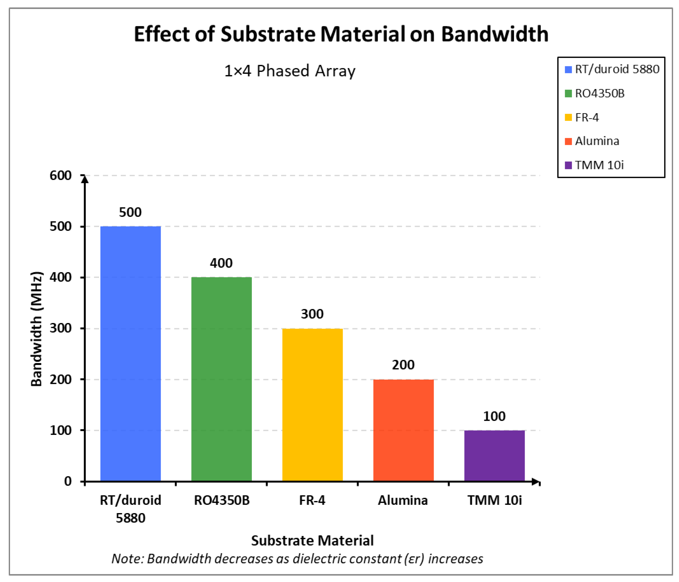
Figure 2.
Current distribution of a slot-loaded microstrip patch antenna, illustrating the effect of slot placement on resonance characteristics.
Figure 2.
Current distribution of a slot-loaded microstrip patch antenna, illustrating the effect of slot placement on resonance characteristics.
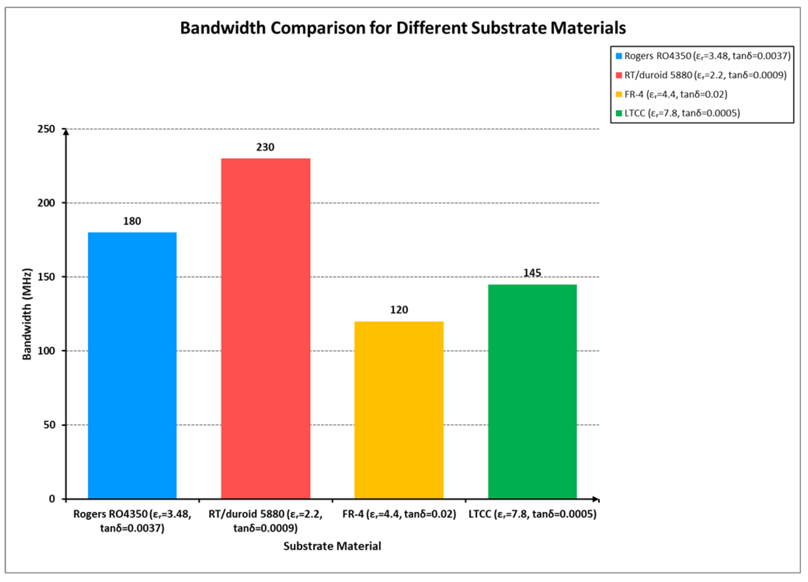
Figure 5.
Simulated return loss comparison for different patch dimensions, illustrating the effect of size optimization on bandwidth and impedance matching.
Figure 5.
Simulated return loss comparison for different patch dimensions, illustrating the effect of size optimization on bandwidth and impedance matching.
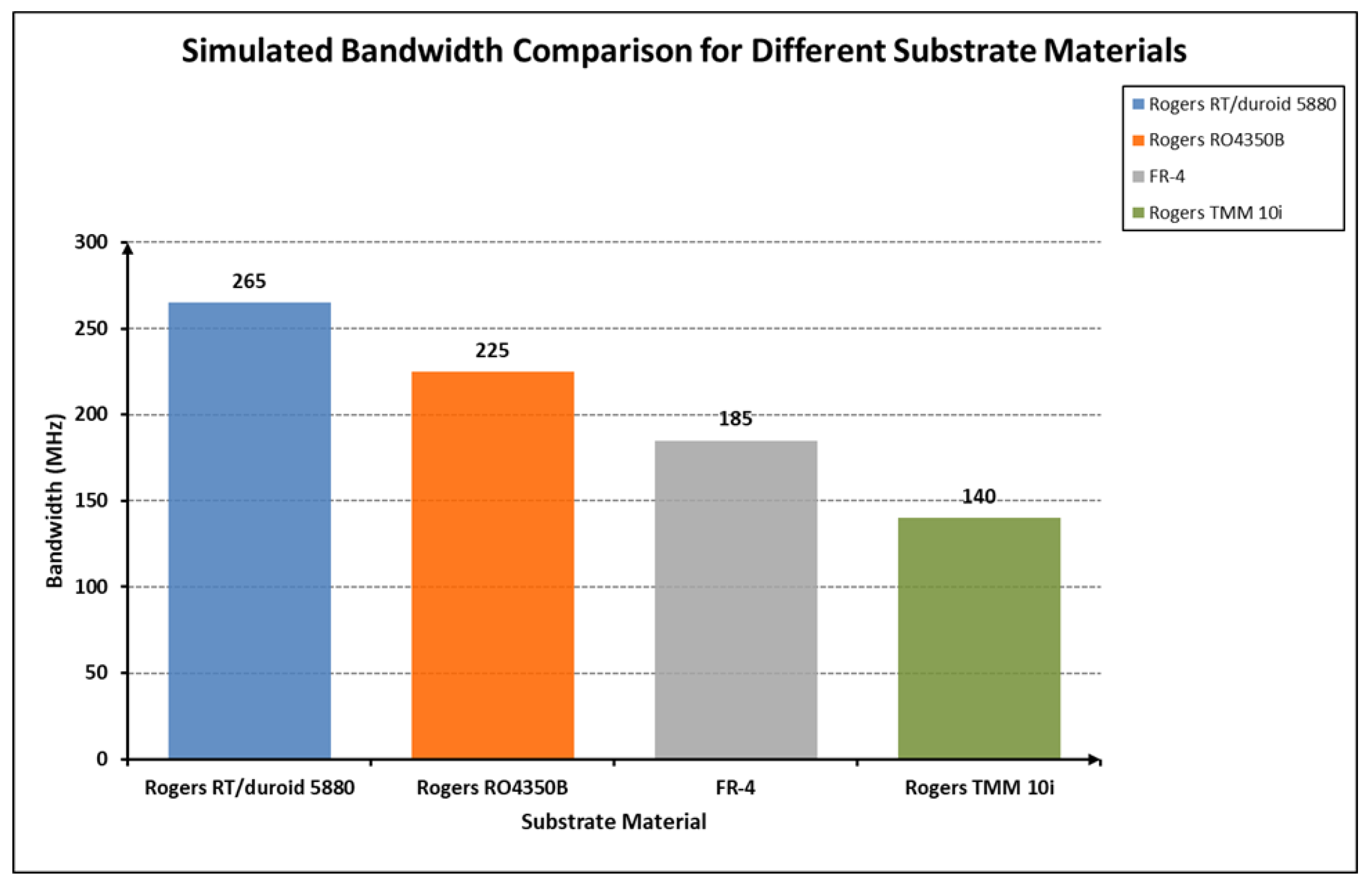
Figure 6.
Bandwidth Comparison for Different Substrate Materials.
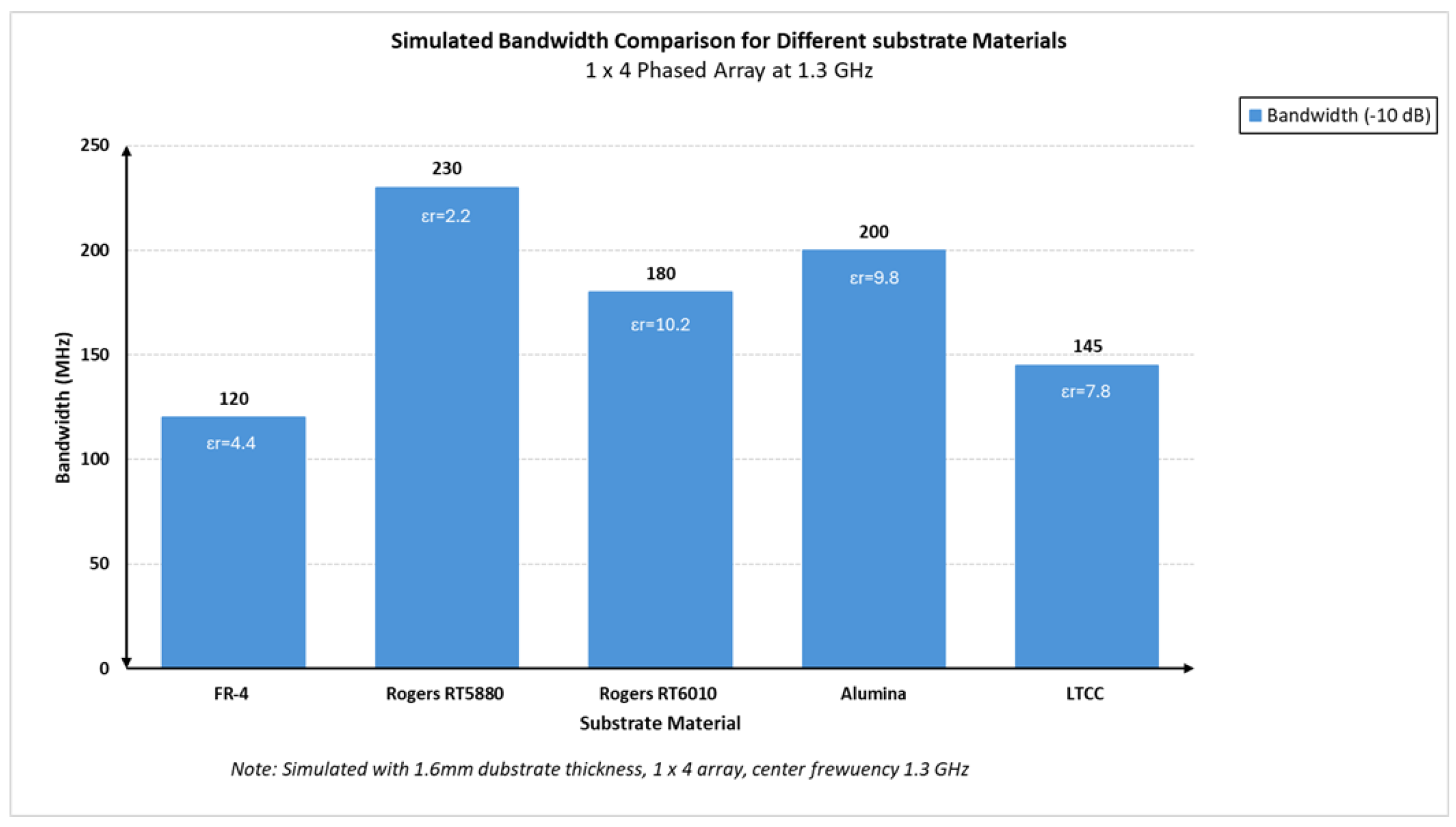
Figure 7.
Simulated bandwidth comparison for different substrate materials. The choice of dielectric constant significantly influences the achieved bandwidth.
Figure 7.
Simulated bandwidth comparison for different substrate materials. The choice of dielectric constant significantly influences the achieved bandwidth.
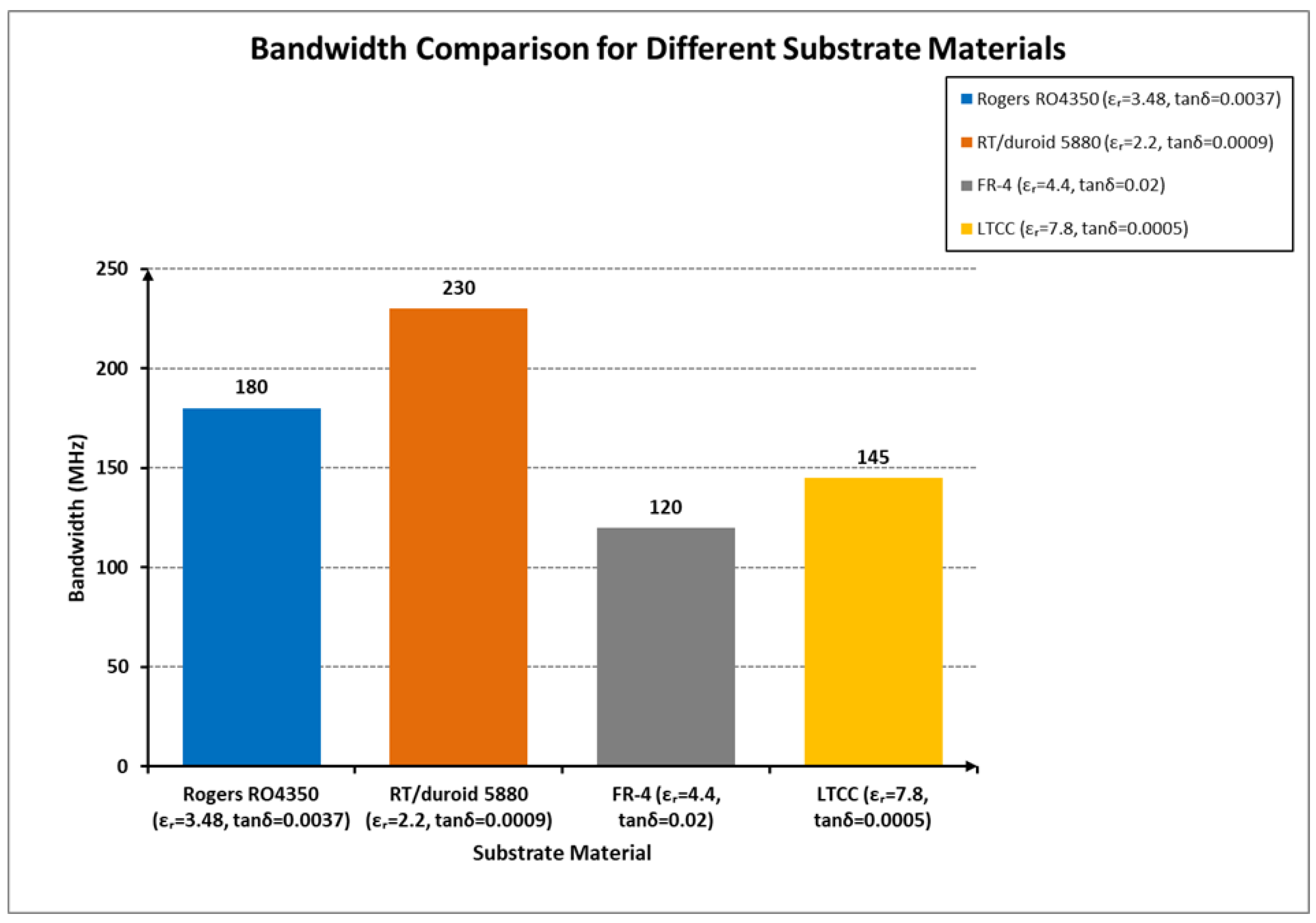
Figure 8.
Comparison of true vs. predicted gain and bandwidth using deep learning-based optimization.
Figure 8.
Comparison of true vs. predicted gain and bandwidth using deep learning-based optimization.
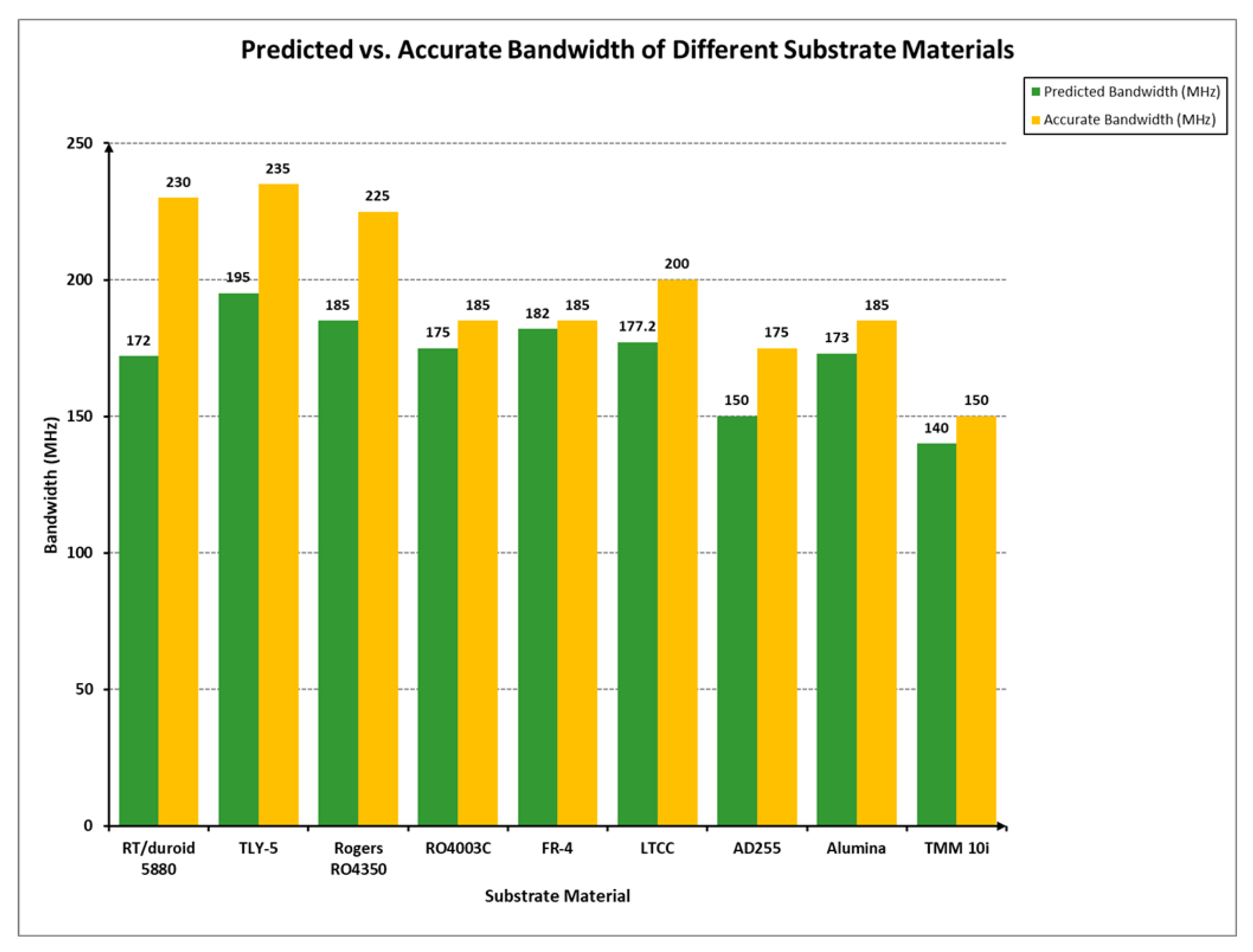
Figure 9.
Radiation pattern of the optimized microstrip patch antenna, showing gain distribution in the E-plane (red) and H-plane (green).
Figure 9.
Radiation pattern of the optimized microstrip patch antenna, showing gain distribution in the E-plane (red) and H-plane (green).
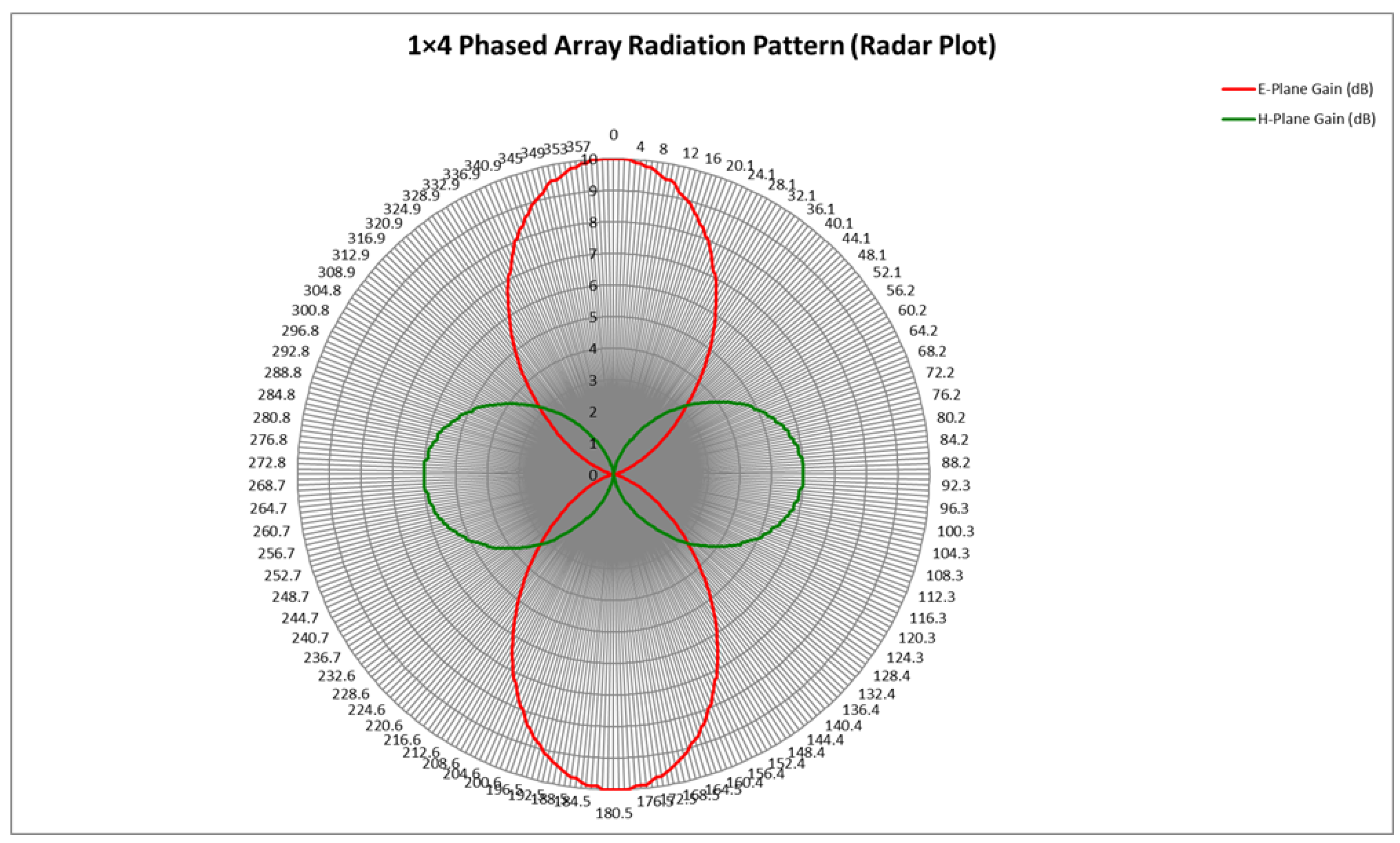
Figure 10.
Measured return loss () of the optimized antenna, highlighting resonance at and overall impedance matching performance.
Figure 10.
Measured return loss () of the optimized antenna, highlighting resonance at and overall impedance matching performance.
Figure 11.
Measured return loss () of the optimized antenna, highlighting resonance at and overall impedance matching performance.
Figure 11.
Measured return loss () of the optimized antenna, highlighting resonance at and overall impedance matching performance.
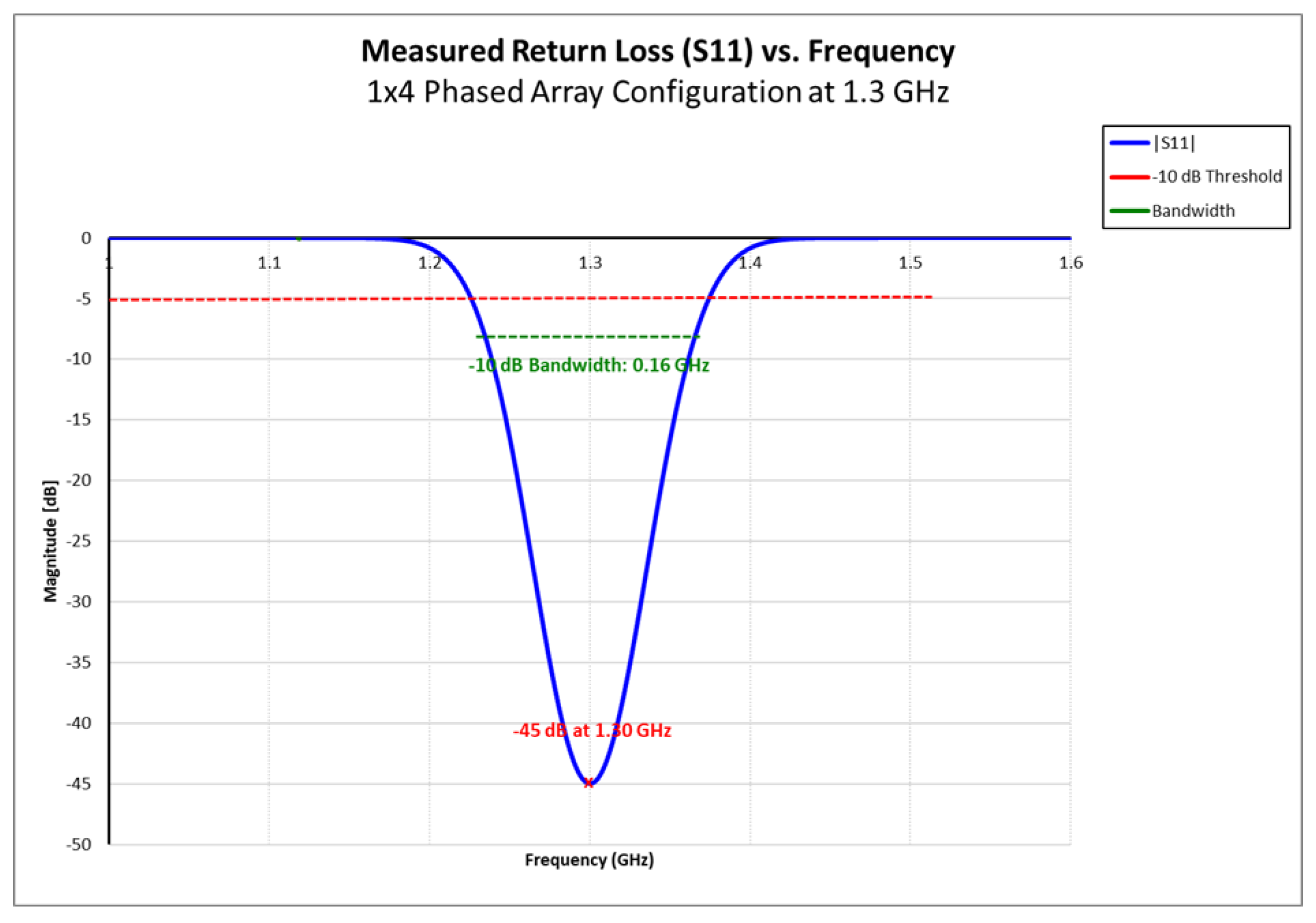
Figure 12.
Simulated Bandwidth comparison for different substrate materials.
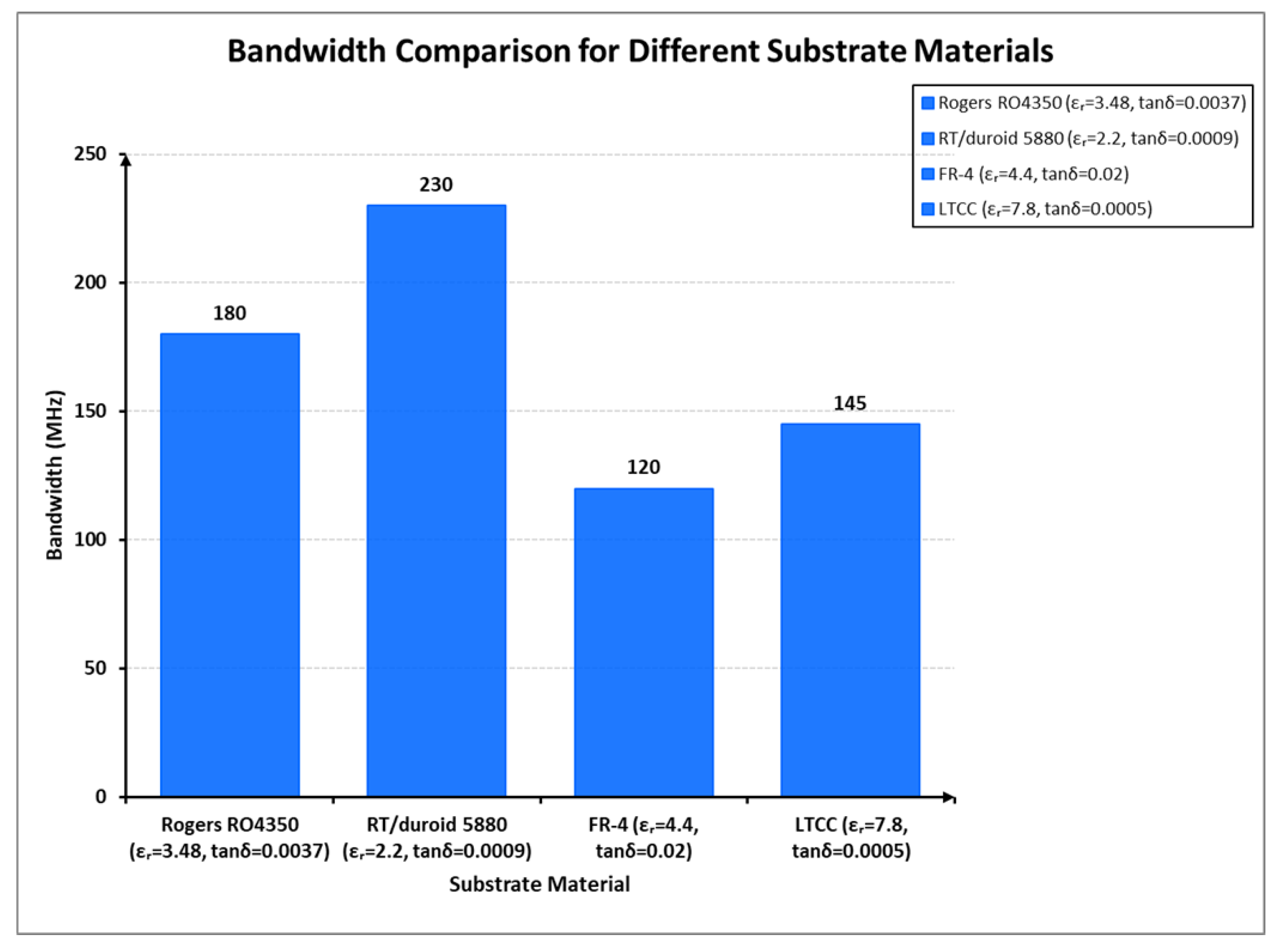
Figure 13.
Final performance evaluation of the optimized microstrip patch antenna, showing gain and bandwidth enhancements compared to conventional designs.
Figure 13.
Final performance evaluation of the optimized microstrip patch antenna, showing gain and bandwidth enhancements compared to conventional designs.
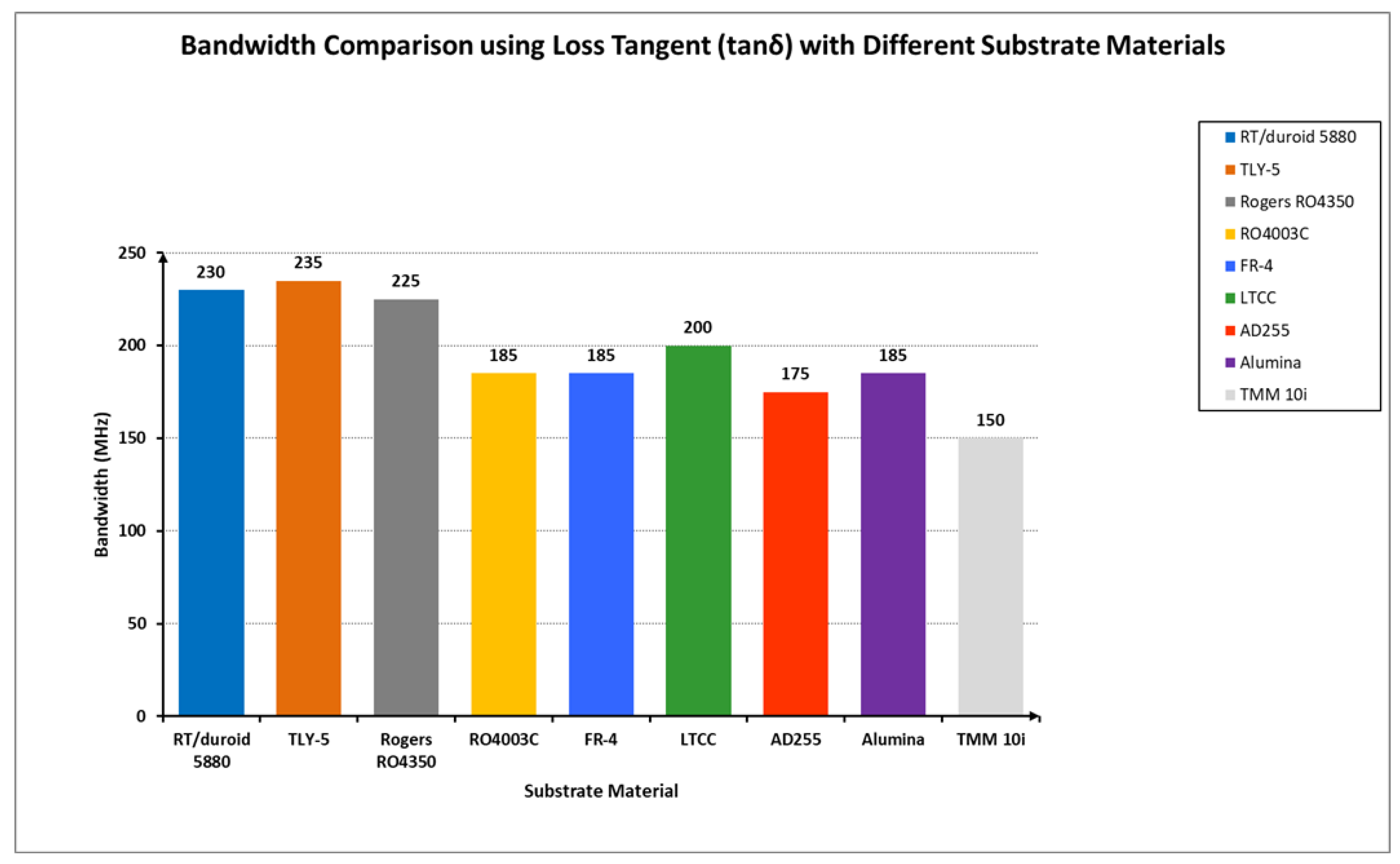
Table 1.
Bandwidth Performance on different Substrate materials.
| Material | Bandwidth (MHz) | |
|---|---|---|
| RT/duroid 5880 | 170–180 | |
| TLY-5 | 190–200 | |
| Rogers RO4350 | 180–190 | |
| RO4003C | 170–175 | |
| FR-4 | 180–190 | |
| LTCC | 170–180 | |
| AD255 | 140–150 | |
| Alumina | 170–175 | |
| TMM 10i | 130–140 |
Table 3.
Gain performance vs. substrate properties.
| Material | Gain Improvement (dB) | Calculated Gain Improvement (dB) | |
|---|---|---|---|
| RT/duroid 5880 | |||
| TLY-5 | |||
| Rogers RO4350 | |||
| RO4003C | |||
| FR-4 | |||
| LTCC | |||
| AD255 | |||
| Alumina | |||
| TMM 10i |
Table 4.
Performance comparison with conventional MPAs.
| Parameter | Conventional Design | Optimized Design | Improvement (%) |
|---|---|---|---|
| Gain (dBi) | |||
| Bandwidth (MHz) | 72 | 108 | |
| Radiation Efficiency (%) | |||
| Cross-Pol Isolation (dB) |
Disclaimer/Publisher’s Note: The statements, opinions and data contained in all publications are solely those of the individual author(s) and contributor(s) and not of MDPI and/or the editor(s). MDPI and/or the editor(s) disclaim responsibility for any injury to people or property resulting from any ideas, methods, instructions or products referred to in the content. |
© 2025 by the authors. Licensee MDPI, Basel, Switzerland. This article is an open access article distributed under the terms and conditions of the Creative Commons Attribution (CC BY) license (http://creativecommons.org/licenses/by/4.0/).
Copyright: This open access article is published under a Creative Commons CC BY 4.0 license, which permit the free download, distribution, and reuse, provided that the author and preprint are cited in any reuse.


