Preprint
Article

This version is not peer-reviewed.

Mixed Pt-Ni Halide Perovskites for Photovoltaic Application

A peer-reviewed article of this preprint also exists.

Submitted:

17 November 2024

Posted:

19 November 2024

You are already at the latest version

Abstract

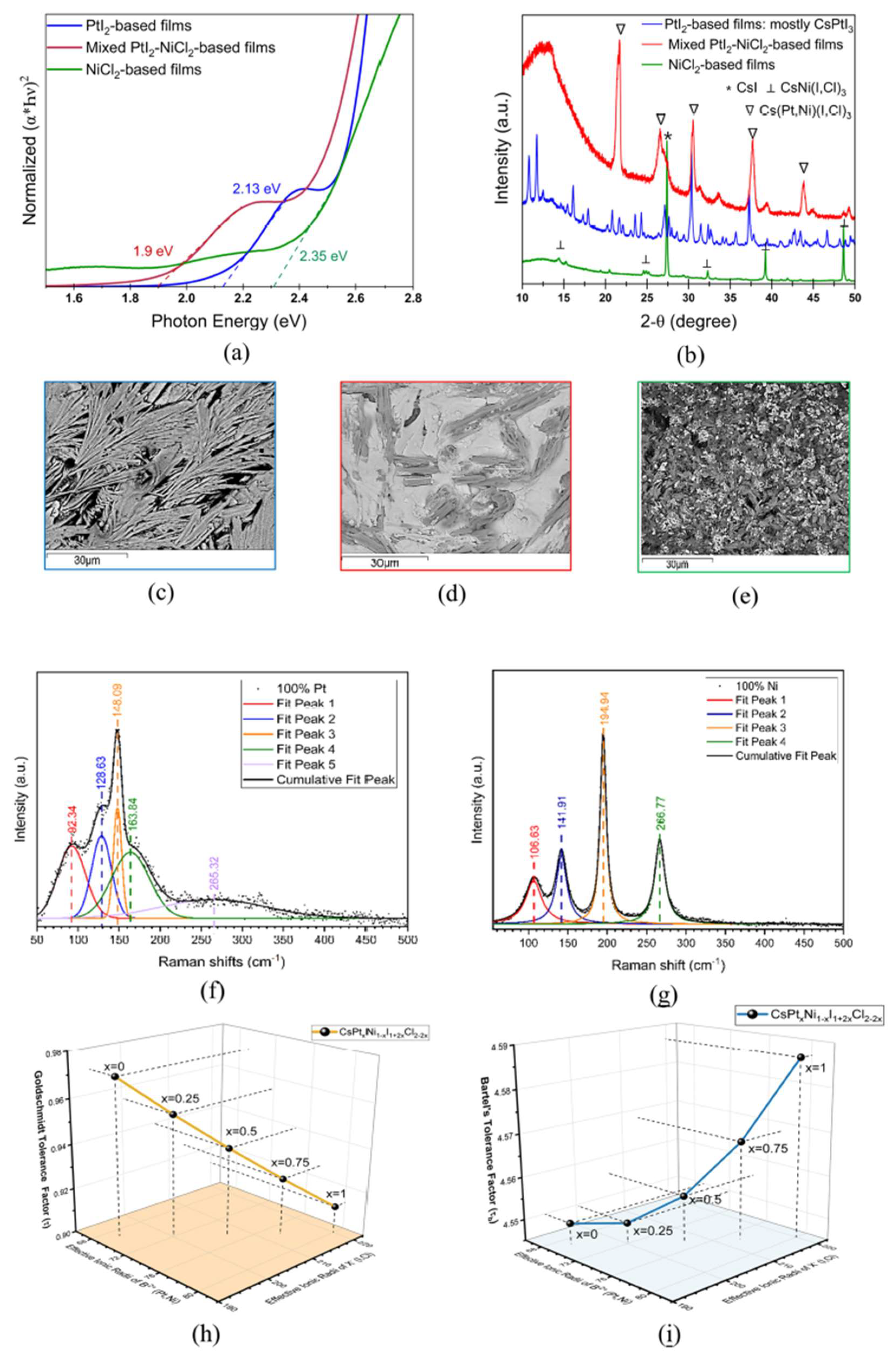
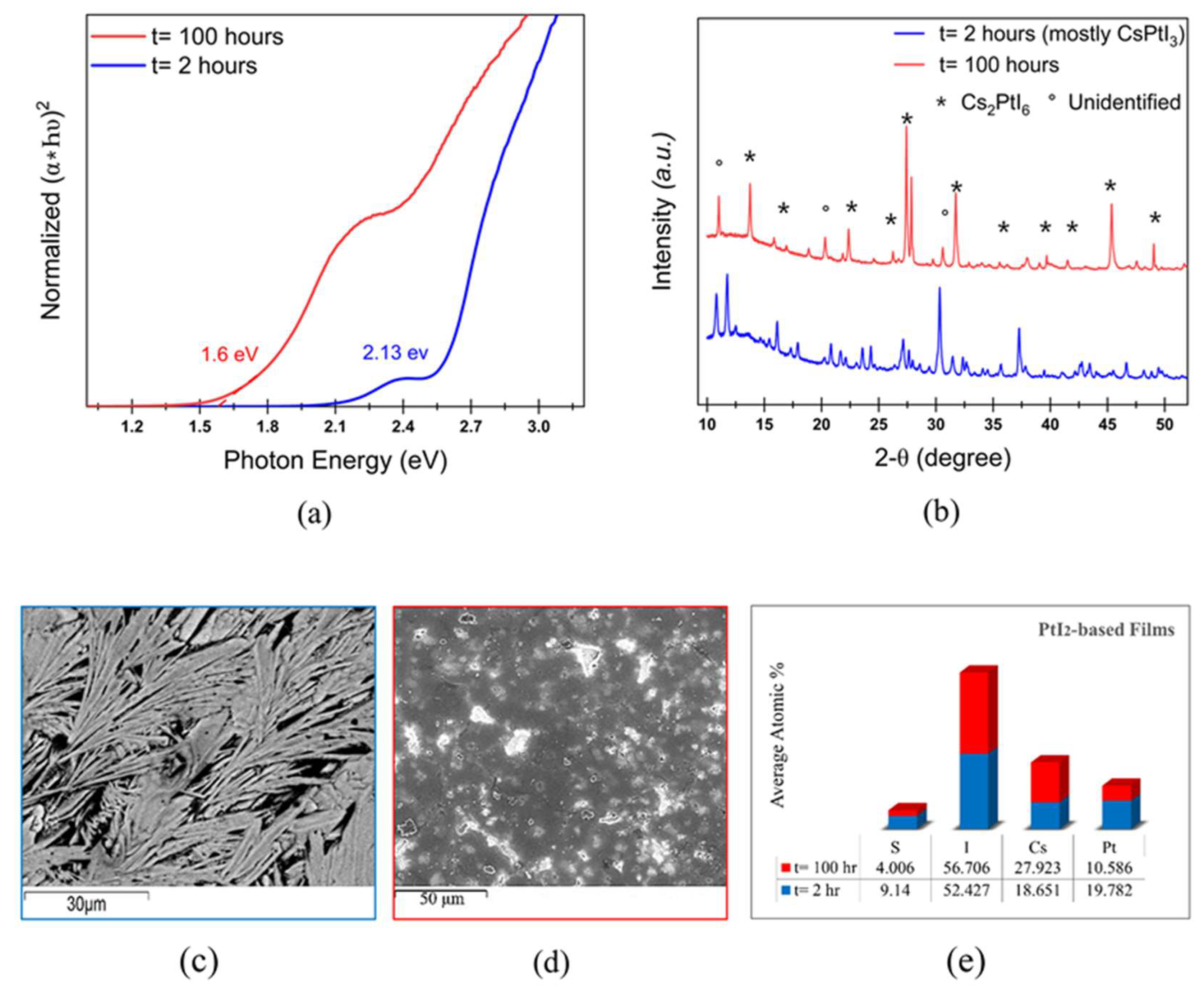
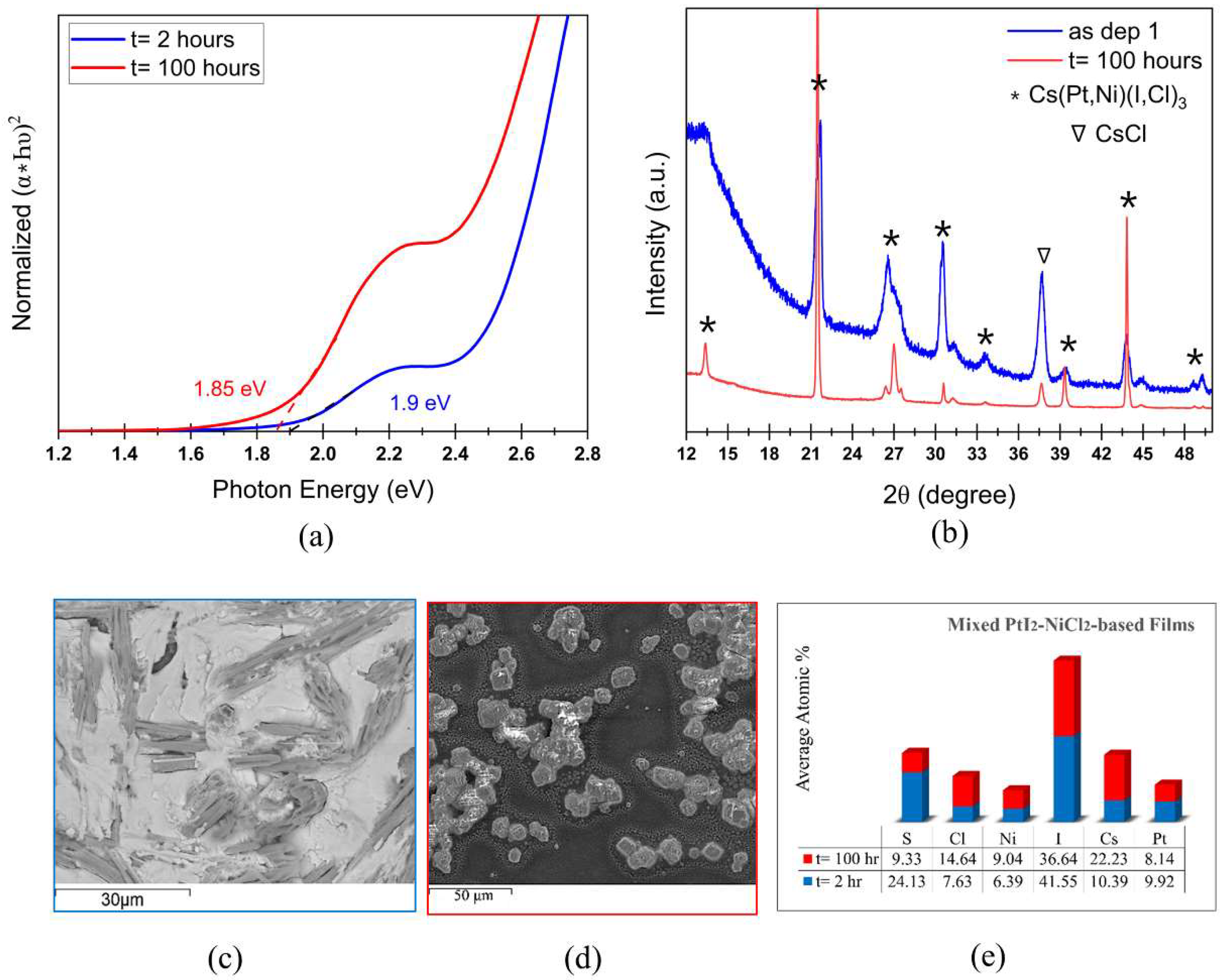
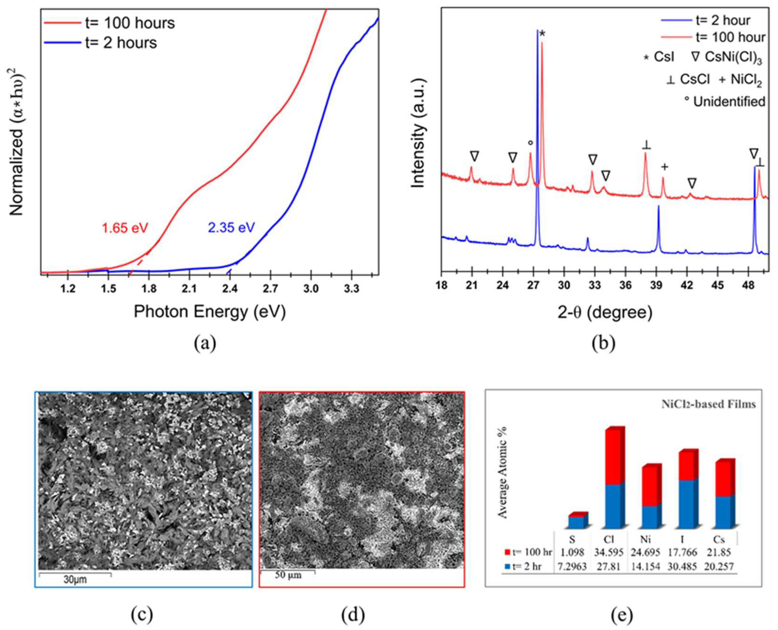
Cs2PtI6 is a promising photoabsorber with direct bandgap of 1.4 eV and high carrier lifetime, however, the cost of Pt inhibits its commercial viability. Here, we explore the effect of replacing Pt with earth-abundant Ni in solution-processed Cs(PtxNi1-x)(I,Cl)3 thin-films on the properties and stability of the perovskite material. Films fabricated with CsI and PtI2 precursors result in perovskite phase with bandgap of 2.13 eV which transitions into stable Cs2PtI6 with a bandgap of 1.6 eV upon annealing. Complete substitution of PtI2 in films with CsI + NiCl2 precursors results in a wider bandgap of 2.35 eV and SEM shows 2 phases- a rod-like structure identified as CsNi(I,Cl)3 and residual white particles of CsI, also confirmed by XRD and Raman spectrum. Upon extended thermal annealing, the bandgap reduces to 1.65 eV and transforms to CsNiCl3 with a peak shift to higher 2-theta. Partial substitution of PtI2 with NiCl2 in mixed 50-50 Pt-Ni-based films produces a bandgap of 1.9 eV exhibiting a phase of Cs(Pt,Ni)(I,Cl)3 composition. A similar bandgap of 1.85 eV and the same diffraction pattern with improved crystallinity is observed after 100 hours of annealing, confirming the formation of a stable mixed Pt-Ni phase.

Keywords: 
;  ;  ;  ;  ;  

1. Introduction

In recent years, perovskite photovoltaic technology has offered enormous viability and dimensionality in solar cell research. Perovskite, as a light-harvesting active layer, generated remarkable development in device efficiency of 25.6% in the single-junction solar cell, and over 33% in perovskite/silicon tandem solar cell [1,2]. Also, all-perovskite tandem solar cell is showing great potential in device performance and so far achieved a power conversion efficiency (PCE) of 26.4% with a wide bandgap (WBG) FA0.8Cs0.2Pb(I0.62Br0.38)3 perovskite as the top subcell (1.8 eV) and thermally mixed Sn/Pb narrow bandgap (NBG) FA0.7MA0.3Pb0.5Sn0.5I3 perovskite as the bottom subcell (1.2 eV) [3]. Transitioning photovoltaic technology from the laboratory to commercial products, high power conversion efficiency, low cost, long lifetime, and low toxicity are some of the critical factors to consider during material selection [4]. Pb-halide perovskites have been the most studied compositions in next-generation photovoltaics due to their excellent optoelectronic properties, such as the highest-power conversion efficiency (PCE) and ideal bandgap [5,6,7]. However, the practical relevance of these materials is hindered as they offer multifarious disadvantages, including toxicity, high water solubility and bioavailability, and thermodynamic instability of CH3NH3PbI3 in air [4,6,8,9]. To address the toxicity issue, Pb-free perovskite compounds have been the mainstay of the perovskite research study. Among the several alternative cations to Pb from group-14 elements, the Sn-based perovskite absorbers are the widely studied alternative which work superior in achieving high efficiency due to its isoelectronic configuration of s2p2 similar to Pb and smaller radius (1.35 Å and 1.49 Å in Sn2+ and Pb2+ respectively) [10,11]. Due to its smaller size than Pb, incorporating Sn in ASnPbX3 system increases the tolerance factor and decreases the bandgap [12]. However, the high oxidation tendency from Sn2+ to Sn4+ upon exposure to air and the energy band levels mismatch between the perovskite and charge transport layers generate large recombination at the grain boundaries in Sn-based perovskites and hence lower PCE than that of Pb-based perovskites [10,13]. Recently, transition metal-based double perovskite, Cs2PtI6, has emerged as another potential alternative to Pb-free perovskite owing to their experimentally produced direct narrow bandgap of 1.37 eV [14] and 1.4 eV [15]. Our previous work reported an atmospherically processable Cs2PtI6 perovskite device with an excellent absorption coefficient of 4 × 10⁻⁵ cm−1 and the highest efficiency of 13.88% [15]. A high Voc comparable to Pb-based perovskite device and a high minority carrier lifetime of over 2.8 μs with ethylene diamine (EDA) achieved in our study revealing Cs2PtI6 as a competitive Pb-alternative for high-performance halide perovskite solar cells (HPSCs). Our theoretical investigation revealed key strategies, such as eliminating parasitic losses and optimizing band offset, to achieve a Cs2PtI6 photoabsorber with a PCE over 26% [16]. However, due to the high cost of Pt, the Cs2PtI6 perovskite is viable mostly as a model system [15]. Several other transition metals, such as copper (Cu), silver (Ag), nickel (Ni), palladium (Pd), etc., have been reported in a few studies. Nag et al. studied inorganic double perovskite with monovalent Ag and trivalent Bi (i.e., Cs2AgBiX6), showing analogous optoelectronic properties similar to CsPbX3 with eco-friendly nature and long carrier lifetime [17]. However, it exhibits indirect bandgap with low optical properties leading to a low power conversion efficiency [18,19]. Soni et al. [20] numerically studied several transition metal-based halide double Cs2ZSbX6 perovskites for photovoltaic applications, with Z= Ag and Cu. The bandgap reduction by replacing Ag (2.542 eV) with Cu (1.299 eV) in the B-site and X= Cl was attributed to the high absorption of incident photons in the broad optical spectrum within the framework of their DFT analysis [20]. Having high dielectric constants of about 5.33 and 6.30 for Cs2AgSbI6 and Cs2CuSbI6 respectively and being optically active in the visible and ultraviolet regions, these materials can be productively utilized for optoelectronic devices [20]. CsNiCl3 and CsNiBr3 perovskites exhibiting low electronic bandgap and dispersive band edges are expected to offer attractive photovoltaic characteristics [21]. The use of precious metals impedes the commercialization progress of perovskite solar cells. Non-precious transition metals are promising candidates for the counter electrode of perovskite solar cells owing to their cost-performance ratio. Low-cost non-precious transition metals are investigated in several studies to replace expensive metals, such as gold (Au) or silver (Ag), as counter electrode materials in perovskite solar cells. Wang et al. [22] prepared perovskite solar cells with transition metals, such as Cu and Ni, and presented satisfactory performance with the power conversion efficiency of 13.04 and 12.18%, respectively, compared to that of 15.97% of the perovskite solar cell with Ag counter electrode. Ni, having a very close work function (∼5.04 eV) to that of Au (∼5.1 eV), showed a power conversion efficiency (PCE) of 10.4%, very comparable to devices with Au electrodes (11.6%) [23]. Cu-based perovskites are particularly advantageous because of their lower toxicity, magnetic properties [24], enhanced structural flexibility, and greater stability against light and humidity compared to Sn-based perovskites [25,26]. Several research groups have explored the use of Cu-based layered perovskites in the application of superconductors [25,27,28]. Cu, having a higher work function (~4.63 eV) than Ag (~4.23 eV), offers higher voltage output [22]. Perovskite materials also show promise in gas sensor applications due to their unique electrical and catalytic properties [29,30]. Among various target gases, the detection of hydrocarbons is significantly important in various applications. For example, monitoring dissolved gases (CH4, C2H4, C2H2, CO, CO2, and H2) by gas-in-oil analysis in transformer provides important information about transformer status [31,32]. Moreover, the detection and control of ethylene gas in agriculture are extremely important as emissions of this gas indicate the maturity state of fruits [33]. Ni-based perovskites are potential candidates for gas sensing applications, as NiI2 exhibits large impedance change in the ultra-low humidity environment [34]. Several research groups have developed lanthanum-transition metal perovskites, such as La-Co-based perovskite systems in the application of catalytic oxidation and combustion [35,36,37]. However, not enough information is available in the literature on Ni-based perovskites for photovoltaic applications. For the A-site cations, formamidinium (FA), methyl ammonium (MA), and cesium (Cs) are considered the most preferable elements to form perovskite structures due to the preferred tolerance factor in the range of 0.8 to 1. [FAPbI3 (t ~ 0.99), CsPbI3 (t ~ 0.8) MAPbI3 (t ~ 0.9)] [38,39]. CH3NH3I has a high decomposition rate into CH3I and NH3 at low temperatures [40], and the unstable photoactive black cubic phase of FA-based perovskites transitions into the photoinactive yellow phase at room temperature [41]. Cation-enabled perovskite black phase stabilization by partially incorporating inorganic Cs+ cation has been proven effective to enhance the photo and moisture stability of perovskite [42]. The purpose of this study is to assess how partially replacing Pt in cesium platinum triiodide (CsPtI3) perovskite with different concentrations of earth-abundant and low-cost nickel (Ni) influences its crystallographic and optoelectronic properties. Considering a partial replacement of Pt2+ sites by Ni2+ should not emerge severe lattice distortion due to a similar ionic radius of Ni2+ in comparison to the Pt2+ (Ni2+ vs Pt2+: 72 pm vs 80 pm) and we assume Ni2+ could likely incorporate within the perovskite crystal lattice, given high solid solubility of Pt and Ni. Cai et al. [43] performed first-principles calculations of halide perovskite-derived A2BX6 inorganic compounds to investigate the trends in bandgaps and energetic stability with chemical compositions providing guidelines for the design of halide A2BX6 compounds for potential photovoltaic applications. According to it, perovskite compounds with X=I and B=Ni exhibit large energy above hull (Ehull) (29 meV) and were not experimentally observed. All experimentally reported compounds have zero or small values of Ehull, such as Cs2NiCl6 and Cs2PtI6 have zero Ehull. Adjusting the molar ratio of PtI2: NiCl2 in the mixed-metal perovskite may afford new pathways to tailor a cost-effective system. To our best knowledge, this is the first study on the partial substitution of Pt by Ni performed experimentally for photovoltaic application.

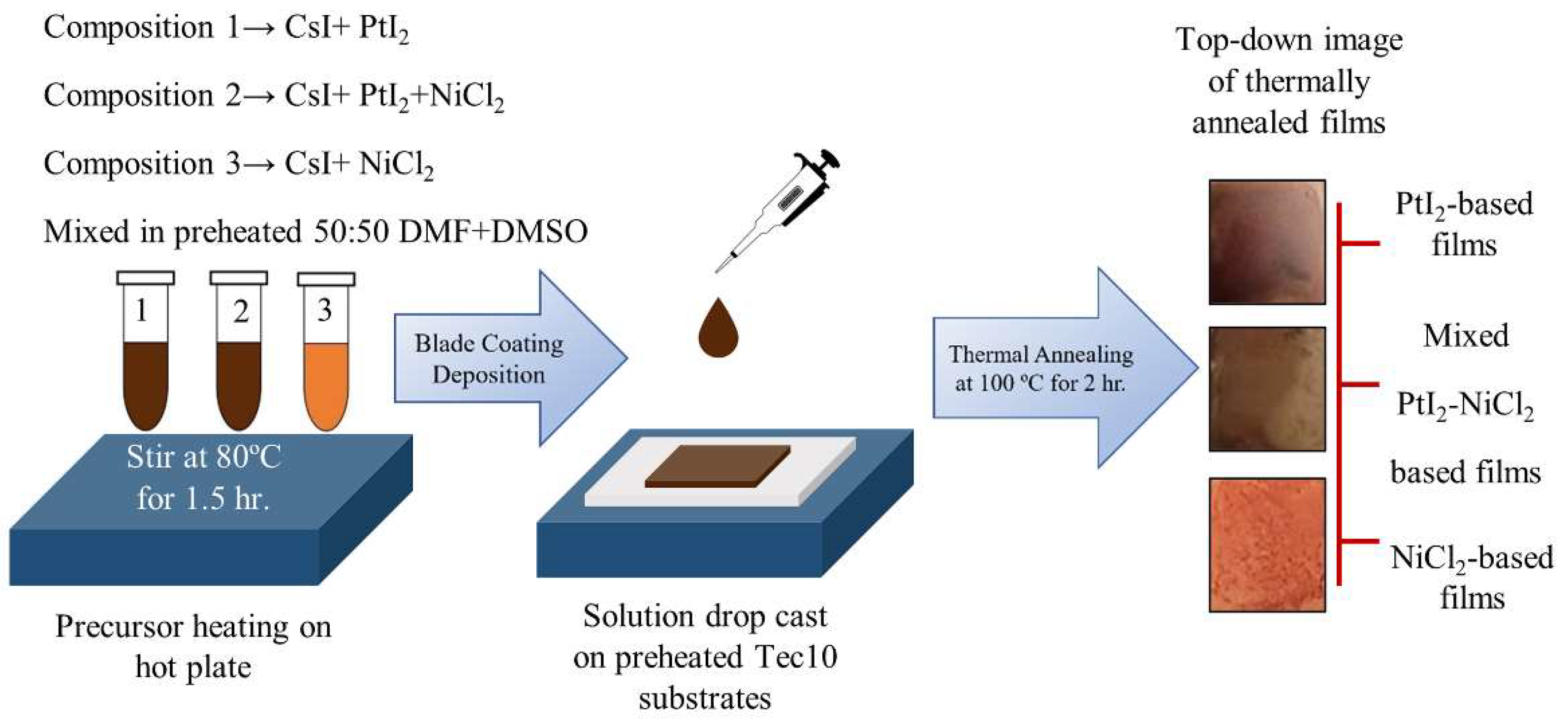
2. Materials and Methods

In this study, we have chemically synthesized three different perovskite compositions referred to as PtI2-based films, mixed PtI2-NiCl2-based films, and NiCl2-based films. All the films were fabricated via precursor-based solution processing under atmospheric conditions. The synthesis process of the 3 types of films is expected to be led by the following solid-state reactions, respectively:
CsI+ PtI2= CsPtI3,
CsI + xPtI2 + yNiCl2 = Cs(Ptx, Niy)(I, Cl)3,
CsI+ NiCl2= CsNi(I1Cl2),
where the x-to-y ratio of 50:50 has been used. The procedure and instruments for film fabrication and testing follow our previous works [15,44]. The precursor for the mixed PtI2-NiCl2-based films was prepared in a 0.25 M solution by the mixture of Cesium Iodide (0.06495 g), Platinum (II) Iodide (0.05611 g) and Nickel (II) Chloride (0.0162 g) with a molar ratio of 50:50 in 1 mL of pre-heated 50-50 Dimethylformamide (DMF)- Dimethyl sulfoxide (DMSO) solvent. The precursor mixture was heated at 75 °C for 1.5 h, followed by drop-casting on preheated Tec10 substrate. Doctor blade coating technique was used to spread the solution over the preheated substrates. Films were then annealed in a vacuum oven at -15 in Hg and 100 °C for 2 h. The same procedure has been followed to fabricate the PtI2-based and NiCl2-based films. The thermally annealed PtI2-based films and mixed PtI2-NiCl2-based films turned out in dark reddish-black color, and NiCl2-based films turned out orange color. For the stability testing, films were exposed to a dark thermal anneal test at 100 °C for 100 hours. All the solutes were purchased from Alfa-Aesar, Haverhill, MA, USA (Cesium Iodide, Alfa Aesar CAS: 7789-17-5; Platinum (II) Iodide, Alfa Aesar CAS: 7790-39-8; Nickel (II) Chloride, Alfa Aesar CAS: 7718-54-9; and solvents from Sigma-Aldrich, St. Louis, MO, USA (DMF, Sigma-Aldrich CAS: 68-12-2; DMSO, Sigma-Aldrich CAS: 67-68-5). The films were stored in a nitrogen-filled glove box before testing. X-ray diffraction spectroscopy (XRD) measurements were conducted on a Bruker diffractometer from Bruker Corporation Billerica, MA, USA under ambient conditions using Cu K radiation. EVA toolbox and Topas were used for XRD data analysis and phase identification. Shimadzu UV-2600 spectrometer was used to perform optical transmittance and reflectance measurements. The optical bandgap of the samples was determined by Tauc analysis. JEOL JSM-5610 was used to perform Scanning Electron Microscopy (SEM) and Energy Dispersive X-ray Spectroscopy (EDS) analysis. Raman spectra were measured at room temperature using the customized Scope Foundry-based Raman spectrometer at Molecular Foundry, Berkeley National Laboratory. The microscope was in confocal geometry with 1800g/mm grating and equipped with a silicon CCD. A continuous wave 532nm laser was used for excitation with 100uW (0.366mW/um2) and the 532nm long wave pass filter was set in the output path.
Figure 1. Atmospheric synthesis of PtI2, mixed PtI2-NiCl2, and NiCl2-based films in 50:50 DMF: DMSO via solution processing.
Preprints 139913 g001

3. Results and Discussion

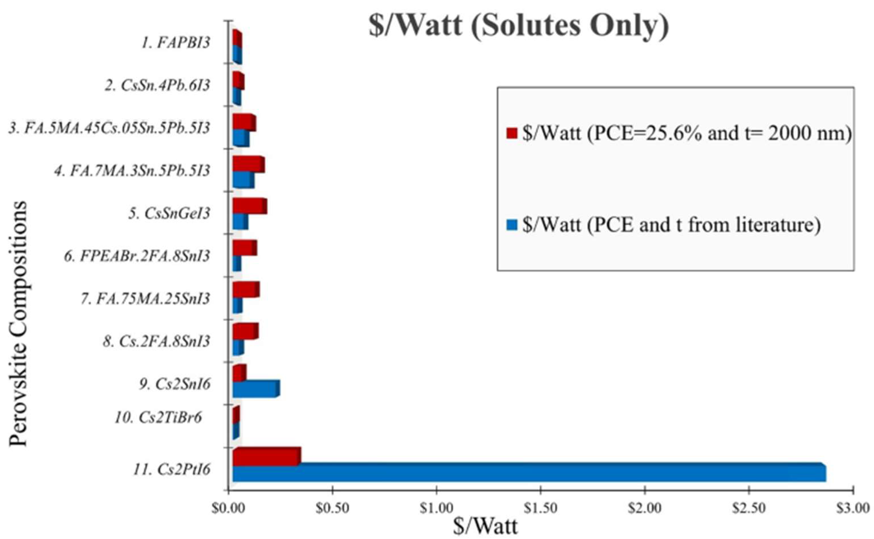
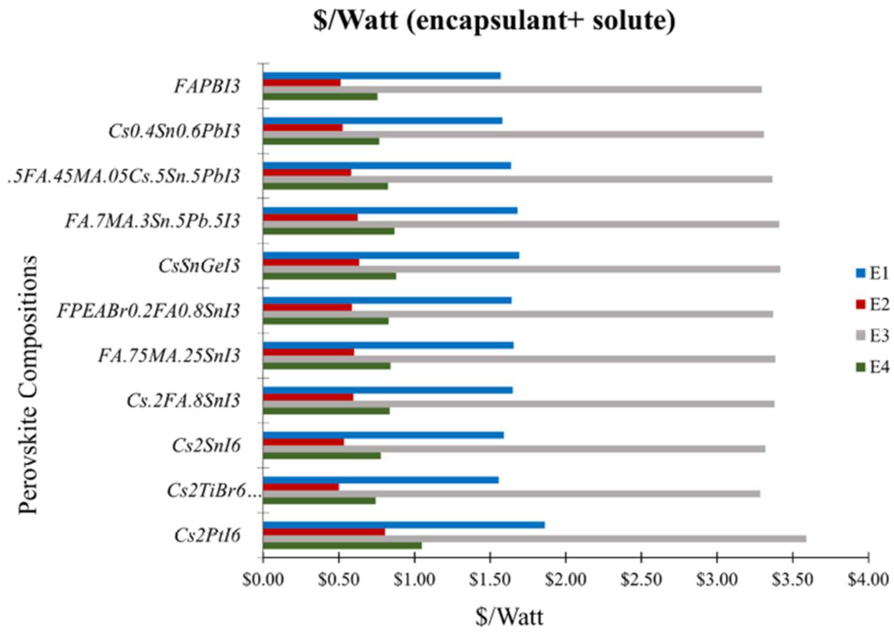
3.1. Cost Analysis of Solutes for Perovskite Precursor and Encapsulation for HPSCs

This cost model determines the $/watt of several perovskite material compositions, considering the molarity (M), absorber layer thickness (t), active cell area, and power conversion efficiencies (PCEs) from the respective literature. In this cost analysis, we compared the $/watt value associated with the precursor solutes required to prepare these compositions and the additional cost of four different encapsulants. Cost per gm of solutes and properties of perovskite compositions are summarized in Table S1 and S2, respectively. The molarity used in the literature for respective material compositions remains constant throughout this analysis. We also evaluated the $/watt with the value of PCE (25.6 %) and t (~ 2 µm) optimized to the value of the state-of-art FAPbI3 HPSCs [2]. The cost per unit volume is determined by the perovskite (product) volume, the proportional amount of reactants needed to achieve the product volume, and the cost of solutes per gram. The amount of perovskite, by moles, is determined using the known molecular mass (g/mol) and density (g/cm3) of the product seen in Equation (4).
M o l e s   o f   P e r o v s k i t e c m 3 m o l   / c m 3 = D e n s i t y     g / c m M o l a r   m a s s   g / m o l
Figure 2 is the graphical representation of the comparison of the $/watt of the precursor solutes required to prepare several perovskite compositions considering two cost frameworks. The 1st cost framework (blue) represents the $/watt when both the PCE and absorber layer thickness (t) were derived from the corresponding literature respective to each perovskite composition. The 2nd cost framework (red) represents the $/watt considering each perovskite composition matches both the PCE of 25.6% and t of 2000 nm as reported for the state-of-art FAPbI3 perovskite.
It is important to note that the overall cost associated with perovskite products depends on many other several things, such as the precursor synthesis methods, processing conditions, film stability, use of additives and encapsulations, etc. Our current analysis of $/watt only associates the cost of solutes used for the corresponding precursor. According to Figure 2 (blue), the $/watt of Cs2PtI6 is estimated to be ~144x more expensive than that of FaPbI3 perovskite. The synergistic effect of a thicker absorber layer of 10,000 nm and the high cost of PtI4 chemical compound (PtI4= $226.55/gm, PbI2= $1.176/gm) are responsible for the high $/watt of its precursor. The distinct impact of the PCE and t on the cost modeling is presented in Figure S1. According to it, if the t of the Pt-based composition remains constant at 10,000 nm and the PCE increases to 25.6%, the $/watt reduces by almost half times the initial $/watt value. Alternatively, if the PCE remains constant at 13.88% and t reduces to 2000 nm, the $/watt of Cs2PtI6 reduces by almost five times the initial $/watt value with the reported PCE and t. A thicker absorber layer requires more product and hence the t and cost of the solutes play a vital role in regulating the perovskite precursor cost. Our previous study numerically optimizes the thickness of several perovskite absorbers needed to reach the state-of-the-art PCE [16]. If both the parameters are optimized (PCE to 25.6% and t to 2000 nm), the $/watt of Cs2PtI6 is estimated to be only ~15x more expensive than the FaPbI3 perovskite, as indicated in Figure 2 (red) and reduces by almost nine times the initial $/watt value with the reported PCE and t.
In the most efficient HPSCs with the best PV performance, PbI2 is the main Pb-containing decomposition product, and thus is likely the main product to leak from broken solar modules due to its easy water solubility. the U.S. Environmental Protection Agency (EPA) has identified lead as one of 15 pollutants often found in publicly owned treatment works (POTW) and sewage that it considers a potential pollutant of concern [45]. The PbI2 solubility in water is 0.76 g L–1 at 20 °C [46], while the maximum accepted levels of Pb in drinking water are set as 5 orders of magnitude lower, at 0.000015 g L–1 (15 ppb) by EPA [45]. These numbers manifest the importance to limit the possible leaching of dissolved Pb-containing products from HPSCs into the environment. A strategy to mitigate Pb leaching from HPSCs into the environment is through the use of encapsulants. Also, encapsulation for solar panels is a critical issue for the long-term operational stability of HPSCs. In the second phase of this cost analysis, we evaluated perovskite cost with four different cost-effective and commercially available polymer-based encapsulants viable for academic research, such as ethylene–vinyl acetate (EVA), Polyolefin (TPO), Polytetrafluoroethylene (PTFE) known by its trade name Teflon®, and Polyethylene terephthalate (PET).
Currently the most common polymeric encapsulant material used in commercial silicon solar modules is EVA, due to its low-cost and easy processability [47,48]. It offers low water vapor transmission rate (WVTR) compared to some other encapsulants reported in the literature but high water diffusion rate causing a possible decline in module lifetime [49]. Also, its sensitivity to discoloration under UV radiation results in decreased light-transmittance, and therefore reduced solar cell power output [48]. Polyolefin is a commonly used encapsulant in academic research and has several advantages like good adhesion energy, creep failure resistance, low WVTR, low discoloration rate and better light transmittance compared to EVA [50,51,52].
Studies report the unique use of hydrophobic fluoropolymer, PTFE, for improving the perovskite crystallinity and passivating defects when used an optimum amount of it as an additive in the perovskite organic precursor [53]. Studies also reports that hydrophobic passivation of PTFE precursor solution prevents PbI2 decomposition and improved moisture stability [54]. However, it is sensitive to electrophilic attack upon reaction with alkali metals when exposed to long hours of heat [55]. Several studies have used PET in a hybrid encapsulation framework in a combination with transparent metal oxide films (e.g., Al2O3) or inorganic/organic multilayers and reported its compatibility to be used on flexible substrates [56,57,58], however it comes comparatively costlier than the previously mentioned encapsulants. The $/m2 of these encapsulants is summarized in Table S3. Recent improvements in perovskite stability through these encapsulants is summarized in Table S4. There are many other effective encapsulants being studied for stability improvement in perovskite. A comprehensive cost analysis with additional highly efficient encapsulants will be discussed in a future review paper.
Figure 3 is the graphical representation of the $ per watt of solutes with added encapsulant cost of several perovskite compositions considering each perovskite composition with optimized PCE of 25.6% and t of 2000 nm as reported for the state-of-art FAPbI3 perovskite. If both the parameters are optimized, the $/watt of (solute+ encapsulant) Cs2PtI6 is estimated to be only ~1 %-1.4 % more expensive than the FaPbI3 perovskite for four different encapsulants. Among them, The most expensive PET renders a cost of ~$3.6/watt for Cs2PtI6 ($3.3/watt for FAPbI3) and the least expensive Teflon renders a cost of ~$0.81/watt for Cs2PtI6 ($0.516/watt for FAPbI3), which are ~2.5x and ~4.7x cheaper than the $/watt value of solutes+ encapsulants with its reported PCE of 13.88% and t of 10,000 nm as outlined in Figure S2. The calculated precursor cost of FAPbI3 with expensive encapsulants like PET ($3.29/watt) exceeds that of the unencapsulated Cs2PtI6 ($2.89/watt). Figures S3 and S4 represent the $/watt value (solute+ encapsulant) with the discrete effect of the optimized PCE and optimized absorber layer thickness reported for the Pb-based FAPbI3 perovskite, respectively.
The long-term operational stability investigated using maximum power point (MPP) tracking under a simulated 1-sun illumination for the unencapsulated FAPbI3-based PSC reports a loss of 15% of its initial efficiency, under continuous light soaking using a LED lamp for 450 hours at around 35 °C [2]. The unencapsulated Cs2PtI6-based Devices tested under AM1.5G at 65 °C for 500 h shows a loss of 23% of its initial efficiency. The shunts causing a decrease in Voc and FF after light soaking are expected to develop due to pinholes in the Cs2PtI6 films and can be improved with film quality [15]. Considering the high water solubility of the Pb-based compound, a strong and effective encapsulant system is needed which can potentially increase the overall cost. With comparable efficiency and t, Cs2PtI6 can be considered a suitable alternative to Pb-based perovskites despite the high cost associated with Pt-based solutes. However, considering the high cost associated with its current PCE and t, Cs2PtI6 is not viable for commercialization, and exploration for alternative compounds to replace Pt has immense research significance. In this paper, we have summarized the primary results corresponding to the partial replacement of Pt with Ni in the B-site.

3.2. Pt-Ni Mixing in Halide Perovskite

The bandgap analysis of our PtI2-based films, mixed PtI2-NiCl2-based films, and NiCl2-based films outlined in Figure 4a show a bandgap of 2.13 eV for PtI2-based films. The bandgap increases to 2.35 eV when NiCl2 entirely replaced PtI2. Alteration of the halide anion changes the bond distance and/or angle of X–B–X, and incorporation of smaller X-anion, such as Cl replacing I, increases the bandgap [59]. Our bandgap analysis of NiCl2-based films replacing PtI2 supports this theory. The partial substitution of NiCl2 with PtI2 in mixed PtI2-NiCl2-based films is supposed to exhibit a larger bandgap than that of the NiCl2-based films upon the incorporation of the larger Pt cation in the B-site. However, the reduced bandgap of 1.9 eV in mixed PtI2-NiCl2-based films is likely driven by the incorporation of the larger X-anion (I- in this case) rather than the larger B-cation. The XRD analysis of the 3 types of films is shown in Figure 4b. The XRD pattern shows mixed phases of many unidentified lower-intensity diffraction peaks with a partial match to Cs2PtI6 resulting in a higher relative noise level in the films prepared in CsI+PtI2 precursor and indicates poor crystallinity. A peak shift to higher angles in XRD can be attributed to the incorporation of B-site cations with larger ionic radii, leading to an expansion of the perovskite lattice [60,61,62]. Similar result is observed in our study with the incorporation of bigger Pt in the mixed PtI2-NiCl2-based films. The formation of Cs(Pt,Ni)(I,Cl)3 phase in the mixed PtI2-NiCl2-based films is confirmed by a peak shift of standard CsNiCl3 (a= 7.118 Å, b= 7.118 Å, c= 5.9085 Å ) to higher 2*theta. The diffraction peaks of this new phase are located in between CsNiCl3 and Cs2PtI6 phases, which implies the intercalation of Pt into perovskite lattice and formation of mixed Pt-Ni-based phase. (Table 1).
XRD spectra of a new phase of CsNi(I,Cl)3 forms with the complete substitution of Pt with Ni, suggested by a peak shift of standard CsNiCl3 to lower 2*theta. Peaks of CsNiCl3 located at 20.8°, 25° and 32.74° shifts to 20.51°, 24.59° and 32.3°, respectively, and forms this mixed anion phase in CsI+NiCl2 precursor. The peak located at 27.4° in the XRD pattern of the NiCl2-based films was identified as CsI (27.7°) with a peak shift to lower angle (27.39°). The wide bandgap in NiCl2-based films may also be ascribed to the presence of CsI. Cross-sectional SEM images of the 3 types of films are presented in Figure 4c–e. PtI2-based films have a long needle-like structure, which is completely different than our previous observation in films prepared in CsI+PtI4 precursor. This SEM morphology along with the XRD pattern and bandgap provides strong evidence that we are not making a pure phase of Cs2PtI6 with CsI+PtI2 precursor [15]. Raman spectroscopy measurements were also conducted on the NiCl2-based films and PtI2 based film, as shown in Figure 4f and g, respectively. The sharp Raman peaks detected on the NiCl2-based film around 107, 142, 195 and 267 cm-1 are in line with reported values from literatures [65,66,67]. The peak at 267 cm-1 matched well with the A1g modes of CsNiCl3; The peak near 195 cm-1 correlated to the E2g mode while the peak 142 cm-1 is attributed to the E1g modes of CsNiCl3 [65]. As the film system also contained I- (with the introduction of CsI), the unassigned peak at ~106.63 might come from Ni-I or CsNiI3 structure [68]. The Raman peaks on the PtI2-based film were also observed and fitted at 92, 129, 148, 164, and 265 cm-1, respectively. These peaks are also in line with reported values from literatures [69,70,71]. The peak at ~129 and ~148 cm-1 should be assigned to the symmetric Pt-I stretch in ν2 mode (Eg) and ν1 mode (A1g), respectively [69,71]. And the Raman shift peaks at ~93 and 160 cm-1 were also reported in Hexaiododiplatinate (II) salts A2Pt2I6 [69]. This structure consists of Pt2I6 units and the corresponding cation (Cs in our case), while the anions form edge-shared squares [72]. The peak at ~93 cm-1 might come from the asymmetric I-Pt-I bend in ν4 mode (T1u) [71]. In order to elucidate the phase formation in PtI2-based films, we performed EDS analysis showing the statistical distribution of calculated average at % of precursor elements in Figure S5. It indicates a phase with Cs:Pt:I in the intended precursor ratio of 1:1:3. However, no standard XRD pattern is available for CsPtI3 in the database, so our XRD analysis could not confirm the presence of this phase. Figure 4d shows two different microstructures, a dark rod-like structure, and a transparent plate-like structure, present in mixed PtI2-NiCl2-based films. Similarly, NiCl2-based films have dark rod-like microstructure with white particles on the film surface presented in Figure 4e. The EDS analysis performed in various spectrums of these films shown in Figures S6 and S7 indicates the bright white plate-like features (solid columns) have Cs-I-rich morphology, and the dark rod-like features (patterned columns) have Cl-Ni-rich morphology, which suggests that the insolubility of NiCl2 is responsible for the formation of the rod-like features. In our previous study on mixed Sn-Pb perovskite [44], a similar microstructure was observed as a result of the coagulation tendency of the Pb compound due to the insolubility of PbI2. The presence of excess Cs and I particles observed in EDS analysis further validates the presence of CsI as identified in the XRD spectra of the NiCl2-based films. The EDS analysis also suggests the presence of a higher at% of sulfur in the rod-like surfaces rather than in the white Cs-I-rich surfaces, both in the mixed PtI2-NiCl2-based and NiCl2-based films. Even NiCl2-based films have almost no sulfur present in their Cs-I-rich regions. However, the influence of sulfur in the formation of rod-like features is not clear yet. Moreover, we calculated the Goldshmidt and Bartel tolerance factor for the Cs(Ni,Pt)(I,Cl)3 films, as shown in Figure 4h and I, respectively. It should be noted that optimal stability range of the 3D perovskite structure is indicated in the window 0.8<t<0.9 for Goldshmidt factor [73], while Bartel’s tolerance factor <4.18 predicts stable perovskite phase [74]. The tolerance factors of the Cs(Ni,Pt)(I,Cl)3 films are outside the optical range, which might explain the phase separation we observed.
In order to demonstrate the effect of long thermal annealing, we performed a heat-stability test by annealing the films for 100 hours at 65°C and compared the optoelectronic features to that of the reference films that were annealed for 2 hours. Figure 5 indicates that the wide bandgap intermediate phase transforms to a stable Cs2PtI6 perovskite phase after the long hour of thermal annealing. Figure 5a exhibits a significantly reduced bandgap of 1.6 eV in the PtI2-based films exposed to long thermal annealing, which is in reasonable agreement with the bandgap of the Cs2PtI6 film (1.4 eV) reported in our previous work [15]. Figure S8 exhibits noticeably red-shifted absorption spectra, compared to the reference films, with an absorption edge at close to 900 nm confirming the suppressed bandgap achieved in thermally exposed films. It is known that crystallinity is critical for perovskite stability because the main defect-induced degradation starts near the grain boundaries [2]. The poor crystallinity in the reference PtI2-based films is consistent with poor optical measurements, which is improved with long hour thermal annealing. Upon thermal annealing, the PtI2-based films become more crystalline with a better match to the diffraction pattern of the Cs2PtI6 perovskite (11.361 Å) with some unreacted Cs residue (Figure 5b). The Cs2PtI6 phase was determined by the (111), (200), (220), (222), (400), (440), and (622) peaks. The amorphous morphology becomes compact including some Cs-rich white particles on top as confirmed by the SEM analysis in Figure 5c. The EDS analysis in Figure 5d further validates the formation of Cs2PtI6 in the thermally annealed films showing a phase of Cs:Pt:I at an atomic ratio of 2:1:6 with some excess Cs, which is well aligned with our XRD analysis.
The effect of thermal annealing on the optoelectronic properties of mixed PtI2-NiCl2-based films is demonstrated in Figure 6. Figure 6a shows red-shifted bandgap spectra rendering a bandgap of 1.85 eV, very close to the bandgap (1.9 eV) of the reference films annealed for 2 hours. Figure S9 shows thermally exposed films have a slightly red-shifted absorption opening with an absorption edge at close to 700 nm similar to reference films, possibly implying its stability against thermal annealing. The peak broadening of the XRD pattern is inversely correlated with crystallite size. Perovskite films with large crystallite sizes can have reduced grain boundaries and restrained carrier recombination, which increases carrier mobility [75]. Films exposed to extended thermal annealing have improved crystallinity, and narrow refined XRD spectra with a shift to higher angles as shown in Figure 6b, which can be correlated to reduced lattice parameters and is similar to our previous observation [44]. Similar to the reference films, thermally exposed films exhibit diffraction pattern in the same orientation of Cs(Pt,Ni)(I,Cl)3. The peak located at 37.56° in both of these films is attributed to the CsCl phase, which can be ascribed to the wider secondary bandgap. No significant change in the XRD pattern is observed, supporting our proposition of its thermal stability speculated through bandgap analysis. According to Figure 6c,d, the rod-like morphology transformed into a compact plate-like structure displaying white Cs-rich crystals on the surface. According to the EDS analysis in Figure 6e, a significant decline in the atomic distribution of sulfur content is observed after the thermal treatment. We attribute this to the evaporation of the DMSO solvent residue upon annealing which might be responsible for the refined and crystalline XRD spectra.
The effect of thermal annealing on the optoelectronic properties of NiCl2-based films is demonstrated in Figure 7. Figure 7a exhibits a significantly narrower bandgap of 1.68 eV in the films annealed for 100 hours, compared to the films annealed for 2 hours (2.35 eV). Figure S10 exhibits noticeably red-shifted absorption spectra with an absorption edge shifted from only 500 nm to 750 nm confirming the suppressed bandgap achieved in the thermally exposed films. These films have improved crystallinity and better match to CsNiCl3, confirmed by a shift of CsNi(I,Cl)3 to higher angles as shown in Figure 7b. Similar to the mixed PtI2-NiCl2-based films, the peak located at 37.56º is attributed to the CsCl phase. According to Figure 7c,d, the rod-like features in the reference films transforms to a more plate-like compact morphology. EDS analysis in Figure 7e confirms the suppression of I- upon thermal treatment, suggesting an agreement with the suppressed CsI as detected in the XRD analysis. The reduction in the CsI intensity may be correlated to the reduced bandgap achieved after 100 hours of thermal annealing. Similar to PtI2-based films and mixed PtI2-NiCl2-based films, a decline in the sulfur content was also observed in the thermally annealed NiCl2-based films.
Several research groups studied the excellent performance of Ni-based compounds (e.g., NiI2) in ultra-low humidity, which is attributed to their susceptibility to humidity and the resulting material transition characteristics. Zhang et al.[34] studied the moisture-induced discoloration of NiI2 in humidity detection. Their study suggests that this moisture-induced material transformation of NiI2 leads to a change in bulk resistance of materials due to a change in material composition, indicating that the crystal structure of NiI2 is not directly affected by temperature. Rather, temperature promotes the rapid desorption of water molecules from materials. Their conclusion also suggests that the hydrophilicity of this compound is reversible, meaning the transition between NiI2 and NiI2•6H2O due to the absorption of water in the presence of wet environment molecules and desorption of water by removing them is reversible. Studies have also confirmed that the dark state of the film (in dry environment) leads to higher absorbance compared to the transparent state (in wet environment) [34,76]. We also observed a transparent state of the NiCl2-based films before thermal annealing and a reversible color change (black ↔ orange) after 2 hours of thermal annealing in a vacuum chamber, as depicted in Figure S11. The films exhibit a dark state for a remarkably long period after 100 hours of thermal annealing, which is attributed to the greater stability achieved through thermal annealing. The lighter state of the film exhibits close to 40-60% optical transmittance between 350 and 1400 nm, while the dark states exhibit less than 20% optical transmittance through the visible spectrum, with a gradually increasing transmittance through near IR spectrum (Figure S12). This observation in our study is well positioned to previous studies [34,76]. However, in the case of mixed PtI2-NiCl2-based composition, we observe neither the transparent state nor a rapid color transformation, which triggered us to explore the optical properties of the films upon NiCl2 inclusion.

4. Conclusions

In this study, we first analyze the precursor materials cost for state-of-art Pb and Pb-free halide perovskites and encapsulation materials. Cs2PtI6 shows comparable optoelectronic properties to highly efficient FAPbI3, however, due to the high cost of PtI4 and reported absorber layer thickness, the precursor cost is estimated to be 15x higher. Commercially available encapsulants such as Teflon, PET, EVA, and polyolefin have been used for the cost analysis. We find a trade-off between encapsulant enhanced stability of FAPbI3 and the cost of Pt in air-stable Cs2PtI6. The precursor cost of unencapsulated Cs2PtI6 ($2.89/watt) is estimated cheaper than encapsulated FAPbI3 with expensive encapsulants like PET ($3.29/watt) and with comparable efficiency and absorber layer thickness, PET-encapsulated Cs2PtI6 ($3.59/watt) is expected to cost only 1.1x more expensive. Considering the high water solubility and toxicity of Pb-based perovskites, expensive encapsulants are needed for the commercialization of FAPbI3 solar cells. To evaluate the replacement of Pt in Cs2PtI6, we also explore the substitution of Pt with Ni in the second part of this study. The structure, bandgap, and stability of Cs(PtxNi1-x)(I,Cl)3 thin-films are evaluated for x = 1, 0.5 and 0. We synthesize perovskite films using doctor-blade method with CsI, PtI2, NiCl2 in 50-50 DMF-DMSO. The PtI2-based films result in a bandgap of 2.13 eV and the XRD pattern shows an unidentified mixed amorphous phase with possible matches to CsPtI3 or Cs2PtI6. EDS analysis confirms PtI2-based films have Cs:Pt:I atomic ratio of 1:1:3, however, due to lack of standard XRD patterns, CsPtI3 phase is not confirmed. Upon thermal annealing for 100 hours, PtI2-based films result in crystalline films with the XRD pattern showing a better match to Cs2PtI6, also confirmed by the average atomic ratios measured by EDS. With thermal annealing, the bandgap of the film reduces from 2.13 eV to 1.6 eV, with the latter being a closer match to previously reported Cs2PtI6 phase. Films deposited with CsI + NiCl2 precursors result in a bandgap of 2.35 eV which is between the reported values of 0.8 eV for CsNiCl3 and 3.86 eV for CsI. SEM shows a mixed morphology of 2 phases: a rod-like structure identified as CsNi(I,Cl)3 and white particles of CsI; also confirmed by XRD. After annealing for 100 hours the bandgap of NiCl2-based films reduces to 1.65 eV, and XRD shows primarily CsNiCl3 phase. This observation is also confirmed by change in the appearance of the films from translucent in as-deposited state to dark brown after annealing. With a 50-50 mixture of PtI2 and NiCl2, resulting bandgap of 1.9 eV with XRD pattern showing a close match to CsNiCl3 with a shift to higher 2*theta, confirming the substitution of Pt into CsNiCl3 lattice. With thermal annealing, the films show improved crystallinity, and the bandgap is stable at 1.85-1.9 eV. Our study shows promise of creating earth-abundant halide perovskites as CsNiCl3 or Cs(Pt,Ni)(I,Cl)3 to address the stability and toxicity issues for FAPbI3. Future work should include study of charge transport and other optoelectronic properties of Cs(Pt,Ni)(I,Cl)3 which shows the best stability in our study.

Supplementary Materials

The following supporting information can be downloaded at the website of this paper posted on Preprints.org.

Author Contributions

Conceptualization, S.B., H.L., and R.M.; methodology, H.L. and R.M.; software, H.L. and R.M.; investigation, H.L. and R.M.; resources, S.B.; data curation, S.B., H.L., and R.M.; writing—original draft preparation, R.M., H.L., and S.B.; writing—review and editing, H.L. and S.B.; supervision, S.B.; project administration, S.B; funding acquisition, S.B. All authors have read and agreed to the published version of the manuscript.

Funding

This research was funded by the University of Nevada Las Vegas Top Tier Doctoral Graduate Research Assistantship (TTDGRA), NextEra Energy Research Fellowship and partly by UNLV’s National Science Foundation’s Innovation Corps (NSF-iCORPS) and NSF CAREER award number 2046944, NASA

Data Availability Statement

Any data requests should be sent to the corresponding author.

Conflicts of Interest

The authors declare no conflicts of interest.

References

  1. Best Research-Cell Efficiency Chart. Available online: https://www.nrel.gov/pv/cell-efficiency.html (accessed on 06 11 2024).
  2. Jeong, J.; Kim, M.; Seo, J.; Lu, H.; Ahlawat, P.; Mishra, A.; Yang, Y.; Hope, M. A.; Eickemeyer, F. T.; Kim, M.; Yoon, Y. J.; Choi, I. W.; Darwich, B. P.; Choi, S. J.; Jo, Y.; Lee, J. H.; Walker, B.; Zakeeruddin, S. M.; Emsley, L.; Rothlisberger, U.; Hagfeldt, A.; Kim, D. S.; Grätzel, M.; Kim, J. Y. Pseudo-halide anion engineering for α-FAPbI3 perovskite solar cells. Nature 2021, 592(7854), 381–385. [Google Scholar] [CrossRef] [PubMed]
  3. Lin, R.; Xu, J.; Wei, M.; Wang, Y.; Qin, Z.; Liu, Z.; Wu, J.; Xiao, K.; Chen, B.; Park, S. M.; Chen, G.; Atapattu, H.R.; Graham, K. R.; Xu, J.; Zhu, J.; Li, L.; Zhang, C.; Sargent, E. H.; Tan, H. All-perovskite tandem solar cells with improved grain surface passivation. Nature 2022, 603, 73–78. [Google Scholar] [CrossRef]
  4. Meng, L.; You, J.; Yang, Y. Addressing the stability issue of perovskite solar cells for commercial applications. Nat. Commun 2018, 9, 5265. [Google Scholar] [CrossRef] [PubMed]
  5. Liang, J.; Wang, C.; Wang, Y.; Xu, Z.; Lu, Z.; Ma, Y.; Zhu, H.; Hu, Y.; Xiao, C.; Yi, X; Zhu, G.; Lv, H.; Ma, L.; Chen, T.; Tie, Z.; Jin, Z.; Liu, J. All-Inorganic Perovskite Solar Cells. J. Am. Chem. Soc. 2016, 138(49), 15829–15832. [Google Scholar] [CrossRef] [PubMed]
  6. Gao, X. X.; Luo, W.; Zhang, Y.; Hu, R.; Zhang, B.; Züttel, A.; Feng, Y.; Nazeeruddin, M. K. Stable and High-Efficiency Methylammonium-Free Perovskite Solar Cells. Adv. Mater. 2020, 32, 1905502. [Google Scholar] [CrossRef]
  7. Min, H.; Kim, M.; Lee, S. U.; Kim, H.; Kim, G.; Choi, K.; Lee, J. H.; Seok, S. I. Efficient, stable solar cells by using inherent bandgap of α-phase formamidinium lead iodide. Science 2019, 366(6466), 749–753. [Google Scholar] [CrossRef]
  8. Ono, L. K.; Park, N. G.; Zhu, K.; Huang, W.; Qi, Y. Perovskite Solar Cells—Towards Commercialization. ACS Energy Lett. 2017, 2(8), 1749–1751. [Google Scholar] [CrossRef]
  9. Li, J.; Cao, H. L.; Jiao, W. B.; Wang, Q.; Wei, M.; Cantone, I.; Lü, J.; Abate, A. Biological impact of lead from halide perovskites reveals the risk of introducing a safe threshold. Nat. Commun 2020, 11, 310. [Google Scholar] [CrossRef]
  10. Leijtens, T.; Prasanna, R.; Parker, A. G.; Toney, M. F.; McGehee, M. D. Mechanism of Tin Oxidation and Stabilization by Lead Substitution in Tin Halide Perovskites. ACS Energy Lett. 2017, 2(9), 2159–2165. [Google Scholar] [CrossRef]
  11. Noel, N. K.; Stranks, S. D.; Abate, A.; Wehrenfennig, C.; Guarnera, S. Haghighirad, A. A.; Sadhanala, A.; Eperon, G. E.; Pathak, S. K.; Johnston, M. B.; Petrozza, A.; Herza, L. M.; Snaith, H. J. Lead-free organic–inorganic tin halide perovskites for photovoltaic applications. Energy Environ. Sci. 2014, 7, 3061–3068. [Google Scholar] [CrossRef]
  12. Chen, G.; Li, P.; Xue, T.; Su, M.; Ma, J.; Zhang, Y.; Wu, T.; Han, L.; Aldamasy, M.; Li, M.; Li, Z.; Ma, J.; Chen, S.; Zhao, Y.; Wang, F.; Song, Y. Design of Low Bandgap CsPb1−xSnxI2Br Perovskite Solar Cells with Excellent Phase Stability. Small 2021, 17, 2101380. [Google Scholar] [CrossRef] [PubMed]
  13. Nishimura, K.; Kamarudin, M. A.; Hirotani, D.; Hamada, K.; Shen, Q.; Iikubo, S.; Minemoto, T.; Yoshino, K.; Hayase, S. Lead-free tin-halide perovskite solar cells with 13% efficiency. Nano Energy 2020, 74, 104858. [Google Scholar] [CrossRef]
  14. Yang, S.; Wang, L.; Zhao, S.; Liu, A.; Zhou, Y.; Han, Q.; Yu, F.; Gao, L.; Zhang, C.; Ma, T. Novel Lead-Free Material Cs2PtI6 with Narrow Bandgap and Ultra-Stability for Its Photovoltaic Application. ACS Appl. Mater Interfaces 2020, 12(40), 44700–44709. [Google Scholar] [CrossRef] [PubMed]
  15. Schwarz, D.; Murshed, R.; Larson, H.; Usprung, B.; Soltanmohamad, S.; Pandey, R. , Barnard, E. S.; Rockett, A.; Hartmann, T.; Castelli, I. E.; Bansal, S. Air Stable, High-Efficiency, Pt-Based Halide Perovskite Solar Cells with Long Carrier Lifetimes. Phys. Status Solidi RRL. 2020, 14, 2000182. [Google Scholar] [CrossRef]
  16. Walkons, C.; Murshed, R.; Bansal, S. Numerical Analysis of Pb-Free Perovskite Absorber Materials: Prospects and Challenges. Solar RRL. 2020, 4, 2000299. [Google Scholar] [CrossRef]
  17. Ravi, V. K.; Markad, G. B.; Nag, A. Band Edge Energies and Excitonic Transition Probabilities of Colloidal CsPbX3 (X = Cl, Br, I) Perovskite Nanocrystals. ACS Energy Lett. 2016, 1, 665–671. [Google Scholar] [CrossRef]
  18. Slavney, A. H.; Hu, T.; Lindenberg, A. M.; Karunadasa, H.I. A Bismuth-Halide Double Perovskite with Long Carrier Recombination Lifetime for Photovoltaic Applications. J Am Chem Soc. 2016, 138, 2138–2141. [Google Scholar] [CrossRef]
  19. Yang, J.; Zhang, P.; Wei, S. Band Structure Engineering of Cs2AgBiBr6 Perovskite through Order–Disordered Transition: A First-Principle Study. J. Phys. Chem. Lett. 2018, 9, 31–35. [Google Scholar] [CrossRef]
  20. Soni, Y.; Rani, U.; Shukla, A.; Joshi, T. K.; Verma, A. S. Transition metal-based halides double Cs2ZSbX6 (Z = Ag, Cu, and X = Cl, Br, I) perovskites: A mechanically stable and highly absorptive materials for photovoltaic devices. J Solid State Chem. 2022, 314, 123420. [Google Scholar] [CrossRef]
  21. Filip, M. R.; Giustino, F. Computational Screening of Homovalent Lead Substitution in Organic–Inorganic Halide Perovskites. Phys. Chem. C 2016, 120(1), 166–173. [Google Scholar] [CrossRef]
  22. Wang, L.; Li, G.; Zhao, Q.; Gao, X. Non-precious transition metals as counter electrode of perovskite solar cells. Energy Storage Mater. 2017, 7, 40–47. [Google Scholar] [CrossRef]
  23. Jiang, Q.; Sheng, X.; Shi, B.; Feng, X.; Xu, T. Nickel-Cathoded Perovskite Solar Cells. J. Phys. Chem. C 2014, 118(45), 25878–25883. [Google Scholar] [CrossRef]
  24. Sekine, T.; Okuno, T.; Awaga, K. Observation of Spontaneous Magnetization in the Layered Perovskite Ferromagnet, (p-Chloroanilinium)2CuBr4. Inorg. Chem. 1998, 37(9), 2129–2133. [Google Scholar] [CrossRef]
  25. Han, C.; Bradford, A. J.; Slawin, A. M. Z.; Bode, B. E.; Fusco, E.; Lee, S. L.; Tang, C. C.; Lightfoot, P. Structural Features in Some Layered Hybrid Copper Chloride Perovskites: ACuCl4 or A2CuCl4. Inorg. Chem. 2021, 60(15), 11014–11024. [Google Scholar] [CrossRef] [PubMed]
  26. McNulty, J. A.; Lightfoot, P. Unprecedented tin iodide perovskite-like structures featuring ordering of organic moieties. Chem. Commun. 2020, 56(33), 4543–4546. [Google Scholar] [CrossRef] [PubMed]
  27. Jaffe, A.; Mack, S. A.; Lin, Y.; Mao, W. L.; Neaton, J. B.; Karunadasa, H. I. High Compression-Induced Conductivity in a Layered Cu–Br Perovskite. Angew. Chem. Int. Ed. 2020, 59, 4017–4022. [Google Scholar] [CrossRef] [PubMed]
  28. Bi, L.; Hu, T.; Li, M.; Ling, B.; Lassoued, M. S.; Hu, Y.; Wu, Z.; Zhou, G.; Zheng, Y. Template effects in Cu(i)–Bi(iii) iodide double perovskites: a study of crystal structure, film orientation, band gap and photocurrent response. J. Mater. Chem. A 2020, 8, 7288–7296. [Google Scholar] [CrossRef]
  29. Chen, Y.; Qin, H.; Wang, X.; Li, L.; Hu, J. Acetone sensing properties and mechanism of nano-LaFeO3 thick-films. Sensors and Actuators B 2016, 235, 56–66. [Google Scholar] [CrossRef]
  30. Alharbi, A. A.; Sackmann, A.; Weimar, U.; Barsan, N. A highly selective sensor to acetylene and ethylene based on LaFeO3. Sensors and Actuators B 2020, 303, 127204. [Google Scholar] [CrossRef]
  31. Dennison, J. C.; Trout, J. M. Transformer oil DGA monitoring technology study 2015. In Proceedings of the IEEE Power Engineering Society Transmission and Distribution Conference (July 2016.
  32. Duval, M. A review of faults detectable by gas-in-oil analysis in transformers. IEEE Electrical Insulation Magazine. 2002, 18, 8–17. [Google Scholar] [CrossRef]
  33. Esser, B.; Schnorr, J. M.; Swager, T. M. Selective Detection of Ethylene Gas Using Carbon Nanotube-based Devices: Utility in Determination of Fruit Ripeness. Angew. Chem. Int. Ed. 2012, 51, 5752–5756. [Google Scholar] [CrossRef] [PubMed]
  34. Zhang, Y.; Ren, J.; Wu, Y.; Zhong, X.; Luo, T.; Cao, J.; Yin, M.; Huang, M.; Zhang, Z. Application of moisture-induced discoloration material Nickel(II) iodide in humidity detection. Sens. Actuators B Chem. 2020, 309, 127769. [Google Scholar] [CrossRef]
  35. Zhang, H. M.; Shimizu, Y.; Teraoka, Y.; Miura, N.; Yamazoe, N. Oxygen sorption and catalytic properties of La1−xSrxCo1−yFeyO3 Perovskite-type oxides. J Catal. 1990, 121, 432–440. [Google Scholar] [CrossRef]
  36. Arai, H.; Yamada, T.; Eguchi, K.; Seiyama, T. Catalytic combustion of methane over various perovskite-type oxides. Appl Catal. 1986, 26, 265–276. [Google Scholar] [CrossRef]
  37. Connell, M. O.; Norman, A. K.; Hüttermann, C. F.; Morris, M. A. Catalytic oxidation over lanthanum-transition metal perovskite materials. Catalysis Today 1999, 47, 123–132. [Google Scholar] [CrossRef]
  38. Saliba, M.; Matsui, T.; Domanski, K.; Seo, J.; Ummadisngu, A.; Zakeeruddin, S. M.; Baena, J. P. C.; Tress, W. R.; Abate, A.; Hagfeldt, A.; Grätzel, M. Incorporation of rubidium cations into perovskite solar cells improves photovoltaic performance. Science 2016, 354(6309), 206–209. [Google Scholar] [CrossRef]
  39. Baena, J. P. C.; Saliba, M.; Buonassisi, T.; Grätzel, M.; Abate, A.; Tress, W.; Hagfeldt, A. A. Promises and challenges of perovskite solar cells. Science 2017, 358(6364), 739–744. [Google Scholar] [CrossRef]
  40. Jang, D. M.; Park, K.; Kim, D. H.; Park, J.; Shojaei, F.; Kang, H. S.; Ahn, J.; Lee, J. W.; Song, J. K. Reversible Halide Exchange Reaction of Organometal Trihalide Perovskite Colloidal Nanocrystals for Full-Range Band Gap Tuning. Nano Lett. 2015, 15(8), 5191–5199. [Google Scholar] [CrossRef]
  41. Murugadoss, G.; Tanake, S.; Mizuta, G.; Kanaya, S.; Nishino, H.; Umeyama, T.; Imahori, H.; Ito, S. Light stability tests of methylammonium and formamidinium Pb-halide perovskites for solar cell applications. Jpn. J. Appl. Phys. 2015, 54, 08KF08. [Google Scholar] [CrossRef]
  42. Lee, J.; Kim, D.; Kim, H.; Seo, S.; Cho, S. M.; Park, N. Formamidinium and Cesium Hybridization for Photo- and Moisture-Stable Perovskite Solar Cell. Adv. Energy Mater. 2015, 5, 1501310. [Google Scholar] [CrossRef]
  43. Cai, Y.; Xie, W.; Ding, H.; Chen, Y.; Thirumal, K.; Wong, L. H.; Mathews, N.; Mhaisalkar, S. G.; Sherbume, M.; Asta, M. Computational Study of Halide Perovskite-Derived A2BX6 Inorganic Compounds: Chemical Trends in Electronic Structure and Structural Stability. Chem. Mater. 2017, 29(18), 7740–7749. [Google Scholar] [CrossRef]
  44. Murshed, R.; Bansal, S. Additive-Assisted Optimization in Morphology and Optoelectronic Properties of Inorganic Mixed Sn-Pb Halide Perovskites. Materials 2022, 15(3), 899. [Google Scholar] [CrossRef] [PubMed]
  45. Lead and Copper Rule, US EPA. Available online: https://www.epa.gov/dwreginfo/lead-and-copper-rule (accessed on 06 11 2024).
  46. Lead(II) iodide, PbI2, CID 24931, PubChem. Available online: https://pubchem.ncbi.nlm.nih.gov/compound/24931 (accessed on 06 11 2024).
  47. Aitola, K.; Sonal, G. G.; Markkanen, M.; Kaschuk, J. J.; Hou, X.; Miettunen, K.; Lund, P. D. Encapsulation of commercial and emerging solar cells with focus on perovskite solar cells. Solar Energy 2022, 237, 264–283. [Google Scholar] [CrossRef]
  48. Czanderna, A. W.; Pern, F. J. Encapsulation of PV modules using ethylene vinyl acetate copolymer as a pottant: A critical review. Solar Energy Materials and Solar Cells 1996, 43, 101–181. [Google Scholar] [CrossRef]
  49. Cattaneo, G., Faes, A., Li, H., Galliano, F., Gragert, M., Yao, Y., Despeisse, M., Ballif, C. Lamination process and encapsulation materials for glass–glass PV module design. Photovoltaics Int. 2014, 1, 1–8.
  50. López-Escalante, M.C.; Caballero, L. J.; Martín, F.; Gabás, M.; Cuevas, A.; Ramos-Barrado, J.R. Polyolefin as PID-resistant encapsulant material in PV modules. Solar Energy Materials and Solar Cells 2016, 144, 691–699. [Google Scholar] [CrossRef]
  51. Luo, L.; Liu, P.; Zhang, K.; Tang, G.; Hou, H.; Li, B.; Wang, W. Vinyl-Functionalized Polyolefins for Fast Photovoltaic Cell Encapsulation. ACS Appl. Polym. Mater. 2020, 2(7), 2571–2577. [Google Scholar] [CrossRef]
  52. Adothu, B.; Bhatt, P.; Chattopadhyay, S.; Zele, S.; Oderkerk, J.; Sagar, H. P.; Costa, F. R.; Mallick, S. Newly developed thermoplastic polyolefin encapsulant–A potential candidate for crystalline silicon photovoltaic modules encapsulation. Solar Energy 2019, 194, 581–588. [Google Scholar] [CrossRef]
  53. Ouedraogo, N. A. N.; Yang, M.; He, C.; Chen, Y.; Zhang, X.; Yan, H.; Han, C. B.; Zhang, Y. Influence of polytetrafluoroethylene (PTFE) on photovoltaic performance and perovskite solar cell stability. Sustain Energy Fuels. 2020, 4, 4257–4263. [Google Scholar] [CrossRef]
  54. Hwang, I.; Jeong, I.; Lee, J.; Ko, M. J.; Yong, K. Enhancing Stability of Perovskite Solar Cells to Moisture by the Facile Hydrophobic Passivation. ACS Appl. Mater. Interfaces 2015, 7(31), 17330–17336. [Google Scholar] [CrossRef] [PubMed]
  55. Lei, L.; Yang, S.; Yu, Y.; Li, M.; Xie, J.; Bao, S.; Jin, P.; Huang, A. Long-term stable perovskite solar cells with room temperature processed metal oxide carrier transporters. J. Mater. Chem. A, 2019, 7, 21085–21095. [Google Scholar] [CrossRef]
  56. Xu, Y.; Xia, R.; Gao, J.; Wang, S.; Zhu, J.; Xiong, W.; Yuan, N.; Ding, J. A Facile Approach for the Encapsulation of Perovskite Solar Cells. Energies 2023, 16(2), 598. [Google Scholar] [CrossRef]
  57. Chang, C.; Lee, K.; Huang, W.; Siao, H.; Chang, Y. High-Performance, Air-Stable, Low-Temperature Processed Semitransparent Perovskite Solar Cells Enabled by Atomic Layer Deposition. Chem. Mater. 2015, 27(14), 5122–5130. [Google Scholar] [CrossRef]
  58. Kim, D.; Jeon, G. G.; Kim, J. H.; Kim, J.; Park, N. Design of a Flexible Thin-Film Encapsulant with Sandwich Structures of Perhydropolysilazane Layers. ACS Appl. Mater. Interfaces 2022, 14(30), 34678–34685. [Google Scholar] [CrossRef] [PubMed]
  59. Crespo, C. T. The effect of the halide anion on the optical properties of lead halide perovskites. Solar Energy Materials and Solar Cells. 2019, 195, 269–273. [Google Scholar] [CrossRef]
  60. Akman, E.; Ozturk, T.; Xiang, W.; Sadegh, F.; Prochowicz, D.; Tavakoli, M. M.; Yadav, P.; Yilmaz, M.; Akin, S. The effect of B-site doping in all-inorganic CsPbIxBr3−x absorbers on the performance and stability of perovskite photovoltaics. Energy Environ. Sci., 2023, 16, 372–403. [Google Scholar] [CrossRef]
  61. Dong, L.; Chen, Z.; Ye, L.; Yu, Y.; Zhang, J.; Liu, H.; Zang, J. Gram-scale synthesis of all-inorganic perovskite quantum dots with high Mn substitution ratio and enhanced dual-color emission. Nano Research 2019, 12(7), 1733–1738. [Google Scholar] [CrossRef]
  62. Lau, C. F. J.; Deng, X.; Zheng, J.; Kim, J.; Zhang, Z.; Zhang, M.; Bing, J.; Wilkinson, B.; Hu, L.; Patterson, R.; Huang, S.; Ho-Baillie, A. Enhanced performance via partial lead replacement with calcium for a CsPbI3 perovskite solar cell exceeding 13% power conversion efficiency. J. Mater. Chem. A, 2018, 6, 5580–5586. [Google Scholar] [CrossRef]
  63. Raw, A. D.; Ibers, J. A.; Poeppelmeier, K. R. Syntheses and structure of hydrothermally prepared CsNiX3 (X=Cl, Br, I). Journal of Solid State Chemistry 2012, 192, 34–37. [Google Scholar] [CrossRef]
  64. ICSD, Cs2PtI6, Details on Search Result. Available online: https://icsd.fiz-karlsruhe.de/display/details.xhtml.
  65. Jandl, S.; Banvile, M.; Xu, Q. F.; Ait-Ouali, A. Raman and infrared studies of the one-dimensional antiferromagnet CsNiCl3. Phys. Rev. B 1992, 46, 11585. [Google Scholar] [CrossRef]
  66. Kolari, P. Engineering Properties of Transition Metal Halides via Cationic Alloying. Master Thesis, Arizona State University 2020.
  67. Shang, L.; Wang, Y.; Zhuang, M.; Horvath, D.; Simpson, M. F.; Lockwoodtf, D. J.; Bertrand, D.; Carrarat, P.; Mischlert, G.; Billereys, D.; Terriers, C. J. Phys. C: Solid State Phys 1979, 12, 3615.
  68. Liu, H.; Wang, X.; Wu, J.; Chen, Y.; Wan, J.; Wen, R.; Yang, J.; Liu, Y.; Song, Z.; Xie, L. Vapor Deposition of Magnetic Van der Waals NiI2 Crystals. ACS Nano 2020, 14(8), 10544–10551. [Google Scholar] [CrossRef] [PubMed]
  69. Baechle, W.; Rotter, H. W.; Thiele, G.; Clark, R. J. H. Raman and resonance Raman spectroscopy of iodoplatinate(II), iodoplatinate(IV) and mixed-valence iodoplatinate(II,IV) salts. Inorganica Chimica Acta 1992, 191, 121–129. [Google Scholar] [CrossRef]
  70. Hamaguchi, H.; Harada, I.; Shimanouchi, T. Resonance Raman Effect of Octahedral Complex Ions, PtBr62- and PtI62-. Journal of Raman Spectroscopy 1974, 2, 517–528. [Google Scholar] [CrossRef]
  71. Parker, S. F.; Williams, K. P. J.; Smith, T.; Ramirez-Cuesta, A. J.; Daemen, L. L. Vibrational Spectroscopy of Hexahalo Complexes. Inorg. Chem. 2022, 61(15), 5844–5854. [Google Scholar] [CrossRef] [PubMed]
  72. Thiele, G.; Weigl, W.; Wochner, H. Die Platiniodide PtI2 und Pt3I8. Z. anorg. allg. Chem. 1986, 539, 141–163. [Google Scholar] [CrossRef]
  73. Cortecchia, D.; Dewi, H. A.; Yin, J.; Bruno, A.; Chen, S.; Baikie, T.; Boix, P. P.; Grätzel, M.; Mhaisalkar, S.; Soci, C.; Mathews, N. Inorg. Chem. 2016, 55(3), 1044–1052.
  74. Bartel, C. J.; Sutton, C.; Goldsmith, B. R.; Ouyang, R.; Musgrave, C. B.; Ghiringhelli, L. M.; Scheffler, M. Sci. Adv. 2019, 5, eaav0693.
  75. Yeo, J.; Kang, R.; Lee, S.; Jeon, Y.; Myoung, N.; Lee, C.; Kim, D.; Yun, J.; Seo, Y.; Kim, S.; Na, S. Highly efficient and stable planar perovskite solar cells with reduced graphene oxide nanosheets as electrode interlayer. Nano Energy 2015, 12, 96–104. [Google Scholar] [CrossRef]
  76. Siegler, T. D.; Reimnitz, L. C.; Suri, M.; Cho, S. H.; Bergerud, A. J.; Abney, M. K.; Milliron, D. J.; Korgel, B. A. Deliquescent Chromism of Nickel (II) Iodide Thin Films. Langmuir 2019, 35(6), 2146–2152. [Google Scholar] [CrossRef] [PubMed]
Figure 2. $/Watt (solute) of various Pb and Pb-free perovskite compositions calculated with respect to the PCE and thickness reported in the corresponding literature (blue) and the highest PCE of 25.6% and thickness of 2000 nm reported for the Pb-based FAPbI3 perovskite (red). Figure S1 represents $/watt with the discrete effect of optimized PCE and absorber layer thickness.
Preprints 139913 g002
Figure 3. $/Watt (solute+ encapsulant) of various Pb and Pb-free perovskite compounds calculated with respect to the highest PCE of 25.6% and thickness of 2000 nm reported for the Pb-based FAPbI3 perovskite. E1, E2, E3, and E4 represent different encapsulants, such as Polyolefin, Teflon, PET, and EVA, respectively. Figure S2 represents $/Watt (solute+ encapsulant) calculated with respect to the PCE and absorber layer thickness reported in the corresponding literature. Figure S3 represents $/watt (solute+ encapsulant) with the discrete effect of optimized PCE reported for the Pb-based FAPbI3 perovskite and corresponding absorber layer thickness from the literature. Figure S4 represents $/watt (solute+ encapsulant) with the discrete effect of optimized absorber layer thickness reported for the Pb-based FAPbI3 perovskite and PCE from the literature.
Preprints 139913 g003
Figure 4. (a) Tauc plot showing the optical bandgap of the 2-hour annealed PtI2, mixed PtI2-NiCl2, and NiCl2-based films; (b) XRD spectra of the 2-hour annealed PtI2, mixed PtI2-NiCl2, and NiCl2-based films; SEM images of (c) PtI2, (d) mixed PtI2-NiCl2, and (e) NiCl2-based films; Raman spectrums of (f) PtI2-based, and (g)NiCl2-based films, respectively; (h) Goldschmidt and (i) Bartel tolerance factors for Cs(Pt,Ni)(Cl,I)3.
Preprints 139913 g004
Figure 5. PtI2-based films before and after the dark thermal anneal test with t represents the annealing duration: (a) Tauc plot; (b) XRD pattern; (c) Cross-section SEM images before annealing; (d) Cross-section SEM images after annealing; and (e) EDS analysis showing the atomic % of the elemental distribution.
Preprints 139913 g005
Figure 6. Mixed PtI2-NiCl2-based films before and after the dark thermal anneal test with t represents the annealing duration: (a) Tauc plot; (b) XRD pattern; (c) Cross-section SEM image before annealing; (d) Cross-section SEM image after annealing; and (e) EDS analysis showing the atomic % of the elemental distribution.
Preprints 139913 g006
Figure 7. NiCl2-based films before and after the dark thermal anneal test with t represents the annealing duration: (a) Tauc plot; (b) XRD pattern; (c) SEM morphology before annealing; (d) SEM morphology after annealing; and (d) EDS analysis showing the atomic % of the elemental distribution.
Preprints 139913 g007
Table 1. 2-Theta Values of Mixed PtI2-NiCl2-based Phase.
Structure Ref.
Std. CsNiCl3
(ICSD: 423828)
20.8° 25° 30.24° 63
New Structure:
Cs(Pt,Ni)(I,Cl)3
21.68° 26.56° 30.52° Our work
Std. Cs2PtI6
(ICSD: 37193)
22.52° 27.8 32.14° 64
Disclaimer/Publisher’s Note: The statements, opinions and data contained in all publications are solely those of the individual author(s) and contributor(s) and not of MDPI and/or the editor(s). MDPI and/or the editor(s) disclaim responsibility for any injury to people or property resulting from any ideas, methods, instructions or products referred to in the content.
Copyright: This open access article is published under a Creative Commons CC BY 4.0 license, which permit the free download, distribution, and reuse, provided that the author and preprint are cited in any reuse.
Prerpints.org logo

Preprints.org is a free preprint server supported by MDPI in Basel, Switzerland.

Subscribe

Disclaimer

Terms of Use

Privacy Policy

Privacy Settings

© 2025 MDPI (Basel, Switzerland) unless otherwise stated