Submitted:
27 September 2024
Posted:
30 September 2024
You are already at the latest version
Abstract
Inconel 718 is a widely popular aerospace superalloy known for its high-temperature performance and resistance to oxidation, creep, and corrosion. Traditional manufacturing methods, like casting and powder metallurgy, face challenges with intricate shapes that can result in porosity and uniformity issues. On the other hand, Additive Manufacturing (AM) techniques such as Powder Bed Fusion (PBF) and Direct Energy Deposition (DED) can allow the creation of intricate single-part components to reduce weight and maintain structural integrity. However, AM- parts often exhibit directional solidification, leading to anisotropic properties and potential crack propagation sites. To address this, post-processing treatments like HIP and heat treatment are necessary. This study explores the effects of the raster and stochastic spot melt scanning strategies on the microstructural and mechanical properties of IN718 parts fabricated using Electron Beam Powder Bed Fusion (EB-PBF). The research demonstrates that raster scanning produces columnar grains with higher aspect ratios. In contrast, stochastic spot melt scanning promotes the formation of equiaxed grains, enhancing microstructural refinement and reducing anisotropy. Microhardness values also show variation in strength in build direction, denoting changes in mechanical performance due to scanning strategies. These findings emphasize the critical role of scanning strategies in optimizing the EB-PBF process for improved material properties.
Keywords:
microstructure control
; electron beam melting
; scanning strategy
; Inconel 718
; spot melting
1. Introduction
Metal additive manufacturing (AM) has transformed the modern aerospace and defense sectors. [1,2,3]. This manufacturing approach nowadays has been widely adopted and suited for manufacturing of aerospace alloys such as aluminum and nickel-based superalloys to produce operational components [4,5,6]. AM technologies like powder bed fusion (PBF), direct energy deposition (DED), and binder jetting have allowed the possibility of producing single-part components while substantially reducing weight without compromising structural integrity. [7,8,9].
Inconel 718 is a widely used nickel-based superalloy. It is a precipitation-hardened alloy and can retain strength at elevated temperatures up to 650°C. It compromises primarily 50-55% nickel and 17-21% chromium, alongside 4.8-5.5% niobium, 2.8-3% molybdenum, 0.65-1.15% titanium, and 1% cobalt, with iron and aluminum constituting the balance [10,11]. This alloy exhibits an excellent combination of resistance to creep, oxidation, and corrosion, making it suitable for aerospace applications and sectors, including aircraft, gas turbine engines, rocket engines, valves, flow control devices, turbine blades, etc. [12].
Traditional manufacturing processes like casting and powder metallurgy have been proven effective in producing functional components of Inconel 718[12,13,14]. However, due to the nature of the alloy, these methods face challenges during complex geometry fabrication, including issues like porosity from entrapped gas during casting and issues with sintering during powder metallurgy processes [13,15]. Moreover, these parts require extensive subtractive techniques after fabrication to achieve working parts with structural integrity [16]. Nowadays, advances in computer-aided design software, particularly through topology optimization and generative designs, allow for the transformation of multiple parts into a single, more efficient component with significant weight reduction[17]. Navigating the complexities of intricate geometries presents considerable challenges; however, additive manufacturing stands out as a solution to effectively address these difficulties[18].
One of the major issues with AM-fabricated parts is directional solidification in the build direction, leading to epitaxial grain growth along the build axis[19,20,21]. Such microstructural variations significantly influence the mechanical properties, deviating from those produced through conventional processes[22,23]. Additionally, these epitaxial boundaries can become preferential sites for crack propagation[24,25]. As a result, parts manufactured through AM require post-processing treatments, such as hot-isostatic pressing and heat treatment, before they are suitable for application use [26,27]. Both DED and PBF technologies are employed in the aerospace industry to fabricate IN718 parts, with PBF being particularly popular for producing complete components from this alloy.
Electron Beam Powder Bed Fusion (EB-PBF) is a type of PBF technology that uses an electron gun to melt layers of powder sequentially [28]. In an EB-PBF machine, the entire chamber is maintained under vacuum conditions. One distinctive feature of EB-PBF is that it operates as a hot working process; the parts are fabricated inside the vacuum chamber at elevated temperatures. This approach reduces thermal stresses in the melted parts, and stress relief occurs during the cooling phase of part fabrication.[29].
The electron beam's path during the melting of powders is termed a scanning strategy. The most common scanning strategy in EB-PBF is the bi-directional raster snake melt scan, where the melt scanning pattern moves in lines, and the key parameters are spot size, speed, and power[30,31]. There is another scanning strategy that utilizes beam spots instead of lines, with key parameters including spot size, spot dwell time, and power[32,33,34].
Previous studies done with raster scan on EB-PBF for IN718 fabrication showed directional solidification with columnar grains in the build direction[35,36,37,38]. To minimize this anisotropy, some research has explored rotating the raster scan layer by layer in builds, which has been observed to minimize epitaxial growth during the build process[39,40]. Additionally, research employing an offset method to control microstructure in IN718 fabrication has demonstrated that defects in the build direction can restrict directional solidification and promote the formation of equiaxed grains[41]. Moreover, some point-based spot melt techniques showed possibilities for columnar to the equiaxed transformation of grains [21,32,42,43]. The research established that – controlling temperature gradient (G), increasing solidification rate (R), and creating restrictions at the solidification front can allow the formation of equiaxed dendritic growth in microstructure[44,45,46].
Figure 1 provides a detailed solidification map explanation with temperature gradient (G) and solidification rate (R) adapted from the welding metallurgy process [47]. The diagram showcases the effect of G and R on the solidification structure of metals. It highlights that lowering the temperature gradient and increasing the growth rate R promotes the formation of equiaxed grains over columnar grains, leading to a more significant columnar to equiaxed grain transformation (CET).
Current research explores raster and stochastic spot melt scanning strategies to build bulk IN718 parts. The primary goal is to promote grain refinement by affecting meltpool dynamics using stochastic spot melt and comparing it with raster builds. The objective is to lower the mean aspect ratio—denoted as microstructure refinement—thus minimizing anisotropy. The research begins with process optimization for both techniques for the dense build, followed by electron backscattered diffraction (EBSD) evaluation and comparing hardness values to provide an overall impact of scanning strategies in microstructure and performance.
2. Materials and Methods
2.1. Powder Characteristics
This study utilized plasma-atomized spherical powder from AP&C IN718. The powder size distribution ranged between 45 and 106µm, with corresponding values for D10, D50, and D90 being 52µm, 73µm, and 105µm, respectively. The flowability measure was 11s/50g. The powder was reused multiple times after proper sieving for the fabrication.
2.2. Fabrication Process
An open-source EB-PBF machine, FreemeltOne (Freemelt AB, Sweden), was used for solid part fabrication. The print process in FreemeltOne EB-PBF is divided into four stages: start heat, preheat, melt, and post-heat, which are executed sequentially in each cycle during printing. During its run time, the machine operates in a high vacuum in the range of 10-5 and 10-6 torr.
In each build- the build plate was heated up to 1050°C as a startheat function. Following this – two custom scan preheat strategies were employed – rectangular preheat scan for raster melt and circular preheat scan with bezier curves for spot melt. These customs preheat strategies were created using the OBPLIB function in a Python library. Before the beginning of the build – the cathode was calibrated with a beam calibration function where spot size at 1% corresponded to 0.265mm beam diameter and 150% corresponded to 1.2mm beam diameter. For preheating, a maximum spot size (150%) or defocused beam was used for part fabrication, and a 1% spot size was used for the melt to ensure proper fusion of the powders. Figure 2 represents the adopted preheat strategies for both builds. The distance from each beam path was increased to 1.2mm (termed line offset) to ensure enough distance so that the powers could retain the heat without getting overly sintered and minimize smoke events. Also, the lines or curves were shifted in a way- so that there is no overlap between each.
The melt process was explored employing two different scanning strategies—one with a bidirectional raster scan method and another with a randomized spot melt method. Figure 3 represents the scanning melt strategy implemented in this research work. The distance between two consecutive raster lines and points was kept at 0.1mm for melt. Based on powder distribution, Layer height was maintained at 75 microns.
A heuristic design approach was followed for all the DOE parameter development. This was used to develop the parameter to achieve dense builds. The density of the builds were assessed by measuring optical relative density using ImageJ software.
n the raster scanning method – the pattern implemented was bidirectional raster, as shown in Figure 3a - the build geometries evaluated were 20mm x20 mm x10 mm cuboids, as shown in the left of Figure 4a. Once a solid dense build (>99% relative optical density) was achieved with optimized parameters as shown in Figure 4a, center - 15mm x15mm x30 mm cuboids (Figure 4a, Right) were built for the verification build.
An open-source Python library, OBPLIB, created by (Freemelt AB, Sweden) was used to make the bidirectional beam pattern for raster builds. In this scanning method- the beams changed their direction like snake in each subsequent scan line.
For the spot melt method- randomized controlled point melt (stated as stochastic spot melt) was implemented using PixelMelt Cloud Software (Freemelt AB, Sweden). The build geometry for spot melt was 15mm diameter cylinders with 10mm height. The choice of geometry kept cylinders to ensure easier removal of sintered powder- and since both cuboid and cylinder were bulk parts – primary analysis showed no variation in results.
Four builds with different parameters were evaluated in one go. This randomized point melt converts the 2D print area into a small mesh (0.1mm x 0.1mm) and takes each center of the mesh as a point of melt. For each subsequent layer, the distribution of which point to choose for melt inside the mesh is randomized, as demonstrated in Figure 3b. Neighborhood cooling—an option in the software—has been turned on to minimize the remelting of the points from previous layers in the ongoing layer.
2.3. Microstructure and Hardness Characterization
The microstructure of the builds was evaluated using Electron Backscatter Diffraction (EBSD) on a Tescan Mira 3 Scanning Electron Microscope (SEM). Four different parameter sets of stochastic spot melt prints were assessed through EBSD characterization and compared with the EBSD data obtained parallel to the build direction for the raster builds. Microhardness measurements were conducted on the samples using a QATM CHD Master Microhardness tester on the HV1 scale following ASTM E384-17. The indentations are made diagonally along the plane parallel to the build direction.
3. Results & Discussion
3.1. Parameter Development
The parameter development process was split into two parts: one for the raster scan-build and one for the stochastic spot melt build.
For the raster parameter development, the energy density, Ea, was kept between 2.5 and 3.75J/mm2. Variations of power and speed were experimented with during this process. Table 1 represents the successful builds from the experimentation process with respect to their optical relative density. Builds that appeared dense upon visual analysis were classified as "Solid" in Table 1, while those showing a lack of fusion (LOF) in optical image analysis were classified as "LOF." Lower speed and lower power facilitated a stable melt pool, resulting in a higher-density build.
For stochastic spot scan- a large range of Eas -Energy per spot area was explored between 5.8 to 16.9J/mm2 as shown in Figure 5. It was explored to evaluate the effect of different power and dwell time in the optical relative density of parts The samples that had lack of fusion was labeled LOF, looked solid was labeled Solid, and had swelling after the build due to excessive energy was labeled as Swell. Eas in the range of 9 J/mm2 to 10.5J/mm2 had overall solid dense builds compared to others as shown in Figure 5. It has been observed that – the parts with identical Eas had higher density when they were built with lower power and higher spot dwell time.
3.2. Microstructure Characterization
3.2.1. Raster Scan Build
The 30mm height sample was used for the EBSD in the build direction (BD) and performed at the top and bottom sides, as demonstrated in Figure 6. Figure 6a and bottom Figure 6b represent the top and bottom in terms of the build height of the fabricated sample.
Both raster top and bottom- exhibit columnar grain formation in build direction Z due to directional solidification. The top section in Figure 6a exhibits a more uniform grain orientation, predominantly [001] observed from the IPF coloring map. The bottom section in Figure 6b also exhibits [001] orientation with greater variability of grain orientation. This variability can be caused by the initial thermal gradient and solidification dynamics at the beginning of the print.
In addition, the pole figures at the bottom of Figure 6 further illustrate the crystallographic texture in both sections. It is observed that both sections exhibit a strong {001} texture component but with differences in orientation clustering. The pole figures corresponding to the top section show concentrated intensity peaks, indicating a stronger and more uniform texture, whereas the pole figures for the bottom display slightly more dispersed peaks, reflecting the greater orientation variability.
3.2.2. Stochastic Spot Scan Build
Four individual samples from the stochastic spot builds were chosen to observe for EBSD to evaluate the impact of power and spot dwell in the microstructure of the build direction. The Eas varied in these samples between 8.25 and 10.25 J/mm2. Table 2 shows the samples that were evaluated. Samples were done EBSD—parallel to the build direction (parallel to rake movement) and perpendicular to the build direction as shown in Figure 7.
Figure 8 and Figure 9 consecutively show EBSD results perpendicular and parallel to the build direction. Upon observation- EBSD results perpendicular to the build direction (Figure 8) showed no significant microstructure variations. As the observation was from the top (XY Plane) – they exhibited equiaxed grains. In addition – it was also seen that SP1 and SP2 had larger grain sizes than SP3 and SP4 upon naked observation.
On the other hand, the EBSD result parallel to the build direction in the XZ plane (Figure 9) shows more significant variation in microstructures denoting columnar to equiaxed transformation (CET) from the SP1 to SP4 samples. In the SP1 sample, the EBSD map showed dominant elongation of grains with fewer equiaxed grains. In SP2, similar characteristics of elongated grains were observed, as some grains appeared smaller than SP1. This indicated microstructural refinement as we lowered the power from SP1 to SP2 while maintaining the same dwell time.
Furthermore, The SP3- EBSD map showed a transition to a more refined grain by being less elongated and more equiaxed. Lower power and Higher dwell time showed further grain refinement and CET introduction. Finally, In SP4 samples, further lowering the power and keeping a higher dwell time resulted in a more refined grain structure with prominent uniform grains and fewer elongated grains, resulting in a successful CET transformation.
Figure 10 and Figure 11 show pole configuration for SP1 to SP4 samples in perpendicular and parallel directions. The pole configurations perpendicular to the build direction (Figure 9) show typical pole configurations similar to equiaxed grain and were consistent across all the samples.
In SP1, pole density is concentrated and shows the early stages of CET transformation. Followed by that- in SP2 and SP3 – increased and diffused densities in the {100}, {110}, and {111} pole configurations are observed. In SP4 – the pole configuration exhibited the highest diffusion, indicating further refinement and progression to CET transformation.
In Table 2 –both SP1 and SP2 had identical dwell times of 2.21 seconds. These similar melt times allowed consistent thermal exposures and resulted in identical microstructural features. Lowering melt power- in such situation, stabled further heat distribution within the melt pool and showed increased promotion of CET in SP2. In SP3 and SP4- the dwell time was doubled to 4.42 seconds. In these cases, higher melt time has also been attributed to superior heat distribution within the melt pool, and lowering the power allowed more CET transformation in SP4 samples.
3.2.3. Comparison between Raster and Stochastic Spot Melt EBSD Results
Table 3 shows the comparative EBSD data of all the build samples parallel to the build direction (XZ). Upon observation, the raster build shows a greater grain count at the bottom (813) because of a lower thermal gradient at the beginning, which lowered at the top (425) due to an increased thermal gradient. On the other hand, from SP1 to SP4, a consistent increase in grain count was observed from 192 to 6433.1. Subsection
Observing the mean aspect ratio, the raster build had a mean aspect ratio of 3.6 at the bottom, which increased to 5.9 at the top. The area-weighted mean aspect ratio was also significantly higher for the raster at the top (10.9) compared to the bottom (5.6). For both the top and bottom- a minimum aspect ratio of almost 1.1 and a maximum aspect ratio of 36.3 indicates a larger columnar grain presence throughout the sample. A standard deviation of 5.4 at the top and 2.9 at the bottom states that a greater grain size variation was observed at the top due to thermal turbulence.
In contrast, while observing stochastic spot melt samples from SP1 to SP4, a gradual decrease in mean aspect ratio was observed from 2.9 in SP1 to 2.5 in SP4. This lowering trend suggests further refinement for CET. The minimum and maximum aspect ratio ranged from 1 to 12.7 in all the samples, suggesting fewer columnar grains than raster builds. The lower standard deviation around 1.5 for all the samples indicates a higher degree of grain refinement in spot melt samples.
3.3. Microhardness Value in HV1 Scale
Figure 12 and Table 4 show ickers microhardness values evaluated on the parallel plane in the build direction of the HV1 scale. The raster samples exhibited the highest mean hardness of 434 HV1, with a standard deviation of 11.9. This higher hardness can be attributed to the predominance of columnar grain presence in the XZ plane, as seen in Figure 6.
On the other hand, stochastic spot melt samples from SP1 to SP4 showed lower hardness values overall than raster samples. In SP1, a more significant standard deviation (72.9 HV1) was observed with a mean hardness of 298. In SP2 to SP4, we saw a gradual increase in hardness value to 408 in SP4 and a gradual decrease in standard deviation to 4.1 in SP4. This increased hardness can be attributed to a gradual increase in grain count in Table 3 and refined microstructure.
4. Conclusions
This study evaluates two scanning strategies—raster and stochastic spot melt—and their effect on the microstructure and mechanical properties of EB-PBF-fabricated IN718 superalloys. The parameter development phase identified the optimal condition for each scanning strategy for dense builds. Raster scan was observed to achieve dense build with lower power and speed at identical energy per area, whereas, for stochastic spot melt, higher dwell time and lower power were observed to produce dense parts at an energy range of 9 to 10.25J/mm2. EBSD analysis revealed a columnar grain structure- where the [100] orientation was prominent in raster samples aligned in the build direction. On the other hand- stochastic spot melt samples -showed higher distributions of {100}, {110}, and {111} oriented grains, consistent with an equiaxed grain structure. Vickers microhardness measurement further highlights these differences. Raster build demonstrated the highest hardness due to their increased columnar grains and enhanced directional strength. All stochastic samples had lower hardness values than raster build -denoting CET. From SP1 to SP3, a gradually higher hardness value and lower standard deviation were observed. SP4 showed the highest hardness value for stochastic spot melt and lower standard deviation, denoting a more isotropic grain formation with refined gains. These findings underscore the importance of scanning strategies during the fabrication process for microstructure formation and highlight the potential for microstructure refinement through controlled scanning strategies in the EB-PBF process.
Author Contributions
ST Nabil: Writing – review & editing, Writing – original draft, Conceptualization, Fabrication, Analysis. C. Banuelos: Writing – review & editing, Analysis, Fabrication. M. Madigan: EBSD characterization, Writing – review & editing. S. Tin: Writing – review & editing, Supervision. J. Rodriguez: Sample characterization, Writing – review & editing. E. Arrieta: Writing – review & editing. L.E. Murr: Writing – draft revision, Writing – review & editing, Supervision. R.B. Wicker: Writing – review & editing, Supervision. F. Medina: Writing – review & editing, Supervision, Conceptualization.
Funding
This work is supported by a research grant from the National Science Foundation (NSF) under Grant Number 2117801.
Data Availability Statement
Not applicable.
Conflicts of Interest
The authors declare that they have no known competing financial interests or personal relationships that could have appeared to influence the work reported in this paper.
References
- Blakey-Milner, B.; Gradl, P.; Snedden, G.; Brooks, M.; Pitot, J.; Lopez, E.; Leary, M.; Berto, F.; du Plessis, A. Metal Additive Manufacturing in Aerospace: A Review. Mater. Des. 2021, 209, 110008. [Google Scholar] [CrossRef]
- Ghosh, A.; Naiyer, I.; Gogoi, B.; Goswami, K.M.; Sharma, D.; Kumar, H.; Panda, A.; Kumar, R.; Sahoo, A.K. Implementation of the Additive Manufacturing Technology towards Producing High-Performance Aerospace Components - A Review. AIP Conf. Proc. 2024, 3007, 100043. [Google Scholar] [CrossRef]
- Pradeep, P.V.; Paul, A.; Paul, L.; Davim, J.P. Chapter 8 - Application of Micro Machining and Additive Manufacturing Processes for Difficult-to-Cut Materials in Aerospace Industry—a Review. In Modern Manufacturing Processes for Aircraft Materials; Gürgen, S., Pruncu, C.I., Eds.; Elsevier, 2024; pp. 227–262 ISBN 978-0-323-95318-4.
- Nabil, S.T.; Arrieta, E.; Wicker, R.B.; Benedict, M.; Medina, F. Effect of Thermal Aging in the Fatigue Life of Hot Isostatic Pressed AlSi10Mg Fabricated by Laser Powder Bed Fusion. In Proceedings of the: Proceedings of the 33th Annual International Solid Freeform Fabrication Symposium – An Additive Manufacturing Conference; p. 2022.
- Diaz, J.C.; Watanabe, K.; Rubio, A.; De La Cruz, A.; Godinez, D.; Nabil, S.T.; Murr, L.E.; Wicker, R.B.; Arrieta, E.; Medina, F. Effect of Layer Thickness and Heat Treatment on Microstructure and Mechanical Properties of Alloy 625 Manufactured by Electron Beam Powder Bed Fusion. Materials 2022, 15, 7767. [Google Scholar] [CrossRef]
- Babu, S.S.; Raghavan, N.; Raplee, J.; Foster, S.J.; Frederick, C.; Haines, M.; Dinwiddie, R.; Kirka, M.K.; Plotkowski, A.; Lee, Y.; et al. Additive Manufacturing of Nickel Superalloys: Opportunities for Innovation and Challenges Related to Qualification. Metall. Mater. Trans. A 2018, 49, 3764–3780. [Google Scholar] [CrossRef]
- DebRoy, T.; Wei, H.L.; Zuback, J.S.; Mukherjee, T.; Elmer, J.W.; Milewski, J.O.; Beese, A.M.; Wilson-Heid, A.; De, A.; Zhang, W. Additive Manufacturing of Metallic Components – Process, Structure and Properties. Prog. Mater. Sci. 2018, 92, 112–224. [Google Scholar] [CrossRef]
- Zaman, S.; Favela, S.; Herrera, N.E.; Gandara, A.; Molina, L.; Hassan, Md.S.; Gomez, S.G.; Ramirez, J.E.M.; Mahmud, Md.S.; Martinez, A.C.; et al. 3D Printing of Cyanate Ester Resins with Interpenetration Networks for Enhanced Thermal and Mechanical Properties. J. Appl. Polym. Sci. 2024, 141, e55423. [Google Scholar] [CrossRef]
- Hassan, M.S.; Delgadillo, A.; Mahmud, M.S.; Munoz, J.; Zaman, S.; Gomez, S.G.; Marquez, C.; Ho, J.C.; Lin, Y. Additive Manufacturing of Carbon Fiber Reinforced Epoxy Thermoset with Improved Thermomechanical Properties. J. Compos. Sci. 2023, 7, 171. [Google Scholar] [CrossRef]
- Zhang, P.; Gao, Y.; Zhang, J.; Yue, X.; Zhou, H.; Sun, Y. Inconel 718 Alloy Strengthening Mechanism and Fatigue Life of Microtexture-Induced Microjet Coupled with Cavifying Water Jet. Vacuum 2024, 222, 113060. [Google Scholar] [CrossRef]
- Nabil, S.T.; Banuelos, C.; Ramirez, B.; Cruz, A.; Watanabe, K.I.; Arrieta, E.; Wicker, R.B.; Medina, F. Exploring IN718 Alloy Production with Bi-Directional Raster and Stochastic Spot Melting Techniques Using an Open-Source Electron Beam Melting System. In Proceedings of the: Proceedings of the 34th Annual International Solid Freeform Fabrication Symposium – An Additive Manufacturing Conference; p. 2023.
- Nickel-Based Superalloys for Advanced Turbine Engines: Chemistry, Microstructure and Properties | Journal of Propulsion and Power Available online:. Available online: https://arc.aiaa.org/doi/10.2514/1.18239 (accessed on 14 March 2024).
- Das, N. Advances in Nickel-Based Cast Superalloys. Trans. Indian Inst. Met. 2010, 63, 265–274. [Google Scholar] [CrossRef]
- Gessinger, G.H.; Bomford, M.J. Powder Metallurgy of Superalloys. Int. Metall. Rev. 1974, 19, 51–76. [Google Scholar] [CrossRef]
- Frech, T.; Scholzen, P.; Schäflein, P.; Löpenhaus, C.; Kauffmann, P.; Klocke, F. Design for PM Challenges and Opportunities for Powder Metal Components in Transmission Technology. Procedia CIRP 2018, 70, 186–191. [Google Scholar] [CrossRef]
- Mostafaei, A.; Ghiaasiaan, R.; Ho, I.-T.; Strayer, S.; Chang, K.-C.; Shamsaei, N.; Shao, S.; Paul, S.; Yeh, A.-C.; Tin, S.; et al. Additive Manufacturing of Nickel-Based Superalloys: A State-of-the-Art Review on Process-Structure-Defect-Property Relationship. Prog. Mater. Sci. 2023, 136, 101108. [Google Scholar] [CrossRef]
- Kumaran, M.; Senthilkumar, V.; Sathies, T.; Justus Panicker, C.T. 6 - Design and Topology Optimization for Additive Manufacturing of Multilayer (SS316L and AlSi10Mg) Piston. In Advances in Metal Additive Manufacturing; Salunkhe, S., Amancio-Filho, S.T., Davim, J.P., Eds.; Woodhead Publishing Reviews: Mechanical Engineering Series; Woodhead Publishing, 2023; pp. 203–217 ISBN 978-0-323-91230-3.
- Xiong, Y.; Tang, Y.; Zhou, Q.; Ma, Y.; Rosen, D.W. Intelligent Additive Manufacturing and Design: State of the Art and Future Perspectives. Addit. Manuf. 2022, 59, 103139. [Google Scholar] [CrossRef]
- Murr, L.E.; Gaytan, S.M.; Ramirez, D.A.; Martinez, E.; Hernandez, J.; Amato, K.N.; Shindo, P.W.; Medina, F.R.; Wicker, R.B. Metal Fabrication by Additive Manufacturing Using Laser and Electron Beam Melting Technologies. J. Mater. Sci. Technol. 2012, 28, 1–14. [Google Scholar] [CrossRef]
- Li, Q.; Li, X.-R.; Dong, B.-X.; Zhang, X.-L.; Shu, S.-L.; Qiu, F.; Zhang, L.-C.; Zhang, Z.-H. Metallurgy and Solidification Microstructure Control of Fusion-Based Additive Manufacturing Fabricated Metallic Alloys: A Review. Acta Metall. Sin. Engl. Lett. 2024, 37, 29–53. [Google Scholar] [CrossRef]
- Lee, D.; Park, S.; Lee, C.-H.; Hong, H.-U.; Oh, J.; So, T.-Y.; Kim, W.-S.; Seo, D.; Han, J.; Ko, S.-H.; et al. Correlation between Microstructure and Mechanical Properties in Additively Manufactured Inconel 718 Superalloys with Low and High Electron Beam Currents. J. Mater. Res. Technol. 2024, 28, 2410–2419. [Google Scholar] [CrossRef]
- Zinovieva, O.; Zinoviev, A.; Ploshikhin, V. Three-Dimensional Modeling of the Microstructure Evolution during Metal Additive Manufacturing. Comput. Mater. Sci. 2018, 141, 207–220. [Google Scholar] [CrossRef]
- Song, B.; Zhao, X.; Li, S.; Han, C.; Wei, Q.; Wen, S.; Liu, J.; Shi, Y. Differences in Microstructure and Properties between Selective Laser Melting and Traditional Manufacturing for Fabrication of Metal Parts: A Review. Front. Mech. Eng. 2015, 10, 111–125. [Google Scholar] [CrossRef]
- Carroll, B.E.; Palmer, T.A.; Beese, A.M. Anisotropic Tensile Behavior of Ti–6Al–4V Components Fabricated with Directed Energy Deposition Additive Manufacturing. Acta Mater. 2015, 87, 309–320. [Google Scholar] [CrossRef]
- Brandt, M. Laser Additive Manufacturing: Materials, Design, Technologies, and Applications; Woodhead Publishing, 2016; ISBN 978-0-08-100434-0.
- Boban, J.; Puthanveettil Madathil, A.; Ahmed, A.; Rahman, A. An Overview on Post-Processing of Metal Additive Manufactured Components. In Materials Science and Materials Engineering; [S.I.], 2024.
- Basha, S.M.; Venkaiah, N.; Srivatsan, T.S.; Sankar, M.R. Post-Processing Techniques for Metal Additive Manufactured Products: Role and Contribution of Abrasive Media Assisted Finishing. Mater. Manuf. Process. 2024, 39, 737–760. [Google Scholar] [CrossRef]
- Actual State-of-the-Art of Electron Beam Powder Bed Fusion Available online:. Available online: https://www.tandfonline.com/doi/epdf/10.1080/26889277.2022.2040342?needAccess=true (accessed on 14 April 2024).
- Körner, C. Additive Manufacturing of Metallic Components by Selective Electron Beam Melting — a Review. Int. Mater. Rev. 2016, 61, 361–377. [Google Scholar] [CrossRef]
- Zhang, L.-C.; Liu, Y.; Li, S.; Hao, Y. Additive Manufacturing of Titanium Alloys by Electron Beam Melting: A Review. Adv. Eng. Mater. 2018, 20, 1700842. [Google Scholar] [CrossRef]
- Galati, M. Chapter 8 - Electron Beam Melting Process: A General Overview. In Additive Manufacturing; Pou, J., Riveiro, A., Davim, J.P., Eds.; Handbooks in Advanced Manufacturing; Elsevier, 2021; pp. 277–301 ISBN 978-0-12-818411-0.
- Raghavan, N.; Simunovic, S.; Dehoff, R.; Plotkowski, A.; Turner, J.; Kirka, M.; Babu, S. Localized Melt-Scan Strategy for Site Specific Control of Grain Size and Primary Dendrite Arm Spacing in Electron Beam Additive Manufacturing. Acta Mater. 2017, 140, 375–387. [Google Scholar] [CrossRef]
- Sames, W.J.; Unocic, K.A.; Dehoff, R.R.; Lolla, T.; Babu, S.S. Thermal Effects on Microstructural Heterogeneity of Inconel 718 Materials Fabricated by Electron Beam Melting. J. Mater. Res. 2014, 29, 1920–1930. [Google Scholar] [CrossRef]
- Dehoff, R.R.; Kirka, M.M.; List, F.A.; Unocic, K.A.; Sames, W.J. Crystallographic Texture Engineering through Novel Melt Strategies via Electron Beam Melting: Inconel 718. Mater. Sci. Technol. 2015, 31, 939–944. [Google Scholar] [CrossRef]
- Sun, S.-H.; Koizumi, Y.; Saito, T.; Yamanaka, K.; Li, Y.-P.; Cui, Y.; Chiba, A. Electron Beam Additive Manufacturing of Inconel 718 Alloy Rods: Impact of Build Direction on Microstructure and High-Temperature Tensile Properties. Addit. Manuf. 2018, 23, 457–470. [Google Scholar] [CrossRef]
- Kirka, M.M.; Medina, F.; Dehoff, R.; Okello, A. Mechanical Behavior of Post-Processed Inconel 718 Manufactured through the Electron Beam Melting Process. Mater. Sci. Eng. A 2017, 680, 338–346. [Google Scholar] [CrossRef]
- Strondl, A.; Palm, M.; Gnauk, J.; Frommeyer, G. Microstructure and Mechanical Properties of Nickel Based Superalloy IN718 Produced by Rapid Prototyping with Electron Beam Melting (EBM). Mater. Sci. Technol. 2011, 27, 876–883. [Google Scholar] [CrossRef]
- Helmer, H.E.; Körner, C.; Singer, R.F. Additive Manufacturing of Nickel-Based Superalloy Inconel 718 by Selective Electron Beam Melting: Processing Window and Microstructure. J. Mater. Res. 2014, 29, 1987–1996. [Google Scholar] [CrossRef]
- Karimi, P.; Sadeghi, E.; Ålgårdh, J.; Olsson, J.; Colliander, M.H.; Harlin, P.; Toyserkani, E.; Andersson, J. Tailored Grain Morphology via a Unique Melting Strategy in Electron Beam-Powder Bed Fusion. Mater. Sci. Eng. A 2021, 824, 141820. [Google Scholar] [CrossRef]
- Helmer, H.; Bauereiß, A.; Singer, R.F.; Körner, C. Grain Structure Evolution in Inconel 718 during Selective Electron Beam Melting. Mater. Sci. Eng. A 2016, 668, 180–187. [Google Scholar] [CrossRef]
- Ding, X.; Koizumi, Y.; Aoyagi, K.; Kii, T.; Sasaki, N.; Hayasaka, Y.; Yamanaka, K.; Chiba, A. Microstructural Control of Alloy 718 Fabricated by Electron Beam Melting with Expanded Processing Window by Adaptive Offset Method. Mater. Sci. Eng. A 2019, 764, 138058. [Google Scholar] [CrossRef]
- Dehoff, R.R.; Kirka, M.M.; Sames, W.J.; Bilheux, H.; Tremsin, A.S.; Lowe, L.E.; Babu, S.S. Site Specific Control of Crystallographic Grain Orientation through Electron Beam Additive Manufacturing. Mater. Sci. Technol. 2015. [CrossRef]
- Polonsky, A.T.; Raghavan, N.; Echlin, M.P.; Kirka, M.M.; Dehoff, R.R.; Pollock, T.M. Scan Strategies in EBM-Printed IN718 and the Physics of Bulk 3D Microstructure Development. Mater. Charact. 2022, 190, 112043. [Google Scholar] [CrossRef]
- Boettinger, W.J.; Coriell, S.R.; Greer, A.L.; Karma, A.; Kurz, W.; Rappaz, M.; Trivedi, R. Solidification Microstructures: Recent Developments, Future Directions. Acta Mater. 2000, 48, 43–70. [Google Scholar] [CrossRef]
- Lee, Y.S.; Kirka, M.M.; Dinwiddie, R.B.; Raghavan, N.; Turner, J.; Dehoff, R.R.; Babu, S.S. Role of Scan Strategies on Thermal Gradient and Solidification Rate in Electron Beam Powder Bed Fusion. Addit. Manuf. 2018, 22, 516–527. [Google Scholar] [CrossRef]
- Knapp, G.L.; Raghavan, N.; Plotkowski, A.; DebRoy, T. Experiments and Simulations on Solidification Microstructure for Inconel 718 in Powder Bed Fusion Electron Beam Additive Manufacturing. Addit. Manuf. 2019, 25, 511–521. [Google Scholar] [CrossRef]
- Ramakrishnan, P. Welding Metallurgy. Indian Weld. J. 1972, 4, 89. [Google Scholar] [CrossRef]
Figure 1.
Relation between temperature gradient (G) and growth rate (R) in microstructure formation – adapted from [47].
Figure 1.
Relation between temperature gradient (G) and growth rate (R) in microstructure formation – adapted from [47].
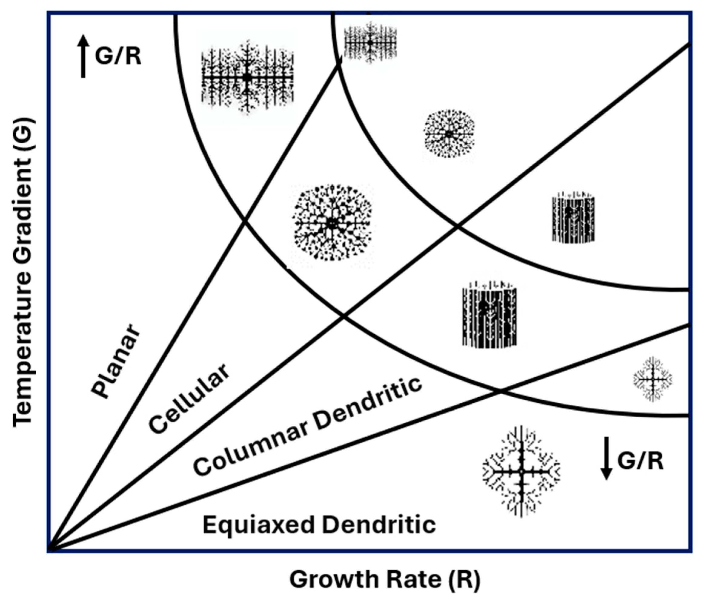
Figure 2.
Preheat Strategies implemented during build; (a) Raster build; (b) Spot melt.

Figure 3.
Scan Strategies implemented during the build; (a) Raster build; (b) Stochastic Spot melt.
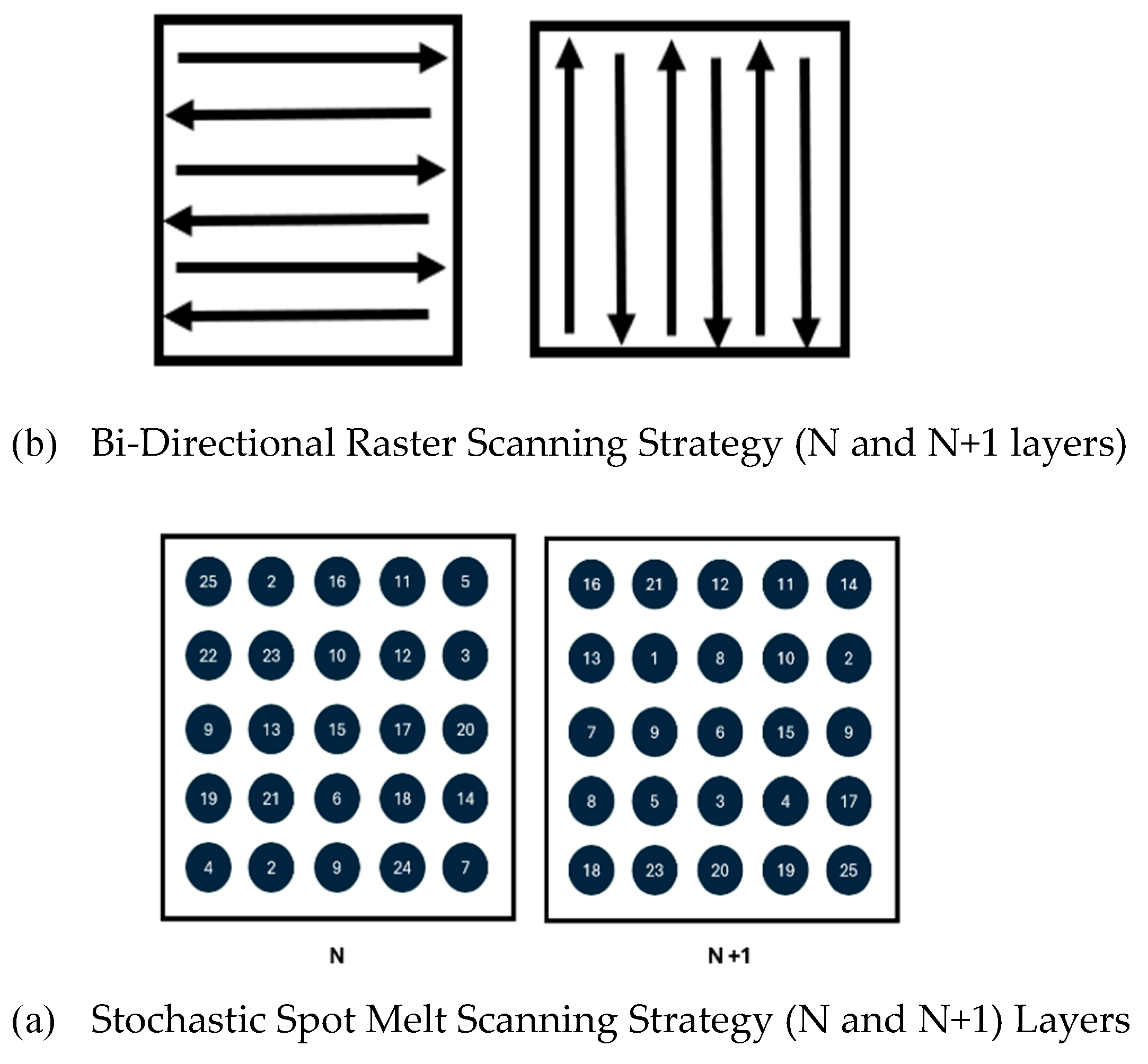
Figure 4.
Build fabrication process for (a) raster build and (b) stochastic spot melt build.
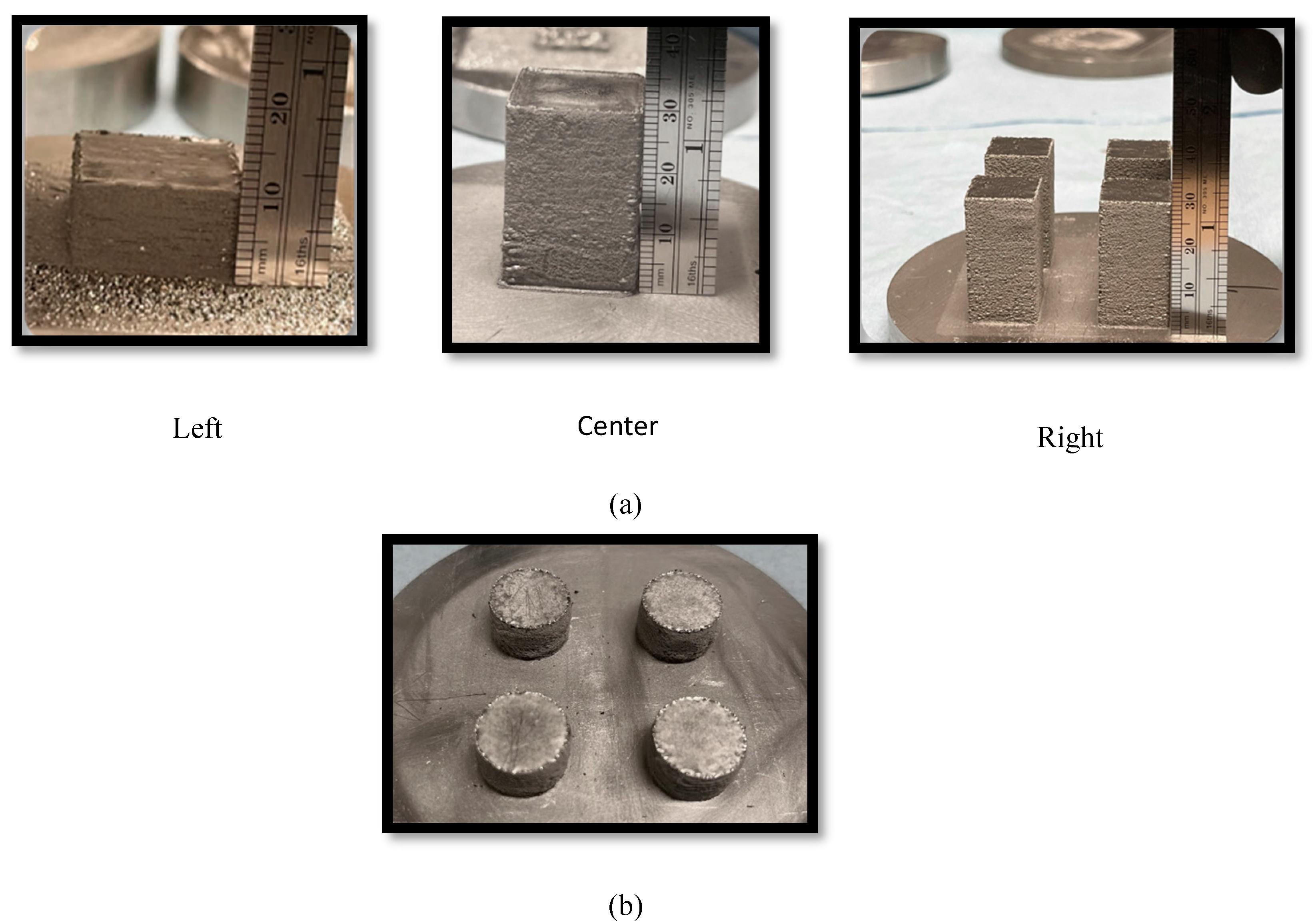
Figure 5.
Scatterplot of Relative Density and Energy Eas for Stochastic Spot Melt scan builds.
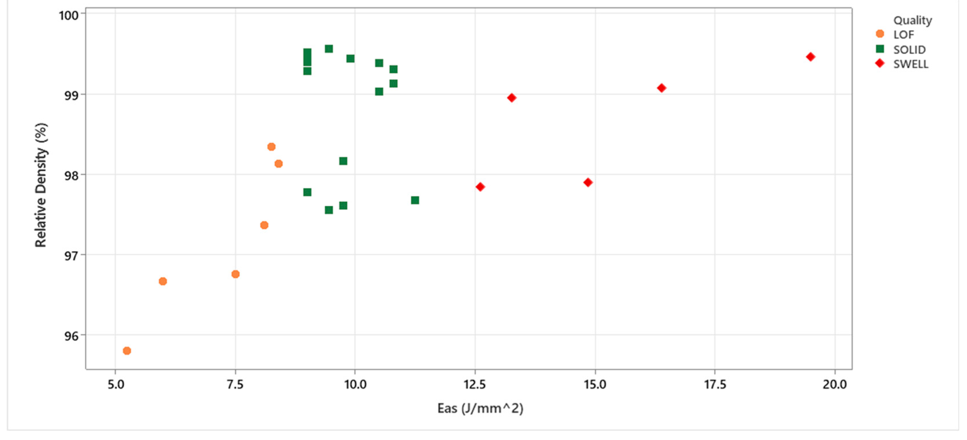
Figure 6.
EBSD Results and pole configuration for Raster Scan Build (a) Top; (b)Bottom of the build specimen in build direction.
Figure 6.
EBSD Results and pole configuration for Raster Scan Build (a) Top; (b)Bottom of the build specimen in build direction.
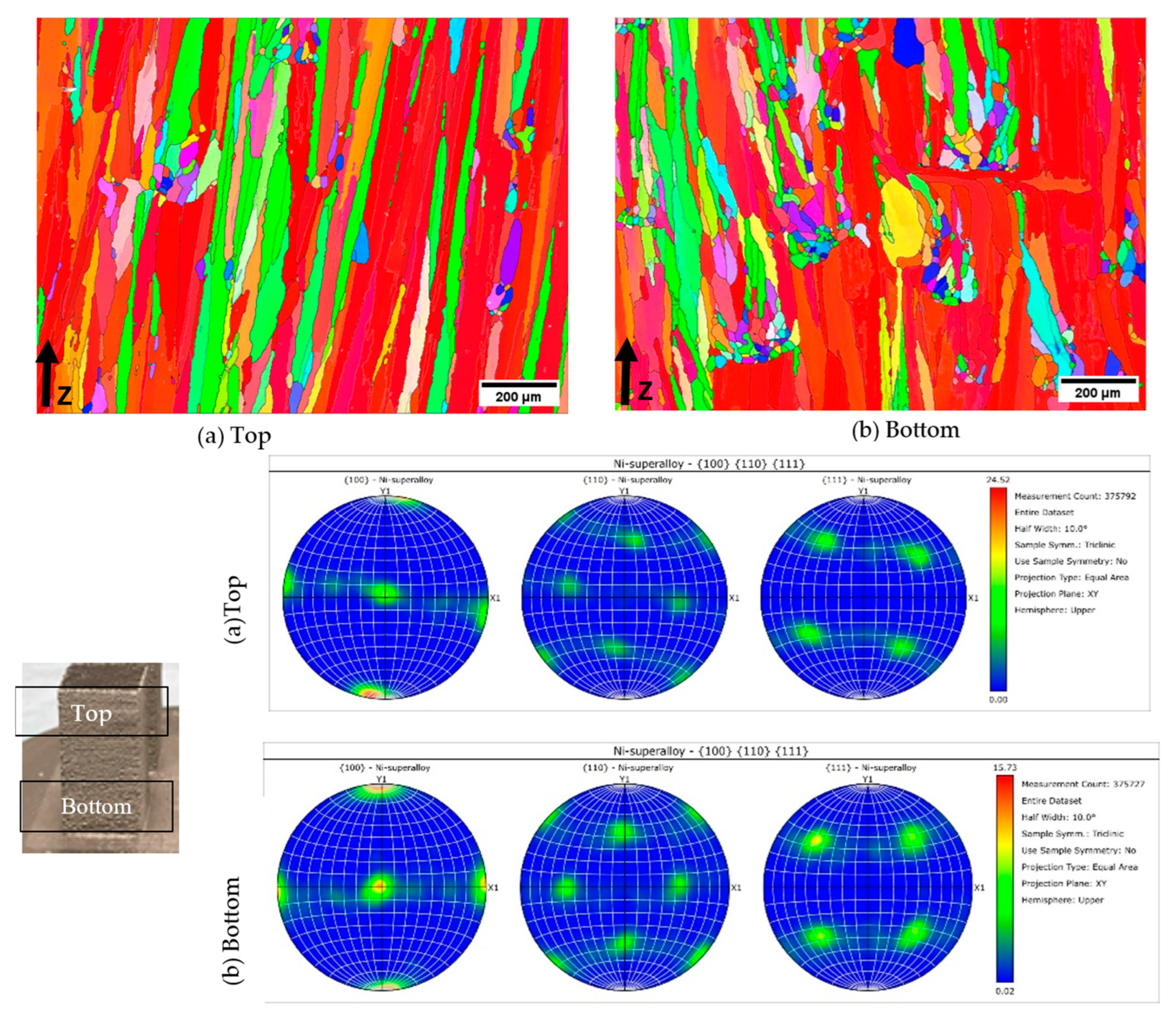
Figure 7.
Schematic diagram illustrating sample direction and assessment method.
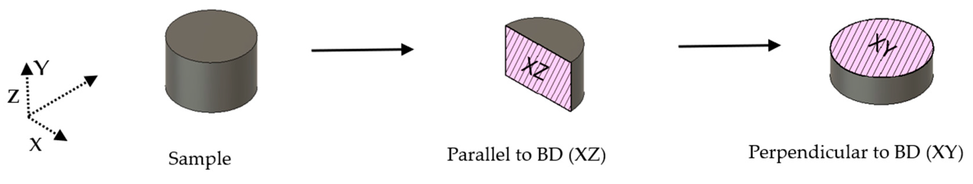
Figure 8.
EBSD results for Spot melt specimens Perpendicular to Build Direction.
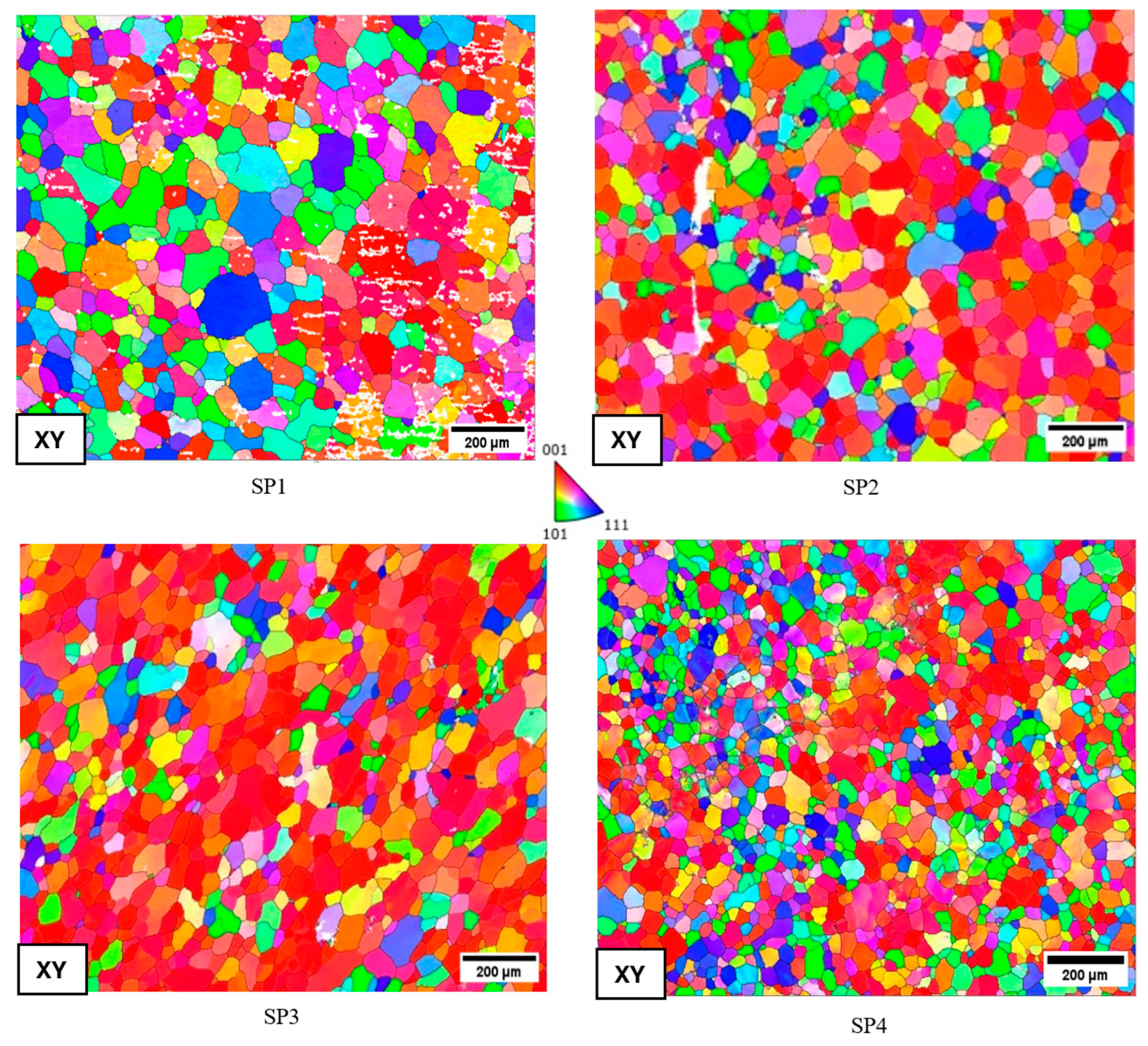
Figure 9.
EBSD results in parallel to build direction for Stochastic spot melt samples.
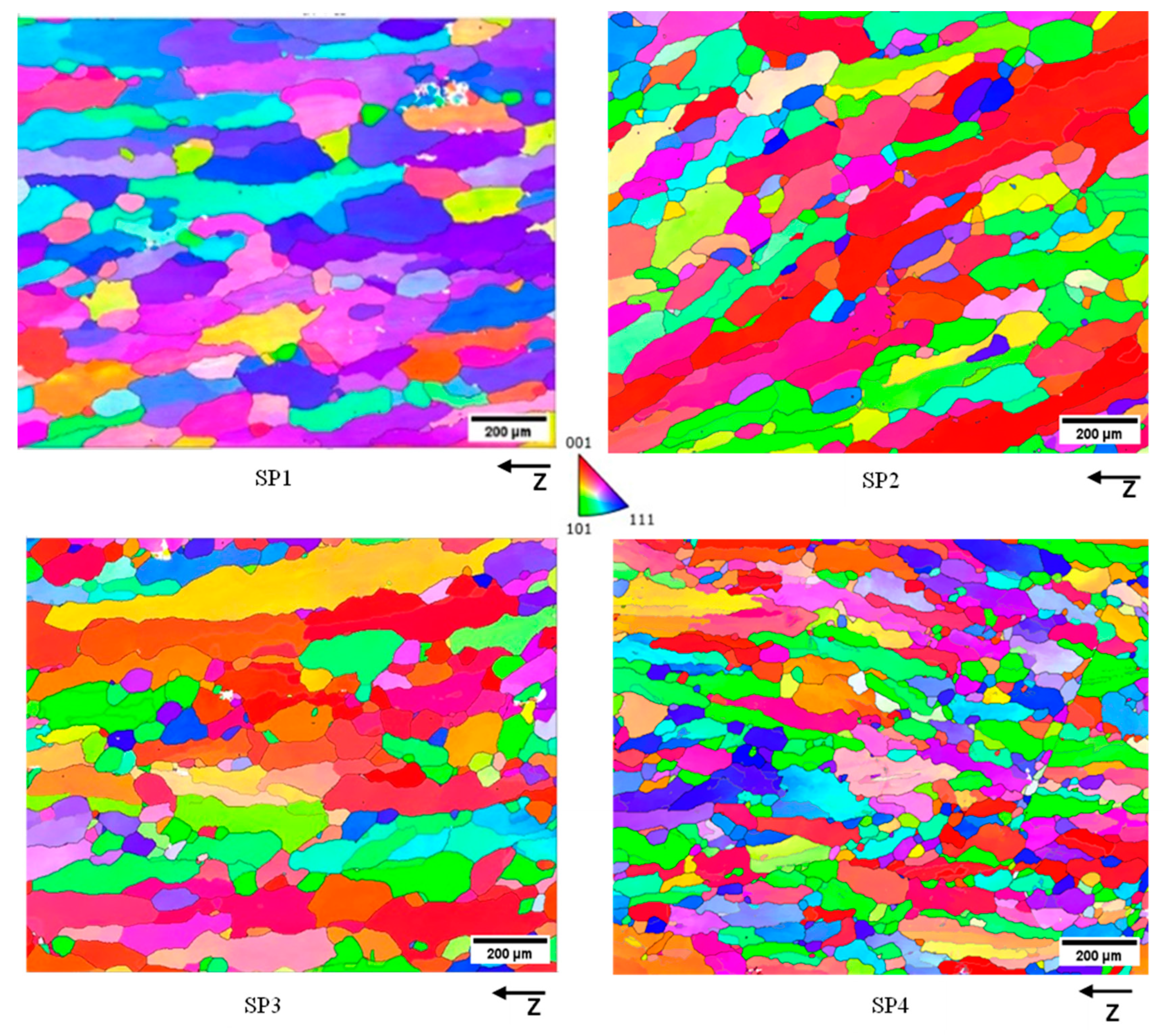
Figure 10.
Pole Configuration of the EBSD samples Parallel build direction.
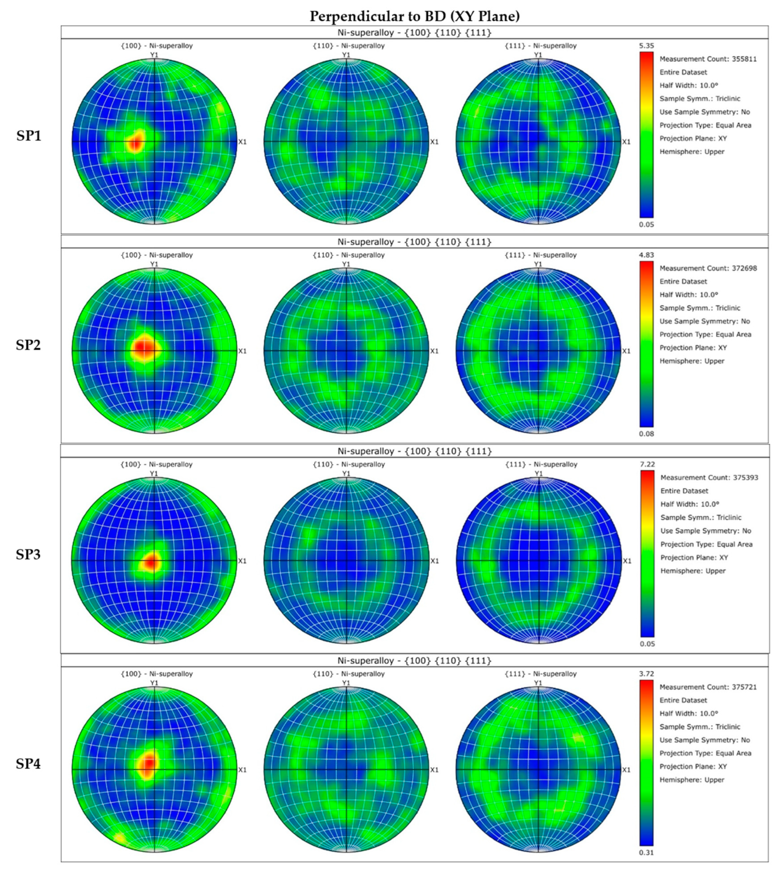
Figure 11.
Pole Configuration of the EBSD samples Parallel build direction.
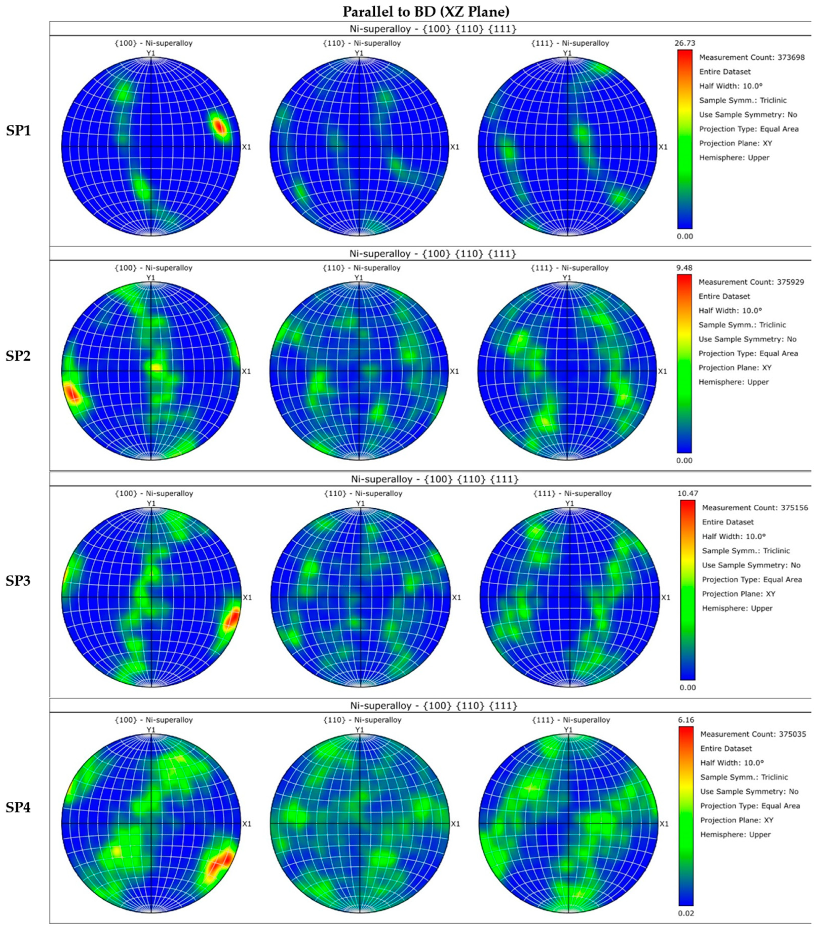
Figure 12.
Vickers microhardness results in the HV1 scale for raster and Stochastic.
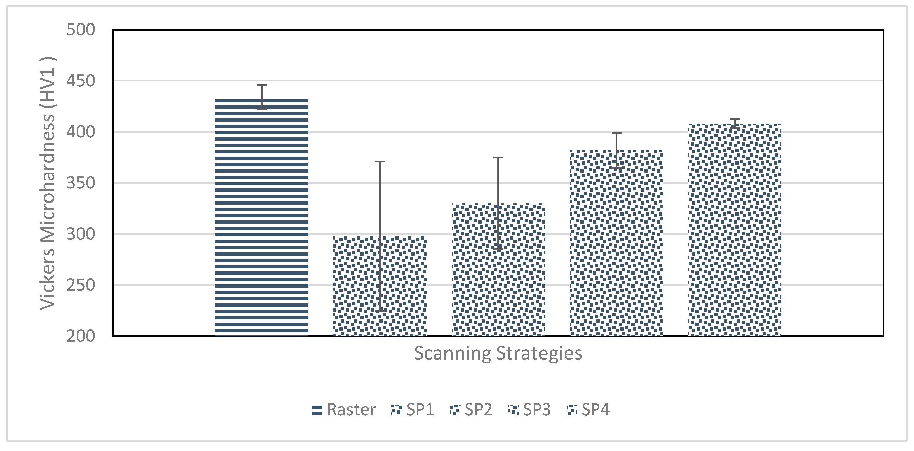

Table 1.
Experimental Parameters for Raster Scan Builds.
| Power (W) | Speed (mm/s) | Ea (J/mm2) | Relative Optical Density | Type |
|---|---|---|---|---|
| 720 | 2400 | 3 | 97.81 | Solid |
| 600 | 2400 | 2.5 | 95.7 | LOF |
| 300 | 1200 | 2.5 | 96.47 | LOF |
| 360 | 1200 | 3 | 98.38 | Solid |
| 300 | 800 | 3.75 | 99.87 | Solid |
Table 2.
EBSD Specimen evaluated for stochastic spot melt.
| Specimen | SP1 | SP2 | SP3 | SP4 |
|---|---|---|---|---|
| Power (Watt) | 720 | 660 | 420 | 360 |
| Spot Dwell(microseconds) | 125 | 125 | 250 | 250 |
| Eas (J/mm2) | 9 | 8.25 | 10.25 | 9 |
| Melt Time (seconds) | 2.21 | 2.21 | 4.42 | 4.42 |
Table 3.
Detailed observations from EBSD results for Raster and Stochastic Spot Melt build.
| Metric (Parallel to Build Direction) | Raster Build | Stochastic Spot Melt Build | ||||
|---|---|---|---|---|---|---|
| Top Section | Bottom Section | SP1 | SP2 | SP3 | SP4 | |
| Grain Count | 425 | 813 | 192 | 308 | 342 | 643 |
| Mean Aspect Ratio | 5.9 | 3.6 | 2.9 | 2.7 | 2.6 | 2.5 |
| Area-weighted Mean Aspect Ratio | 10.9 | 5.6 | 3.5 | 4.0 | 3.9 | 3.5 |
| Min Aspect Ratio | 1.1 | 1.0 | 1.0 | 1.1 | 1.0 | 1.0 |
| Max Aspect Ratio | 36.8 | 36.3 | 9.6 | 9.8 | 9.9 | 12.7 |
| Standard Deviation | 5.4 | 2.9 | 1.6 | 1.5 | 1.5 | 1.5 |
Table 4.
Detailed observations from EBSD results for Raster and Stochastic Spot Melt build.
| Build | Test 1 | Test 2 | Test 3 | Test 4 | Test 5 | Mean | Standard Deviation |
|---|---|---|---|---|---|---|---|
| Raster | 451 | 437 | 431 | 418 | 432 | 434 | 11.9 |
| SP1 | 397 | 266 | 235 | 238 | 352 | 298 | 72.9 |
| SP2 | 395 | 306 | 288 | 304 | 359 | 330 | 44.9 |
| SP3 | 391 | 365 | 359 | 388 | 405 | 382 | 17.1 |
| SP4 | 401 | 412 | 408 | 406 | 412 | 408 | 4.1 |
Disclaimer/Publisher’s Note: The statements, opinions and data contained in all publications are solely those of the individual author(s) and contributor(s) and not of MDPI and/or the editor(s). MDPI and/or the editor(s) disclaim responsibility for any injury to people or property resulting from any ideas, methods, instructions or products referred to in the content. |
© 2024 by the authors. Licensee MDPI, Basel, Switzerland. This article is an open access article distributed under the terms and conditions of the Creative Commons Attribution (CC BY) license (http://creativecommons.org/licenses/by/4.0/).
Copyright: This open access article is published under a Creative Commons CC BY 4.0 license, which permit the free download, distribution, and reuse, provided that the author and preprint are cited in any reuse.


