
Submitted:
20 July 2024
Posted:
22 July 2024
You are already at the latest version
Abstract
A fundamental aspect in the evolution of Time-to-Digital Converters (TDCs) implemented within Field-Programmable Gate Arrays (FPGAs), given the increasing demand for detection channels, is the optimization of resource utilization. This study reviews the principal methodologies employed for implementing low-resource TDCs in FPGAs. It outlines the foundational architectures and interpolation techniques utilized to bolster TDC performances without unduly burdening resource consumption. Low-resource Tapped Delay Line, Vernier Ring Oscillator, and Multi-Phase Shift Counter TDCs, including the use of SerDes, are reviewed. Additionally, novel low-resource architectures are scrutinized, including Counter Gray Oscillator TDCs and interpolation expansions using Voltage-Temperature-Consumption stable IODELAYS. Furthermore, the advantages and limitations of each approach are critically assessed, with particular emphasis on resolution, precision, non-linearities, and, especially, resource utilization. A comprehensive summary table encapsulating existing works on low-resource TDCs is provided, offering a comprehensive overview of the advancements in the field.
Keywords:
Time-to-Digital Converter
; Field Programmable Gate Array
; Low-resource Time-to-Digital Converters
1. Introduction
Time-to-Digital Converters (TDCs), which convert a pulse time duration into a numeric value, are used in various applications where an accurate measurement of time is needed, such as time-based signal processing [1], ASIC testing [2], detection of Trojan infection in ASIC [3], nuclear medicine image with Positron Emission Tomography [4,5,6,7], measurement of the laser flight time in laser ranging [8], fluorescence spectroscopy [9], ultrawideband radio frequency localization [10,11], Laser Imaging Detection and Ranging [12], or experiments of high-energy physics [13,14,15,16], including neutrino telescopes [17,18,19], and accelerator instrumentation [20,21,22].
TDCs can be implemented in both, ASICs and FPGAs. ASICs can provide better performances, especially when there are requirements for high resolution. Nevertheless, FPGAs are less expensive and complex than ASICs, they provide faster development time and the flexibility to adapt the logic to the operation conditions, reducing the development costs and the time-to-market time [23,24,25,26,27]. Furthermore, the remaining FPGA resources can be utilized to process TDC data and interface with the rest of the readout system, which results in higher reliability [28,29,30].
There is an increasing demand for a higher number of TDC channels implemented in FPGAs, which requires low-resource and low-power TDCs. FPGAs are devices designed to operate synchronously, therefore the primary and simplest method for implementing TDCs consists of a simple counter. The resolution of this basic implementation can be extended using various methods, allowing for resolutions significantly finer than the period of the counter clock. To extend the counter’s resolution, the Nutt or interpolation architecture [31] is employed in FPGAs. The counter keeps track of the clock cycles, while an interpolator computes the fractional part within the clock cycle for both the start and stop segments.
The most used low-resource interpolation methods are the Multi-Phase Shift Clock (MPSC) and the Gray Code Oscillator (GCO), while there are also advances to reduce the number of resources used in Tapped Delay Line (TDL) and Vernier Ring Oscillator (VROs) TDCs. A special type of TDC is based on a two-step interpolation, each of the two using different interpolation techniques. Noise-Shaping (NS) TDCs have recently been implemented fully in FPGAs, although the use of resources is still considerable. The advances in low-resource TDCs, with their advantages and drawbacks, are reviewed in this work. Table 1 shows the existing works on low-resource TDCs reviewed in this work. The counter architecture, the simplest method to implement TDCs in FPGAs is presented in Section 3. The main parameters describing TDCs are detailed in Section 2, while Section 4 is dedicated to TDL-TDCs, Section 5 discusses VRO-TDCs, NS-TDCs are analyzed in Section 6, GCO-TDCs are presented in Section 7, MPSC-TDCs are reviewed in Section 8, while Section 9 is dedicated to two-stage conversion TDCs. Finally, a discussion takes place in Section 10, while the conclusions are presented in Section 11.
2. TDC Main Parameters
The performance and characteristics of a TDC are defined by several key parameters. The most important of them include:
- Resolution refers to the smallest detectable time interval or the smallest distinguishable step in time measurement that the TDC can achieve. The smallest resolvable time interval is represented by the Least Significant Bit (LSB) which establishes the resolution of the TDC.
- Dead-time refers to the minimum time interval required between two consecutive events or pulses for accurate detection and measurement. It is the period during which the TDC is temporarily unable to respond to incoming signals due to internal processing, resetting, or recovery time. Dead-time is an inherent characteristic of TDCs and is primarily caused by the time required for data acquisition, signal conditioning, digitization, and internal circuitry operations.
- Precision refers to the repeatability and consistency of time measurements performed by the TDC. It is directly affected by the non-linearities of the TDC.
- Differential Non-linearities (DNL) can be defined as the deviation of a single quantization step from the ideal LSB. It quantifies the step size variation between consecutive output codes. DNL is typically expressed as the difference between the measured step size and the ideal step size (in LSB). The DNL is evaluated by comparing the number of pulses per bin () with the mean value ()
- Integral Non-linearities (INL) describe the greatest deviation of the transfer function of a TDC from the ideal linear relationship. The INL value provides information about the linearity and precision of the TDC’s measurements. It can be determined by performing the following calculation:where represents the input width, denotes the average of the pulse width measurements, and indicates the bin size.
- Range refers to the time intervals that the TDC is capable of accurately measuring. It represents the minimum and maximum values that the TDC can handle within its specified operating conditions.
- Clock Frequency refers to the frequency at which the TDC’s internal clock operates, influencing the resolution and measurement capabilities.
- Calibration is required by some TDCs to compensate for non-linearities and enhance accuracy. Usually, the calibration system increases the use of resources.
- Resources occupancy concerns to the utilization of FPGA resources, such as lookup tables (LUTs), flip-flops (FFs), memory blocks, interconnects, or other FPGA hardware such as SerDes or IOs delays to implement the TDC functionality. The present review is dedicated to TDCs which are implemented with low use of resources.
3. The Basics: The Counter and the Interpolator
The simplest method to implement a TDC in an FPGA is the counter method, where the time interval is measured by counting the number of clock cycles that occur between two events. The resolution of the TDC is determined by the clock frequency. In FPGAs, the frequency is limited to a few hundredths megahertz [32,33], which, in turn, limits the performances of the TDCs. One of the main advantages of this method is that non-linearities are minimal and dependent on the clock jitter. Another advantage is that the TDC’s scale can be extended as needed simply by increasing the counter’s range.
The range of the TDC can be calculated as follows:
Where Range is the maximum measurable time interval, n represents the number of bits in the counter, and is the period of the clock signal. By increasing the number of bits in the counter, the total countable range of the TDC is also increased. For each additional bit added, the TDC’s measurable range is effectively doubled. As shown in Figure 1, the start and end of the pulse input are not properly measured. To enhance the TDC’s resolution, interpolation or the Nutt method is employed. This approach delivers greater resolution. The counter provides a coarse count, while the time intervals before the first counting cycle and after the last one are interpolated with a finer resolution method. The counter keeps track of the clock cycles, while the interpolator computes the fractional part within the clock cycle in both the start and stop signals with respect to the clock edge. In the realm of Field-Programmable Gate Arrays (FPGAs), two primary interpolation methods are employed to implement low-resource TDCs: MPSC and GCO, while other interpolation methods such as TDL and VRO have achieved considerable reduction in the use of resources. Each of these methods will be thoroughly detailed in the subsequent sections.
4. Tapped Delay Line TDCs
The TLD technique relies on a logic buffer delay cell, where the start signal propagates, and the stop signal latches the state of the delay line in a register (See Figure 2). The resolution is determined by the basic delay duration, while the precision is determined by the uniformity of the delay tap. When the rising edge of the master clock signal detects the start or end of a pulse at the input of the TDC, all the FFs in the TDL are frozen and read, enabling a more precise measurement of the time interval [34]. Different alternatives have been explored to implement the TDL in FPGAs. The FPGA routing resources can be used to create the basic delay, used also to implement vernier TDCs [35]. Other elements to implement the TDL are FFs [36] and LUTs [37]. DSP blocks within FPGAs have also been used to implement TDLs [38], while the most widely adopted approach for implementing TDL TDCs is the use of the arithmetic carry propagation primitive [39].
Recent implementations of TDL-TDC using carry lines have achieved picosecond resolution [39,40,41]. However, it is important to note that the arithmetic carry, when implemented in an FPGA, does not exhibit a linear delay behavior. As a result, TDL architectures relying on arithmetic carry methods can suffer from high levels of differential and integral non-linearity errors (DNLs and INLs). These errors manifest as some of the tapped delays do not follow the programmed order, a phenomenon known as "bubble error". Bubble error directly impacts the precision of TDCs and introduces non-linearities into the measurements. Additional variations can occur due to periodic patterns arising from the Complex Logic Block (CLB) structure and the clock distribution tree boundaries within the FPGA. It is essential that the cumulative delay in the chain exceeds the period of the coarse counter clock to ensure accurate time measurements. Implementing TDL-TDCs with carry chains leads to higher system complexity and intensive utilization of FPGA resources. Achieving uniform delays often requires manual routing, which adds additional complexity to the development process. To enhance the intrinsic resolution of the TDL beyond what is limited by the granularity of the basic delay, TDL-TDCs in parallel have been used [42]. By using 125 TDL-TDCs of 323 ps in parallel, a resolution of just 5.8 ps has been achieved [43]. However, the use of several TDCs in parallel considerably increases the use of resources.
TDL-TDCs, in any of its variations, are not Power, Voltage and Temperature (PVT) compensated (one exception is the TDL created with IODELAY primitives), are highly non-linear, which requires calibration and are highly intensive in the utilization of FPGA resources. TDL-TDCs consume high resources when compared with other architectures with higher efficiency [40], nevertheless, recently, some advances have been made in the area of low resources and Parsa et al. have developed a TDL-TDC with reduced resource consumption. Although resolution and precision are high (< 30 ps), both the non-linearities and the number of resources are still considerable, especially the consumption of BRAM blocks [44,45], which is as high as 90 kB per TDC channel. The implementation has been done in an Artix-7 FPGA where DNLs of 2.13 LSBs have been achieved in the first implementation and 1.18 LSBs in the optimized version (INLs of 3.97 and 2.75 LSBs respectively), with consumption of 216 LUTs and 678 FFs in both implementations.
5. Vernier Ring Oscillator TDCs
The Vernier TDC is based on a reference delay line and a delayed signal path, both with slightly different propagation delays [46,47]. By comparing the delayed signal with the reference, the TDC determines the time difference between the events through an interpolation-like process, providing enhanced resolution beyond the clock resolution. A subtype of vernier TDCs, the Vernier Ring Oscillator (VRO)-TDC can be implemented in a very efficient manner, reducing the number of resources used [48] (see basic scheme in Figure 3). The VRO-TDC is based on two external oscillators of different frequencies [49]. The oscillators are controlled with the start and stop signals of the pulse which duration has to be measured. The highest frequency oscillator (with period) is initialized by the start signal and the lower frequency oscillator (with period) is initialized by the stop signal. After N cycles, both oscillators will be aligned and will be the time difference between start and stop signals: . The TDC accuracy is determined by the difference between the periods of the two oscillators. The dead-time is sensibly high as the TDC has to wait until both clocks are aligned. Cui et al. have implemented low-resource VRO-TDCs with similar resolutions (< 30 ps) to the one achieved by Parsa et al. with TDL-TDCs, with a higher number of registers but with no use of BRAM blocks and better non-linearities [50]. Higher linearity has been achieved with this type of TDC but with higher consumption of resources [51] (172 LUTs and 986 FFs versus 104 LUTs and 319 FFs of the first implementation).
6. Noise-Shaping TDCs
TDCs have been extensively used to measure the time delay between two repetitive digital signals (or clocks) with high precision. The primary drawback of this technique is its inability to measure a single-event input. An additional limitation arises from the requirement for certain analog components, such as an integrator and a comparator, which complicates the full implementation in FPGAs [52]. Recently, advancements have been made to overcome these challenges. A sophisticated type of TDC, specifically a high-order continuous-time multi-stage noise shaping (MASH) 16 TDC, has been successfully integrated entirely within an FPGA. This was achieved by utilizing a Gated Switched-Ring Oscillator (GSRO) [53]. This integration represents a significant milestone in the field. Despite achieving a remarkably high resolution of 0.18 ps, the implementation by Khaki et al. still involves substantial resource consumption. While only 311 registers are used, the requirement for 5 phase-locked loops (PLLs) and, notably, 2 Mb of memory, precludes this type of TDC from being classified as low-resource at this stage. The progress in this area is promising, but further optimization is necessary to reduce resource utilization and enhance the feasibility of widespread low-resource FPGA implementation.
7. Gray Code Oscillators TDC
Wu et al. have proposed an innovative TDC architecture base in a free-running gray code oscillator [22]. Instead of using a synchronous counter, a combinational counter is implemented, running much faster, and thus increasing the resolution, reducing the resource utilization and power consumption, while providing high scalability and portability. The gray code needs to be used, as being combinational and not having the delay time controlled, only one-bit transition propagates back to the input, so glitches are not generated, which would appear if another type of code were used. The implementation of the gray counter consumes very low resources which is compensated by the necessary logic to improve the linearity via calibration. The drawbacks of this architecture are that the TDC bins have high non-linearities and that, as is the case with the previous solutions, is not PVT compensated. Upgrades on the architecture have been done to improve the non-lineareties [54] and the resolution [12]. The latest improvement on this architecture, achieved by Wang et al. has reached resolution and precision below 40 picoseconds, nevertheless, the use of resources is still high, requiring 437 LUTs, 368 FFs, and 54 kB of RAM per channel in a Virtex-7 FPGA [55].
8. Multi-Phase Shift Clock TDC
The MPSC method utilizes several clocks with the same frequency but different phases, oversampling the TDC input (See Figure 4). Each clock monitors the TDC line, latching the status at the rising edge of the clock, thereby multiplying the resolution achievable by a single clock (See Figure 5). It is resource-efficient, enabling hundreds of channels in one FPGA. The resolution is increased by the number of phases used. The MPSC-TDCs usually have a reduced DNL, as the feature is intrinsic to the architecture and related to the jitter of the clocks. The main drawbacks are the limited number of clock lines the FPGA can support, the fan-out, and, especially, the skew on the lines from the input signal to the FFs that could be much bigger than the requested resolution. If the time path between two consecutive phases is bigger than the LSB, the signal of that specific phase will be sampled at the following clock edge, then the final timestamp will not match with the real measure. This limits the resolution that can be achieved with MPSC-TDCs.
One of the first implementations of this type of TDC was done by Fries et al. [56], which achieved a resolution of 1400 ps and a DNL of 0.5 LSB. A higher resolution, 138 ps, was obtained by Yonggang et al. [57], who used 8 clock phases. Balla et al. developed an MPSC-TDC [58] with four phases to obtain an LSB of 625 ps and a precision of 255 ps. The total number of LUTs and registers was 68 and 274 respectively. The number of registers included a buffer for 32 measurements (40 bytes in total), although the TDC did not compute the arrival time, which would have increased the consumption of resources. The linearity of the TDC was high, DNL of 0.05 LSBs and INL of 0.05 LSBs. A TDC with 16 phases was implemented by Büchele et al. [59] obtaining a resolution of 160 ps and a precision of 64 ps. The number of LUTs consumed by the TDC channel in a Virtex-5 FPGA was 125, while the number of registers was 198. Suwada et al. [60] and Li et al. [61] have implemented 1000 ps resolution TDCs in Spartan-6 FPGAs. Sano et al. have implemented TDCs with a resolution of 280 ps in a Kintex-7 FPGA [62] and of 780 ps in an IGLOO-2 FPGA [63], in the last case for higher tolerance to irradiation. Jia et al. have achieved a resolution of 138 ps in an Artix-7 FPGA by using a clock of 300 MHz and 24 different phases [64]. The TDCs implemented by Lusardi et al. [65] have achieved a relatively high resolution with very low resources. 156.25 ps of resolution and 93 ps of precision are achieved with only 295 LUTs and 446 registers. An implementation of the same architecture with a lower resolution (625 ps) achieved better non-linearities (DNL 0.045 LSBs and INL of the same value) with a lower resource consumption (212 LUTs and 336 FFs).

Table 1.
Resource utilization comparison. The resource consumption of state-of-the-art low-resource TDCs is shown. For each of the works is presented the resolution, precision, non-linearities, and resource consumption. The works are organized by the technology used in the implementation of the TDC.
| Work | Res. (ps) | Pre. (ps) | DNL/INL(LSB) | LUTs | FFs | Primitive | BRAM (kB) | FPGA |
|---|---|---|---|---|---|---|---|---|
| NS | ||||||||
| Kha-21[53] | 0.18 | NR | NR/NR | NR | 311 | 5 PLL | 2000 | Stratix-IV |
| TDL | ||||||||
| Choi-21[40] | 4.88 | 8.03 | 0.51/0.51 | 2962 | 4157 | 0 | 0 | Artix-7 |
| Pars-21[44] | 22.2 | 26.04 | 2.13/3.97 | 216 | 678 | 0 | 90 | Artix-7 |
| Pars-22[45] | 22.1 | 22.35 | 1.18/2.75 | 216 | 678 | 0 | 90 | Artix-7 |
| VRO | ||||||||
| Cui-17[50] | [23,37] | [32,39] | 0.8/1.7 | 104 | 319 | 0 | 0 | Virtex-6 |
| Cui-20[51] | 24.5 | 28 | 0.45/0.85 | 172 | 986 | 0 | 0 | Virtex-6 |
| GCO | ||||||||
| Wu-19[22] | 256 | 160 | 1.25/NR | NR | NR | 0 | NR | Kintex-7 |
| Mach-20[54] | 380.9 | 290 | 0.76/0.71 | NR | NR | 0 | NR | Virtex-7 |
| Arau-21[12] | 69 | 54.99 | 1.76/1.5 | NR | NR | 0 | NR | Ultrascale+ |
| Wang-23[55] | 20.97 | 17.11 | 0.087/0.224 | 455 | 368 | 0 | 54 | Ultrascale+ |
| Wang-23[55] | 36.01 | 27.37 | 0.102/0.262 | 453 | 367 | 0 | 54 | Ultrascale |
| Wang-23[55] | 34.84 | 32.33 | 0.078/0.203 | 437 | 368 | 0 | 54 | Virtex-7 |
| Wang-23[55] | 256.41 | N/R | 0.65/3.1 | 380 | 333 | 0 | 54 | Virtex-7 |
| MPSC | ||||||||
| Frie-02[56] | 1400 | 750 | 0.4/NR | NR | NR | 0 | 0 | Virtex-5 |
| Buch-12[59] | 160 | 64 | 0.4/NR | 125 | 198 | 0 | 0 | Virtex-5 |
| Wang-13[57] | 138 | NR | 0.29/NR | NR | NR | 0 | 0 | Virtex-5 |
| Ball-14[58] | 625 | 255 | 0.05/0.05 | 68 | 274 | 0 | 0 | Virtex-5 |
| Suwa-15[60] | 1000 | 500 | 0.52/0.39 | NR | NR | 0 | 0 | Spartan-6 |
| Sano-16[62] | 280 | NR | 0.28/0.3 | NR | NR | 0 | 0 | Kintex-7 |
| Sano-17[63] | 780 | 350 | 0.53/2.8 | NR | NR | 0 | 0 | IGLOO-2 |
| Li-17[61] | 1000 | 430 | NR/NR | NR | NR | 0 | 0 | Spartan-6 |
| Jia-18[64] | 138 | 73.6 | NR/NR | NR | NR | 0 | 0 | Artix-7 |
| Lusa-23[65] | 156.25 | 93 | 0.23/0.26 | 295 | 446 | 0 | 0 | Artix-7 |
| Lusa-23[65] | 312.5 | 93 | 0.26/0.2 | 238 | 431 | 0 | 0 | Artix-7 |
| Lusa-23[65] | 625 | 255.5 | 0.045/0.045 | 212 | 336 | 0 | 0 | Artix-7 |
| MPSC SerDes | ||||||||
| Bogd-05[66] | 1200 | 1200 | 0.17/NR | NR | NR | 1 SER | 0 | Stratix |
| Calv-21[18] | 1000 | NR | 0.03/0.12 | NR | NR | 1 SER | 0 | Kintex-7 |
| Kong-23[67] | 100 | 169 | NR/NR | NR | NR | 1 SER | 0 | Kintex-7 |
| Xian-14[68] | 156 | 56 | 0.32/1 | 109 | 238 | 2 SER | 0 | Artix-7 |
| Bai-17[69] | 803 | 229 | 0.05/NR | 30 | 42 | 2 SER 1 IOD | 0 | Artix-7 |
| Arpi-10[7] | 321.5 | 56 | 0.3/0.65 | NR | NR | 4 SER 4 IOD | 0 | Virtex-4 |
| Imre-10[6] | 312 | NR | 0.6/NR | NR | NR | 4 SER 4 IOD | 0 | Virtex-4 |
| Fino-24[70] | 100 | 42 | 0.35/NR | NR | NR | 4 SER 3 IOD | 0 | Artix-7 |
| Two-stage | ||||||||
| Dong-20[71] | 78.13 | 35 | 0.8/0.94 | 199 | 347 | 1 SER 1 IOD | 0 | Kintex-7 |
| Wang-24[72] | 10.05 | 19.81 | 2.85/13.61 | 293 | 385 | 0 | 0 | Virtex-7 |
| Wang-24[72] | 4.57 | 22.88 | 4.36/18.26 | 440 | 570 | 0 | 0 | Ultrascale |
| Real-24[73] | 415.84 | 186 | 0.2/0.15 | 102 | 115 | 1 IOD | 0 | Artix-7 |
8.1. SerDes TDC
A variant of the MPSC-TDC is based on the SerDes, short for Serializer/Deserializer. The SerDes plays a crucial role within an FPGA by converting a high-speed serial data stream into parallel data for reception purposes. The SerDes block can be employed to implement the oversampling method, making it possible to create 4 sampling phases with a single SerDes. Since the SerDes are integrated hardware components connected to the I/O, they occupy minimal FPGA resources. By multiplexing several SerDes is possible to increase the resolution, as it is equivalent to increasing the number of phases.
8.1.1. One- TDC
Several TDCs have been implemented with one SerDes. A TDC with a resolution of 1.2 ns using a Stratix FPGA [66] has been created by Fries et al. The jitter in the clock driven by the PLL is specified to be under 200 ps, resulting in a DNL of less than 200 ps. A TDC with a 1 ns resolution [18] using a Kintex-7 FPGA was implemented by Calvo et al., with DNLs of 0.03 LSBs and INLs of 0.12 LSBs. A higher resolution, 100 ps, has been achieved by Kong et al. [67]. The precision achieved is 169 ps, and it has been obtained in a Kintex-7 by using the SerDes to read 10 GBPS signals, which generates a 32-bit array that is needed to identify the rise and fall edges inside. The number of transceivers of 10 GBPS is limited in the FPGAs, therefore the number of TDC channels that can be implemented using this type of TDC is also limited, and cannot be used in all the inputs of the FPGA as is the case with the usual SerDes.
8.1.2. Two-SerDes TDC
A TDC with a resolution of 156 ps has been proposed by Xiang et al. [68]. The TDC was implemented with two complementary SerDes working at 800 MHz and with 8 different phases separated 45°. The resolution obtained was of 56 ps, the INL of 1 LSB, and the DNL of 0.36 LSBs. The resource usage was of only 109 LUTs and 238 registers in addition to the two SerDes, implemented in an ARTIX-7 FPGA. Bai et al. [69], by using two SerDes and one IODELAY primitive have achieved a resolution of 803 ps and a precision of 229 ps using only 30 LUTs and 42 FFs. The DNL was also very low (0.05 LSBs).
8.1.3. Four-SerDes TDC
Four SerDes acquiring in parallel, with the TDC input delayed one quarter of the SerDes acquisition period have been used to increase even more the resolution, which would be the equivalent of an MPSC-TDC with 16 phases. The TDC developed by Arpin et al. [7] achieved a resolution of 321 ps in a Virtex-4, with a precision of 56 ps. The DNL was 0.3 LSBs and the INL of 1 LSB. A similar resolution was obtained by Imrem et al., also using a Virtex-4. In this case, the DNLs were slightly higher (0.6 LSB). The latest TDC implementation based on this architecture has a resolution of 100 ps. This TDC has been implemented in a Kintex-7 FPGA using the SerDes working with a 625 MHz clock, which gives a total resolution of 42 ps [70]. In order to achieve a higher resolution, four SerDes TDCs are used in parallel, the three last TDCs acquiring the signal delayed 100, 200, and 300 ps. The delays between the TDC subsections were achieved utilizing the IODELAY primitive which allows a granularity in the delays of 39 ps. The main problem related to the use of the IODELAYs is that the granular delay provided by Xilinx is only an average, existing high difference between the delay bins. This leads to high non-linearities, which are not reported in this work. The granularity of the IODELAY decreases in the new families where it is expected that this architecture will increase the linearity. In any case, the main drawback of this architecture is the number of SerDes available in an FPGA, which is one per IO pin, so the use of 4 SerDes limits the number of TDCs that can be implemented to one quarter of the FPGA inputs.
9. Two-Stage Conversion TDC
The use of two interpolation methods in TDCs has been studied as it can increase the resolution while the resources are kept low. Dong et al. [71] have designed a TDC based on SerDes that increases the resolution with an additional TDL. The resolution obtained is 78.13 ps and the precision 35 ps, while, in addition to the SerDes, 199 LUTs and 347 registers are used. The DNL and INL instead are somewhere high, 0.8 and 0.94 LSBs respectively. Real et al. [73] have implemented an MPSC-TDC with four phases that has been expanded with a one-tap delay by using the IODELAYs of Artix-7. The resolution achieved is 416 ps and the precision is 186 ps. The non-linearities are low (DNL 0.2 and INL 0.15 LSB) while the use of resources is quite contained: 102 LUTs and 115 registers. A significant advantage of this architecture, in addition to the low resources, is that the TDC is PVT-controlled. An additional architecture based on two interpolation steps is the one developed by Wang et al. [72], which uses as first interpolator a GCO-TDC and expands it with a TDL of CARRY4s. The resolution achieved in a Virtex-7 is 10 ps with a precision of 19.81 ps. The DNLs and INLs are high, 2.85 and 13.61 LSBs respectively. The resource consumption is 293 LUTs and 385 registers. A drawback of this implementation is that is not PVT compensated, as happens with both, the TDL based on CARRY4 and the GCO TDCs.
10. Discussion
The TDL-TDCs provided the highest precision but their main drawback is that resource consumption is not as reduced as with other architectures. This can be explained by the number of registers needed to latch the TDL. They also present high non-linearities, which requires calibration of the TDC bins. Additionally, the delays are not PVT compensated. An exception to the latest is if the IODELAY is used, however in this case the number of taps is limited by the IOs of the FPGA. VRO-TDCs have similar characteristics to TDL-TDCs, with a somewhat higher use of resources but with lower non-linearities. NS TDCs have been recently implemented completely, in particular a MASH TDC, however, the consumption of resources should still be improved. The GCO TDCs are a novel architecture that provides high resolution and precision, with also low non-linearities, with moderate use of resources. MPSC-TDCs are the most low-resource effective technology, with generally low non-linearities and also moderate resolution and precision. When the SerDes of the FPGA are used, the resource consumption can be reduced even more. Some combinations of interpolators achieve high resolution while the use of resources is kept at a minimum. Especially promising is the use of IODELAYs as the second interpolator, as it allows an increase of the resolution by tapped delays which are PVT compensated. This feature is expected to improve performances in the latest version of FPGAs with the same consumption of resources, as both the granularity of the delay taps and the operation frequency are greater. The integration of the IODELAY architecture with an MPSC-TDC implemented using SerDes holds promising prospects for high efficiency, primarily due to the utilization of specific hardware resources rather than FPGA logic. This approach capitalizes on the strengths of both technologies to achieve optimal performance while conserving resources. This study has exhaustively examined the principal methods for implementing TDCs in FPGAs, elucidating their respective advantages and drawbacks. These findings have been succinctly summarized in Table 2, providing a convenient reference for comparing and contrasting the various approaches.
11. Conclusions
There is a growing need for TDC channels implemented in FPGAs. This work has reviewed the heterogeneous methods to implement low-resource TDCs critically evaluating the benefits and drawbacks of each approach, focusing on factors such as resolution, accuracy, non-linearities, and particularly, resource utilization. By critically evaluating each approach, this research furnishes a comprehensive overview of the existing studies on low-resource TDCs. Through this, it offers valuable insights into the progression of low-resource TDCs, thereby offering a comprehensive overview of progress in the field.
Acknowledgments
The authors acknowledge the financial support of the Ministerio de Ciencia e Innovación for PID2021-124591NB-C41 and PDC2023-145913-I00 funded by MCIN/AEI/10.13039/501100011033 and by “ERDF A way of making Europe”, for ASFAE/2022/014, ASFAE/2022 /023 and AST22_6.2, with funding from the EU NextGenerationEU (PRTR-C17.I01), PDC2023-145913-I00, CSIC-INFRA23013, Generalitat Valenciana for CIDEGENT/2018/034, /2019/043, /2020/049, /2021/23, for CIDEIG/2023/20 and for GRISOLIAP/2021/192 and EU for MSC/101025085, Spain;
References
- Roberts, G.W.; Ali-Bakhshian, M. A Brief Introduction to Time-to-Digital and Digital-to-Time Converters. IEEE Transactions on Circuits and Systems II: Express Briefs 2010, 57, 153–157. [Google Scholar] [CrossRef]
- Qiu, L.; Zheng, Y.; Siek, L. Multichannel Time Skew Calibration for Time-Interleaved ADCs Using Clock Signal. Circuits, Systems, and Signal Processing 2015, 35. [Google Scholar] [CrossRef]
- Guimarães, L.A. Testing Techniques for Detection of Hardware Trojans in Integrated Circuits of Trusted Systems. PhD thesis, Micro and nanotechnologies/Microelectronics, Université Grenoble Alpes, 2018.
- Aguilar, A.; et al. Time of flight measurements based on FPGA using a breast dedicated PET. Journal of Instrumentation 2014, 9, C05012. [Google Scholar] [CrossRef]
- Moses, W. Time of flight in PET revisited. IEEE Transactions on Nuclear Science 2003, 50, 1325–1330. [Google Scholar] [CrossRef]
- Imrek, J.; et al. FPGA based TDC using Virtex-4 ISERDES blocks. IEEE Nuclear Science Symposium and Medical Imaging Conference; 2010; pp. 1413–1415. [Google Scholar] [CrossRef]
- Arpin, L.; et al. A Sub-Nanosecond Time Interval Detection System Using FPGA Embedded I/O Resources. IEEE Transactions on Nuclear Science 2010, 57, 519–524. [Google Scholar] [CrossRef]
- Song, B.; Zheng, W. The Research of Precision Timing Measurement in Application of TDC GP2 in Laser Ranging. 2013, 8905, 890523. [Google Scholar] [CrossRef]
- Tyndall, D.; Rae, B.R.; Li, D.D.U.; et al. A High-Throughput Time-Resolved Mini-Silicon Photomultiplier With Embedded Fluorescence Lifetime Estimation in 0.13 um CMOS. IEEE transactions on biomedical circuits and systems 2012, 6, 562–70. [Google Scholar] [CrossRef] [PubMed]
- Zwirello, L.; Schipper, T.; Jalilvand, M.; Zwick, T. Realization Limits of Impulse-Based Localization System for Large-Scale Indoor Applications. IEEE Transactions on Instrumentation and Measurement 2015, 64, 39–51. [Google Scholar] [CrossRef]
- De Angelis, A.; Dwivedi, S.; Händel, P. Characterization of a Flexible UWB Sensor for Indoor Localization. IEEE Transactions on Instrumentation and Measurement 2013, 62, 905–913. [Google Scholar] [CrossRef]
- Araújo, S.; Machado, R.; Cabral, J. Double-sampling Gray TDC with a ROS Interface for a LiDAR System. 2021 7th International Conference on Event-Based Control, Communication, and Signal Processing (EBCCSP); 2021; pp. 1–8. [Google Scholar] [CrossRef]
- Arai, Y. TDC architecture study for the ATLAS muon tracker 1997.
- Carrió, F. Upgrading the ATLAS Tile Calorimeter Electronics. EPJ Web of Conferences 2013, 60, 20057. [Google Scholar] [CrossRef]
- Bifulco, P.; Izzo, V.; Mastroianni, S.; et al. A fully-digital and fully -synthetizable TDC for high energy physics experiments. Second International Conference on Event-based Control, Communication, and Signal Processing (EBCCSP); 2016; pp. 1–4. [Google Scholar] [CrossRef]
- Balla, A.; Beretta, M.; Ciambrone, P.; et al. Low resource FPGA-based Time to Digital Converter. IEEE Transaction on Instrumentation and Measurement 2012. [Google Scholar]
- Hazen, E.; et al. The DUMAND-II digitizer. 23rd International Cosmic Ray Conference Proceedings, Calgary, Canada, July 19-30, 1993, 1993.
- Aiello, S.; et al. Architecture and performance of the KM3NeT front-end firmware. J. Astron. Telesc. Instrum. Syst. 2021, 7, 016001. [Google Scholar] [CrossRef]
- Aiello, S.; et al. KM3NeT front-end and readout electronics system: hardware, firmware and software. J. Astron. Telesc. Instrum. Syst. 2019, arXiv:astro-ph.IM/1907.06453]5, 046001. [Google Scholar] [CrossRef]
- Portaluppi, D.; Pasquinelli, K.; Cusini, I.; Zappa, F. Multi-Channel FPGA Time-to-Digital Converter With 10 ps Bin and 40 ps FWHM. IEEE Transactions on Instrumentation and Measurement 2022, 71, 1–9. [Google Scholar] [CrossRef]
- Yuan, Q.; Zhang, B.; Wu, J.; Zaghloul, M.E. A high resolution time-to-digital converter on FPGA for Time-Correlated Single Photon Counting. 2012 IEEE 55th International Midwest Symposium on Circuits and Systems (MWSCAS); 2012; pp. 900–903. [Google Scholar] [CrossRef]
- Wu, J.; Xu, J. A Novel TDC Scheme: Combinatorial Gray Code Oscillator Based TDC for Low Power and Low Resource Usage Applications. 2019 5th International Conference on Event-Based Control, Communication, and Signal Processing (EBCCSP); 2019; pp. 1–7. [Google Scholar] [CrossRef]
- Tontini, A.; Gasparini, L.; Pancheri, L.; Passerone, R. Design and Characterization of a Low-Cost FPGA-Based TDC. IEEE Transactions on Nuclear Science 2018, 65, 680–690. [Google Scholar] [CrossRef]
- Caponio, F.; Abba, A.; Lusardi, N.; Geraci, A. A high-precision wave union TDC implementation in FPGA. 2013 IEEE Nuclear Science Symposium and Medical Imaging Conference (2013 NSS/MIC); IEEE, 2013; pp. 1–4. [Google Scholar]
- Favi, C.; Charbon, E. A 17ps time-to-digital converter implemented in 65nm FPGA technology. In Proceedings of the ACM/SIGDA international symposium on Field programmable gate arrays; 2009; pp. 113–120. [Google Scholar]
- Lusardi, N.; Palmucci, A.; Geraci, A. Fully-migratable TDC architecture for FPGA devices. 2016 IEEE Nuclear Science Symposium, Medical Imaging Conference and Room-Temperature Semiconductor Detector Workshop (NSS/MIC/RTSD); IEEE, 2016; pp. 1–3. [Google Scholar]
- Lusardi, N.; Garzetti, F.; Cibin, M.; Sury, R.; Geraci, A. Hardware and software co-design of a system-on-chip for real-time bidirectional transfer and processing of data from a time-to-digital converter. 2017 IEEE Nuclear Science Symposium and Medical Imaging Conference (NSS/MIC); IEEE, 2017; pp. 1–6. [Google Scholar]
- Abbas, M.; Khalil, K. A 23ps resolution Time-to-Digital converter implemented on low-cost FPGA platform. 2015 International Symposium on Signals, Circuits and Systems (ISSCS); 2015; pp. 1–4. [Google Scholar] [CrossRef]
- Wang, H.; Zhang, M.; Yao, Q. A new realization of time-to-digital converters based on FPGA internal routing resources. IEEE Transactions on Ultrasonics, Ferroelectrics, and Frequency Control 2013, 60, 1787–1795. [Google Scholar] [CrossRef]
- Pan, W.; Gong, G.; Li, J. A 20-ps Time-to-Digital Converter (TDC) Implemented in Field-Programmable Gate Array (FPGA) with Automatic Temperature Correction. IEEE Transactions on Nuclear Science 2014, 61, 1468–1473. [Google Scholar] [CrossRef]
- Nutt, R. Digital time intervalometer. Review of scientific instruments 1968, 39, 1342–1345. [Google Scholar] [CrossRef]
- Liu, C.; Wang, Y. A 128-Channel, 710 M Samples/Second, and Less Than 10 ps RMS Resolution Time-to-Digital Converter Implemented in a Kintex-7 FPGA. IEEE Transactions on Nuclear Science 2015, 62, 773–783. [Google Scholar] [CrossRef]
- Machado, R.; Cabral, J.; Alves, F.S. Recent Developments and Challenges in FPGA-Based Time-to-Digital Converters. IEEE Transactions on Instrumentation and Measurement 2019, 68, 4205–4221. [Google Scholar] [CrossRef]
- Andaloussi, M.; Boukadoum, M.; Aboulhamid, E. A novel time-to-digital converter with 150 ps time resolution and 2.5 ns pulse-pair resolution. The 14th International Conference on Microelectronics; 2002; pp. 123–126. [Google Scholar] [CrossRef]
- Wang, H.; Zhang, M.; Yao, Q. A new realization of time-to-digital converters based on FPGA internal routing resources. IEEE Transactions on Ultrasonics, Ferroelectrics, and Frequency Control 2013, 60, 1787–1795. [Google Scholar] [CrossRef] [PubMed]
- Chen, Y.C.; Chang, H.C.; Chen, H. Two-Dimensional Multiply-Accumulator for Classification of Neural Signals. IEEE Access 2018, 6, 19714–19725. [Google Scholar] [CrossRef]
- Weber, A.A. Development of readout electronics for the RICH detector in the HADES and CBM experiments - HADES RICH upgrade, mRICH detector construction and analysis -. PhD thesis, Giessen U., 2021. [CrossRef]
- Kwiatkowski, P. Employing FPGA DSP blocks for time-to-digital conversion. Metrology and Measurement Systems 2019, vol. 26, 631–643. [Google Scholar] [CrossRef]
- Adamič, M.; Trost, A. A Fast High-Resolution Time-to-Digital Converter Implemented in a Zynq 7010 SoC. 2019 Austrochip Workshop on Microelectronics (Austrochip); 2019; pp. 29–34. [Google Scholar] [CrossRef]
- Choi, K.J.; Jee, D.W. Design and Calibration Techniques for a Multichannel FPGA-Based Time-to-Digital Converter in an Object Positioning System. IEEE Transactions on Instrumentation and Measurement 2021, 70, 1–9. [Google Scholar] [CrossRef]
- Wang, Y.; Xie, W.; Chen, H.; Li, D.D.U. Multichannel Time-to-Digital Converters With Automatic Calibration in Xilinx Zynq-7000 FPGA Devices. IEEE Transactions on Industrial Electronics 2022, 69, 9634–9643. [Google Scholar] [CrossRef]
- Chaberski, D.; Frankowski, R.; Gurski, M.; Zieliński, M. Comparison of Interpolators Used for Time-Interval Measurement Systems Based on Multiple-Tapped Delay Line. Metrology and Measurement Systems 2017, 24. [Google Scholar] [CrossRef]
- Chaberski, D. Time-to-digital-converter based on multiple-tapped-delay-line. Measurement 2016, 89, 87–96. [Google Scholar] [CrossRef]
- Parsakordasiabi, M.; et al. A Low-Resources TDC for Multi-Channel Direct ToF Readout Based on a 28-nm FPGA. Sensors 2021, 21. [Google Scholar] [CrossRef] [PubMed]
- Parsakordasiabi, M.; et al. An Efficient TDC Using a Dual-Mode Resource-Saving Method Evaluated in a 28-nm FPGA. IEEE Transactions on Instrumentation and Measurement 2022, 71, 1–13. [Google Scholar] [CrossRef]
- Yuan, F. CMOS Time-Mode Circuits and Systems: Fundamentals and Applications; CRC Press: Boca Raton, 2016. [Google Scholar]
- Amiri, A.M.; Boukadoum, M.; Khouas, A. A Multihit Time-to-Digital Converter Architecture on FPGA. IEEE Transactions on Instrumentation and Measurement 2009, 58, 530–540. [Google Scholar] [CrossRef]
- Chan, A.; Roberts, G. A jitter characterization system using a component-invariant Vernier delay line. IEEE Transactions on Very Large Scale Integration (VLSI) Systems 2004, 12, 79–95. [Google Scholar] [CrossRef]
- Abbas, M.; Khalil, K. A 23ps resolution Time-to-Digital converter implemented on low-cost FPGA platform. 2015 International Symposium on Signals, Circuits and Systems (ISSCS); 2015; pp. 1–4. [Google Scholar] [CrossRef]
- Cui, K.; et al. Toward Implementing Multichannels, Ring-Oscillator-Based, Vernier Time-to-Digital Converter in FPGAs: Key Design Points and Construction Method. IEEE Transactions on Radiation and Plasma Medical Sciences 2017, 1, 391–399. [Google Scholar] [CrossRef]
- Cui, K.; Li, X. A High-Linearity Vernier Time-to-Digital Converter on FPGAs With Improved Resolution Using Bidirectional-Operating Vernier Delay Lines. IEEE Transactions on Instrumentation and Measurement 2020, 69, 5941–5949. [Google Scholar] [CrossRef]
- Uemori, S.; Ishii, M.; Kobayashi, H.; Hirabayashi, D.; Arakawa, Y.; Doi, Y.; Kobayashi, O.; Matsuura, T.; Niitsu, K.; Yano, Y.; Gake, T.; Yamaguchi, T.J.; Takai, N. Multi-bit Sigma-Delta TDC Architecture with Improved Linearity. Journal of Electronic Testing 2013, 29, 879–892. [Google Scholar] [CrossRef]
- Khaki, A.M.Z.; Farshidi, E.; Asl, K.A.; Ali, S.H.M.; Othman, M. Design and Analysis of a Multirate 5-bit High-Order 52 fs(rms) Sigma-Delta Time-to-Digital Converter Implemented on 40 nm Altera Stratix IV FPGA. IEEE Access 2021, 9, 128117–128125. [Google Scholar] [CrossRef]
- Machado, R.; Alves, F.S.; Cabral, J. Gray-Code TDC with Improved Linearity and Scalability for LiDAR applications. 2020 6th International Conference on Event-Based Control, Communication, and Signal Processing (EBCCSP); 2020; pp. 1–8. [Google Scholar] [CrossRef]
- Wang, Y.; et al. Low-Hardware Consumption, Resolution-Configurable Gray Code Oscillator Time-to-Digital Converters Implemented in 16 nm, 20 nm, and 28 nm FPGAs. IEEE Transactions on Industrial Electronics 2023, 70, 4256–4266. [Google Scholar] [CrossRef]
- Fries, M.D.; Williams, J. High-precision TDC in an FPGA using a 192 MHz quadrature clock. 2002 IEEE Nuclear Science Symposium Conference Record 2002, 1, 580–584. [Google Scholar]
- Yonggang, W.; Chong, L.; Wensong, Z. Two novel designs of multi-phase clocked ultra-high speed time counter on FPGA for TDC implementation. 2013 IEEE Nuclear Science Symposium and Medical Imaging Conference (2013 NSS/MIC); 2013; pp. 1–4. [Google Scholar] [CrossRef]
- Balla, A.; et al. The characterization and application of a low resource FPGA-based time to digital converter. Nuclear Instruments and Methods in Physics Research Section A: Accelerators, Spectrometers, Detectors and Associated Equipment 2014, 739, 75–82. [Google Scholar] [CrossRef]
- Büchele, M.; et al. The GANDALF 128-Channel Time-to-Digital Converter. Physics Procedia 2012, 37, 1827–1834. [Google Scholar] [CrossRef]
- Suwada, T.; et al. Wide dynamic range FPGA-based TDC for monitoring a trigger timing distribution system in linear accelerators. Nuclear Instruments and Methods in Physics Research Section A: Accelerators, Spectrometers, Detectors and Associated Equipment 2015, 786, 83–90. [Google Scholar] [CrossRef]
- Li, Z.; et al. Development of an integrated four-channel fast avalanche-photodiode detector system with nanosecond time resolution. Nuclear Instruments and Methods in Physics Research Section A: Accelerators, Spectrometers, Detectors and Associated Equipment 2017, 870, 43–49. [Google Scholar] [CrossRef]
- Sano, Y.; et al. Development of a sub-nanosecond time-to-digital converter based on a field-programmable gate array. Journal of Instrumentation 2016, 11, C03053. [Google Scholar] [CrossRef]
- Sano, Y.; et al. Performances of typical high energy physics applications in flash-based field-programmable gate array under gamma irradiation. Journal of Instrumentation 2017, 12, C04002. [Google Scholar] [CrossRef]
- Jia, Y.; et al. Multi-channel high precision time digital converter system based on equivalent pulse counting. 2018 Chinese Control And Decision Conference (CCDC); 2018; pp. 5933–5938. [Google Scholar] [CrossRef]
- Lusardi, N.; et al. From Multiphase to Novel Single-Phase Multichannel Shift-Clock Fast Counter Time-to-Digital Converter. IEEE Transactions on Industrial Electronics 2023, 1–9. [Google Scholar] [CrossRef]
- Bogdan, M.; et al. A 96-channel FPGA-based Time-to-Digital Converter (TDC) and fast trigger processor module with multi-hit capability and pipeline. Nuclear Instruments and Methods in Physics Research Section A: Accelerators, Spectrometers, Detectors and Associated Equipment 2005, 554, 444–457. [Google Scholar] [CrossRef]
- Kong, D.; et al. A Novel Design of FPGA-TDC Based on SerDes. 2023 IEEE AUTOTESTCON, 2023, pp. 1–7. [CrossRef]
- Xiang, T.; et al. A 56-ps multi-phase clock time-to-digital convertor based on Artix-7 FPGA. 2014 19th IEEE-NPSS Real Time Conference, 2014, pp. 1–4. [CrossRef]
- Bai, Y.; et al. Intelligent FPGA Data Acquisition Framework. IEEE Transactions on Nuclear Science 2017, 64, 1219–1224. [Google Scholar] [CrossRef]
- Finogeev, D.; et al. Development of a 100 ps TDC based on a Kintex 7 FPGA for the high granular neutron time-of-flight detector for the BM@N experiment. Nuclear Instruments and Methods in Physics Research Section A: Accelerators, Spectrometers, Detectors and Associated Equipment 2024, 1059, 168952. [Google Scholar] [CrossRef]
- Dong, X.; et al. A high resolution multi-phase clock Time-Digital Convertor implemented on Kintex-7 FPGA. Journal of Instrumentation 2020, 15, T11005. [Google Scholar] [CrossRef]
- Wang, Y.; et al. A Two-Stage Interpolation Time-to-Digital Converter Implemented in 20 and 28 N·m FGPAs. IEEE Transactions on Industrial Electronics 2024, 1–11. [Google Scholar] [CrossRef]
- Real, D.; et al. Novel hybrid low-resource Field-Programmable-Gate-Array time-to-digital-converter architecture. Prepint-Techrxiv 2024. [Google Scholar] [CrossRef]
Figure 1.
Timeline of a TDC based on a counter. The resolution is limited by the period of the clock.
Figure 1.
Timeline of a TDC based on a counter. The resolution is limited by the period of the clock.
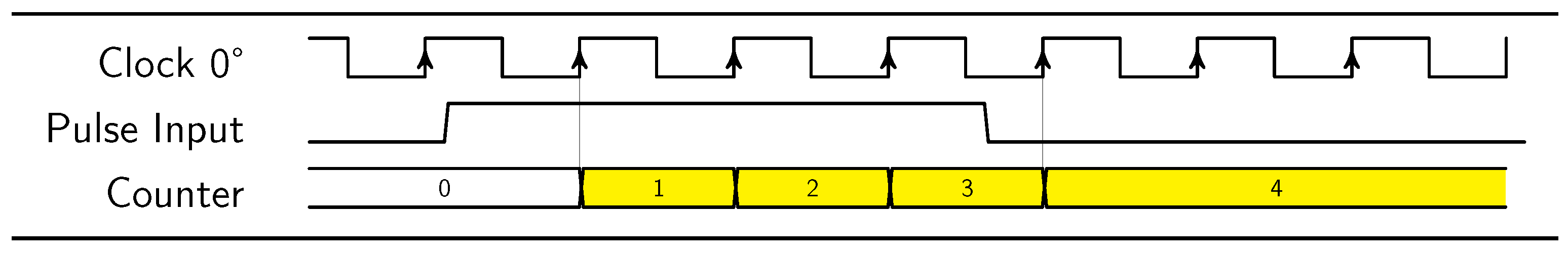
Figure 2.
Basic TDL architecture. The delay line goes through a line of FFs which are clocked with the same clock.
Figure 2.
Basic TDL architecture. The delay line goes through a line of FFs which are clocked with the same clock.
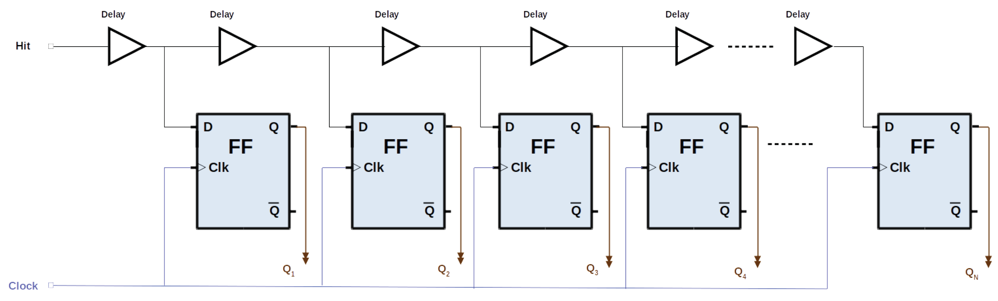
Figure 3.
Vernier Ring-Oscillator TDC basic scheme. The resolution is determined by the frequency difference between the two oscillators.
Figure 3.
Vernier Ring-Oscillator TDC basic scheme. The resolution is determined by the frequency difference between the two oscillators.
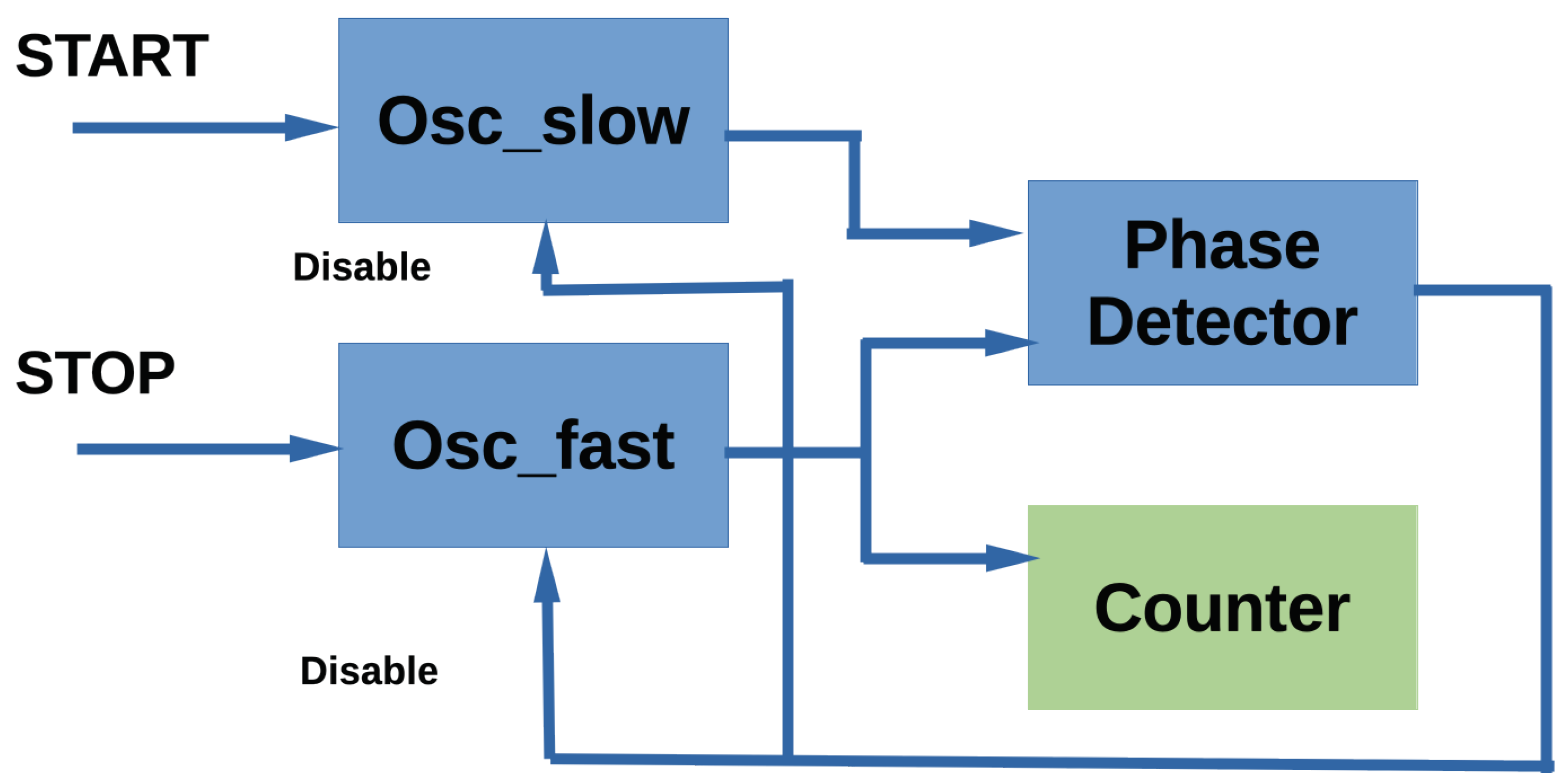
Figure 4.
Oversampling scheme, the basis of the MPSC-TDC. The resolution is increased by the number of phases.
Figure 4.
Oversampling scheme, the basis of the MPSC-TDC. The resolution is increased by the number of phases.
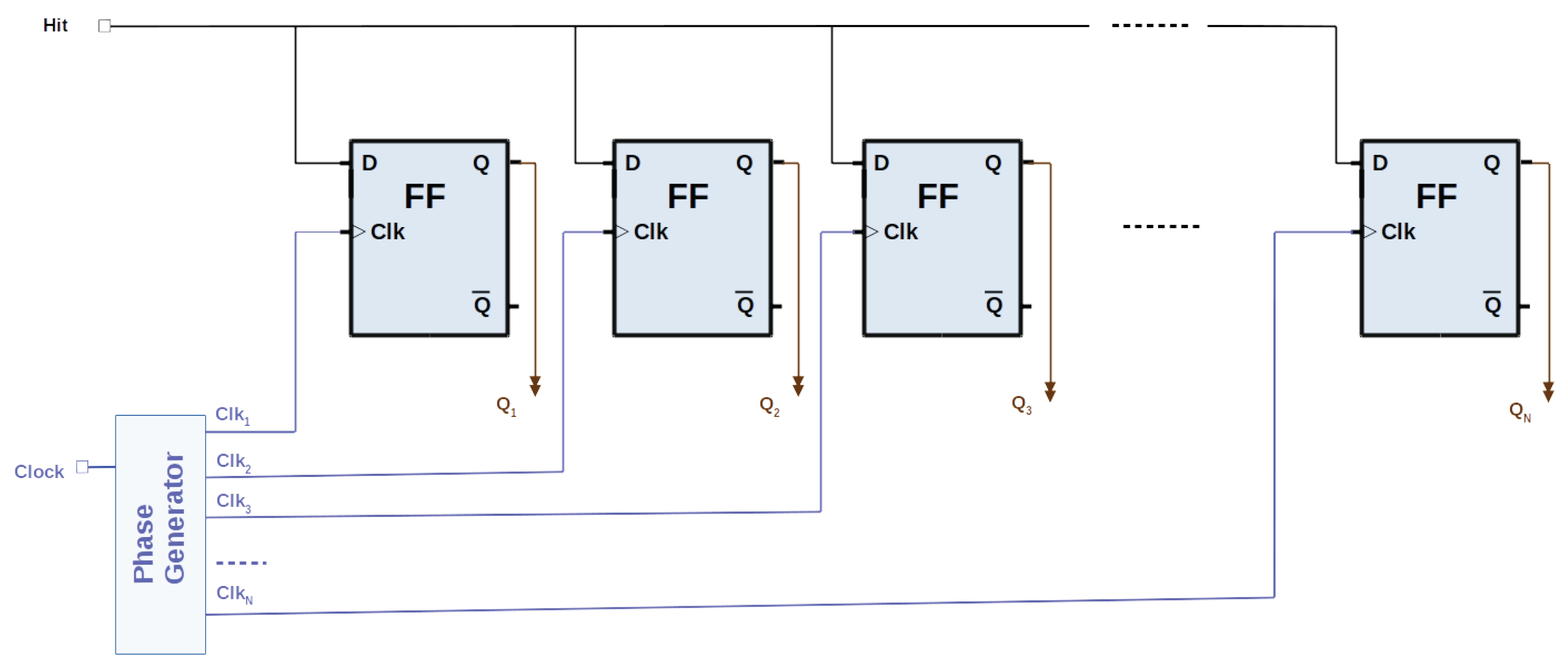
Figure 5.
Oversampling timeline. In this case, the basic counter resolution is expanded by four by using the rising and falling edges of two clock signals shifted 180°.
Figure 5.
Oversampling timeline. In this case, the basic counter resolution is expanded by four by using the rising and falling edges of two clock signals shifted 180°.
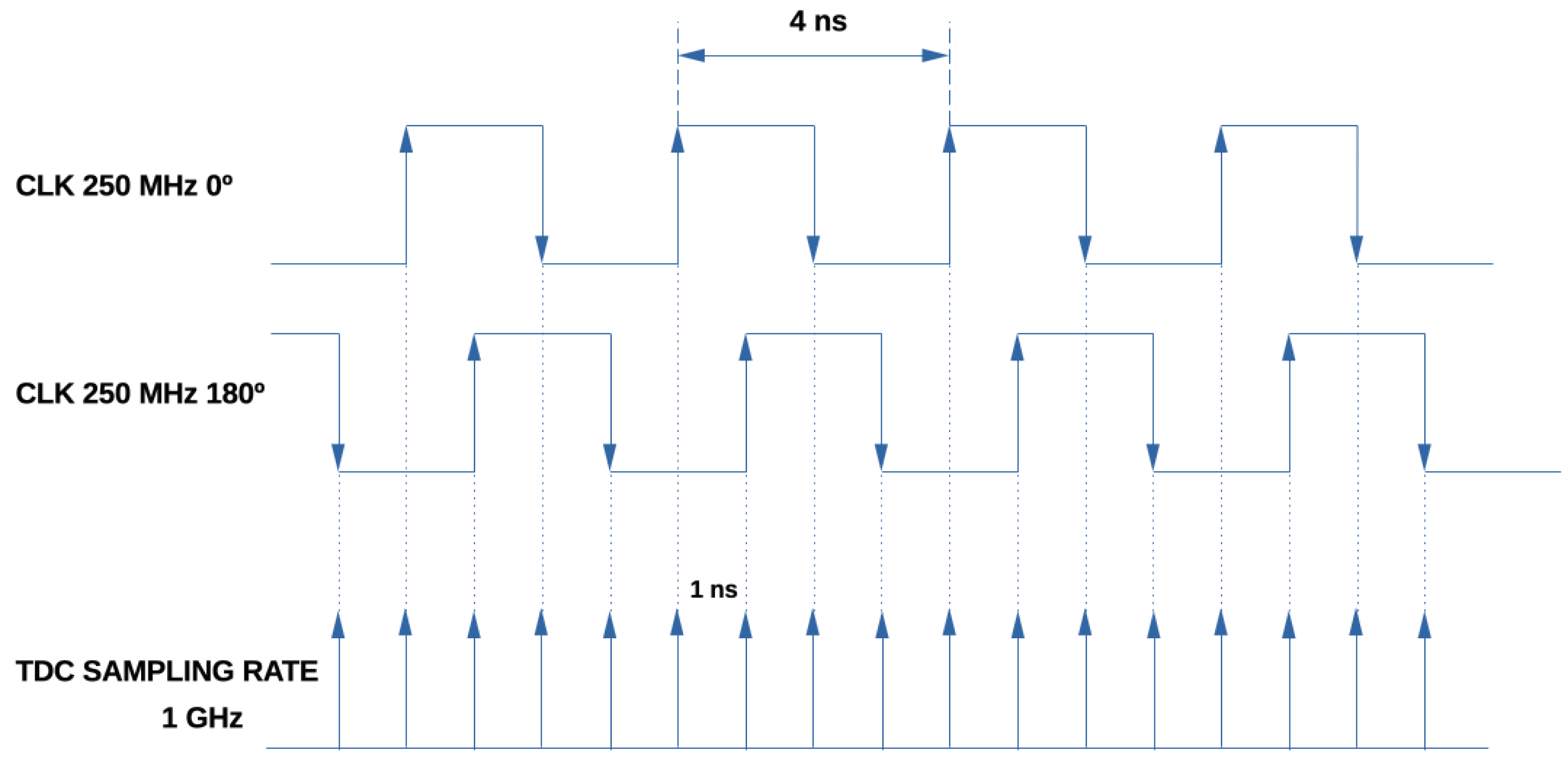
Table 2.
Low-resource TDC architectures: Advantages and drawbacks.
| Type | Advantages | Drawbacks |
|---|---|---|
| TDL | High-resolution | Calibration |
| PVT | ||
| Resource consumption | ||
| TDL:IODELAY | Resource efficient | Moderate resolution |
| PVT compensated | Limited number | |
| Delay granularity | ||
| VRO | High resolution | Resource consumption |
| slightly linear | ||
| high dead-time | ||
| GCO | Resource efficient | Calibration |
| PVT | ||
| MPSC | Resource efficient | Moderate resolution |
| Highly linear | ||
| MPSC:SerDes | Resource efficient | Moderate resolution |
| Highly linear | Limited number |
Disclaimer/Publisher’s Note: The statements, opinions and data contained in all publications are solely those of the individual author(s) and contributor(s) and not of MDPI and/or the editor(s). MDPI and/or the editor(s) disclaim responsibility for any injury to people or property resulting from any ideas, methods, instructions or products referred to in the content. |
© 2024 by the authors. Licensee MDPI, Basel, Switzerland. This article is an open access article distributed under the terms and conditions of the Creative Commons Attribution (CC BY) license (http://creativecommons.org/licenses/by/4.0/).
Copyright: This open access article is published under a Creative Commons CC BY 4.0 license, which permit the free download, distribution, and reuse, provided that the author and preprint are cited in any reuse.


