
Submitted:
19 February 2024
Posted:
20 February 2024
You are already at the latest version
Abstract
In this paper, a low-power Injection-Locked Clock and Data Recovery (ILCDR) using 28nm FDSOI technology is presented. The back-gate auto-biasing of UTBB-FDSOI transistors allows us to create a QRO (Quadrature Ring Oscillator) reducing both size and power consumption. By injecting a digital signal into this circuit, we realize an Injection-Locked Oscillator (ILO) with low jitter. Thanks to the good performance of this oscillator, we propose a low power ILCDR with fast locking time and low jitter for burst-mode applications. The main novelty consists in the implementation of a complementary QRO based on back-gate control using FDSOI technology to realize a simple and efficient ILCDR circuit. With a Pseudo-Random Binary Sequence (PRBS7) at 868Mbps, the recovered clock jitter is 26.7ps (2.3%UIp-p) and the recovered data jitter is 11.9ps (1%UIp-p). With a 0.6V power supply, the power consumption is 318μW. The estimated Chip area is around 6600μm².
Keywords:
Clock and Data Recovery (CDR)
; Quadrature Ring Oscillator (QRO)
; Injection-Locked Oscillator (ILO)
; Injection-Locked Clock and Data Recovery (ILCDR)
; burst-mode
; FDSOI technology
1. Introduction
Generally, synchronous data transmission systems send only the data signal to reduce the bandwidth and power consumption. The receiver has to implement a CDR circuit to perform both the extraction of the transmitted data sequence from the noisy received signal and the recovery of the associated clock timing information [1]. The data must be retimed to remove the jitter accumulated during transmission. The generated clock must have a frequency equal to the data rate and a low jitter because it is the main contributor to the retimed data jitter. To have an optimum sampling of the bits, the rising edges of the restored clock must coincide with the midpoint of each bit. In this case, the sampling occurs farthest from the previous and following data transitions, providing a maximum margin for jitter [2].
Indeed, 28nm FDSOI technology allows us to create a complementary inverter by using the back-gate of the transistor to symmetrize its outputs [3]. Complementary inverters allow us to implement back-gate auto-biasing feedback and to realize a QRO with an even number of inverters. By injecting a signal into this circuit, we create an ILO with low jitter [4]. Thanks to the good performance of this oscillator, we can propose a low-cost and low-power ILCDR with an improved jitter and a fast-locking time for burst-mode applications.
This paper is organized as follows: Section 2 introduces and compares the various types of open-loop CDR. Section 3 presents the circuit implementation of the injection complementary QRO based on the UTBB-FDSOI technology. The proposed ILCDR architecture and the simulation results are described in Section 4, followed by a conclusion of this work in Section 5.
2. CDR Architectures
CDR can be classified into two major categories. The first structures are using feedback phase tracking like Phase Locked Loop (PLL) or Delay Locked Loop (DLL). These closed-loop architectures are the most used essentially for their low jitter [1,2,5,6]. The second ones are open loop structures with low power, fast locking time, simple and low-cost design [7].
Open-loop CDR structures aim at local area network, passive optical networks and Serializer/Deserializer applications in which jitter accumulation is not a major problem but need a burst-mode operation to extract a synchronous clock and recover the received data quickly for each asynchronous packet [1,7,8,9]. An open-loop CDR is usually based on a gated oscillator, a high-Q bandpass filter, or an ILO circuit [7] as shown in Figure 1.
Driven by the recovered clock, the D Flip-Flop (DFF) retimes the incoming data. The variable delay buffer provides an adjustable delay of the input data to align it with the clock edge (the best time is the midpoint of each bit). It can be controlled externally to correct the Process, Voltage, and Temperature (PVT) variations. The edge detector is generally an XOR gate that will generate pulses at the input data bit frequency that commands the oscillator.
The high-Q filter-based CDR, such as an LC filter, directly samples the clock but its integration on a chip is difficult and there is no input jitter rejection [1,7]. The gated oscillator circuit aligns this phase by every input data transition, so it also has no input jitter rejection and a strong sensitivity to PVT variations [1].
We propose the implementation of an ILCDR to achieve a rapid acquisition time and robust jitter tolerance. Notably, this type of CDR exhibits an input-jitter-filtering nature, distinguishing it from CDRs relying on high-Q filter or gated oscillator [7,10]. Additionally, injecting the output of the edge detector into the ILO forces it to lock onto this frequency. This allows for some process variation in the oscillator design, thereby enhancing PVT variations tolerance. Certainly, injecting a periodic signal into an oscillator leads to pulling or locking phenomena [11]. Injection locking occurs when an oscillation source is shifted by an interference signal with a frequency very close to its own. In this case, the output frequency will be locked to the frequency of the interference signal instead of its own free-running frequency [4]. The principle of a simple injection structure is shown in Figure 2.
A three-stage ring oscillator oscillates at the frequency f0. The introduction of a phase shift ϕ0 in this loop modifies the oscillation frequency because the system phase deviates by a value equal to ϕ0. Figure 2b shows the change in the oscillation frequency from f0 to f1 induced by the effect of ϕ0. Assuming that ϕ0 is generated by an injection voltage V𝑖𝑛𝑗, the system then oscillates at the injection frequency f𝑖𝑛𝑗 [4].
The ILCDR structure may include a closed-loop, typically designed with a PLL, to conduct on the input data a frequency tracking and adjust the free-running frequency of the ILO, as illustrated in Figure 3.
In case of a long sequence of 0 or 1, the input frequency tracking system improves the BER of the ILCDR by reducing the difference between the free-running frequency and the input data frequency of the ILO [7]. Adding a PLL increases the cost, the complexity, the power consumption, and the die area of the CDR. In this study, our proposition aims to enhance the jitter of the standard architecture of the open-loop ILCDR without utilizing a PLL, thus maintaining a low-cost and low-power design.
3. Injection complementary QRO
3.1. RO Design
To perform a quadratic demodulation, it is necessary to have at least two 90° phase shifted signals. A VCO enables this operation to be carried out [12]. LC tanks are the most popular circuits to realize a VCO. On the contrary, RO is known to exhibit high phase noise, but this design will address aggressively the size and power consumption reduction. We have proposed a new inverter topology to realize a VCO using FDSOI technology [13].
The access to UTBB (Ultra-Thin Body & Box) transistor Back-Gates offers an extended control of the threshold voltages of the transistors (cf. Figure 4 and Figure 5) [14], opening new opportunities to exciting performances. We have proposed a new complementary structure based on a pair of Back-gate cross-coupled inverters offering a fully symmetrical operation of complementary signals, as shown in Figure 6 [3].
The main idea is as follows: frequently, the NMOS transistor, the faster one, is going to accelerate the conduction of the slower PMOS transistor, and reciprocally. So, connecting the output of each inverter to the back-gate of the other, the faster stage will accelerate the slower one, realizing a symmetrization of the two stages. The complementary outputs are crossing at VDD divided by 2. Monte Carlo (MC) simulations exhibit a mean value of VDD /2 = 500mV, and the standard deviation is about σ = 2.7mV [13].
This new complementary inverter will offer two other advantages very important for ring oscillator realization. The first one concerns the duty cycle, which has to be close to 50% and low jitter [3]. Secondly, this topology enables an oscillator with an even number of inverters (cf. Figure 7). This latter feature makes it easy to perform a QRO: four identical outputs with the same amplitude and same frequency but with different phases (0°, 90°, 180°, and 270°).
Figure 7.
QRO with four inverters (back-gates cross-coupled in blue).
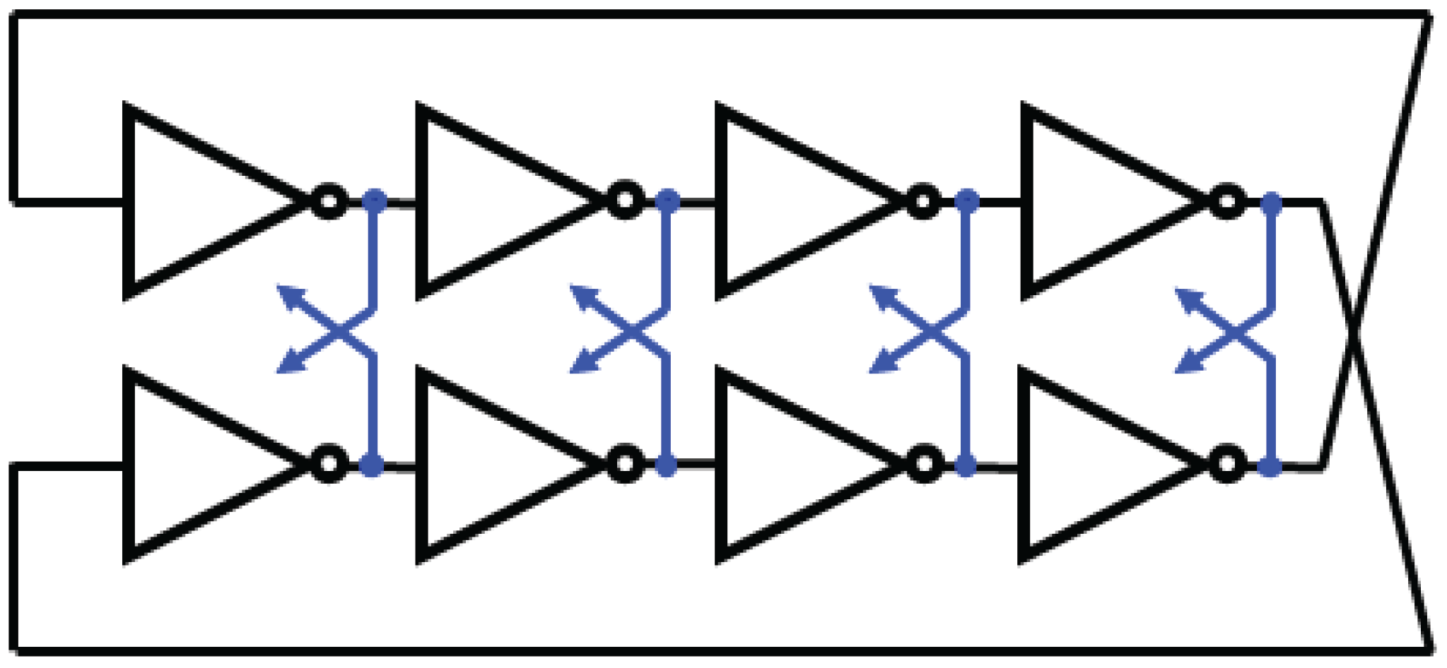
Figure 8.
Transient simulation results of the QRO [13].
Figure 8.
Transient simulation results of the QRO [13].
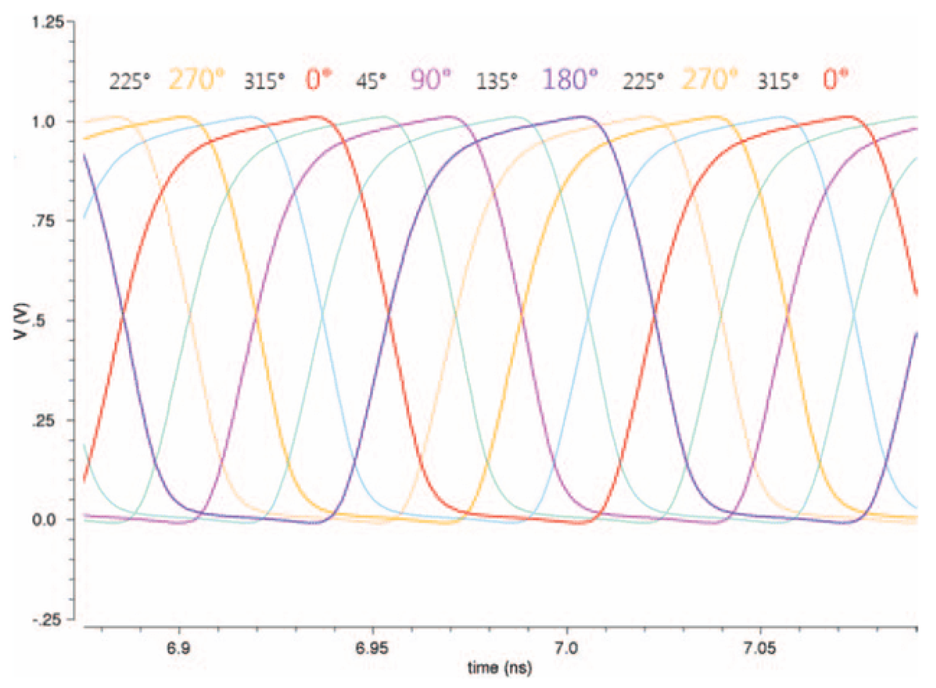
The transient result is shown in Figure 8, where the complementary outputs are crossed at VDD divided by 2. The 8 single-ended outputs are plotted which produces a clock equally spaced by 45°. In CDR, the 8-phase output provides the ability to create a variable delay.
3.2. Injection complementary QRO
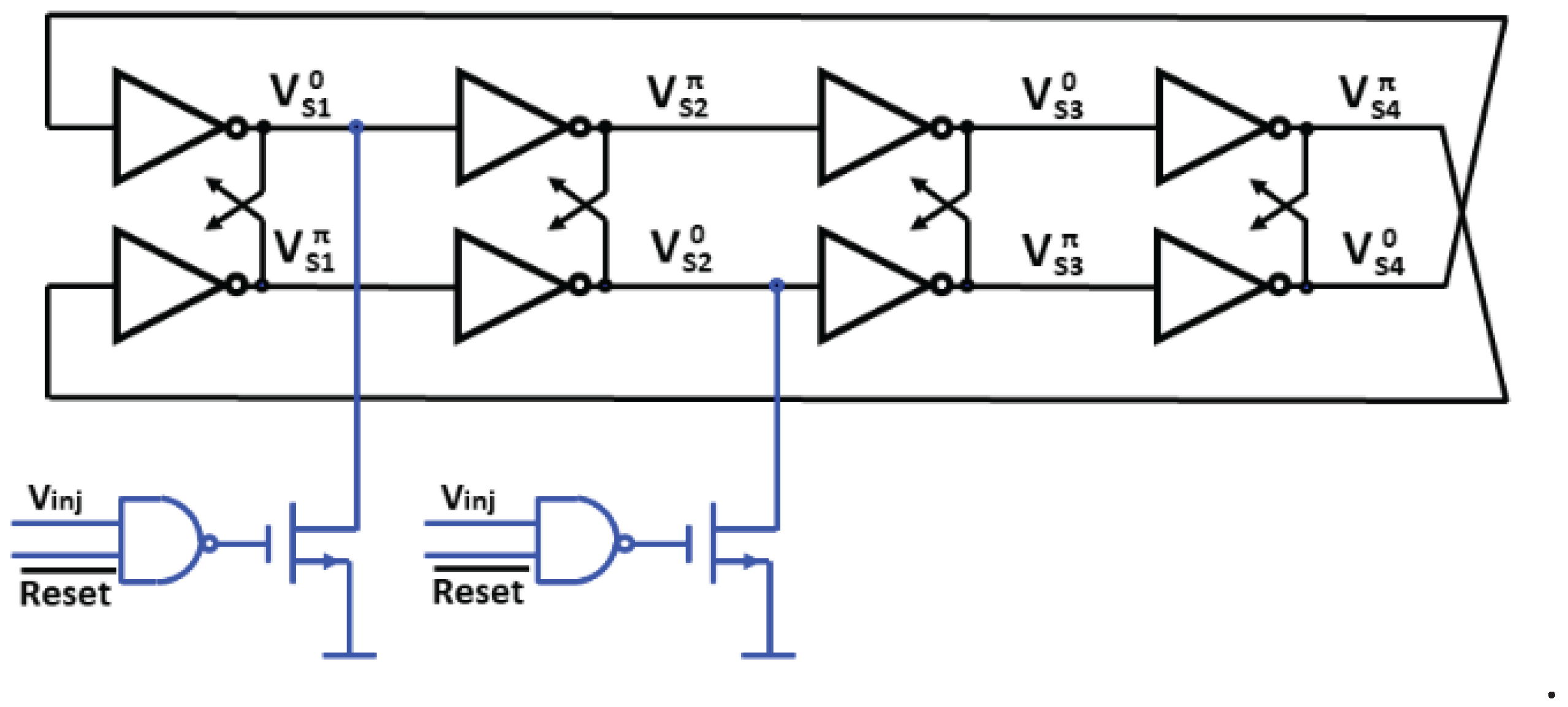
Figure 9 shows the schematic of the proposed design. The QRO may not oscillate automatically, so it needs a startup design. The complementary signal output for a complementary inverter is a necessary condition for the oscillator to start. The use of NMOS transistors as switch can only pull the voltage down to 0, and the complementary signal can be obtained from the output of the next stage inverter, so a two-stage complementary inverter should be considered to study the start of the oscillator [15].
To ensure normal oscillation of the QRO and obtain a complementary signal pair, the initialization configuration should involve initializing both outputs: one from the first stage and the other output of the second stage (Reset). Simultaneously, the injection signal Vinj is also transmitted through the two NMOS transistors to generate the complementary signals.
To make the Reset signal and the injected signal work together and not interfere with each other, it is necessary to use these two signals as the two input signals of a NAND gate. In practice so as not to unbalance the different outputs of the QRO, the same capacitance values C of the Reset transistors (T1 and T2) will be added to all the other outputs.
Figure 9.
Single injection complementary QRO (injection and reset in blue).
According to the principle of injection locking, this structure can expand the range of oscillation frequency. The circuit starts to oscillate when VDD is 0.4V, and as VDD increases, the locking range becomes larger.
When the oscillation frequency is 868MHz, the injection locking range can be expanded from 690MHz to 1GHz, which is 36% of 868MHz, as shown in Figure 10.
Figure 11 compares the relationship between oscillation frequency and phase noise with or without injection signal. Due to thermal noise and flicker noise, the phase error of a free-running QRO will increase randomly compared to an ideal QRO. The injection pulse forces the edge of the output signal to move back to the correct position every injection period, so the phase error no longer accumulates, and the phase noise can be reduced. In contrast, the phase noise measured at 1MHz is -117dBc/Hz, which is 34dB less than the phase noise of no injection signal.
4. Proposed ILCDR
4.1. Timing analysis of the proposed ILCDR
Figure 12 depicts a simplified block diagram of the injection CDR. The input signal is a PRBS7 at 868Mbps. After the pulse generator, a pseudo-random pulse signal is obtained at the rate multiplied by 2, which is 1.736Gbps. After injecting the pulse signal into the complementary RO, it outputs a periodic signal with a frequency of 868MHz, which is the recovered clock signal. The recovered data signal is the output signal with a rate of 868 Mbps after sampling.
Equation 1 indicates the behavior of the injection current pulse:
where γ denotes the pulse width and T denotes the period of the injected pulse [16]. Experimental results on the 8 quadrature-phase output signals of the complementary RO show that the maximum value of γ needs to be less than 0.5T to achieve an acceptable jitter. Indeed, injection intensity is related to the duty cycle of the injection signal, which affects the injection performance. The best pulse signal width obtained to minimize the jitter of the ILCDR system is equal to a quarter bit period (Tb/4) as shown in Figure 13.
4.2. Architecture
Figure 14 illustrates the architecture of the proposed full-rate ILCDR, which includes a pulse signal generation block consisting of a DFF and an XNOR gate, an injection block, and a complementary RO block. The incoming data, NRZ code, whose power spectral density is zero at the frequency component of the clock or its multiples, the clock signal cannot be extracted. By passing the NRZ data through a DFF and an exclusive-OR gate, RZ data can be obtained from which the clock frequency components may be extracted [17]. Injecting the pulse signal Minj into a complementary ring oscillator, it outputs eight periodic signals with the same rate and different phases. One of these 8-phases signals is selected as the clock signal which contains a variable phase, so a variable delay consisting of several inverters is no longer required, which could simplify the circuit structure and thus reduce the power consumption and the chip size of the ILCDR. One of the 8 phases is manually selected in the simulation stage and is sent to the DFF. A binary selector and an 8-to-1 MUX will be used to select the phase for the manufacturing stage. The principle of manual selection is to obtain smaller jitter. Indeed, the output signal makes the injection pulse width matches Tb/4 minimizing the jitter of CDR circuit. The input data is XNORed with the output signal of the DFF to obtain a pulse signal with 2 times the bit rate. The recovery data Dout is obtained after the decision circuit DFF clocked by the recovered clock CKOUT.
In general, the QRO takes advantage of the back-gate control structure that reduces the error in each transition. Random jitter (thermal noise, flicker noise, etc.) can be corrected periodically using injection techniques. Furthermore, a DFF was used to implement the functions of pulse signal generation and recovery data sampling simultaneously.
4.3. Schematic simulation results
We used the 28nm UTBB-FDSOI transistor model of STMicroelectronics. The proposed ILCDR achieves a wide operation range of 868Mbps in a Cadence Analog Design Environment with a 0.5V supply voltage. The dimensions of the RO transistors are 4.1µm/30nm for the PMOS and 2µm/60nm for the NMOS.
Figure 15 illustrates the results of transient simulations performed on the complementary ILCDR, where Din is the input data, ROout is the output of the injected complementary ring oscillator, CK is the recovered clock signal and Dout is the recovered data. Simultaneously, Figure 16 shows the variation curve of frequency during the locking process. The figure illustrates that when the input data is a PRBS7 random data with an 868Mbps data rate, the locking time of the ILCDR is about 5ns, and the clock frequency stabilizes around 868MHz after locking.
Based on over 10,000 cycles of transient simulations, Figure 17 shows the jitter of the recovered clock and recovered data for the PRBS7 input data. The jitter is 7.4ps (0.6%UI) of the clock and 2.3ps (0.2%UI) of the PRBS7 data. The locking range is 860-1100Mbps without errors of the input PRBS7, which is 28% of 868 Mbps.
Figure 18 presents the phase noise when a periodic injection signal is introduced. The phase noise for the injection circuit is -122dBc/Hz@1MHz.
It is obtained from transient simulation that when the input data is a random code of PRBS7 at 868Mbps, the power consumption is 235μW when the CDR circuit is locked. The percentage of power consumption of each part of the circuit is shown in Figure 19, where the RO consumes 49μW and the other modules consume 186μW. The power efficiency of CDR is:
In our CDR circuit, the frequency of the RO is directly controlled by VDD. Therefore, our focus will be on process and temperature variations. Table 1 shows the output frequency of the CDR for the 868Mbps PRBS7 input data in different cases, including the fastest case (FF corner with 125°C) and the slowest case (SS with corner -40°C) [18].
Based on the results in Table 1, it can be observed that temperature has a more significant impact on the structure for an input rate of 868Mbps, leading to harmonic injection in both the fastest and slowest cases. In the fastest case, the output frequency is close to 2*868MHz, resulting in 1.736GHz. Conversely, in the slowest case, the output frequency is close to 868MHz/2, resulting in 434MHz.
A Monte Carlo, incorporating random statistical variation, was conducted on the ILCDR to analyze the resulting clock frequency, involving 500 data points. The histogram plot in Figure 20 illustrates the approximate probability distribution.
Despite the mean of the output clock frequency being 865MHz (i.e 864.8MHz), a significant concentration of data points is observed near 868MHz. The standard deviation is calculated to be 9.6MHz. The MC simulation reveals that the variability attributed to the manufacturing process on the oscillation frequency remains low, approximately 3σ/Mean=27/868=3.1% maximum relative deviation.
4.4. Layout design and post-layout simulation
Figure 21 illustrates the structural arrangement of the complementary inverter layout topology. In this configuration, a symmetrical layout of four transistors and their corresponding ports is displayed, taking advantage of the balanced arrangement between the various circuit elements. This symmetry serves a dual purpose: firstly, it helps to simplify the complex circuit layout and secondly, it has a key role in enhancing the overall stability of the system.
Figure 22 illustrates the configuration of the complementary inverter, detailing the precise placement and interconnections of the transistors and ports, with a layout area of approximately 8×8μm².
Figure 23 graphically illustrates the layout configuration of a complementary RO. In this case, the fundamental objective is to systematically organize the four complementary inverters into a symmetrical layout. The symmetrical arrangement is designed to minimize these parasitic effects, thereby enhancing the signal integrity and overall performance stability of the complementary ring oscillator. Figure 24 provides a comprehensive view of the layout design of the complementary RO, including the start-up circuit.
First, the schematic and layout of the complementary inverter were simulated for comparative analysis. The transient simulation results are shown in Figure 25. The results of the schematic simulation and the post-layout simulation are consistent to a large extent, with the main difference being that the rise time (tr) and the fall time (tf) of the post-layout simulation are both slightly extended.
Based on this framework, we performed a similar comparative analysis for the simulation of a complementary RO. In the schematic simulation, the oscillator operates at a frequency of 868MHz with a supply voltage of 0.5V. However, in post-layout simulations, the oscillation frequency decreases to 285MHz with a supply voltage of 0.5V. This reduction can be attributed to resistance effects and parasitic capacitance.
Figure 25.
Transient simulation results for complementary inverter.
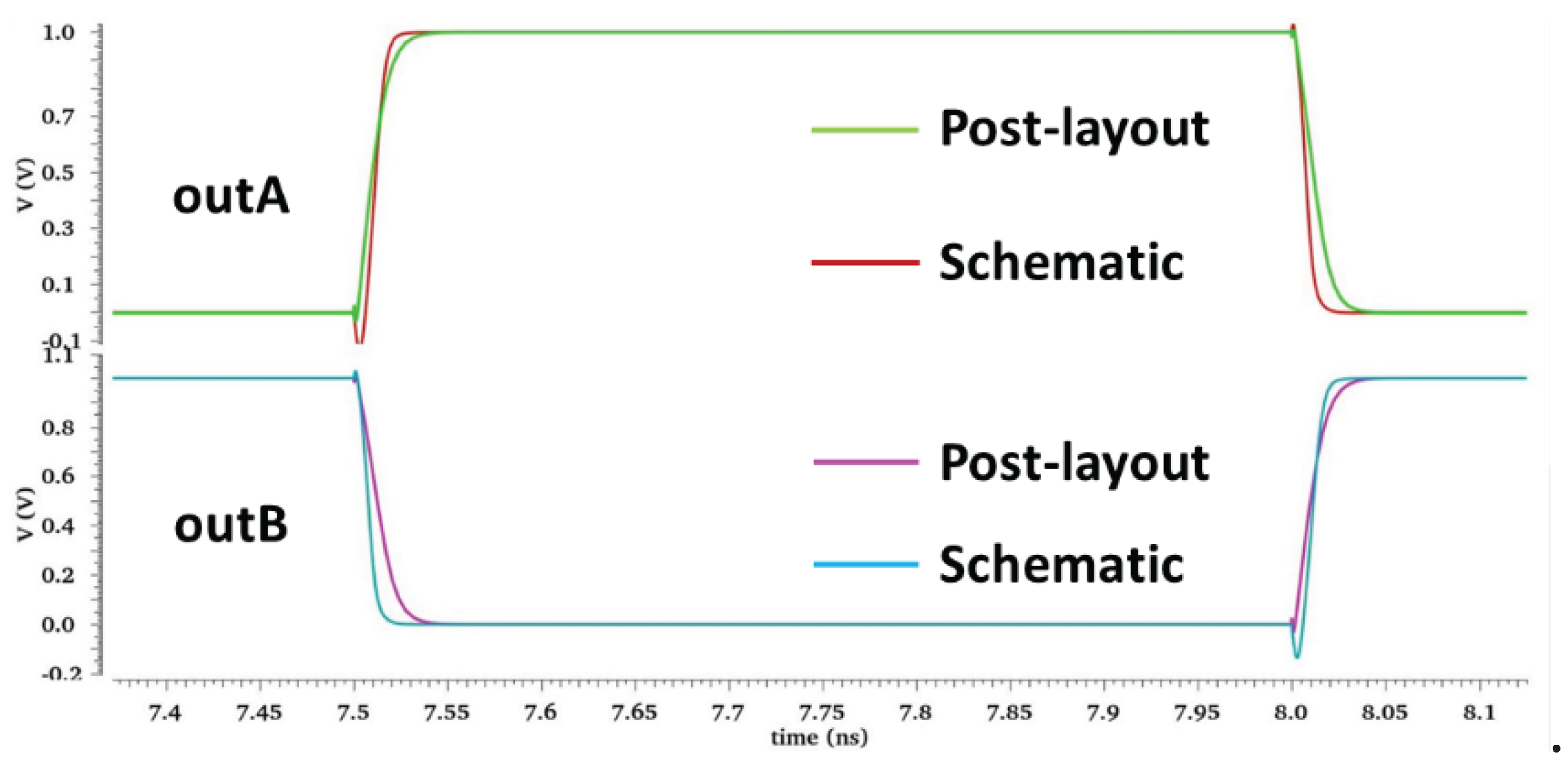
Figure 26 depicts the transient simulation results.
To compensate for resistance effects and parasitic capacitance in the layout, we have adjusted the VDD from 0.5V to a higher level of 0.63V. The aim was to achieve 868MHz ILCDR operational functionality. This has been shown to help reduce the effects of parasitic components, thus contributing to the expected performance of the ILCDR. The adjusted ILCDR has a locking time of approximately 5ns and the clock frequency is stabilized around the 868MHz target frequency.
After confirming the proper functionality of the CDR circuit, we turned our focus to assessing the jitter performance of both the clock and the output data using eye diagram analysis. Figure 27 presents these findings, indicating a clock jitter of around 26.7ps (2.3% UI) and a recovered data jitter of approximately 11.9ps (1% UI). Moreover, when exposed to a periodic input signal, this CDR demonstrates a phase noise of -118dBc/Hz@1MHz. The ILCDR consumes 318μW, and the power efficiency is 0.318/0.868 = 0.37pJ/bit.
Table 2 offers a performance comparison between the schematic and post-layout simulations. The post-layout results reveal an increase in phase noise and peak-to-peak jitter compared to the schematic outcomes. This difference is attributed to the impact of parasitic resistance and parasitic capacitance associated with the metal interconnects on the RO's performance. Furthermore, the elevation of VDD to achieve the target frequency of 868MHz leads to higher power consumption in post-layout simulation.

Table 2.
Comparison between schematic and post layout of the ILCDR at 868MHz.
| VDD (V) | CK jitter | PN (dBc/Hz@1MHz) | Power consumption (μW) | |
| Schematic | 0.5 | 0.6%UI | -122 | 235 |
| Post-layout | 0.63 | 2.3%UI | -118 | 318 |
Table 3 enumerates the schematic and post-layout simulation outcomes for the complementary ILCDR under various processes and temperatures. Notably, the post-layout simulation results exhibit relatively greater stability during the process and temperature variations compared to the schematic because the VDD is increased to 0.63V in the post-layout (0,5V in schematic). Indeed, in our CDR circuit, the frequency of RO is directly controlled by VDD. To improve frequency stability with respect to temperature, we are considering implementing the solution proposed by [19], which is simple and low power.
5. Conclusions and state of the art comparisons
A performance comparison between some recently published CDRs and our work is presented in Table 4.
Thanks to FDSOI technology, we have proposed to implement a novel cross-coupled back-gate technique to improve analog and mixed signal cells and to decrease the surface of the integrated circuit. Thanks to this technique, we implemented a QRO based on complementary logic and inverters. This type of QRO is very efficient for low power and low frequency applications. Based on the back-gate structure, the proposed ILCDR significantly simplifies the design and, therefore, greatly reduces power consumption and surface. The ILCDR extracts an 868MHz clock signal for the same bit rate as random input data. Featuring back-gate and injection technology, it exhibits a desirable jitter performance.
Subsequently, we conduct a post-simulation analysis of the ILCDR. Despite the oscillation frequency reduced to one-third of the schematic level due to resistance effects and parasitic capacitance in the post simulation, we successfully achieve the expected frequency of the CDR by increasing the VDD. The peak-to-peak jitter is 26.7ps (2.3%UIp-p) and 11.9ps (2.3%UIp-p) for the recovered clock and data signal, respectively. The power consumption for the ILCDR is 318μW and the power efficiency of 0.37pJ/bit is relatively good. In the post layout simulations at 868MHz, the power consumption rises by 35%, and the phase noise increases by 4dB compared to the schematic simulation results. Despite this, the ILCDR maintains its attributes of low power, small surface area, and substantial energy efficiency. Our next step is to add a circuit [19] to improve the stability of the frequency as the function of temperature.
Author Contributions
Circuit idea, G.J. and Y.M.; circuit design, Y.M. and Y.C.; software, Y.M. and Y.C.; writing—original draft preparation, Y.M. and Y.C.; writing—review and editing, Y.M., Y.C., Y.L., and G.J. All authors have read and agreed to the published version of the manuscript.
Funding
This research received no external funding except for Ms. Mao's thesis grant (supported by the China Scholarship Council for 3 years of study at the Université Côte d’Azur under Grant No. 202008070128)
Data Availability Statement
All results and other data are available on request from the authors.
Conflicts of Interest
The authors declare no conflicts of interest.
References
- Hsieh, M; Sobelman, G. Architectures for multi-gigabit wire-linked clock and data recovery. IEEE Circuits and Systems Mag. 2008, 8, 45-57. [CrossRef]
- Razavi, B. Challenges in the design high-speed clock and data recovery circuits. IEEE Communications Mag., 2002, 40, 94-101. [CrossRef]
- Wei, Z.; Leduc, Y.; de Foucauld, E; Jacquemod, G. Novel Building Blocks for PLL Using Complementary Logic in 28nm UTBB-FDSOI Technology. In Proceedings of IEEE NewCAS, Strasbourg, France, 2017, pp. 121-124. [CrossRef]
- Mao, Y.; Charlon, Y.; Debieu, F.; Wei, Z.; Leduc, Y.; Jacquemod, G. Ultra low power injection-locked ring oscillator architecture using FDSOI technology. In Proceedings of the AVIC, Bordeaux, France, 2021. [Google Scholar]
- Wang, Y.; Zhang, L.; Han, W.; Li, X.; Lai, F.; Liu, X. A low-jitter PLL with new cross-coupled VCO delay cell for SerDes CDR in 55-nm CMOS technology. In Proceedings of IEEE ICSICT, 2016, pp. 1434-1436. [CrossRef]
- Liu, Y.; Wang, Y.; Jia, S.; Zhang, X. 180.5Mbps-8Gbps DLL-based clock and data recovery circuit with low jitter performance. In Proceedings of IEEE ISCAS, 2015, pp. 1394-1397. [CrossRef]
- Béraud-Sudreau, Q. et al., SiGe Clock and Data Recovery System Based on Injection-Locked Oscillator for 100 Gbit/s Serial Data Link. IEEE Journal of Solid-State Circuits 2014, 49, 1895-1904. [CrossRef]
- Yan, D. L.; Raja, M. K.; Ajjikuttira, A. B. A Gated-Oscillator based Burst-Mode Clock and Data Recovery (CDR) Circuit. In Proceedings of IEEE RFIT, Singapore, 2007, pp. 90-93. [CrossRef]
- Maruko, K.; et al. A 1.296-to-5.184Gb/s Transceiver with 2.4mW/(Gb/s) Burst-mode CDR using Dual-Edge Injection-Locked Oscillator. In Proceedings of IEEE ISSCC, San Francisco, CA, USA, 2010, pp. 364-365. [CrossRef]
- Han, P.S.; Choi, W.Y. 10Gbps injection-locked CDR with a simple bit transition detector in 0.18 μm CMOS technology. IEICE electronics express 2009, 6, 35–39. [Google Scholar] [CrossRef]
- Razavi, B. A study of injection locking and pulling in oscillators. IEEE J. Solid-State Circuits 2004, 39, 1415–1424. [Google Scholar] [CrossRef]
- Jacquemod, G.; Ben Abdeljelil, F.; Tatinian, W.; Lucchi, P.; Borgarino, M.; Carpineto, L. Comparison between RTW VCO and LC QVCO 12 GHz PLLs. Analog Integr Circ Sig Process, 2012, 73, 749–756. [Google Scholar] [CrossRef]
- Wei, Z.; Jacquemod, G.; Lorenzini, P.; Hameau, F.; de Foucauld, E.; Leduc, Y. Study and reduction of variability in 28nm Fully Depleted Silicon on Insulator technology. Journal of Low Power Electronics, 2016; 12, 64–73. [Google Scholar] [CrossRef]
- Clerc, S.; Di Gilio, T.; Cathelin, A. The Fourth Terminal: Benefits of Body-Biasing Techniques for FDSOI Circuits and Systems; Springer: Cham, 2020. [Google Scholar] [CrossRef]
- Wei, Z. Back-gate feedback for auto-calibration of analog and mixed cells in UTBB-FDSOI technology. Ph.D. dissertation, Université Côte d'Azur, 2019. English. NNT : 2019AZUR4033.tel-02493990v2. [Google Scholar]
- Borjkhani, H.; Sheikhaei, S.; Borjkhani, M. Low Power Current Starved Sub-Harmonic Injection Locked Ring Oscillator, In Proceedings of ICEE, Tehran, Iran, 2014, pp. 38-42. [CrossRef]
- Béraud-Sudreau, Q. Analysis and design of an 80 Gbit/sec clock and data recovery prototype. Ph.D. dissertation, Université Sciences et Technologies - Bordeaux I, 2013. English. NNT: 2013BOR14765.tel-00821890. [Google Scholar]
- Dasdan, A.; Hom, I.; Handling inverted temperature dependence in static timing analysis. ACM Trans. Des. Autom. Electron. Syst., 2006 11, pp. 306–324. [CrossRef]
- Samal, L.; Sahoo, S. R.; Samal, C. A Novel Temperature Invariant Ring Oscillator for Low Power Application, In Proceedings of IEEE IICPE, Jaipur, India, 2018, pp. 1-5. [CrossRef]
- Jin, J.; et al. A 4.0-10.0-Gb/s Referenceless CDR with Wide-Range, Jitter-Tolerant, and Harmonic-Lock-Free Frequency Acquisition Technique. In Proceedings of ESSCIRC, Dresden, Germany, 2018, pp. 146-149. [CrossRef]
- Choo, M. S.; Park, K.; Ko, H. G.; Cho, S. Y; Lee, K.; Jeong, D. K. A 10-Gb/s, 0.03-mm2, 1.28-pJ/bit Half-Rate Injection-Locked CDR With Path Mismatch Tracking Loop in a 28-nm CMOS Technology. IEEE Journal of Solid-State Circuits, 2019 54, pp. 2812-2822. [CrossRef]
- Wang, M.; Chen, Y.; Yuan, J. A low jitter 50Gb/s PAM4 CDR of Receiver in 40nm CMOS Technology. In Proceedings of WCSP, Nanjing, China, 2020, pp. 349-352. [CrossRef]
- Lee, H. W.; Ko, K. M; Kang, J. K. An 8 - 26 Gb/s Single Loop Reference-less CDR with Unrestricted Frequency Acquisition. In Proceedings of ISOCC, Jeju Island, Korea, Republic of, 2021, pp. 45-46. [CrossRef]
- Vert, D.; Pignol, M.; Lebre, V.; Moutaye, E.; Malou, F.; Begueret, J.B. A 3.2 GHz Injection-Locked Ring Oscillator-Based Phase-Locked-Loop for Clock Recovery. Electronics, 2022 11, 3590. [CrossRef]
Figure 1.
Standard architecture of an open-loop CDR [7].
Figure 1.
Standard architecture of an open-loop CDR [7].
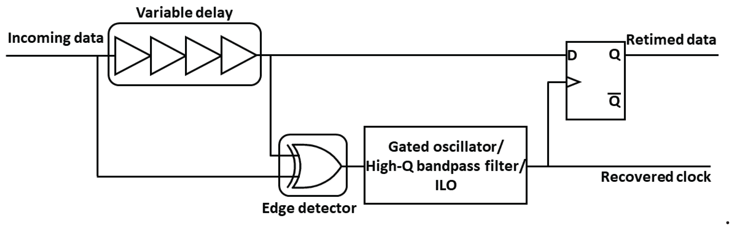
Figure 2.
Injection modelling in a Ring Oscillator (RO) [4] : (a) RO with injection; (b) Oscillation frequency shift.
Figure 2.
Injection modelling in a Ring Oscillator (RO) [4] : (a) RO with injection; (b) Oscillation frequency shift.
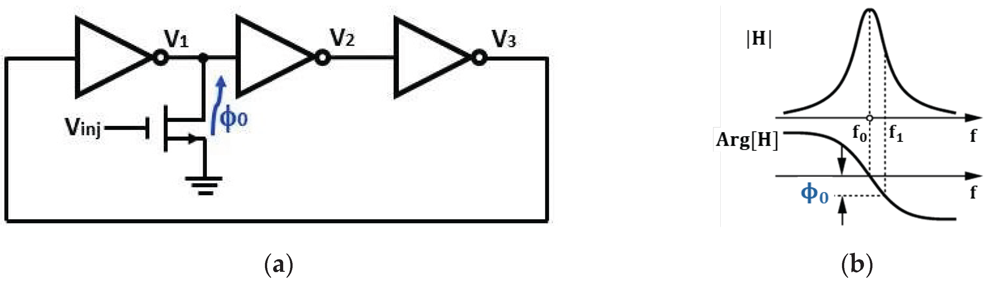
Figure 3.
ILCDR structure with an input frequency tracking system [7].
Figure 3.
ILCDR structure with an input frequency tracking system [7].
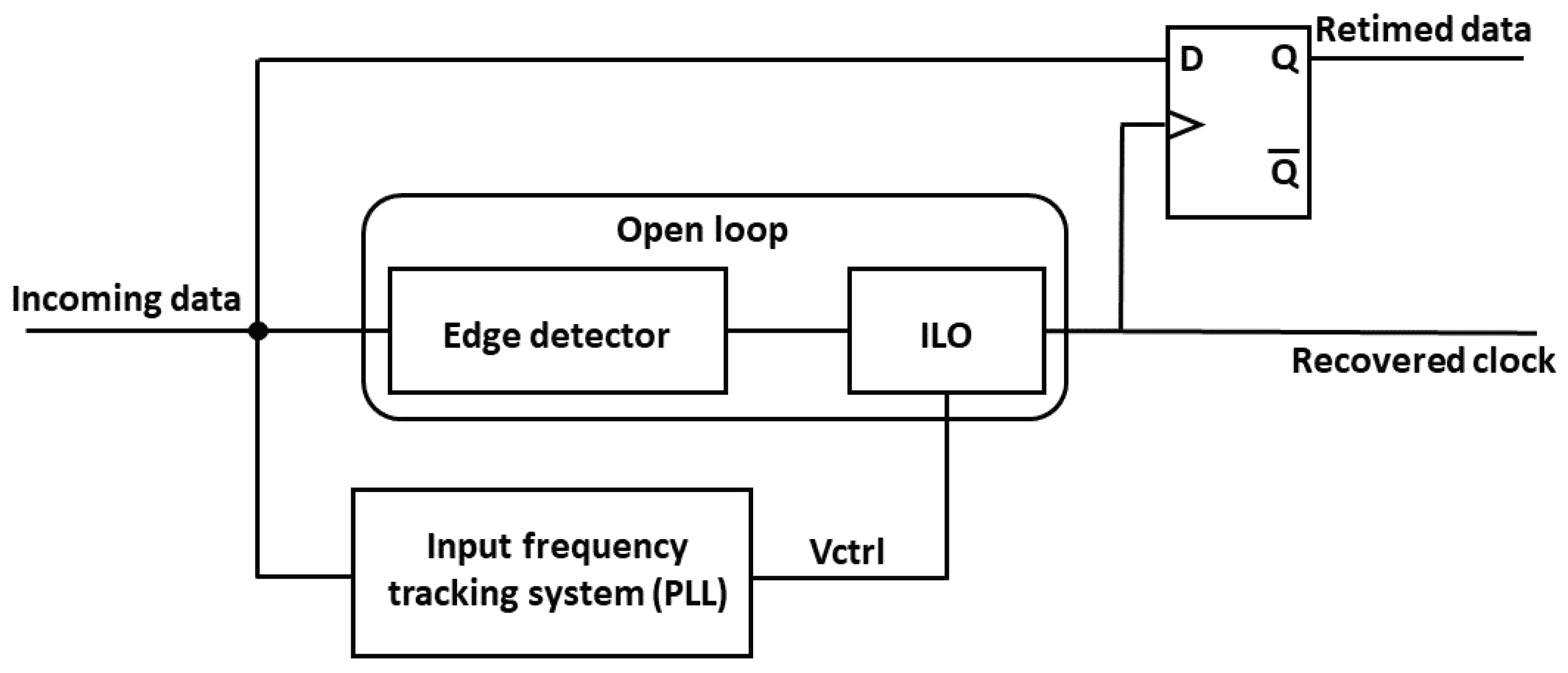
Figure 4.
Back gate biasing.
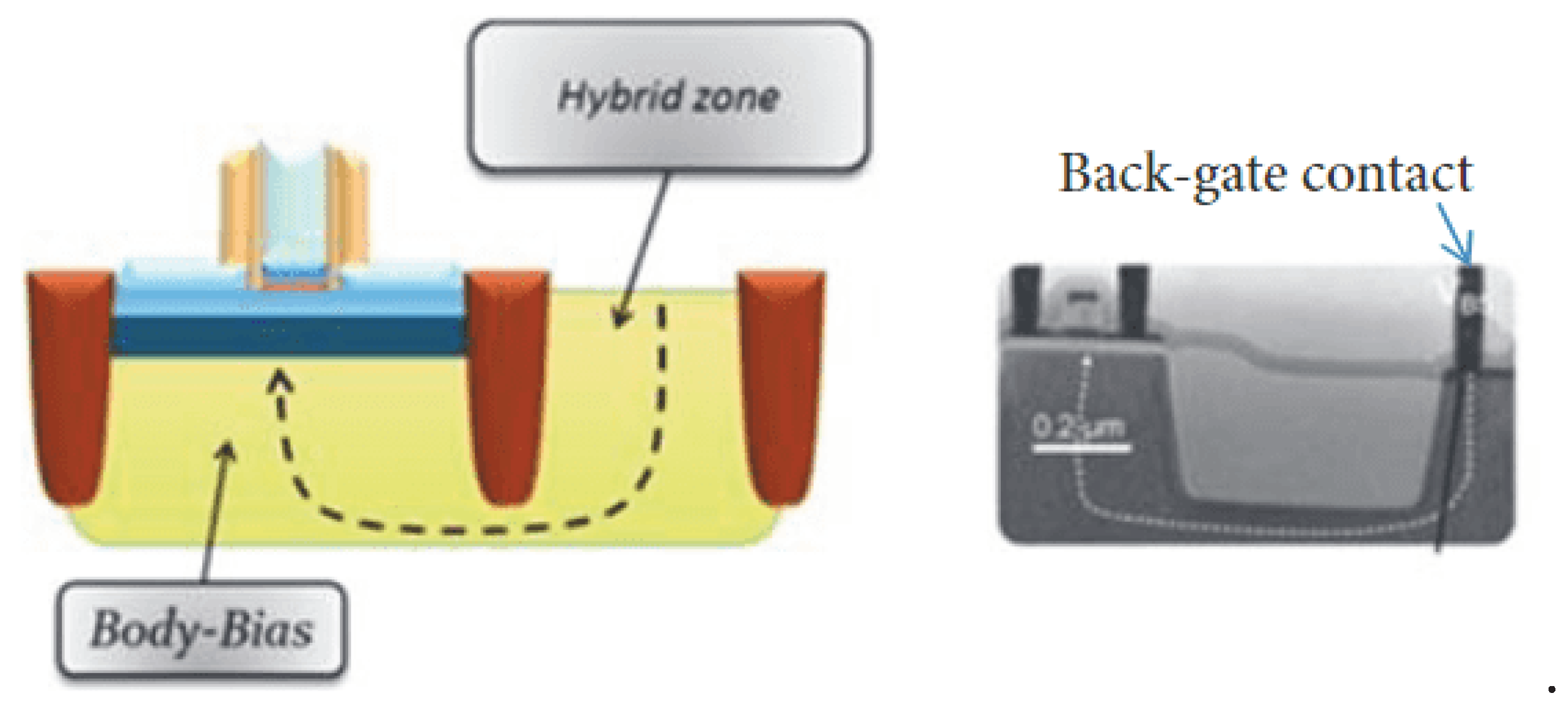
Figure 5.
Body-biasing effect for similar size transistors in 28nm FDSOI (blue curve) and bulk (red curve) from STMicroelectronics [14].
Figure 5.
Body-biasing effect for similar size transistors in 28nm FDSOI (blue curve) and bulk (red curve) from STMicroelectronics [14].
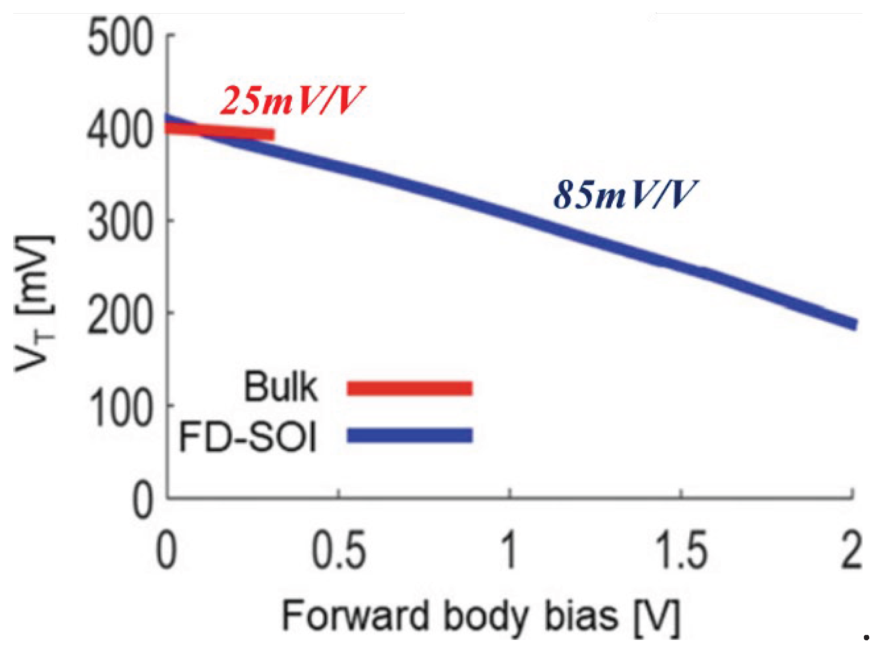
Figure 6.
Complementary inverter based on a pair of back-gate cross-coupled (blue and red wires) [3].
Figure 6.
Complementary inverter based on a pair of back-gate cross-coupled (blue and red wires) [3].
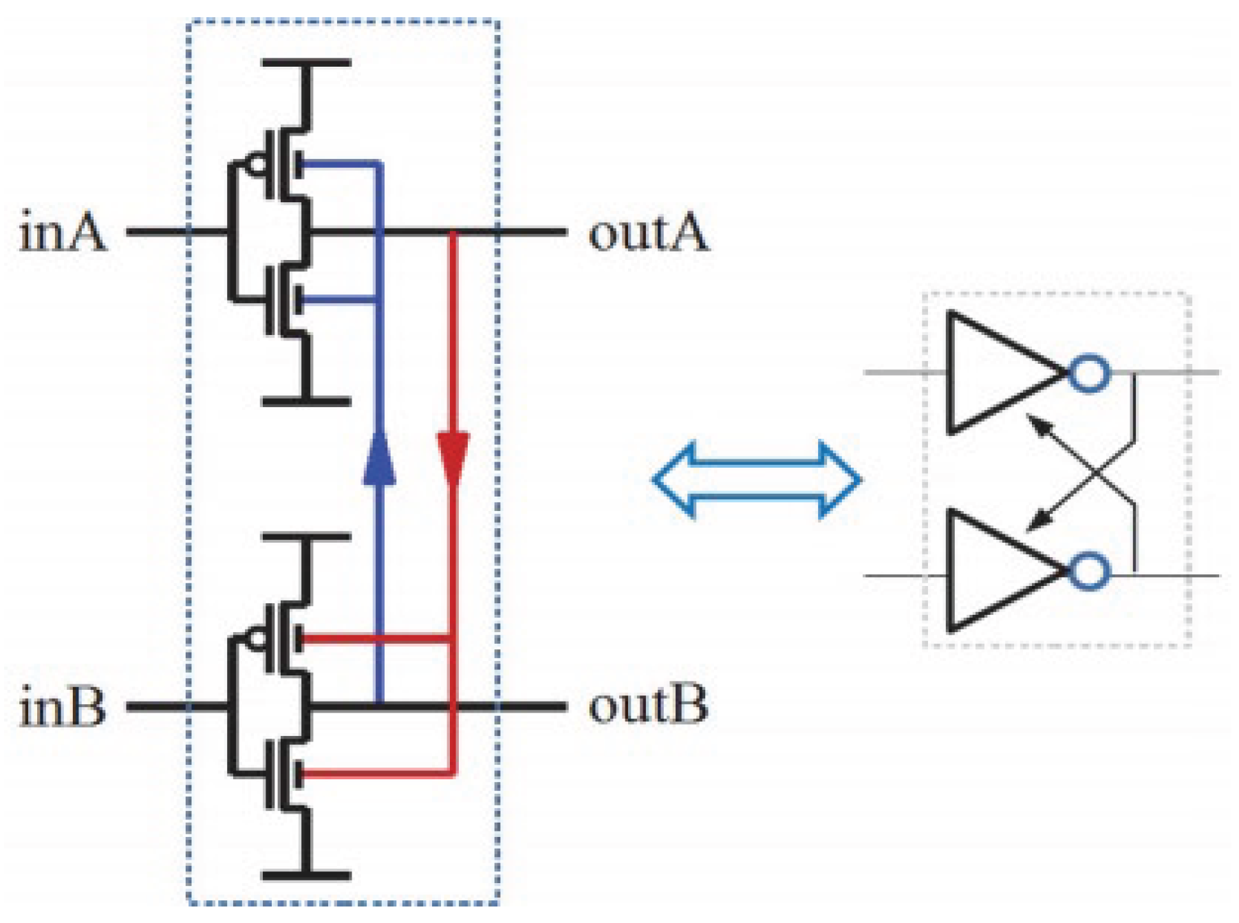
Figure 10.
Tuning range versus free-running frequency.
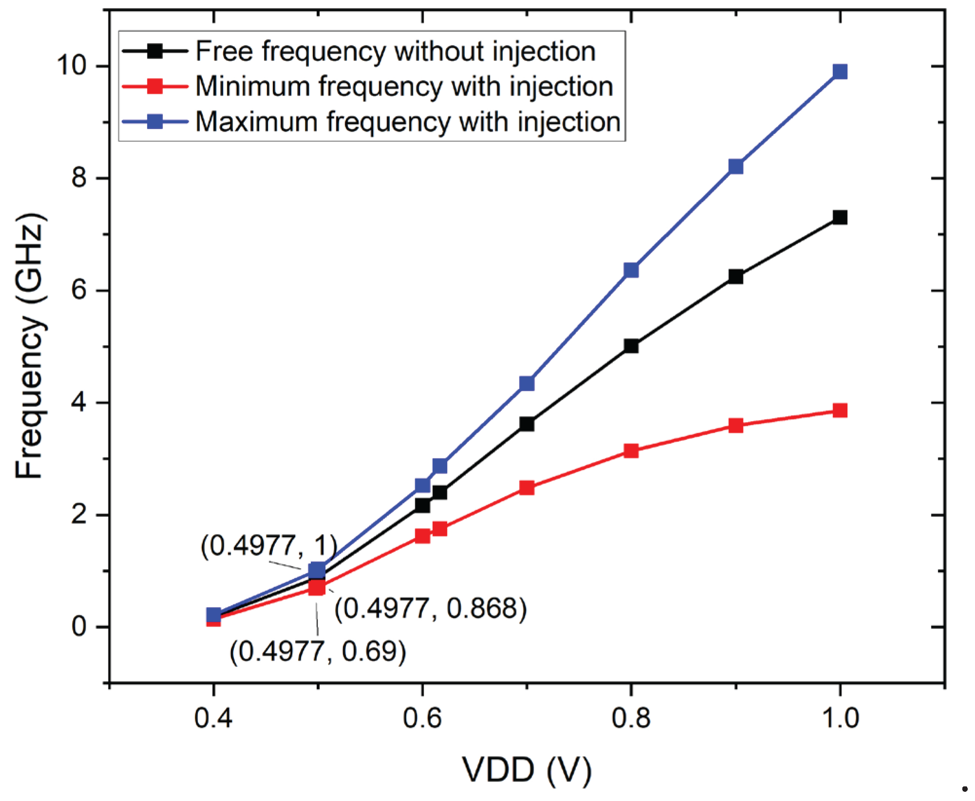
Figure 11.
Comparison of phase noise as a function of relative frequency.
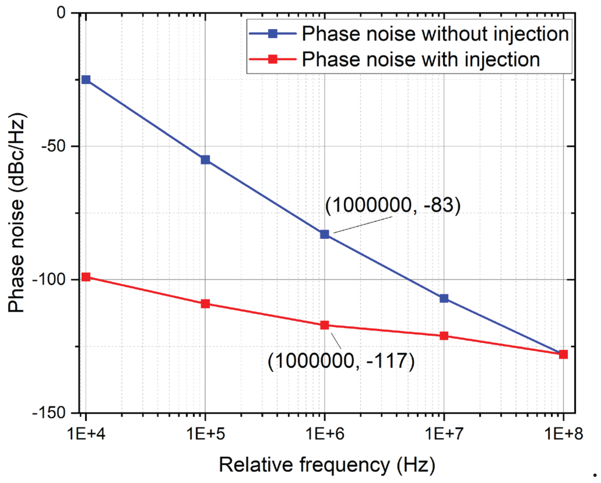
Figure 12.
Simplified block diagram of the proposed ILCDR.
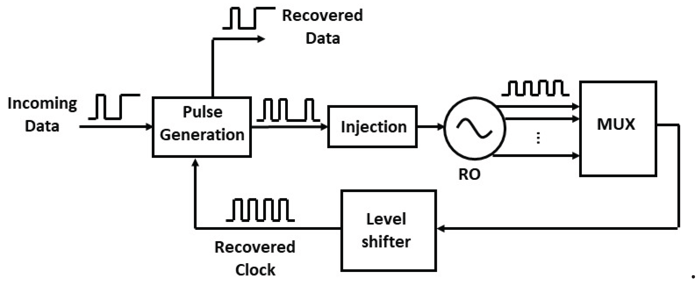
Figure 13.
Timing diagram of the proposed ILCDR.
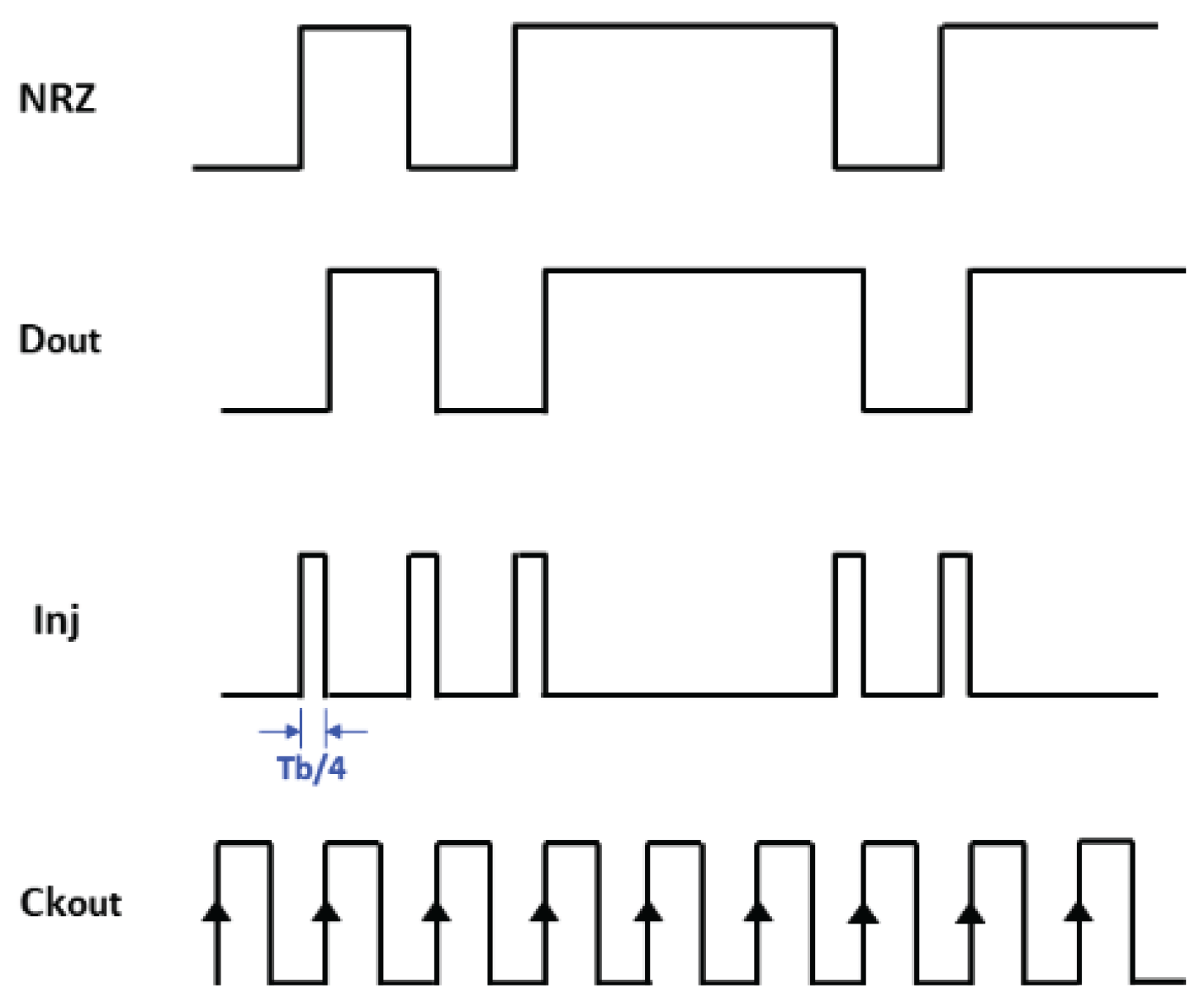
Figure 14.
Architecture of the proposed ILCDR (DFF clocked by CKOUT in blue).
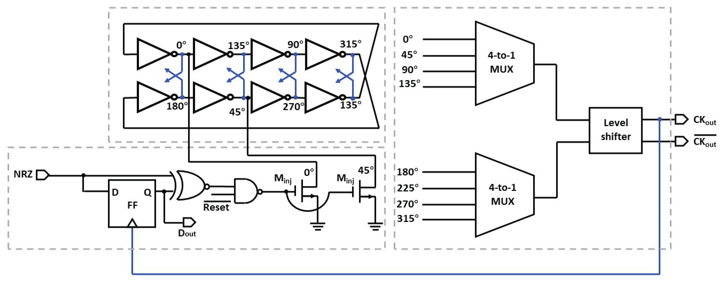
Figure 15.
Transient simulation result of complementary ILCDR at 868MHz.
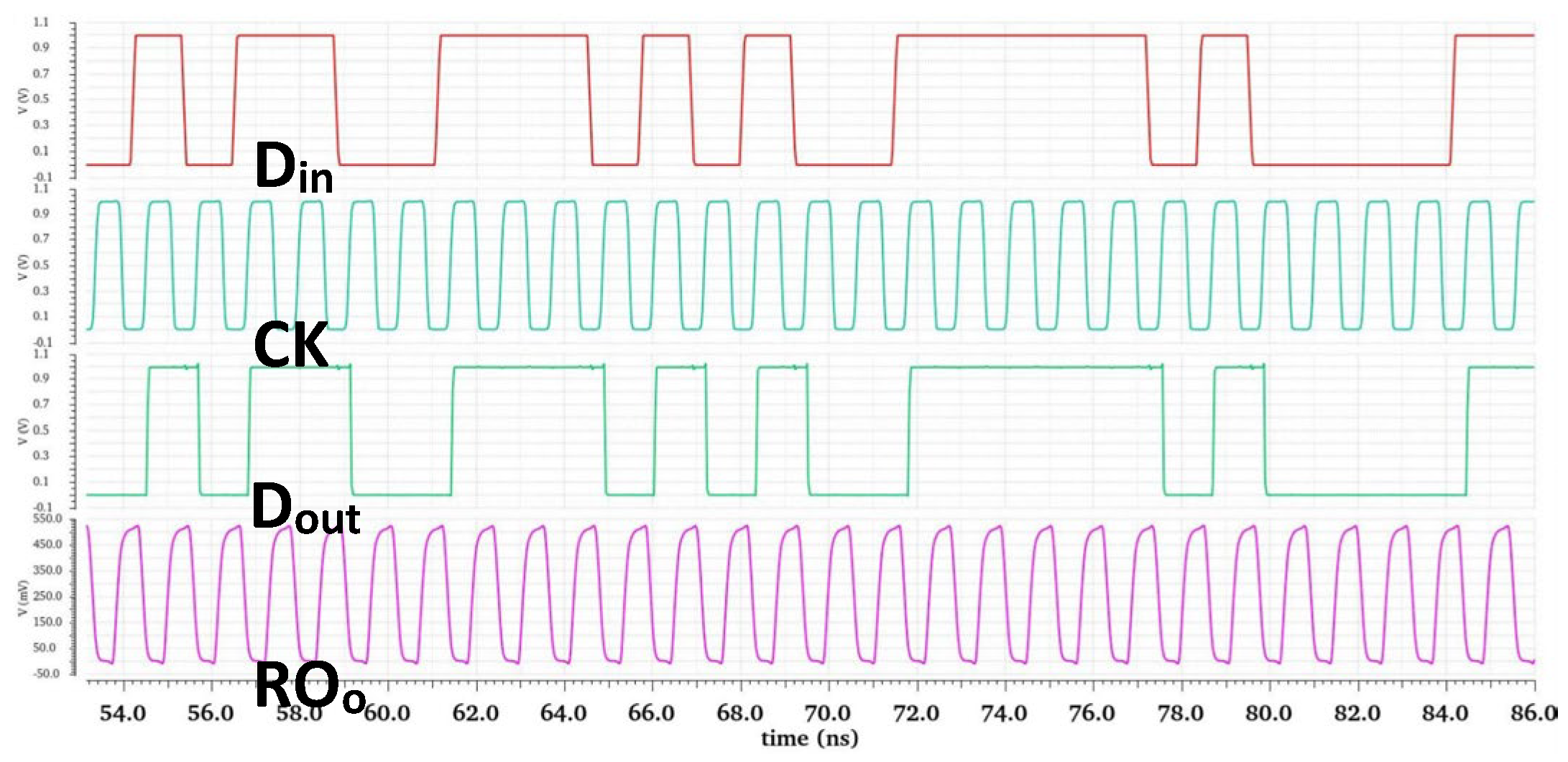
Figure 16.
Frequency of clock signal at 868MHz.
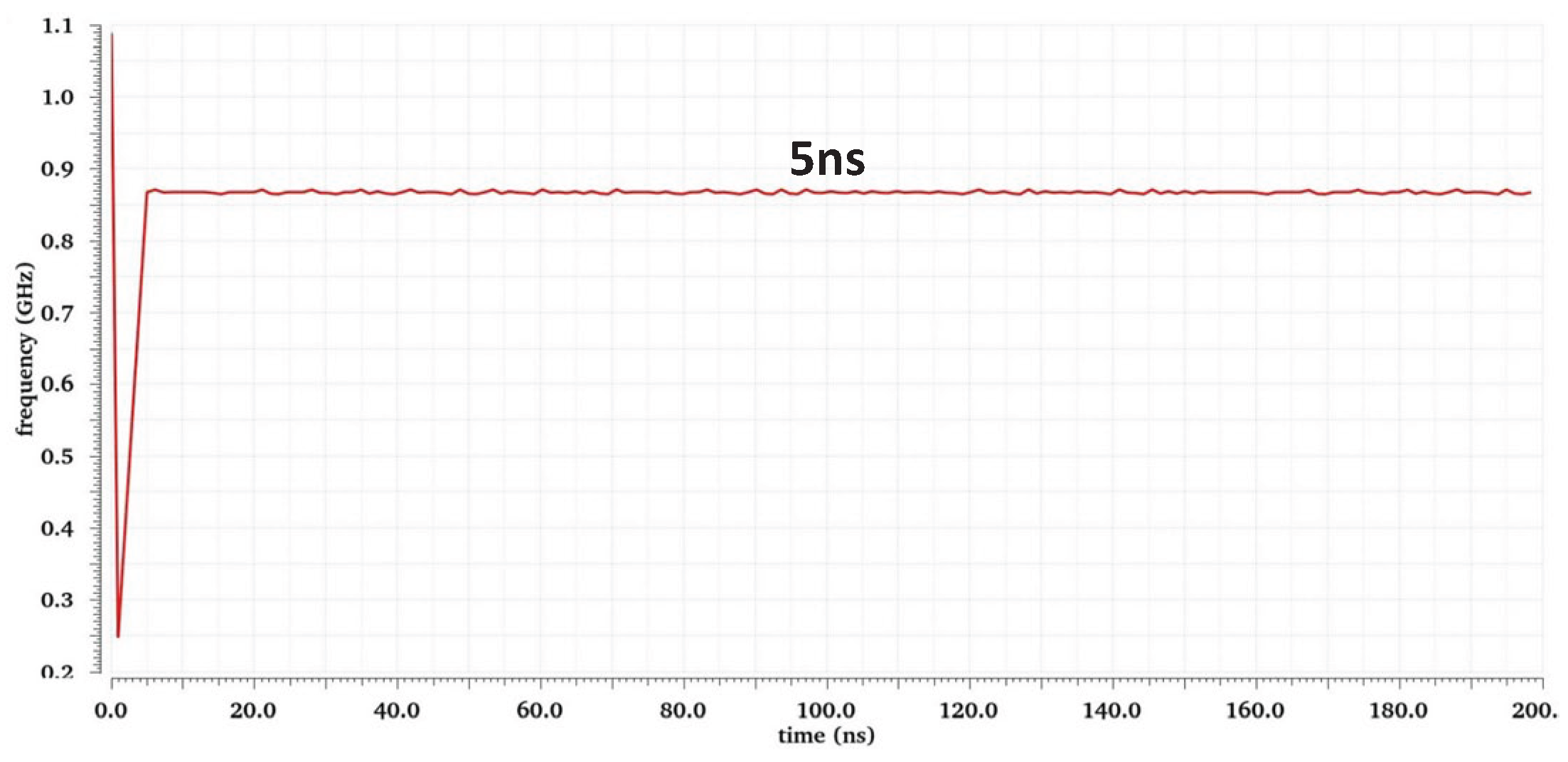
Figure 17.
Eye diagram of (a) Recovered clock (b) Recovered data.
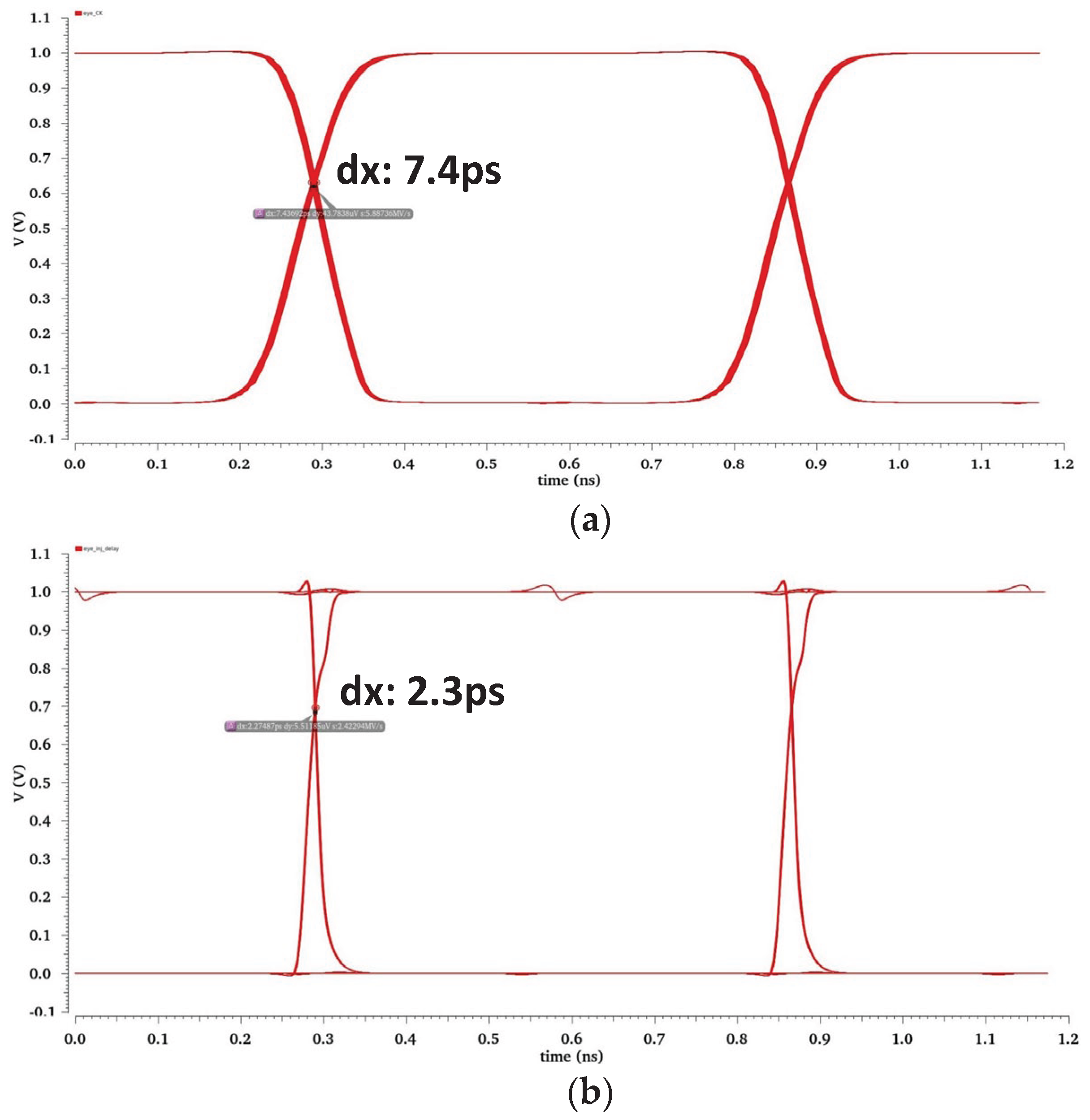
Figure 18.
Phase noise of CDR as a function of relative frequency.
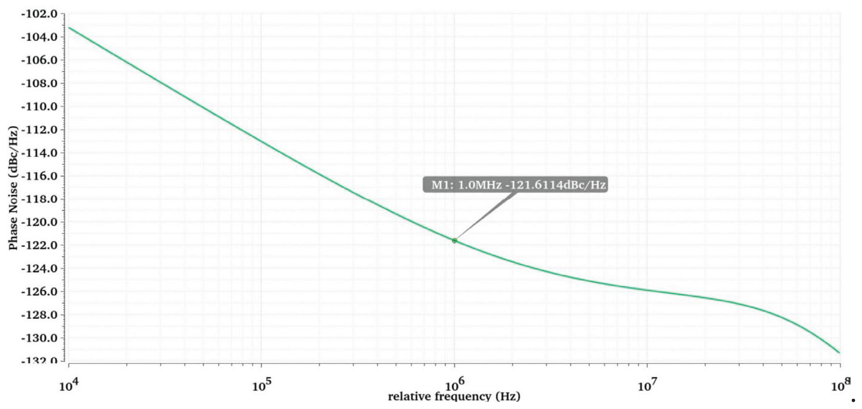
Figure 19.
Percentage of power consumption of each part of the circuit.

Figure 20.
Monte Carlo result of clock frequency at 868MHz with N=500.
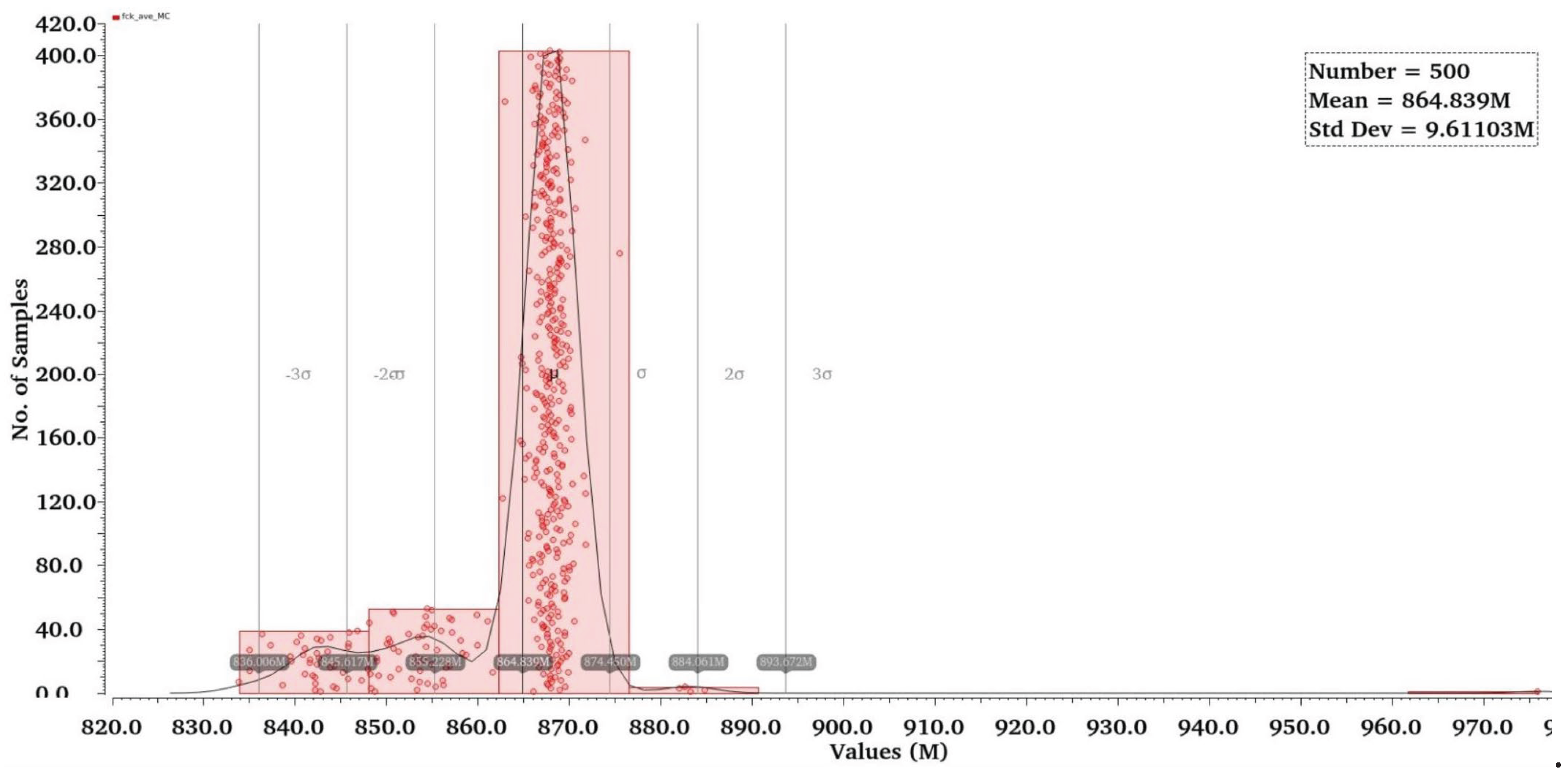
Figure 21.
Layout topology of one complementary inverter.
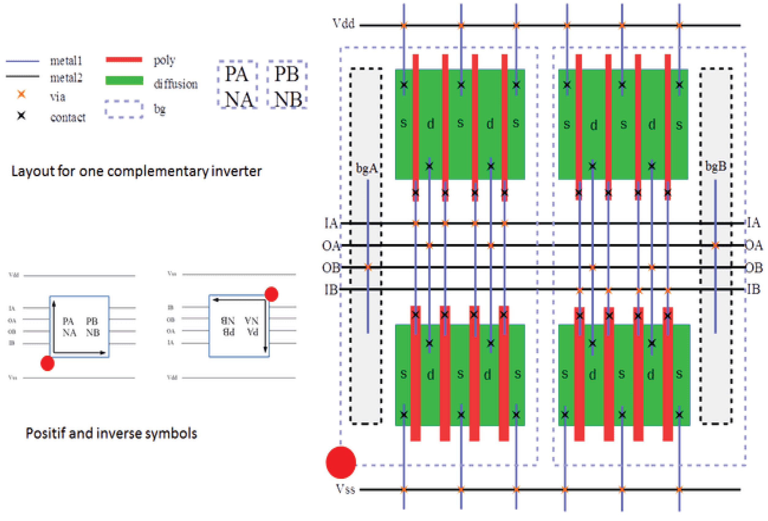
Figure 22.
Layout design of complementary inverter (8*8μm2).
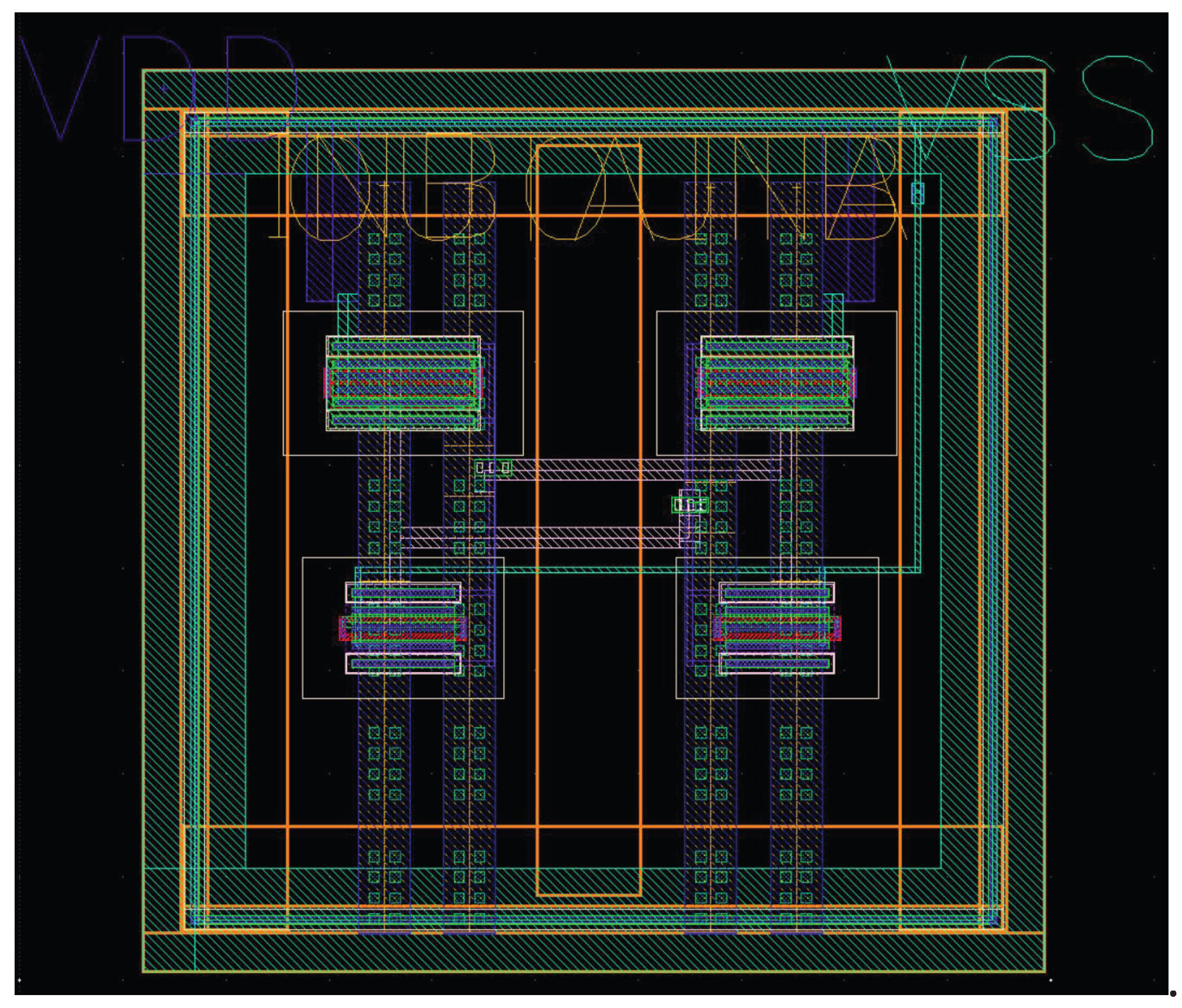
Figure 23.
Layout topology of one complementary RO.
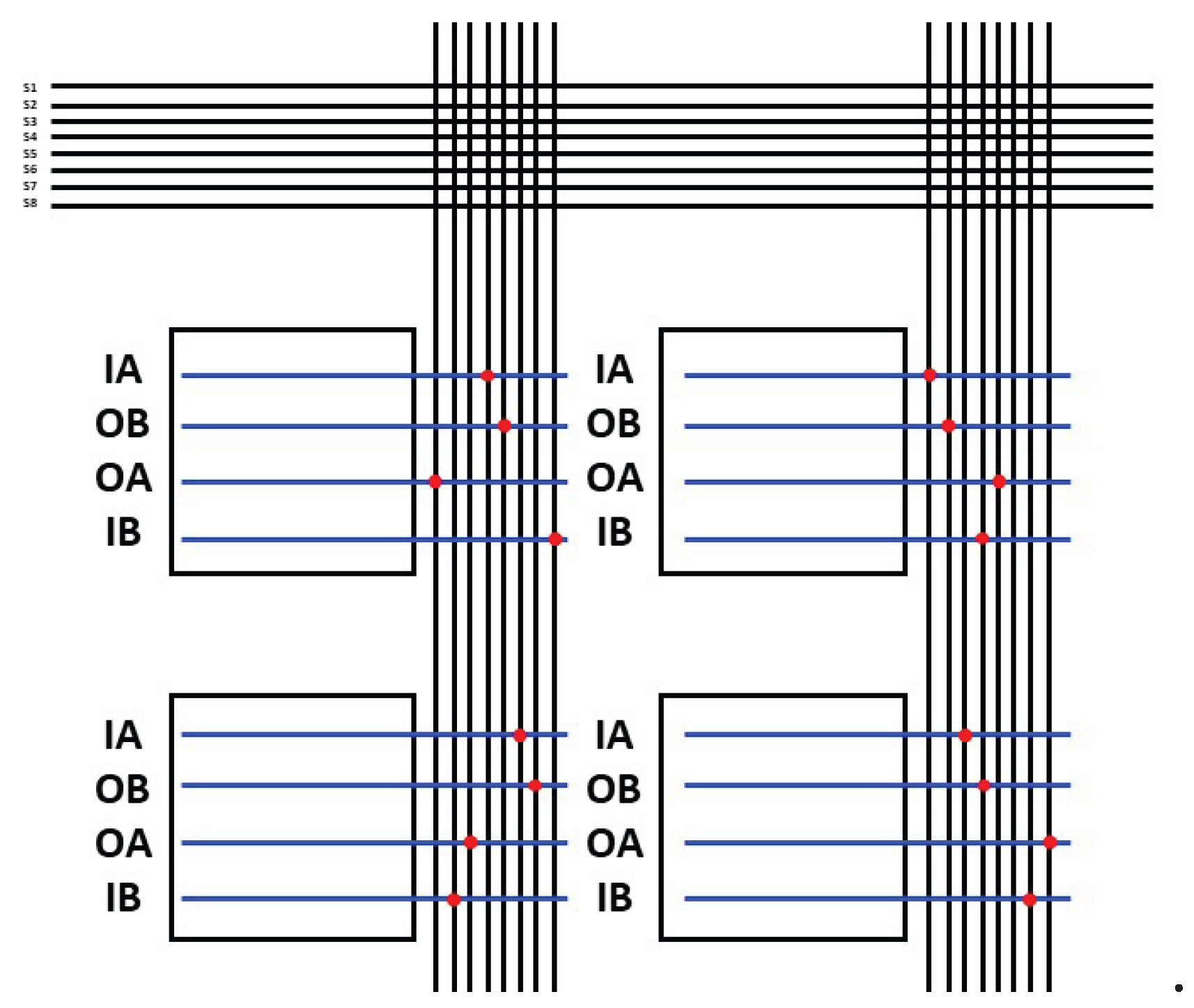
Figure 24.
Layout design of complementary RO (40*30μm2).
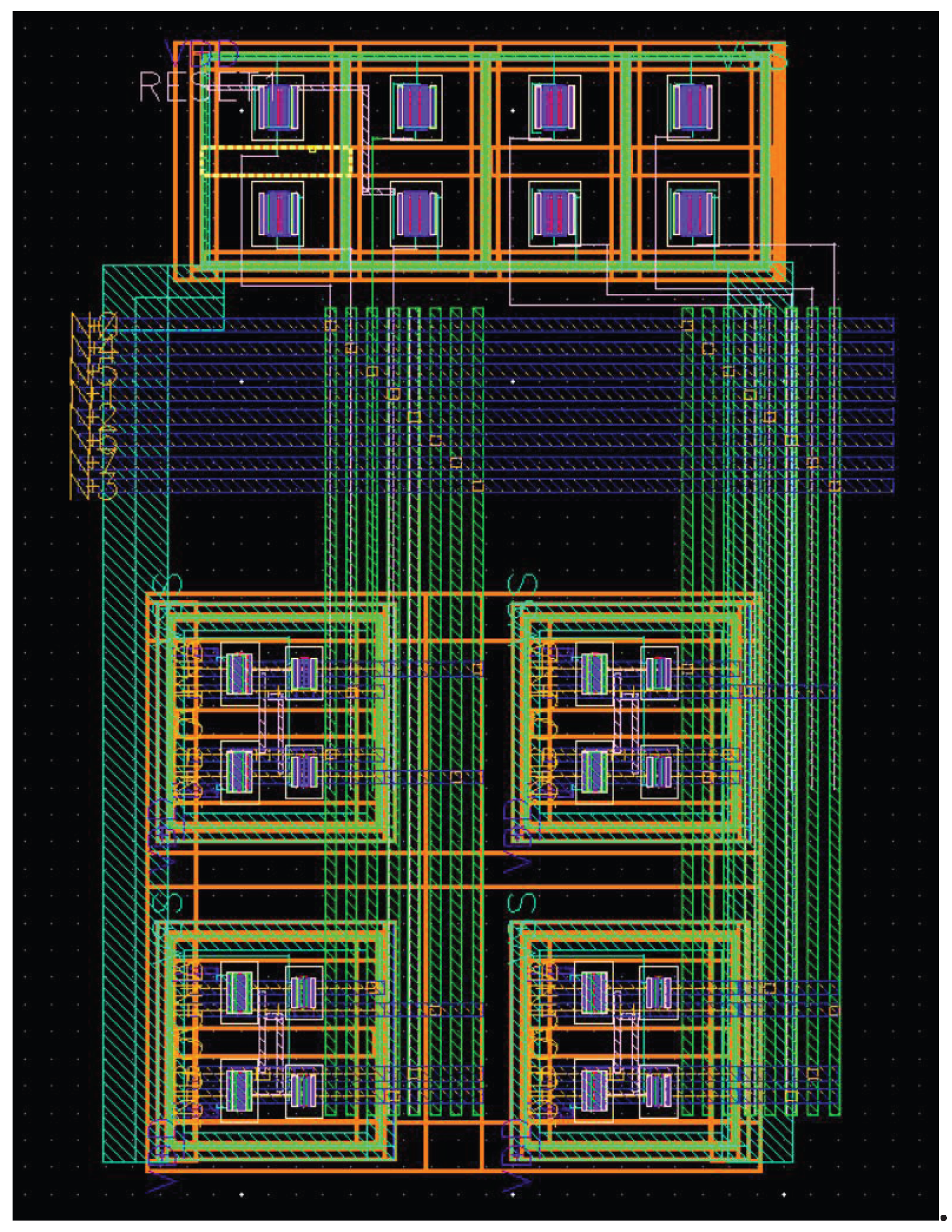
Figure 26.
Transient simulation results for complementary RO.
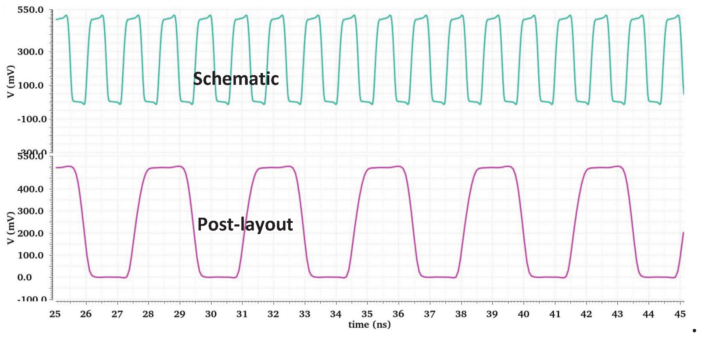
Figure 27.
Eye diagram of (a) Recovered clock (b) Recovered data.
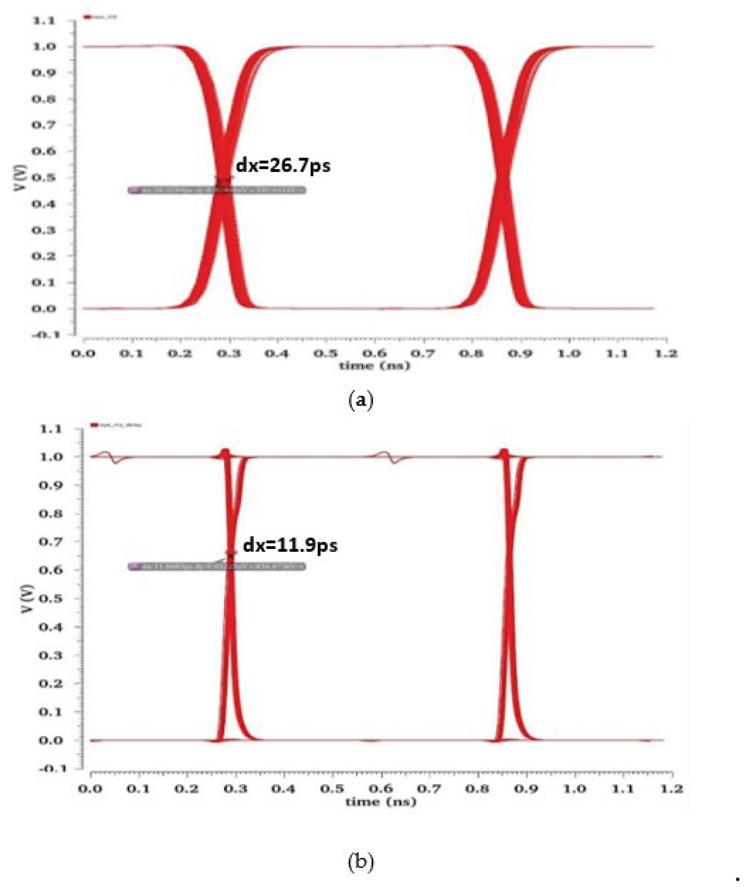
Table 1.
Output frequency (GHz) of complementary ILCDR at different process corners and temperatures with 868Mbps PRBS7 input data.
Table 1.
Output frequency (GHz) of complementary ILCDR at different process corners and temperatures with 868Mbps PRBS7 input data.
| Process | VDD (V) | Temperature (°C) | Ouput frequency (GHz) |
|---|---|---|---|
| TT | 0.5 | 27 | 0.868 |
| 0.5 | 125 | 1.45 | |
| 0.5 | -40 | 0.548 | |
| FF | 0.5 | 27 | 1.09 |
| 0.5 | 125 | 1.73 | |
| SS | 0.5 | 27 | 0.712 |
| 0.5 | -40 | 0.425 |
Table 3.
Output frequency of complementary ILCDR at different process corners and temperatures with 868Mbps PRBS7 input data.
Table 3.
Output frequency of complementary ILCDR at different process corners and temperatures with 868Mbps PRBS7 input data.
| TT, 27°C (Typical) |
FF, 27°C | FF, 125°C (Fastest) |
SS, 27°C | SS, -40°C (Slowest) |
|
| Schematic | 868MHz | 1.09GHz | 1.73GHz | 712MHz | 425MHz |
| Post-layout | 868MHz | 1.03GHz | 1.245GHz | 757MHz | 595MHz |
Table 4.
CDR performance summary and comparison.
| [20] | [21] | [22] | [23] | [24] | This work | |
| Technology (nm) | 28 | 28 | 40 | 28 | 180 | 28 |
| Architecture | Half rate | Half rate | Half rate | Half rate | Full rate | Full rate |
| CDR Type | PLL | Injection | PLL | PLL | Injection | Injection |
| Supply Voltage (V) | 1.0 | 0.9 | 1.2 | 1.0 | 1.8 | 0.6 |
| Data rate (Gbps) | 10 | 10 | 50 | 20 | 3.2 | 0.868 |
| p-p Jitter (ps) | 8.8 | 26.8 | 1.6 | N/A | 6.4mUI | 26.7 |
| Power Dissipation (mW) | 33 | 12.8 | 450 | 21.5 | 34.6 | 0.318 |
| Power efficiency (pJ/bit) | 3.3 | 1.28 | 9 | 1.08 | 10.81 | 0.37 |
| Core area (mm2) | 0.48 | 0.03 | N/A | N/A | 0.10 | 0.0012 (RO) 0.0066 (CDR)* |
* Estimated value.
Disclaimer/Publisher’s Note: The statements, opinions and data contained in all publications are solely those of the individual author(s) and contributor(s) and not of MDPI and/or the editor(s). MDPI and/or the editor(s) disclaim responsibility for any injury to people or property resulting from any ideas, methods, instructions or products referred to in the content. |
© 2024 by the authors. Licensee MDPI, Basel, Switzerland. This article is an open access article distributed under the terms and conditions of the Creative Commons Attribution (CC BY) license (http://creativecommons.org/licenses/by/4.0/).
Copyright: This open access article is published under a Creative Commons CC BY 4.0 license, which permit the free download, distribution, and reuse, provided that the author and preprint are cited in any reuse.


