
Submitted:
18 January 2024
Posted:
19 January 2024
You are already at the latest version
Abstract
The rapid development of electric vehicles, unmanned aerial vehicles, and wearable electronic devices has led to a high interest in research related to the synthesis of graphene with a high specific surface area for energy applications. However, the problem of graphene synthesis scalability, as well as the lengthy duration and high energy intensity of the activation processes of carbon materials, are significant disadvantages. In this study, a reactor was developed for the green, simple, and scalable electrochemical synthesis of graphene oxide with a low oxygen content of 14.1 %. The resulting material was activated using a fast joule heating method. The processing of mildly oxidized graphene with a high–energy short electrical pulse (32 ms) made it possible to obtain a graphene–based porous carbon material with a specific surface area of up to 1984.5 m2/g. The low energy intensity, simplicity, and use of environmentally friendly chemicals render the proposed method scalable.
Keywords:
graphene
; mildly oxidized graphene
; electrochemically exfoliated graphene
; fast joule heating
; activated carbon
; specific surface area
1. Introduction
Porous carbon materials (PCMs), owing to their structural features and chemical properties, have a wide range of applications [1] and have attracted significant attention from the scientific community [2]. The development of methods for fast, environmentally friendly, and cheap production of PCMs is especially relevant in connection with the rapid development of the energy industry for electric vehicles, unmanned aerial vehicles, and wearable electronics devices. Recently, great progress has been made in the production of synthetic carbon nanomaterials such as carbon nanotubes and graphene materials [3]. Due to their high thermal and electrical conductivities, these materials are considered more promising for use in power supplies with high power densities [4]. A large amount of research has been carried out on the use of graphene–based materials for the production of PCMs. [2]. Research related to graphene oxide (GO) has received much attention owing to the low cost of its production, as well as the possibility of flexible modification [5]. GO is an oxidized form of graphene that contains a large number of functional groups in various configurations [6]. The GO is an electric insulator [6]. The electrical conductivity of GO can be significantly increased by reduction, which removes oxygen functional groups [7]. Various methods for GO reduction have been proposed, such as thermal annealing [8], laser annealing [9], and microwave irradiation [10]. In terms of scalability, chemical methods using reducing agents such as hydrazine (N2H4) [11] and sodium borohydride (NaBH4) [12] have been well established. However, chemical reduction requires lengthy treatment times, leads to contamination of the GO by the reducing agent, and is often performed using toxic and hazardous agents [13]. In addition, the high content of oxygen groups in the GO makes deep reduction problematic, which negatively affects the electrical conductivity. Methods for the synthesis of mildly oxidized graphene (MOG), such as electrochemical exfoliation [14], are of great interest. This method makes it possible to obtain GO with a low oxygen content of up to 20 % [14], compared to 50 % for GO obtained using classical methods [6]. In addition, electrochemical exfoliation can significantly reduce the synthesis time and is highly scalable. It can also be performed using non–toxic materials with high water solubility, which contributes to environmental friendliness and improves the purity of the product. However, this method has some major shortcomings. The main disadvantage is the exfoliation of large graphite particles during synthesis [15]. When detached from the graphite electrode, these particles do not participate in the electrochemical process and reduce the yield of the few–layer graphene flakes. Also, during swelling and oxidation of the original electrode, an uneven distribution of the electric field occurs in the volume of the electrode [16]. In addition, the molding of graphite electrodes is a separate technological step, in which various impurities in the form of various binders and contaminants can be introduced. To solve these problems, Achee et al. [15] proposed electrochemical exfoliation in a contained volume. The authors used a dialysis bag containing an electrode and a graphite powder. The use of a contained volume made it possible to increase the yield to 65 %, as well as the quality of the resulting MOG. In addition, a scalable flow reactor prototype was proposed. However, in the proposed design it is impossible to stir the graphite powder to ensure uniform processing of the entire volume.
The next technological step in the PCMs production is the activation process [17]. Upon activation, a micro– and nanoporous structure is created. This allows for high specific surface area, helping to increase adsorption or specific energy density in energy applications [18]. The most common methods for activating carbon materials are chemical and physical activations [17]. Both methods involve lengthy thermal treatment of the original carbon precursor with a strong alkali solution, such as KOH [17]. The main disadvantages of these methods are their high energy intensity, process duration, and the use of dangerous chemicals [17,18]. Recently, research on methods for processing carbon materials using fast joule heating has gained high interest [19]. This method can be used to activate oxidized carbon materials [20]. The fast joule heating technique involves the rapid reduction of oxidized material during flash–heating, associated with a large discharge current. The intense release of oxygen groups occurs in the form of gaseous products, which leads to the formation of pores when the graphene flakes rupture [20]. For the application of this method, MOG is more suitable due to its electrical conductivity, in contrast to GO obtained by the Hummers method, which is a dielectric material. In [20], the authors coated carbon fabric with a layer of GO. Electrical pulses with a duration of 50 ms were then applied to the fabric at a voltage of 30 V. After treatment with 20 pulses, the specific surface area of composite material increased to 166 m2/g. By mixing the initial GO with KOH, the specific surface area increased to 974 m2/g. In [21], carbon fibers were activated via fast joule heating. It was shown that when pulses of 4 to 8 V were applied, pores formed on the surface of the fibers. Increased specific surface area had a positive effect on the electrochemical performance of the treated material. However, the specific surface area was not analyzed in this study. To the best of our knowledge, activation by fast joule heating has only been investigated in these studies, making additional research in this area relevant.
In this study, a novel reactor was developed for the electrochemical exfoliation of graphite in a closed, expandable volume, which addressed the issue of large particle exfoliation. The proposed reactor design also provides the possibility of stirring the processed powder to increase the uniformity of exfoliation. To activate the MOG, a fast joule heating setup was developed, and optimal parameters were selected to maximize the increase in specific surface area. This study presents a cost–effective and green method for quick production of PCMs with a high specific surface area, without the use of chemical processing. Additionally, fast joule heating resulted in simultaneous reduction of MOG and increase in electrical conductivity. The BET method was used to study the specific surface area, revealing a substantial increase in the specific area of MOG after processing in the fast joule heating installation.
2. Materials and Methods
The synthesis of MOG was carried out in a reactor with two sealed volumes positioned vertically to one another and separated by a semi–permeable polyethylene terephthalate membrane with 1 µm pores (Figure 1). The upper volume served as a container for the electrolyte and was equipped with a gold electrode. A 0.1 M solution of Na2SO4 (Rushim, Moscow, Russia) was used as an electrolyte. The lower volume was equipped with a movable piston with a gold electrode was fixed to its surface.
The graphite powder has been processed through a number of steps. First, 2 g of flake graphite from Sigma Aldrich (St. Louis, MO, USA) were placed in a lower volume, which periodically replenished electrolyte and mixed graphite powder by moving the piston. A positive voltage of +10 V was applied to the graphite, causing it to oxidize and exfoliate, resulting in a volume increase of the original graphite powder. The exfoliation process took 6 h, after which the small particles of oxidized graphite were collected for further treatment. The obtained product was then rinsed using a vacuum filtration unit with a copious amount of deionized water. The resulting dry residue was mixed with 100 ml of deionized water to form an aqueous suspension of oxidized graphite. The suspension was treated with ultrasound at 60 W for 3 h using an Up 200St installation (Hielscher Ultrasonics, Teltow, Germany), resulting in the peeling of oxidized graphite particles and the formation of a suspension of few–layer MOG. The MOG suspension was then centrifuged at 14,500 rpm for 10 min to separate the unexfoliated particles by decanting the over the sediment.
To activate the MOG, the methodology outlined in previous study [22] and he studies discussed in [19] was employed. A 32 mF capacitor bank was charged to the required value and then discharged into the reaction chamber at voltages ranging from 100 to 220 V. The reaction chamber consisted of copper electrodes that pressed the MOG powder in a quartz tube with a diameter of 14 mm. The discharge occurred in a nitrogen atmosphere at a pressure of 0.3 mbar and took approximately 32 ms. The activated material was labeled activated MOG (aMOG), and the samples corresponding to the processing voltages were aMOG–100, aMOG–140, aMOG–180, aMOG–200, and aMOG–220.
The Raman spectra of the resulting material were examined using the NTegra Spectra installation (NT–MDT, Zelenograd, Russia). The surface morphology of the resulting material was analyzed using scanning electron microscopy (SEM) with a JEOL–7800F microscope (Jeol, Tokyo, Japan). Atomic force microscopy (AFM) was employed to study the individual MOG and aMOG flakes using Solver Next (NT–MDT, Zelenograd, Russia). The elemental composition was determined using X–ray energy dispersive spectroscopy (EDS) with a NanoAnalysis microanalysis system (Oxford Instruments, Oxford, UK) attachment of the SEM. The functional composition was studied through Fourier transform infrared spectroscopy (FTIR) with a Spotlight 200i spectrometer (PerkinElmer, Waltham, MA, USA). Measurements of current–voltage characteristics (C–V) were performed using a two–probe method on ASEC–03 (Prokhorov General Physics Institute of the Russian Academy of Sciences, Moscow, Russia) and AMM–3046 (Aktakom, Moscow, Russia) in the voltage range of -1 to +1 V. The specific surface area was determined using the Brunauer–Emmett–Teller method on NOVAtouch LX (Quantachrome Instruments, Inc., Boynton Beach, FL, USA) with a static volumetric method to measure the amount of adsorbed nitrogen. The preparation of the samples was carried out in accordance with the ISO 9277:2010 standard. The samples were degassed at a residual pressure of 10 μT and a degassing temperature of 350 °C for 12 h. The free space (“dead volume”) of the cells was initially determined using helium. The purities of N2 and He were > 99.999 %.
3. Results
Figure 2 shows AFM images of the initial MOG (a) and aMOG–200 (b) individual flakes. Thickness profiles are displayed in each image. The average lateral dimensions of individual MOG flakes were in the range between 0.05 and 0.8 µm, with thicknesses varying between 6 and 20 nm. In comparison, the lateral dimensions of the aMOG–200 flakes were within 100 nm, with thicknesses of 0.8 to 1.2 nm. On average, individual flakes of MOG exhibit a greater number of graphene layers than aMOG–200, and also larger lateral dimensions. This indicates that the initial MOG flakes underwent rupture during the activation process with fast joule heating.
Images of the MOG and aMOG–200 films surfaces were obtained using the SEM (Figure 3). It is shown that the MOG film consists of agglomerated particles formed during the drying of the MOG suspension. The surface of aMOG–200 has a micro– and nanoporous structure formed as a result of activation.
The elemental analysis of the initial MOG and aMOG–200 are presented in Table 1. It should be noted that the EDS did not allow the identification of hydrogen atoms. The data indicates that the developed reactor successfully synthesized MOG with a notably low oxygen content of 14.1 %. MOG was reduced by rapid joule heating to an oxygen content of 4.2 %.
Figure 4a shows the FTIR–spectra of the MOG and aMOG–220. The peak localized in the vicinity of 1250 cm–1 corresponds to O–H hydroxyl group [23,24]. Presence of the hydroxyl group were confirmed by the presence of vibrations in the region of 3200–3400 cm–1, also associated with O–H groups and H2O [24]. The peak associated with stretching vibrations of carboxyl groups (–COOH) is observed in the region of 1725 cm–1. The disturbances localized in the vicinity of 1091 cm–1, associated with the presence of epoxy groups (C–O–C). Stretching vibrations of C–O bonds of hydroxyl groups in the region of 1044 cm–1 is present [23]. It is worth noting that for aMOG, the C–O bonds (1131 cm–1) associated with hydroxyl groups [23,24] were absent. The presence of C=C bonds are also observed (1680–1710 cm–1), which are related to the vibrations of sp2–crystallites of graphite [23,24].
Figure 4b shows the Raman spectra of MOG and aMOG–220 samples obtained after joule heating. All powders were characterized by the presence of the main peaks, D (1350 cm–1) and G (1580 cm–1), corresponding to graphite and graphene–containing structures [25]. Raman spectra of MOG samples demonstrate the presence of a wide band 2D–peak in the region of 2700–3100 cm–1. After the fast joule heating, the Raman spectra of aMOG–220 changed significantly. The D–peak intensity decreased. Clearly defined peak at 2701 cm–1, corresponding to the second–order 2D–peak was observed [26]. The intensity of 2D–peak shows graphitization of the initial MOG, which, coupled with the low intensity of the D–peak and sharp G–peak, indicates the formation of ordered graphene flakes [27].
The Raman spectra of aMOG obtained under various discharge voltages are shown in Figure 5a. Peaks corresponding to graphite and graphene–containing structures (D, G, 2D, and D+G) were identified [28]. As can be seen from Figure 5a, the peak at 3150 cm–1 disappears with increasing voltage. This peak corresponds to the hydroxyl and carbon–hydrogen groups [29]. An increase in the energy of discharge contributes to removal of peaks localized in the frequency range 2900, 3100 cm–1. Figure 5b shows the decomposition of the Raman spectra of aMOG–220 into Lorentzian peaks. The ratio of the integrated peak intensities (ID/IG), which is responsible for assessing the disorder of the carbon structure, is 0.45, which corresponds to the defective graphene [30]. From the empirical formula [31] defined by Cancado et al., the lateral dimensions of sp2–crystallites of nanographite were calculated (Table 2). The ratio of I2D/IG shows that the aMOG–220 is close to few–layer graphene. The estimate at the first approximation was up to 7 layers [32], which correlates with the data obtained by the AFM method.
Table 2 shows the values of the surface resistance (R/sq.) of the aMOG, obtained from measurements of C–V characteristics using the two–probe method.
Figure 6 shows the average values of the surface resistance depending on the treatment voltage. It can be seen that with increasing voltage, R decreases from the initial values (from the insulator) to tens of Ω/sq., indicating the reduction of MOG and regeneration of graphene structure. Which is confirmed by the growth of sp2–crystallites La. Due to the high degree of disorder in the initial MOG and aMOG–100, La was not assessed. With an increase in the lateral dimensions of the sp2–crystallites, the electrical conductivity of aMOG increased by up to four orders of magnitude.
The specific surface areas measured using the BET method are listed in Table 3. From the calculated values, it can be concluded that with increasing in discharge voltage, the specific surface area also increases to a maximum at 200 V — 1984.5 m2/g. However, at the discharge voltage of 220 V, a sharp decrease in the surface area was observed.
BET studies showed that the adsorption isotherms for all samples, according to the IUPAC classification, belong to type IV. The hysteresis loops in all isotherms are of H1 type, which are characteristic of agglomerates of spherical particles that are uniformly packed and similar in size. The nature of the adsorption branches at low relative pressures indicated the presence of a certain number of micropores. All the samples exhibited a multimodal distribution of pore volume and size. The distribution of the pores by volume of the aMOG–200 with highest measured specific surface area is presented in Figure 7.
4. Discussion
The results obtained from the data indicate that the reactor developed in this study can produce multilayer flakes of MOG with an oxygen content of up to 14.1 %. The composition of the functional groups of the initial MOG correlates with data obtained in other studies [14]. At the same time, reactor design has the possibility of significant scaling. The use of the fast joule heating method made it possible to increase the conductivity of aMOG by four orders of magnitude, which can be associated with the thermal reduction of the initial MOG to an oxygen content of 4.2 %. Simultaneously, the explosive release of oxygen groups in the form of gaseous products during fast joule heating (32 ms) led to the rupture of individual flakes of the initial MOG [20]. AFM studies showed a decrease in lateral dimensions from 0.8 μm to 100 nm and thicknesses from 6–20 nm to 0.8–1.2 nm for aMOG, compared to the initial MOG. This explains the significant increase in the specific surface area of aMOG–200 to 1984.5 m2/g at a processing voltage of 200 V. The hysteresis loops of the adsorption isotherms of the material are of type H1, which are characteristic of agglomerates of spherical particles that are uniformly packed and similar in size. At the same time, Raman spectra shows a decrease in the D–peak associated with structural defects. This indicates that during the activation by fast joule heating, percolation did not occur in the lateral plane of the flakes. The data obtained from the BET analysis indicates a significant increase in the specific surface area as the processing voltage was increased, to a maximum area at 200 V. At the processing voltage of 220 V, a significant relative decrease in the specific area was observed. It can be speculated that this effect may be associated with a regeneration of the sp2 structure, which leads to the restacking of individual flakes via the Van–der–Waals forces. Which is indirectly confirmed by the high electrical conductivity of aMOG–220 (~20 Ω/sq). Additional research is needed to establish the reasons for this effect.
In conclusion an original reactor was developed for the electrochemical synthesis of MOG. The synthesis of MOG was carried out without the use of toxic and dangerous reagents and also has low energy intensity, which is the basis for possible scalability. To activate synthesized MOG and obtain the graphene–based PCMs, fast joule heating was used. This method made it possible to obtain graphene–based PCMs with a high specific surface area of up to 1984.5 m2/g. Due to its speed, simplicity, and low energy consumption, the developed technique can be used for green production of PCMs for various energy sources such as Li–ion batteries and supercapacitors.
Author Contributions
Conceptualization, Z.I.E. and A.R.P.; methodology, Z.I.E., A.R.P., N.N.L. and D.N.P.; validation, Z.I.E. and A.R.P.; investigation, Z.I.E., A.R.P., P.S.D., N.N.L. and D.N.P.; writing—original draft preparation, Z.I.E., A.R.P. and P.S.D.; writing—review and editing, Z.I.E., A.R.P. and P.S.D. All authors have read and agreed to the published version of the manuscript.
Funding
This research was funded by the Ministry of Education and Science of the Russian Federation (the state tasks FSRG–2022–0011).
Institutional Review Board Statement
Not applicable.
Informed Consent Statement
Not applicable.
Data Availability Statement
The data presented in this study are available upon request from the corresponding author. The data are not publicly available due to the data protection policy of the university.
Acknowledgments
We thank Vinokurov P.V. for his help with the AFM and Raman–spectra measurements.
Conflicts of Interest
The authors declare no conflict of interest. The funders had no role in the design of the study; in the collection, analyses, or interpretation of data; in the writing of the manuscript, or in the decision to publish the results.
References
- Liu, P.; Chen, G.-F. Applications of porous ceramics. In Porous Materials Processing and Applications, 1st ed.; Elsevier Inc.: Amsterdam, The Netherlands, 2014; pp. 303–344. [Google Scholar]
- Huang, H.; Shi, H.; Das, P.; Qin, J.; Li, Y.; Wang, X.; Su, F.; Wen, P.; Li, S.; Lu, P.; et al. The chemistry and promising applications of graphene and porous graphene materials. Adv. Funct. Mater. 2020, 30, 1909035. [Google Scholar] [CrossRef]
- Wang, Y.; Chen, J.; Ihara, H.; Guan, M.; Qiu, H.D. Preparation of porous carbon nanomaterials and their application in sample preparation: A review. TrAC Trend. Anal. Chem. 2021, 143, 116421. [Google Scholar] [CrossRef]
- Han, J.; Johnson, I.; Chen, M. 3D continuously porous graphene for energy applications. Adv. Mater. 2022, 34, 2108750. [Google Scholar] [CrossRef] [PubMed]
- Hooch Antink, W.; Choi, Y.; Seong, K.D.; Kim, J.M.; Piao, Y. Recent progress in porous graphene and reduced graphene oxide-based nanomaterials for electrochemical energy storage devices. Adv. Mater. Inter. 2018, 5(5), 1701212. [Google Scholar] [CrossRef]
- Zhu, Y.; Murali, S.; Cai, W.; Li, X.; Suk, J.W.; Potts, J.R.; Ruoff, R.S. Graphene and graphene oxide: Synthesis, properties, and applications. Adv. Mater. 2010, 22, 3906–3924. [Google Scholar] [CrossRef] [PubMed]
- Pei, S.; Cheng, H. –M. The reduction of graphene oxide. Carbon 2012, 50, 3210–3228. [Google Scholar] [CrossRef]
- Alam, S.N.; Sharma, N.; Kumar, L. Synthesis of graphene oxide (GO) by modified hummers method and its thermal reduction to obtain reduced graphene oxide (rGO). Graphene 2017, 6, 1–18. [Google Scholar] [CrossRef]
- Huang, L.; Liu, Y.; Ji, L.C.; Xie, Y.Q.; Wang, T.; Shi, W.Z. Pulsed laser assisted reduction of graphene oxide. Carbon 2011, 49(7), 2431–2436. [Google Scholar] [CrossRef]
- Voiry, D.; Yang, J.; Kupferberg, J.; Fullon, R.; Lee, C.; Jeong, H.Y.; Shin, H.S.; Chhowalla, M. High–quality graphene via microwave reduction of solution–exfoliated graphene oxide. Science 2016, 353, 1413–1416. [Google Scholar] [CrossRef]
- Park, S.; An, J.; Potts, J.R.; Velamakanni, A.; Murali, S.; Ruoff, R.S. Hydrazine–reduction of graphite– and graphene oxide. Carbon 2011, 49, 3019–3023. [Google Scholar] [CrossRef]
- Shin, H.J.; Kim, K.K.; Benayad, A.; Yoon, S.; Park, H. Efficient reduction of graphite oxide by sodium borohydride and its effect on electrical conductance. Adv. Funct. Mater. 2009, 19, 1987–1992. [Google Scholar] [CrossRef]
- de Barros, N.G.; Gonzaga Neto, A.C.; Vaccioli, K.B.; Angulo, H.R.V.; de Andrade e Silva, L.G.; Toffoli, S.M.; Valera, T.S. Graphene Oxide: A Comparison of Reduction Methods. C 2023, 9, 73. [Google Scholar] [CrossRef]
- Vasilieva, F.D.; Kapitonov, A.N.; Yakimchuk, E.A.; Smagulova, S.A.; Antonova, I.V.; Kotin, I.A. Mildly oxidized graphene oxide suspension for printing technologies. Mater. Res. Express 2018, 5, 65608. [Google Scholar] [CrossRef]
- Achee, T.C.; Sun, W.; Hope, J.T.; Quitzau, S.G.; Sweeney, C.B.; Shah, S.A.; Habib, T.; Green, M.J. High–Yield Scalable Graphene Nanosheet Production from Compressed Graphite Using Electrochemical Exfoliation. Sci. Rep. 2018, 8, 1–8. [Google Scholar] [CrossRef] [PubMed]
- Muhsan, A.A.; Lafdi, K. Numerical study of the electrochemical exfoliation of graphite. SN Applied Sciences 2019, 1, 1–8. [Google Scholar] [CrossRef]
- Heidarinejad, Z.; Dehghani, M.H.; Heidari, M.; Javedan, G.; Ali, I.; Sillanpää, M. Methods for preparation and activation of activated carbon: A review. Environ. Chem. Lett. 2020, 18, 393–415. [Google Scholar] [CrossRef]
- Wang, G.; Yu, M.; Feng, X. Carbon materials for ion–intercalation involved rechargeable battery technologies. Chem. Soc. Rev. 2021, 50, 2388–2443. [Google Scholar] [CrossRef]
- Wyss, K.M.; Luong, D.X.; Tour, J.M. Large–scale syntheses of 2–D Materials: Flash joule heating and other methods. Adv. Mater. 2021, 2106970. [Google Scholar] [CrossRef]
- Karim, G.M.; Dutta, P.; Majumdar, A.; Patra, A.; Deb, S.K.; Das, S.; Dambhare, N.V.; Rath, A.K.; Maiti, U.N. Ultra–fast electro–reduction and activation of graphene for high energy density wearable supercapacitor asymmetrically designed with MXene. Carbon 2023, 203, 191–201. [Google Scholar] [CrossRef]
- Zhao, Y.; Liu, H.; Li, S.; Chen, P.; Jiang, S.; Liu, J.; Meng, F. Rapid joule–heating activation boosted capacitive performance of carbon fibers. Composites Communications 2022, 34, 101263. [Google Scholar] [CrossRef]
- Prokop'ev, A.R.; Neustroev, E.P.; Loskin, N.N.; Vinokurov, P.V.; Evseev, Z.I.; Popov, D.N. Poluchenie turbostratnogo grafena iz plastikovyh othodov. Vestnik Severo–Vostochnogo federal'nogo universiteta im. MK Ammosova (in Russian) 2023, 3, 33–41. [Google Scholar]
- Jamil, A.; Mustafa, F.; Aslam, S.; Arshad, U.; Ahmad, M.A. Structural and optical properties of thermally reduced graphene oxide for energy devices. Chin. Phys. B 2017, 26, 086501–086508. [Google Scholar] [CrossRef]
- Chen, D.; Feng, H.; Li, J. Graphene Oxide: Preparation, Functionalization, and Electrochemical Applications. Chem. Rev. 2012, 112, 6027–6053. [Google Scholar] [CrossRef] [PubMed]
- Malard, L.M.; Pimenta, M.A.; Dresselhaus, G.; Dresselhaus, M.S. Raman spectroscopy in graphene. Phys. Rep. 2009, 473, 51–87. [Google Scholar] [CrossRef]
- Das, A.; Chakraborty, B.; Sood, A.K. Raman spectroscopy of graphene on different substrates and influence of defects. Bull. Mater. Sci. 2008, 31, 579–584. [Google Scholar] [CrossRef]
- Roscher, S.; Hoffmann, R.; Ambacher, O. Determination of the graphene–graphite ratio of graphene powder by Raman 2D band symmetry analysis. Anal. Methods 2019, 11, 1224–1228. [Google Scholar] [CrossRef]
- Ferrari, A.C.; Basko, D.M. Raman spectroscopy as a versatile tool for studying the properties of graphene. Nat. Nano 2013, 8, 235–246. [Google Scholar] [CrossRef] [PubMed]
- Beams, R.; Gustavo Cançado, L.; Novotny, L. Raman characterization of defects and dopants in graphene. J. Phys. Condens. Matter 2015, 27, 083002. [Google Scholar] [CrossRef] [PubMed]
- Bhatt, M.D.; Kim, H.; Kim, G. Various defects in graphene: A review. RSC Adv. 2022, 12, 21520–21547. [Google Scholar] [CrossRef] [PubMed]
- Cançado, L.G.; Takai, K.; Enoki, T.; Endo, M.; Kim, Y.A.; Mizusaki, H.; Jorio, A.; Coelho, L.N.; Magalhães–Paniago, R.; Pimenta, M.A. General equation for the determination of the crystallite size La of nanographite by Raman spectroscopy. Appl. Phys. Lett. 2006, 88, 163106. [Google Scholar] [CrossRef]
- Graf, D.; Molitor, F.; Ensslin, K.; Stampfer, C.; Jungen, A.; Hierold, C.; Wirtz, L. Spatially resolved Raman spectroscopy of single–and few–layer graphene. Nano Lett. 2007, 7, 238–242. [Google Scholar] [CrossRef] [PubMed]
Figure 1.
Schematic representation of the electrochemical reactor for MOG synthesis.
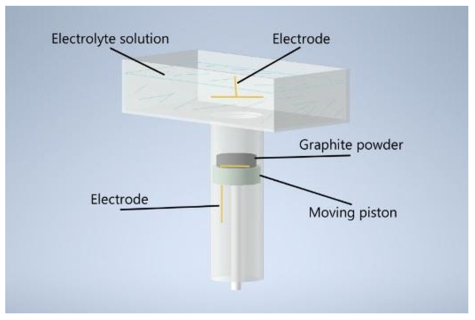
Figure 2.
AFM images of individual flakes: (a) MOG; (b) aMOG–200. The height profiles of the flakes are shown at the bottom.
Figure 2.
AFM images of individual flakes: (a) MOG; (b) aMOG–200. The height profiles of the flakes are shown at the bottom.
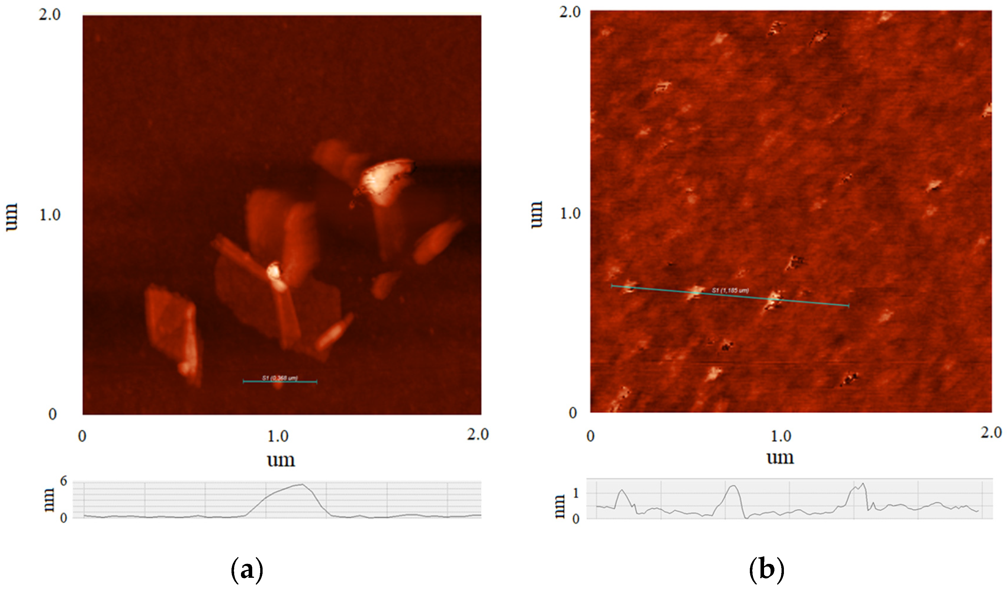
Figure 3.
SEM images: (a) MOG; (b) aMOG–200.
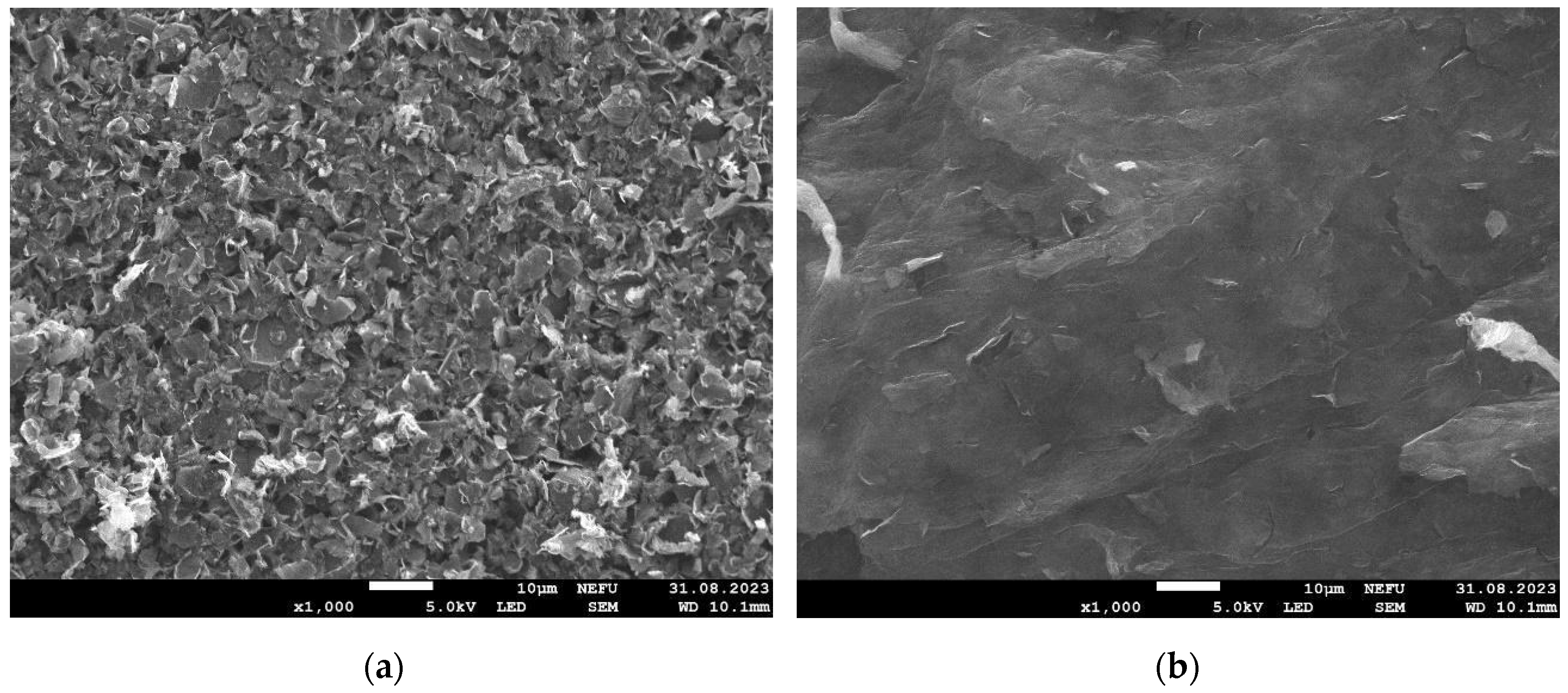
Figure 4.
(a) FTIR–spectra of MOG and aMOG–220; (b) Raman spectra of the MOG and aMOG–220.
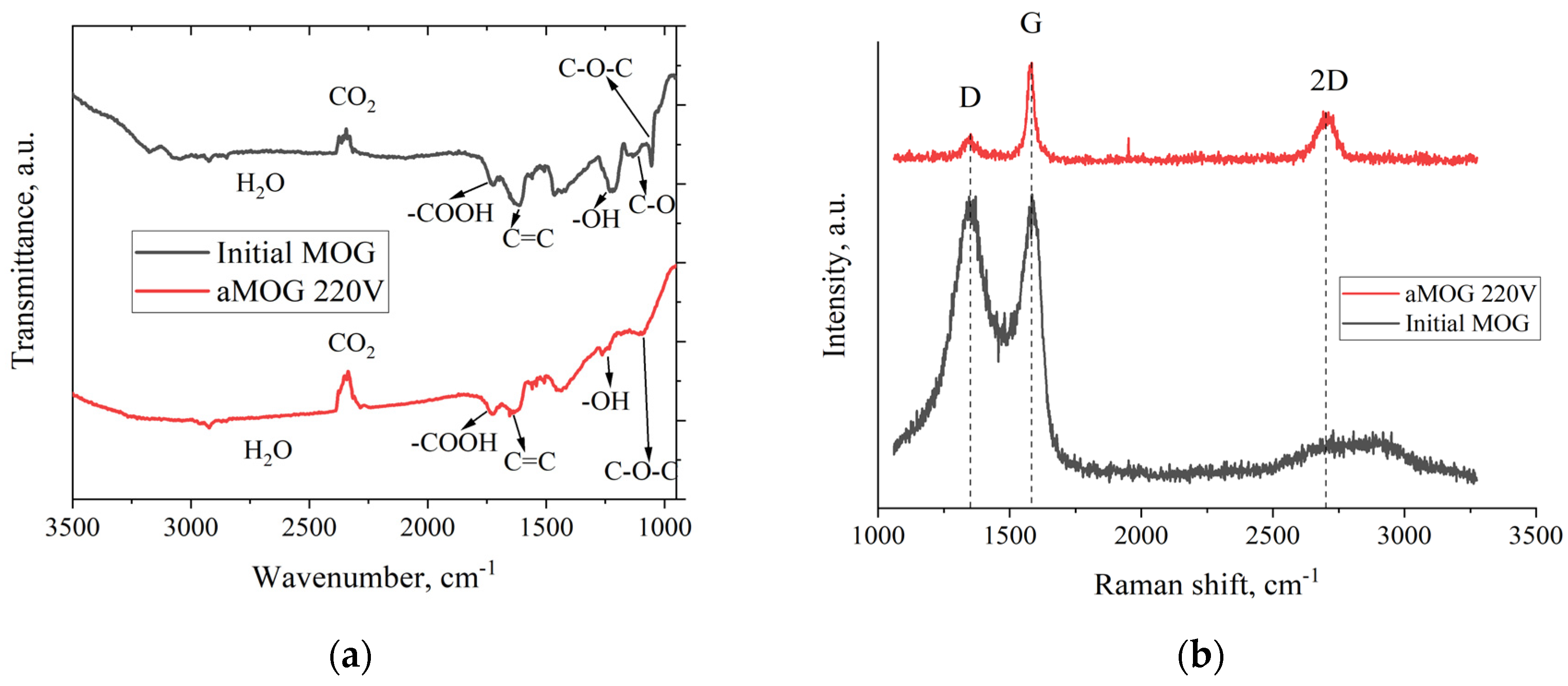
Figure 5.
(a) Raman spectra of samples obtained after fast joule heating of the MOG at different voltages; (b) Lorentzians of the aMOG–220 Raman spectra.
Figure 5.
(a) Raman spectra of samples obtained after fast joule heating of the MOG at different voltages; (b) Lorentzians of the aMOG–220 Raman spectra.
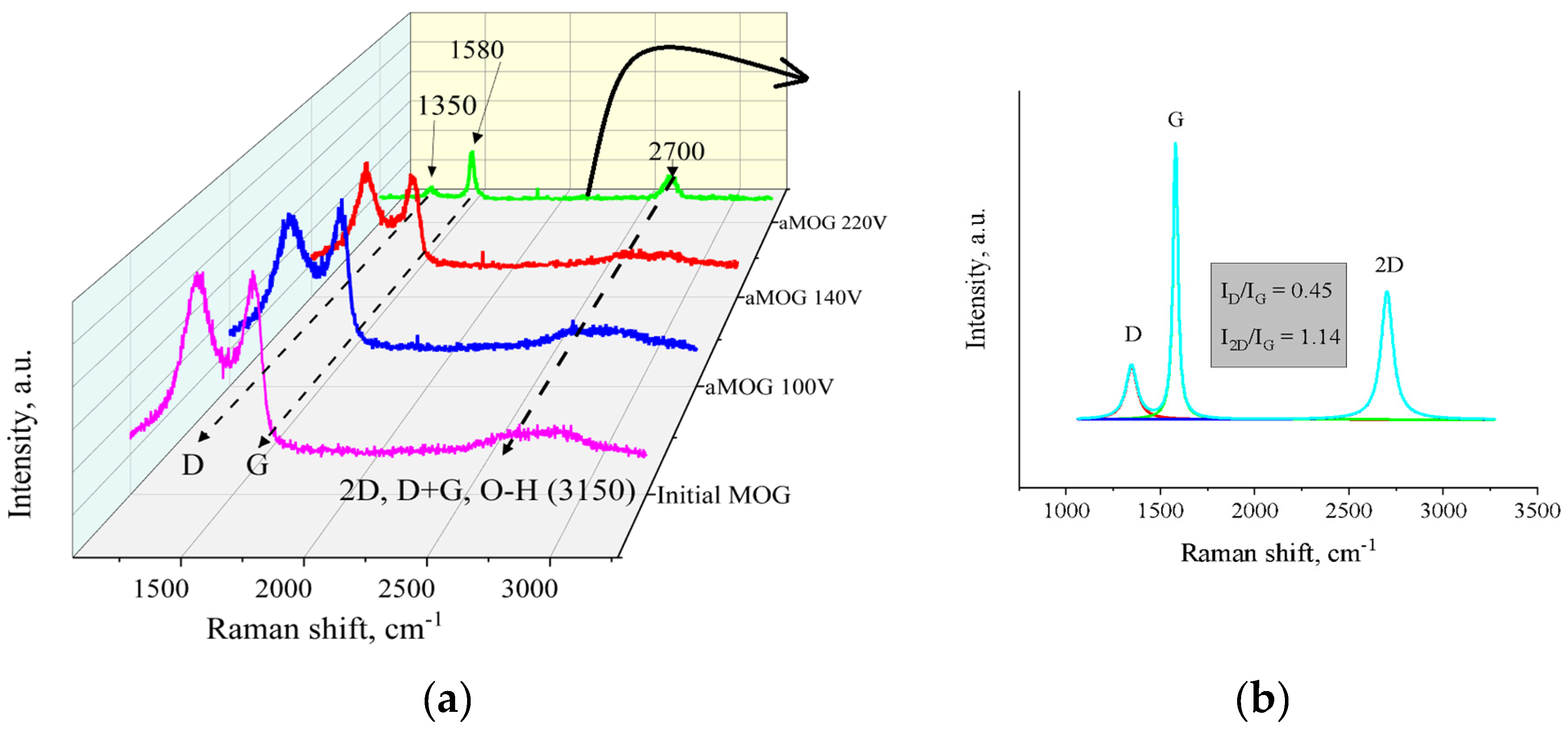
Figure 6.
Histogram of R/sq. and La distributions depending on treatment voltage.
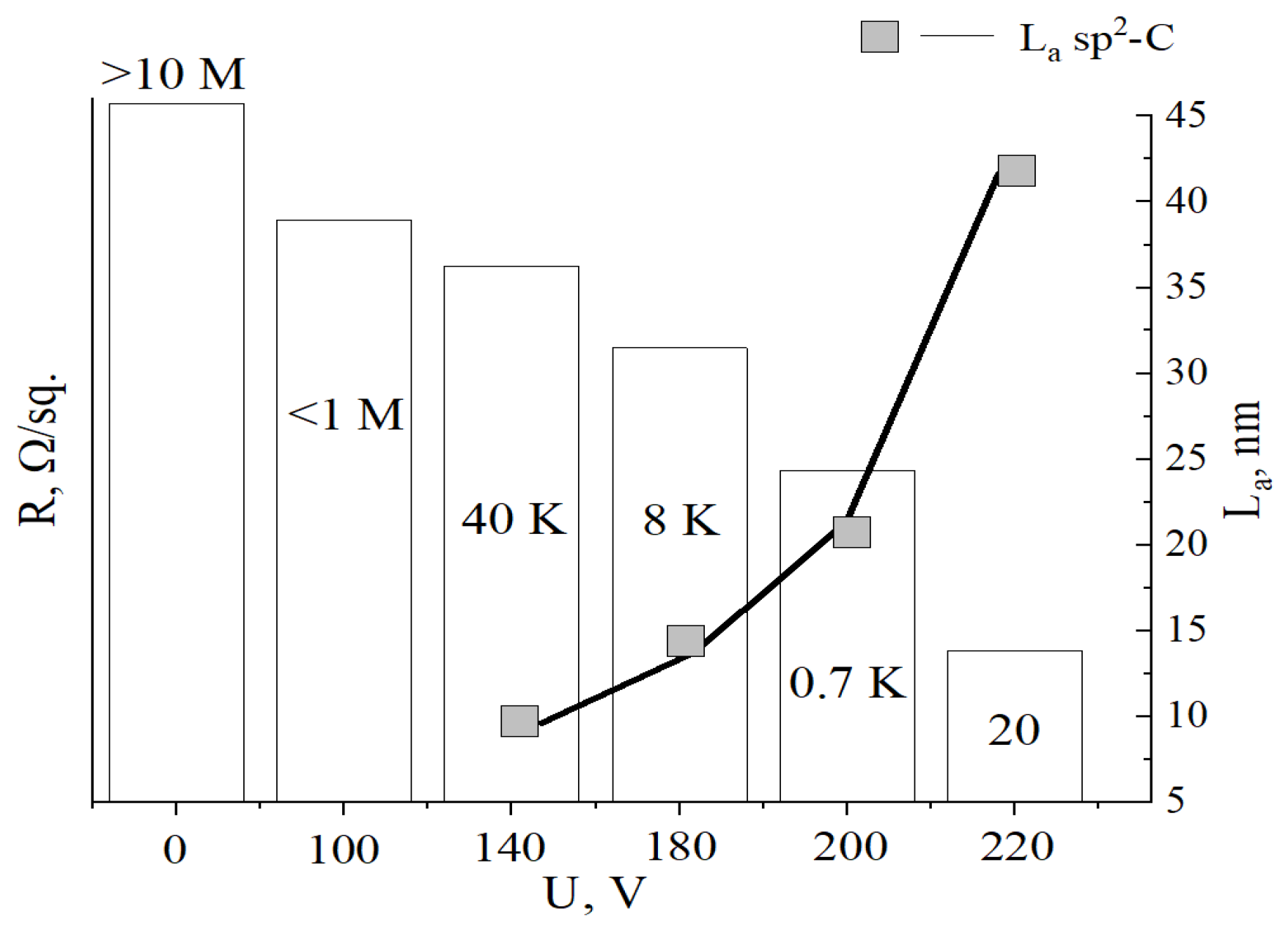
Figure 7.
(a) Typical isotherm of nitrogen adsorption–desorption on aMOG samples; (b) Distribution of the pore surface area of aMOG–200.
Figure 7.
(a) Typical isotherm of nitrogen adsorption–desorption on aMOG samples; (b) Distribution of the pore surface area of aMOG–200.
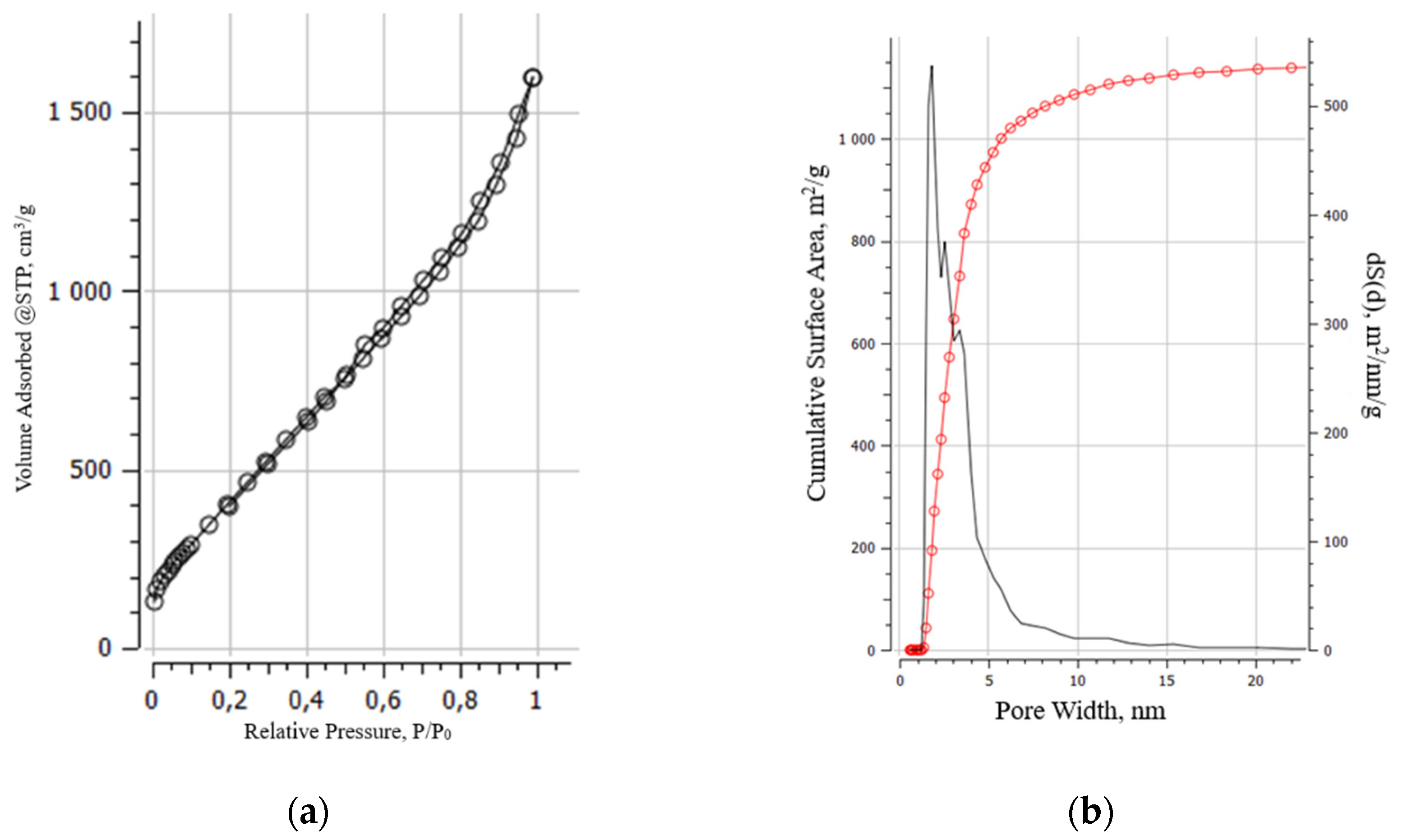

Table 1.
Carbon and oxygen content in MOG and aMOG–200 determined by EDS.
| Content | MOG | aMOG–200 |
|---|---|---|
| C, at. % | 85.9 | 95.8 |
| O, at. % | 14.1 | 4.2 |
Table 2.
Values of the surface resistance (R/sq.), ratio of Raman ID/IG peaks, and lateral sizes of sp2 crystallites (La), depending on the activation voltage.
Table 2.
Values of the surface resistance (R/sq.), ratio of Raman ID/IG peaks, and lateral sizes of sp2 crystallites (La), depending on the activation voltage.
| Voltage, V | Resistance, R/sq | ID/IG | La , nm |
|---|---|---|---|
| Initial MOG | >10 MΩ | >3 | – |
| 100 | <1 MΩ | >3 | – |
| 140 | 40 kΩ | <2 | 9.6 |
| 180 | 8 kΩ | 1.4 | 13.7 |
| 200 | 0.7 kΩ | 0.9 | 21.3 |
| 220 | 20 Ω | 0.45 | 42.6 |
Table 3.
Dependence of specific surface area on discharge voltage
| Voltage, V | SBET, m2/g |
|---|---|
| Initial MOG | 181.5 |
| 100 | 278.2 |
| 140 | 313.3 |
| 180 | 414.6 |
| 200 | 1984.5 |
| 220 | 260.5 |
Disclaimer/Publisher’s Note: The statements, opinions and data contained in all publications are solely those of the individual author(s) and contributor(s) and not of MDPI and/or the editor(s). MDPI and/or the editor(s) disclaim responsibility for any injury to people or property resulting from any ideas, methods, instructions or products referred to in the content. |
© 2024 by the authors. Licensee MDPI, Basel, Switzerland. This article is an open access article distributed under the terms and conditions of the Creative Commons Attribution (CC BY) license (http://creativecommons.org/licenses/by/4.0/).
Copyright: This open access article is published under a Creative Commons CC BY 4.0 license, which permit the free download, distribution, and reuse, provided that the author and preprint are cited in any reuse.


