Submitted:
17 January 2024
Posted:
18 January 2024
You are already at the latest version
Abstract
Changing the film thickness to manipulate the microstructural properties has been considered as a potential method in practical application. Here, we report that atomic-scale structural properties regulated by film thickness in NiCO2O4(NCO)/CuFe2O4(CFO) bilayer heterostructure prepared on (001)-MgAl2O4 (MAO) substrate by means of aberration-corrected scanning transmission electron microscopy (STEM). The misfit dislocations at NCO/CFO interface and antiphase boundaries (APBs) bound to dislocations within the films both are found in NCO (40 nm)/CFO (40 nm)/MAO heterostructure to contribute to relaxation of mismatch lattice strain. In addition, the non-overlapping a/4[101]-APB is found and the structural transformation of this kind of APB is resolved at atomic scale. In contrast, only the interfacial dislocations form at interface without the formation of APBs within the films in NCO (10 nm)/CFO (40 nm)/MAO heterostructure. Our results provide evidence that formation of microstructural defects can be regulated by changing film thickness to tune magnetic properties of epitaxial bilayer spinel oxide films.
Keywords:
bilayer heterostructure
; film thickness
; microstructural defects
; electron microscopy
1. Introduction
Spinel AB2O4 is widely used in microwave devices, spin filter devices and gas sensors due to its superior properties of high saturation magnetization, high spin polarizability, high resistivity, high permeability and low loss at high frequencies [1,2,3,4]. Among spinel ferrite, CFO has received much attention due to its unique structural and physical properties. It is believed that the Cu2+ ions tend to occupy octahedral (B-sites) sites, and the Fe3+ ions occupy both octahedral (B-sites) and (A-sites) tetrahedral sites. The bulk CFO with the cubic phase has a lattice parameter of 0.821 nm. In preparation of CFO thin films, the film-growth conditions have been found to affect cation distribution and phase stability of CFO films, which have a profound impact on the magnetic, electrical and optical properties of the films [5,6]. Another thin film layer of the bilayer heterojunction system is NCO, which is an inverse spinel structure, i.e., half of the Co3+ ions occupy in tetrahedra and the remaining Co3+ and Ni2+ ions occupy in octahedra, with a cubic phase structure and lattice constant of 0.811 nm. It is well-known that both electrical and magnetic properties are closely related to the film growth conditions in film systems [7,8,9]. The substrate temperature, film thickness and oxygen pressure are the important factors to tune the valence of anions and the respective occupancy in the polyhedral, further manipulating the strength of exchange interactions and ferromagnetic order, which in turn affects the general physical properties in NCO film system [10,11,12].
The NCO and CFO films grown on MAO (001) substrate form a bilayer subferromagnetic heterojunction, further generating exchange bias effect, which plays a crucial role in spintronics devices [13], also occurring in spinel oxide system [14,15,16]. The factors affecting the exchange bias effect are the respective structural characteristics and magnetic properties of the bilayer films, as well as the microstructure of the interface [17,18,19]. Particularly, the antiferromagnetic APBs bound to the interfacial dislocations normally form in the spinel film, in which the density and distribution of APBs would effectively affect the general magnetic properties [20,21]. It is very critical to manipulate the formation of planar defects APBs in a controllable and reliable manner for the novel device applications [22,23,24]. Previous studies on the exchange bias effect have mostly focused on alloy and perovskite heterojunctions [25,26,27,28,29]. However, the microstructural properties related to exchange bias effect in bilayer spinel oxide heterojunctions has been rarely reported. Here, we focus on atomic-scale structural properties of bilayer heterosystem consisting of both spinel film regulated by film thickness.
In present work, atomic-scale structural properties at interfaces and within the films in NCO/CFO bilayer heterostructure with different top film thickness were investigated by means of aberration-corrected scanning transmission electron microscopy. The structural transform of APB is determined by atomic-resolution high angle annular dark field (HAADF) imaging. Misfit strain relaxation in the bilayer heterostructure has been characterized. In particular, our results demonstrate that atomic-scale structural properties and formation of APBs can be regulated by film thickness in spinel bilayer heterostructure.
2. Materials and Methods
The CFO thin films were fabricated on single-crystal MAO (001) substrates by magnetron sputtering deposition. After that, the NCO thin film was deposited on CFO thin film forming the bilayer heterostructures. The MAO (001) substrates with one side polished (surface roughness:<0.5 nm) were purchased from MTI Corporation. Base pressure of deposition chamber was 10−5 Pa and the target-substrate distance was 15 cm. The growth of the bottom CFO films and top NCO films were at substrate temperature 400 °C and under the pressure of 50 Pa and 75 Pa with a mixed atmosphere of Ar2 (99.99%) and O2 (99.99%) in the ratio of 1:1. The power density on the target was 5.1 W/cm2. Two samples with different film thickness were investigated in this paper. One sample is NCO (40 nm)/CFO (40 nm)/MAO (001), and another sample is NCO (10 nm)/CFO (40 nm) /MAO (001).
Two (S)TEM specimens were prepared by focused ion beam (FIB) lift-out technique using an FEI Helios600i FIB/SEM system. FIB lamellae were cut along the <110> orientations of the MAO substrate. TEM images were carried out on an FEI Titan 80-300 microscope equipped with an aberration corrector for objective lens, operated at 300 kV. HAADF imaging was performed on a JEOL-ARM200F with a probe aberration corrector, operated at 200 kV. In STEM mode, a probe size of 0.1 nm at semi-convergence angle of α=22 mrad was used for HAADF imaging experiments. The HAADF detectors covered angular ranges of 90~176 mrad.
3. Results and discussions
Figure 1(a) displays a low-magnification BF-TEM image, showing the cross-sectional overview of the NCO (40 nm)/CFO (40 nm) film on the MAO (001) substrate, viewed along the [10] zone axis of MAO. From the cross-sectional image, the thicknesses of NCO/CFO film are measured to be both about 40 nm. The film interfaces were distinguished to be visible according to contrast variation within the film, as indicated by two horizontal white arrows. Figure 1(b) shows a typical SAED pattern of the NCO/CFO film and part of the MAO substrate, recorded along the [10] zone axis of MAO substrate. The splitting of the 026 and 004 reflections along out-of-plane directions is discerned, indicating that the mismatch strain between film and substrate relaxes along out-of-plane. In contrast, the splitting of 440 diffraction reflection along in plane is not observed, as shown by the magnified part in the insert in Figure 1(b). Particularly, the reflection spot splitting between bilayer films is neither observed along in-plane and out-of-plane. Figure 1(c–e) are EDS mapping images acquired from the regions marked by the white square in (a), representing the signals of Co−Kα1, Fe−Kα1, Al−Kα1, respectively. The EDS results imply the truth that NCO film is fabricated on the top of the CFO film. From the result of SAED, it seems that the relaxation of epitaxial mismatch strain between two films along in-plane does not occur. The further investigation needs to be performed to distinguish the microstructures within the bilayer films and across the interfaces.
The bilayer heterostructure of NCO (40 nm)/CFO (40 nm)/MAO is further examined by atomic resolution HAADF imaging as shown in Figure 2, viewed along [10] zone axis of MAO. Based on the principle of Z contrast in HAADF imaging and element atom number (ZNi=28, ZCo=27, ZCu=29, ZFe=26), the brighter spots in HAADF image are caused by the higher atom column density that is two times that of the darker spots along [10] zone axis [30]. The HAADF images in Figure 2(a, b) contains the interface between CFO film and MAO substrate and NCO film and CFO film, respectively, which shows the epitaxial interfaces at part of regions and no interfacial dislocations form at this region.
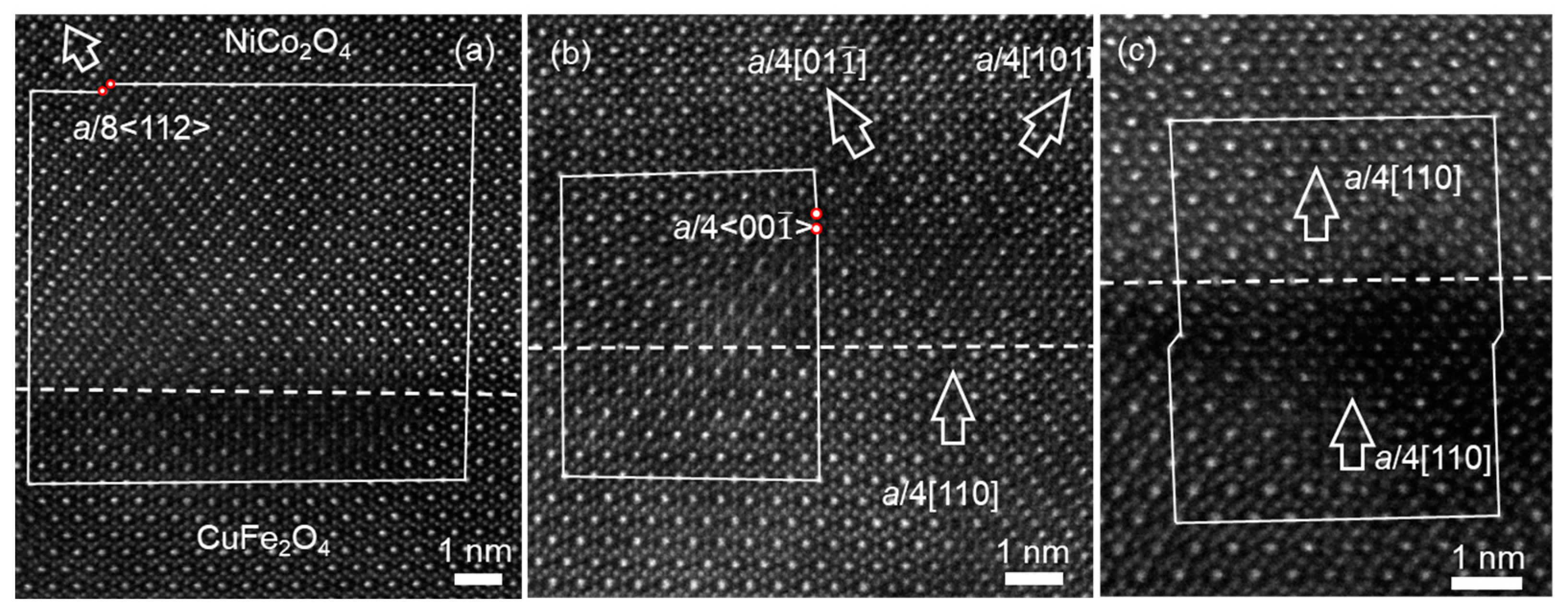
As a contrast, the high resolution HAADF images were acquired from other regions across the interface between NCO film and CFO film, viewed along [10] zone axis of MAO substrate, as shown in Figure 3. The interface between NCO film and CFO film were denoted by the horizontal white dashed line. Remarkably, the interfacial dislocations and planar defects were both observed. The image in Figure 3(a) contains an interfacial dislocation with the projected displacement of an/8<112> (an is lattice parameter of NCO film), acquired by the Burger circuit. This dislocation then induces an APB propagating into the NCO film as indicated by the oblique white arrow. The APB is located at (11) plane and composed of octahedral B-site cations of the two domain regions separated by the APB. Neither overlapping of the two domains nor blurred area across the APB was observed. For clarity, this kind of APB is called a non-overlapping APB-I.
Figure 3(b) suggests that an ac/4[110]-APB, which is edge-on along [10] viewing direction, marked by the white vertical arrow, forms within CFO film nearby the interface. The APB penetrated across the interface between NCO film and CFO film, propagated into the NCO film and decomposed into two APBs with the displacement vector of an/4[01] and an/4[101], marked by two oblique white arrows, respectively. These two APBs have the projected displacement vector an/8<112> along [10] direction. The regions across two APBs are blurred, both of which are the overlapping regions of the two domains, which was also observed in our previous work [31]. In addition, a dislocation with the projected displacement vector of an/4<00> exists at the interface acquired by the Burger circuit. The dislocation core lies within NCO film, which is connected with the APB of an/4[01] in NCO film. Eventually, the dislocation terminates at this APB.
Figure 3(c) shows that an edge-on APB with the displacement of ac/4[110] forms within the CFO film nearby the interface, as marked by the lower white arrow, which crosses the interface, penetrated into the NCO film and translates along the [0] crystal direction, as marked by the upper white arrow. It is noticeable that there is no formation of interfacial dislocation in this region by the closed Burger circuit containing the interface and two APBs.
In NCO (40 nm)/CFO (40 nm) heterostructure, interfacial dislocations and the APBs within the film form to relax the epitaxial mismatch strain between NCO and CFO film. The heterostructure interface can both terminate the APBs formed in the CFO film and become the start point of the APB formation in the NCO film.
Figure 3.
(a–c) Atomic-resolution HAADF images of the heterostructure interfaces between NCO film and CFO film in different regions denoted by white dashed lines, showing the interfacial dislocations with different Burgers vectors. The oblique arrows marked the APBs in films.
Figure 3.
(a–c) Atomic-resolution HAADF images of the heterostructure interfaces between NCO film and CFO film in different regions denoted by white dashed lines, showing the interfacial dislocations with different Burgers vectors. The oblique arrows marked the APBs in films.
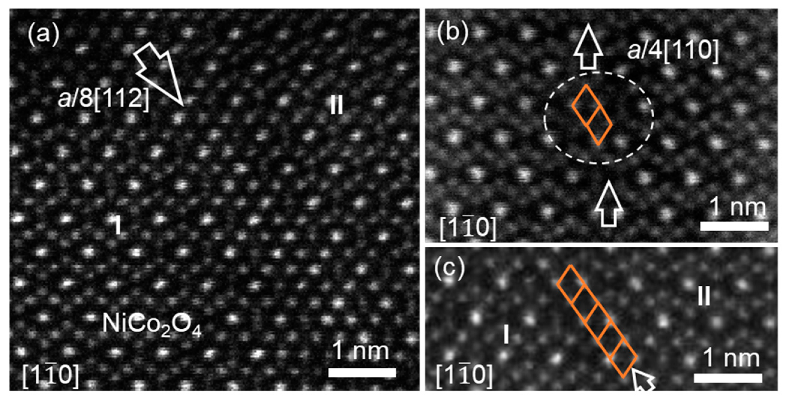
In addition, the structural transformation of non-overlapping APB is observed and resolved for the first time in the NCO films, which are shown in the HAADF images of Figure 4(a–c), recorded along the [10] zone axis of the film. In Figure 4(a), the white oblique arrow denotes the non-overlapping APB-I with the projected displacement of an/8[112], which separated the film into domain I and domain II. It can be seen that the APB lies in (11) plane and consists of B-site cations of both domain I and II. It should be noted that the present APB does not appear overlapped regions, but present the sharp boundary. In fact, the full displacement vector of this type of APB can be deduced to be an/4[101] = an/8[112] + an/8[10] (or an/4[011] = an/8[112] + an/8[10]) taking account of the displacement along [10] zone axis, which suggests that the domains separated by this kind of APB is also displaced by 1/8 atomic plane in the [10] viewing direction, eventually forming the non-overlapping APB-I. Particularly, this type of APB was also observed in CFO film.
Figure 4(b) shows the atomic resolution HAADF image containing the translation of edge-on APBs. The two edge-on APBs both have the displacement vector of an/4[110], recorded along [10] zone axis. The an/4[110]-APB denoted by lower vertical arrow is displaced along [112] crystal orientation and formed the other an/4[110]-APB denoted by upper vertical arrow. The area circled by the oval dotted box is the connection point at the two APBs before and after the translation, as shown by two connected brown diamonds in the Figure 4(b) (the four vertices of brown diamond are the locations of octahedral B-site cations). Remarkably, Figure 4(c) shows the continuous translation of an/4[110]-APB along [112] crystal orientation, denoted by a series of brown diamonds, which generates the domain boundary. And it is called as non-overlapping APB-II for clarity, marked by the oblique white arrow. The non-overlapping APB-II also lies in (11) plane and separates the film into domain I and domain II, and the boundary consists of the octahedral B-site cations of both domain I and II. However, it is different from the non-overlapping APB-I in Figure 4(a). It appears that the non-overlapping APB-I in Figure 4(a) shifted by 1/8 atomic plane along [112] crystal orientation would form non-overlapping APB-II in Figure 4(c). For more clear explanation, the further investigation can be performed using structure models established by Vesta [32].
Figure 4.
(a–c) Atomic-resolution HAADF images of NCO film in different regions, showing the non-overlapping APB located in (11) plane. The white arrows marked the APBs in films. The orange lozenges represent the shift of the APB.
Figure 4.
(a–c) Atomic-resolution HAADF images of NCO film in different regions, showing the non-overlapping APB located in (11) plane. The white arrows marked the APBs in films. The orange lozenges represent the shift of the APB.
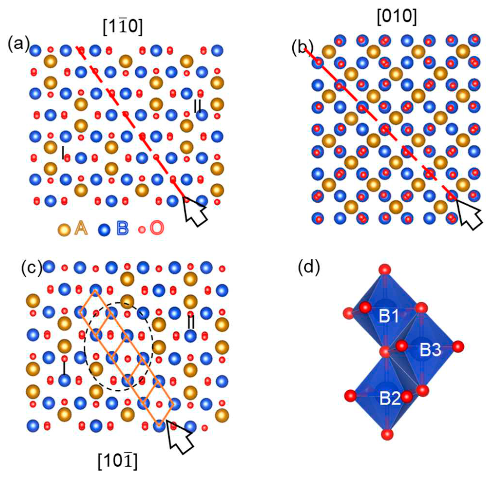
On the basis of results in Figure 4 and shift vector of a/4[101] = a/8[112] + a/8[10], the atomic details of translation and transformation of non-overlapping APB can be understood by establishing the structural models along [10], [010] and [101] directions as shown in Figure 5. In the APBs structural models, the tetrahedral sites (A-sites) in AB2O4 are highlighted in orange, and octahedral sites (B-site) highlighted in blue. Figure 5(a) shows the structural model of the non-overlapping APB-I with the displacement of a/4[101] projected along the [10] viewing direction. It can be seen that the oxygen sublattice in perfect lattice is maintained across such non-overlapping APB-I, while the regular cation arrangement is interrupted. The non-overlapping APB-I is denoted by a red dashed line and lies in (11) plane, which consists of only B-site cations of two separated domain I and II. Then, rotating and seeing the structural model in [010] viewing direction, as shown in structural model of Figure 5(b), the APB is marked by the red dashed line, while the displacement induced by this APB does not induce a visible difference across the APB in this viewing direction, as a result, the disturbance of the cation sublattice at the APB cannot be recognized. Continuously rotating the structural mode of in Figure 5(a) and viewing it in [10] direction, as shown in Figure 5(c), it is obvious that the atomic structural model in Figure 5(c) is the same as the atomic arrangement in Figure 4(c). The formation of structural model in Figure 5(c) can be understood by the continuous translation of edge-on a/4[101]-APB along [121] crystal orientation, as shown in the brown diamonds and the connection point at the two APBs before and after the translation was also circled by the oval dotted box, which is consistent with the HAADF result in Figure 4(b). The edge-on a/4[101]-APB continuously translating along the [121] crystal orientation would result in the formation of non-overlap APB-II. Consequently, the non-overlapping APB-I with the displacement of a/4[101] in the [10] viewing orientation can be formed by edge-on a/4[101]-APB in the [10] viewing orientation continuously translating along the [121] crystal orientation, eventually making non-overlapping APB-I lies in (11) habit plane. Obviously, the non-overlapping APB-I in Figure 5(a) projected in [10] shifted by 1/8 atomic plane along [112] crystal orientation would form the non-overlapping APB-II in Figure 5(c) projected in [10], which is consistent with the results of HAADF experiment in Figure 4.
To further clarify the atomic arrangement at the non-overlapping APB observed in the film, the schematic model of this kind of APB is displayed in Figure 5(d). In contrast to edge-sharing octahedra in perfect AB2O4 lattice, across the non-overlapping APB, both edge-sharing and corner-sharing octahedra coexist. For clear, the octahedra at the APB are marked as B1, B2 and B3, in fact, the cations located at these octahedra have the same coordination environment of oxygen octahedron. It can be seen that octahedra B1 and B3 (B2 and B3) share edge with bond angle of 90 degrees, and octahedra B1 and B2 share corner with bond angle of 180 degrees. As a result, a strong antiferromagnetic superexchange interaction occurs across the non-overlapping APB [21], which is speculated to be an antiferromagnetic interface.
Figure 5.
(a, c) The structure models of APB, viewed along the [10] MAO zone axis. (b) The structure models of APB, viewed along the [010] MAO zone axis. The APB plane is marked by red dashed line, respectively. (d) the structure model showing the corner-shared octahedral cations at APB.
Figure 5.
(a, c) The structure models of APB, viewed along the [10] MAO zone axis. (b) The structure models of APB, viewed along the [010] MAO zone axis. The APB plane is marked by red dashed line, respectively. (d) the structure model showing the corner-shared octahedral cations at APB.
In order to understand the formation of dislocations and planar defects in different film thickness of NCO/CFO/MAO bilayer heterostructures, the NCO (10 nm)/CFO (40 nm) bilayer films were prepared on the MAO (001) substrate under the same deposition condition. The thickness of the NCO film changes, the heterojunction interface between the two films and the microstructures inside the film will change.
The cross-sectional overview of the NCO (10 nm)/CFO (40 nm) film prepared on the MAO (001) substrate, viewed along the [10] zone axis of MAO was shown in Figure 6(a). The film interface was also visible according to contrast variation within the film, as indicated by two horizontal white arrows. Figure 6(b) shows a typical SAED pattern of the NCO/CFO film and part of the MAO substrate, recorded along the [10] zone axis of MAO substrate. The splitting of the 026 and 004 reflections along out-of-plane directions is discerned, while the splitting of 440 diffraction reflection along in-plane is not observed. Particularly, the reflection splitting of bilayer films is neither observed along in-plane and out -of-plane. High resolution HAADF imaging was further conducted at the interface of bilayer film. Figure 6(c) displays the smooth epitaxial interfaces, marked by the horizonal white line, without the formation of interfacial dislocations at this region. In contrast, the interfacial dislocations with different burgers vector were found at the interface in other interfacial regions.
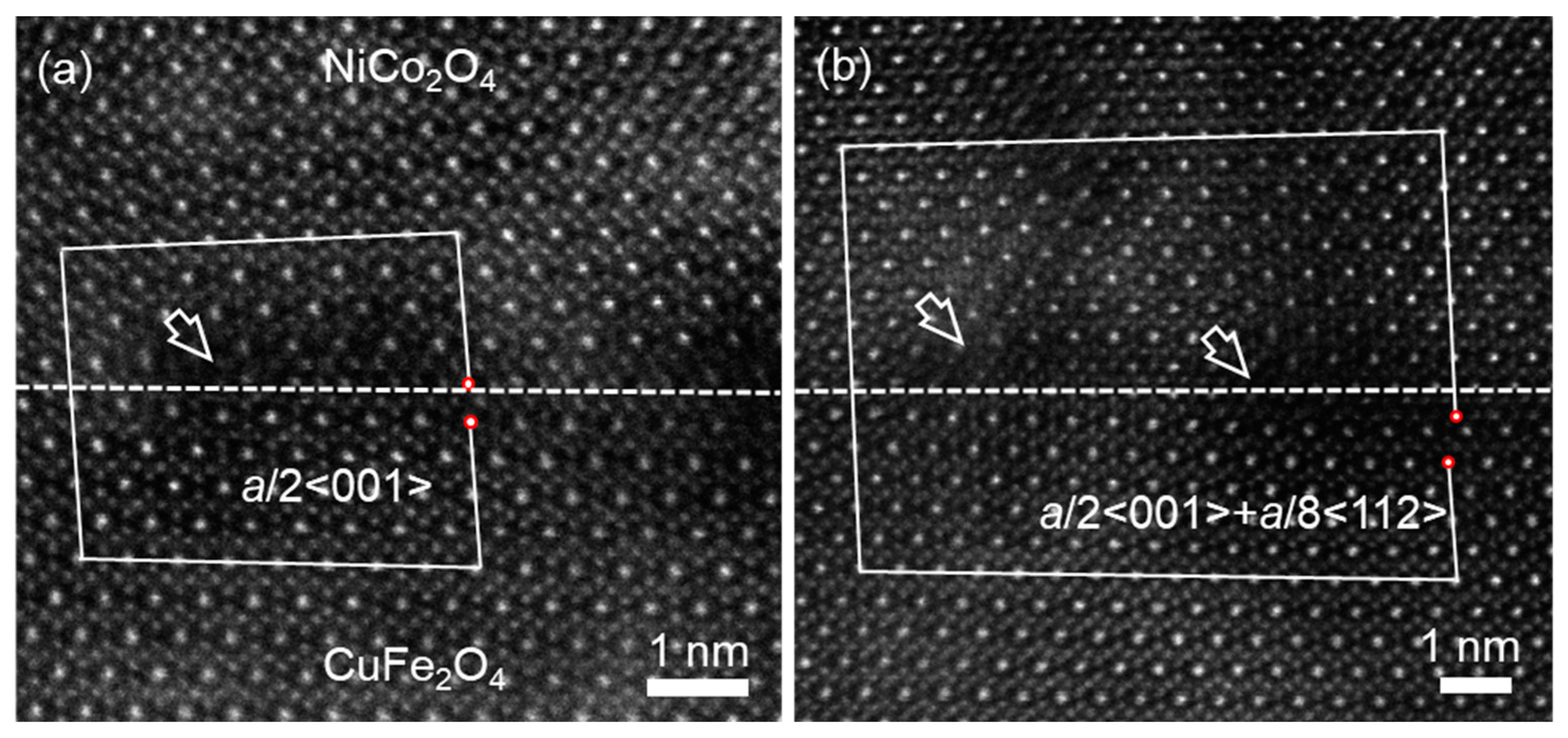
Figure 7(a) displays an atomic-resolution HAADF image of the NCO (10 nm)/CFO (40 nm) interface, recorded along the [10] zone axis of the MAO substrate, showing the existence of interfacial dislocations. Performing a Burger circuit around the isolated misfit dislocation core leads to a projected displacement vector of ac/2<001>. It is obvious that dislocation core, marked by the white arrow, is located inside the NCO film near the interface. In addition, another kind of interfacial dislocation with the projected displacement vector of ac/2<001>+ac/8<112> was observed at interface shown in Figure 7(b), acquired by the Burger circuit containing two dislocation cores, one core located inside the NCO film adjacent to the interface and another core located at the interface, as indicated by two white arrows in Figure 7(b). It should be noted that these two dislocations neither does not further lead to the formation of APBs in two films, which is different from that in NCO (40 nm)/CFO (40 nm)/MAO heterostructure. The formation of interfacial dislocation contributes to relaxation of epitaxial mismatch strain between NCO and CFO film.
Two NCO/CFO/MAO heterosystems with different film thickness were prepared under the same deposition condition. Different microstructural defects are generated inside and at the interface of the two films due to the different thickness of the upper film NCO.
In NCO/CFO bilayer heterostructure, the in-plane lattice mismatch between NCO and CFO materials is calculated to be −2.59% by using (aN−aC)/aC*100%, where aN and aC are the parameters of bulk NCO and CFO materials, respectively. The formation of both interfacial dislocations and APBs within the film in the NCO (40 nm)/CFO (40 nm) heterostructure contribute to epitaxial strain relaxation from lattice mismatch more effectively than that in NCO (10 nm)/CFO (40 nm) heterostructure. In some case, the misfit dislocations are nucleation sites of the APBs in the NCO (40 nm)/CFO (40 nm) heterostructure. This means that the density of the APBs in the film depends on the density of the misfit dislocations. It is well known that the strain state in the heterosystem can be affected by the thickness of the films [33], as a result, the density of the misfit dislocations and the formation of APBs changes with the film thickness, which is demonstrated that the density of interfacial dislocation in the NCO (40 nm)/CFO (40 nm) heterosystem is greater than that in the NCO (10 nm)/CFO (40 nm) heterosystem and APBs form in the NCO (40 nm)/CFO (40 nm) rather than NCO (10 nm)/CFO (40 nm) heterosystem. Moreover, the edge-on APBs and non-overlapping APBs in the NCO (40 nm)/CFO (40 nm) heterostructure both exhibit antiferromagnetic coupling, which would affect the ferromagnetic properties of the films. Accordingly, atomic-scale structural properties including the formation of APBs in the heterostructure could be tuned by the film thickness, which may allow further manipulating the magnetic properties of films.
4. Conclusions
The microstructural properties in NCO/CFO/MAO bilayer heterostructure regulated by the film thickness have been characterized at the atomic scale using aberration-corrected STEM. The interfacial dislocations of different Burger vectors form at the interface and antiferromagnetic APBs bound to the dislocations are generated inside the film in the NCO (40 nm)/CFO (40 nm) heterostructure. The non-overlapping APBs were found and the structural transform of non-overlapping APBs was resolved at atomic scale. In contrast, in the NCO (10 nm)/CFO (40 nm) heterosystem, only interfacial dislocations of different Burger vectors form at the NCO/CFO interface, which does not further cause the formation of APBs in films. The formation of interfacial dislocations and APBs in NCO (40 nm)/CFO (40 nm) heterostructure contribute to the relaxation of mismatch strain more effectively. Therefore, our results demonstrate that changing the thickness of the top layer of the bilayer heterostructure can manipulate the microstructure at the interface and the formation of APB inside the film and further influence the physical properties (e.g., exchange bias effects and magnetoresistance).
Author Contributions
Conceptualization, K.L.; investigation, K.L.; writing—original draft preparation, K.L.; writing—review and editing, K.L., J.L., and S.Z.; supervision, J.L. All authors have read and agreed to the published version of the manuscript. All authors have read and agreed to the published version of the manuscript.
Funding
This research was funded by the Natural Science Foundation of the Jiangsu Higher Education Institutions of China (Grant: 23KJB510032 & 21KJB510022), the Science and Technology Planning Project of Suzhou City (No. SZS2022015) and Cultivation project of Suzhou vocational University (SVU2021py02).
Data Availability Statement
Data are contained within the article and supplementary materials.
Acknowledgments
We thank the Suzhou Key Laboratory of Smart Energy Technology for their support with the experiments of characterization.
Conflicts of Interest
The authors declare no conflicts of interest.
References
- Suzuki, Y.; VanDover, R.B.; Gyorgy, E.M.; Phillips, J.M.; Korenivski, V.; Werder, D.J.; Chen, C.H.; Cava, R.J.; Krajewski, J.J.; Peck, W.F.; Do, K.B. Structure and Magnetic Properties of Epitaxial Spinel Ferrite Thin Films. Appl. Phys. Lett. 1996, 68, 714–716. [Google Scholar] [CrossRef]
- Hcini, S.; Brahmi, M.; Dhaou, M.H.; Khirouni, K.; Mallah, A.; Mashary, F.S.A.; Albadri, A.E. Studies of Structural, Dielectric, and Optical Properties of CuCoFeO4 Spinel for High Frequency, Microwave, and Optoelectronic Applications. J. Mol. Struct. 2023, 1291, 135981. [Google Scholar] [CrossRef]
- Zhang, R.; Qin, C.; Bala, H.; Wang, Y.; Cao, J. Recent Progress in Spinel Ferrite (MFe2O4) Chemiresistive Based Gas Sensors. Nanomaterials 2023, 13, 2188. [Google Scholar] [CrossRef] [PubMed]
- Anandan, S.; Selvamani, T.; Prasad, G.G.; Asiri, A.M.; Wu, J.J. Magnetic and Catalytic Properties of Inverse Spinel CuFe2O4 Nanoparticles. J. Magn. Magn. Mater. 2017, 432, 437–443. [Google Scholar] [CrossRef]
- Yang, A.; Chen, Z.; Islam, S.M.; Vittoria, C.; Harris, V.G. Cation Engineering of Cu-ferrite Films Deposited by Alternating Target Laser Ablation Deposition. J. Appl. Phys. 2008, 103, 07E509. [Google Scholar] [CrossRef]
- Ati, A.A.; Abdalsalam, A.H.; Abbas, H.H. Influence of Annealing on Structural, Morphology, Magnetic and Optical Properties of PLD Deposited CuFe2O4 Thin Films. Inorg. Chem. Commun. 2022, 146, 110072. [Google Scholar] [CrossRef]
- Xu, X.S.; Mellinger, C.; Cheng, Z.G.; Chen, X.G.; Hong, X. Epitaxial NiCo2O4 Film as an Emergent Spintronic Material: Magnetism and Transport Properties. J. Appl. Phys. 2022, 132, 020901. [Google Scholar] [CrossRef]
- Liu, L.; Zhen, C.M.; Xu, L.; Shui, Z.Z.; Ma, L.; Zhao, D.W.; Hou, D.L. Semiconductor-Metal Transition in Vulcanized NiCo2O4 Film. J Phys. Chem. Solids 2023, 174, 111189. [Google Scholar] [CrossRef]
- Zhen, C.M.; Zhang, X.Z.; Wei, W.G.; Guo, W.Z.; Pant, A.; Xu, X.S.; Shen, J.; Ma, L.; Hou, D.L. Nanostructural Origin of Semiconductivity and Large Magnetoresistance in Epitaxial NiCo2O4/Al2O3 Thin Films. J. Phys. D 2018, 51, 145308. [Google Scholar] [CrossRef]
- Bitla, Y.; Chin, Y.Y.; Lin, J.C.; Van, C.N.; Liu, R.R.; Zhu, Y.M.; Liu, H.J.; Zhan, Q.; Lin, H.J.; Chen, C.T.; Chu, Y.H.; He, Q. Origin of Metallic Behavior in NiCo2O4 Ferrimagnet. Sci. Rep. 2015, 5, 15201. [Google Scholar] [CrossRef]
- Kim, J.; Park, Y.J.; Dho, J. Ferrimagnetic and Metallic Properties of (001) NiCo₂O₄ Films Fabricated at Various Oxygen Pressures. J. Magn. 2023, 28. [Google Scholar] [CrossRef]
- Wu, C.F.; Zhen, C.M.; Zhang, X.Z.; Xu, X.S.; Xie, J.T.; Ma, L.; Zhao, D.W.; Hou, D.L. Sensitive Metallic Behavior in Epitaxial NiCo2O4 Films Regulated by the Film Thickness. J Phys. Chem. Solids 2022, 160, 110321. [Google Scholar] [CrossRef]
- Lee, M. Disordered Exchange is Biased. Nat. Phys. 2021, 17, 434–435. [Google Scholar] [CrossRef]
- Hassnain Jaffari, G.; Bah, M.; Ismat Shah, S. Strong Magnetic Coupling Between Antiferromagnetic and Ferromagnetic Phases in Polycrystalline Hollow Nanoparticles Composed of Spinel Solid Solution. J. Alloys Compd. 2021, 857, 157607. [Google Scholar] [CrossRef]
- Muzzi, B.; Albino, M.; Petrecca, M.; Innocenti, C.; de Julián Fernández, C.; Bertoni, G.; Ibarra, M.R.; Christensen, M.; Avdeev, M.; Marquina, C.; Sangregorio, C. Defect-engineering by Solvent Mediated Mild Oxidation as a Tool to Induce Exchange Bias in Metal Doped Ferrites. Small Methods 2023, 7, 2300647. [Google Scholar] [CrossRef] [PubMed]
- Beatriz, R.M.; Martín, T.A.; Skorikov, A.S.; Miguel, C.H.; Bals, S.; Salgueiriño, V. Interfaceless Exchange Vias in CoFe2O4 Nanocrystals. Nano Letters 2023, 23, 1688–1695. [Google Scholar] [CrossRef]
- Díez, J.M.; Cuñado, J.L.F.; Lapa, P.; Solís, R.; Arnay, I.; Pedraz, P.; Perna, P.; Bollero, A.; Miranda, R.; Schuller, I.K.; Camarero, J. Interfacial Exchange Phenomena Driven by Ferromagnetic Domains. Adv. Mater. Interfaces 2022, 9, 2200331. [Google Scholar] [CrossRef]
- Kim, J.V.; Stamps, R.L. Defect-modified Exchange Bias. Appl. Phys. Lett. 2001, 79, 2785–2787. [Google Scholar] [CrossRef]
- Khan, A. The Effect of Antisite Disorder on Magnetic and Exchange Bias Properties of Gd-substituted Y2CoMnO6 Double Perovskite. J. Phys. Condens. Matter. 2022, 34, 435801. [Google Scholar] [CrossRef]
- McKenna, K.P.; Hofer, F.; Gilks, D.; Lazarov, V.K.; Chen, C.; Wang, Z.; Ikuhara, Y. Atomic-scale Structure and Properties of Highly Stable Antiphase Boundary Defects in Fe3O4. Nat. Commun. 2014, 5, 5740. [Google Scholar] [CrossRef]
- Li, Z.; Lu, J.; Jin, L.; Rusz, J.; Kocevski, V.; Yanagihara, H.; Kita, E.; Mayer, J.; Dunin-Borkowski, R.E.; Xiang, H.; Zhong, X. Atomic Structure and Electron Magnetic Circular Dichroism of Individual Rock Salt Structure Antiphase Boundaries in Spinel Ferrites. Adv. Funct. Mater. 2021, 31, 2008306. [Google Scholar] [CrossRef]
- Mi, S.B.; Zhang, R.Y.; Lu, L.; Liu, M.; Wang, H.; Jia, C.L. Atomic-scale Structure and Formation of Antiphase Boundaries in α-Li0.5Fe2.5O4 Thin Films on MgAl2O4(001) Substrates. Acta Mater 2017, 127, 178–184. [Google Scholar] [CrossRef]
- Ahmed, S.; Pokle, A.; Bianchini, M.; Schweidler, S.; Beyer, A.; Brezesinski, T.; Janek, J.; Volz, K. Understanding the Formation of Antiphase Boundaries in Layered Oxide Cathode Materials and Their Evolution Upon Electrochemical Cycling. Matter 2021, 4, 3953–3966. [Google Scholar] [CrossRef]
- Lee, D.W.; Trang, T.T.; Heo, Y.U. Role of Dislocation Climb on Twin Boundary and Antiphase Boundary Formations in Inverse-Spinel MnAl2O4. J. Alloys Compd. 2023, 958, 170526. [Google Scholar] [CrossRef]
- Cao, K.Y.; Tian, F.H.; Huang, S.; Zhang, Y.; Zhao, Q.Z.; Yao, K.K.; Dai, Z.Y.; Li, J.N.; Yu, Z.H.; Zhou, C.; Ke, X.Q.; Song, X.P.; Yang, S. Tuning the Exchange Bias Effect Via Thermal Treatment Temperature in Bulk Ni50Mn42In3Sb5 Heusler Alloys. Appl. Phys. Express 2021, 14, 105502. [Google Scholar] [CrossRef]
- Panigrahi, B.; Raja, M.M.; Murapaka, C.; et al. Bias-field-free Microwave Operation in NiFe/FeMn Exchange Biased Bilayers by Varying FeMn Thickness. J Supercond. Nov. Magn. 2023, 36, 1075–1083. [Google Scholar] [CrossRef]
- Sun, H.D.; Jing, C.; Su, Y.; Cai, F.Q.; Yang, S.Y.; Zhou, T.; Zhang, Y.L.; Li, Z. Spontaneous Exchange Bias and Magnetic Characteristics in Ni50Mn35Sn10V5 Heusler Alloy. Solid State Commun. 2023, 373–374, 115339. [Google Scholar] [CrossRef]
- Deng, Z.; Wang, X.; Wang, M.; et al. Giant Exchange-bias-like Effect at Low Cooling Fields Induced by Pinned Magnetic Domains in Y2NiIrO6 Double Perovskite. Adv. Mater. 2023, 35, 2209759. [Google Scholar] [CrossRef]
- Pal, K.; Das, I. The Impact of Oxygen Deficiency on Giant Exchange Bias in Perovskite Oxide: SrFe0.5Co0.5O3−δ (δ = 0.37). J. Alloys Compd. 2023, 960, 170794. [Google Scholar] [CrossRef]
- Pennycook, S.J.; Nellist, P.D. Z-contrast Scanning Transmission Electron Microscopy. In Impact of Electron and Scanning Probe Microscopy on Materials Research; 1999; pp. 161–207. [Google Scholar] [CrossRef]
- Liu, K.; Zhang, R.Y.; Lu, L.; Mi, S.B.; Liu, M.; Wang, H.; Jia, C.L. Formation of Antiphase Boundaries in CuFe2O4 Films Induced by Rough MgAl2O4 (001) Substrates. Thin Solid Films 2019, 680, 55–59. [Google Scholar] [CrossRef]
- Momma, K.; Izumi, F. VESTA 3 for three-dimensional visualization of crystal, volumetric and morphology data. J. Appl. Crystallogr. 2011, 44, 1272–1276. [Google Scholar] [CrossRef]
- Yang, C.P.; Liu, B.; Liu, G.J.; Diao, F.Y.; Yang, H.W.; Wang, Y.Q. Effect of film thickness and strain state on the structure, magnetic and transport properties of La0.9Sr0.1CoO3 films. Solid State Ion 2018, 319, 28–33. [Google Scholar] [CrossRef]
Figure 1.
(a) Low-magnification BF-TEM images of NCO/CFO film on MAO (001) substrate. The two kinds of different interface are indicated by horizontal white arrows. (b) The typical SAED pattern of the bilayer heterostructure film, recorded along the [10] MAO zone axis. The splitting of the reflection spots is indicated by the vertical arrows. (c–e) EDS mapping of Co, Fe elements in film and Al element in substrate, respectively.
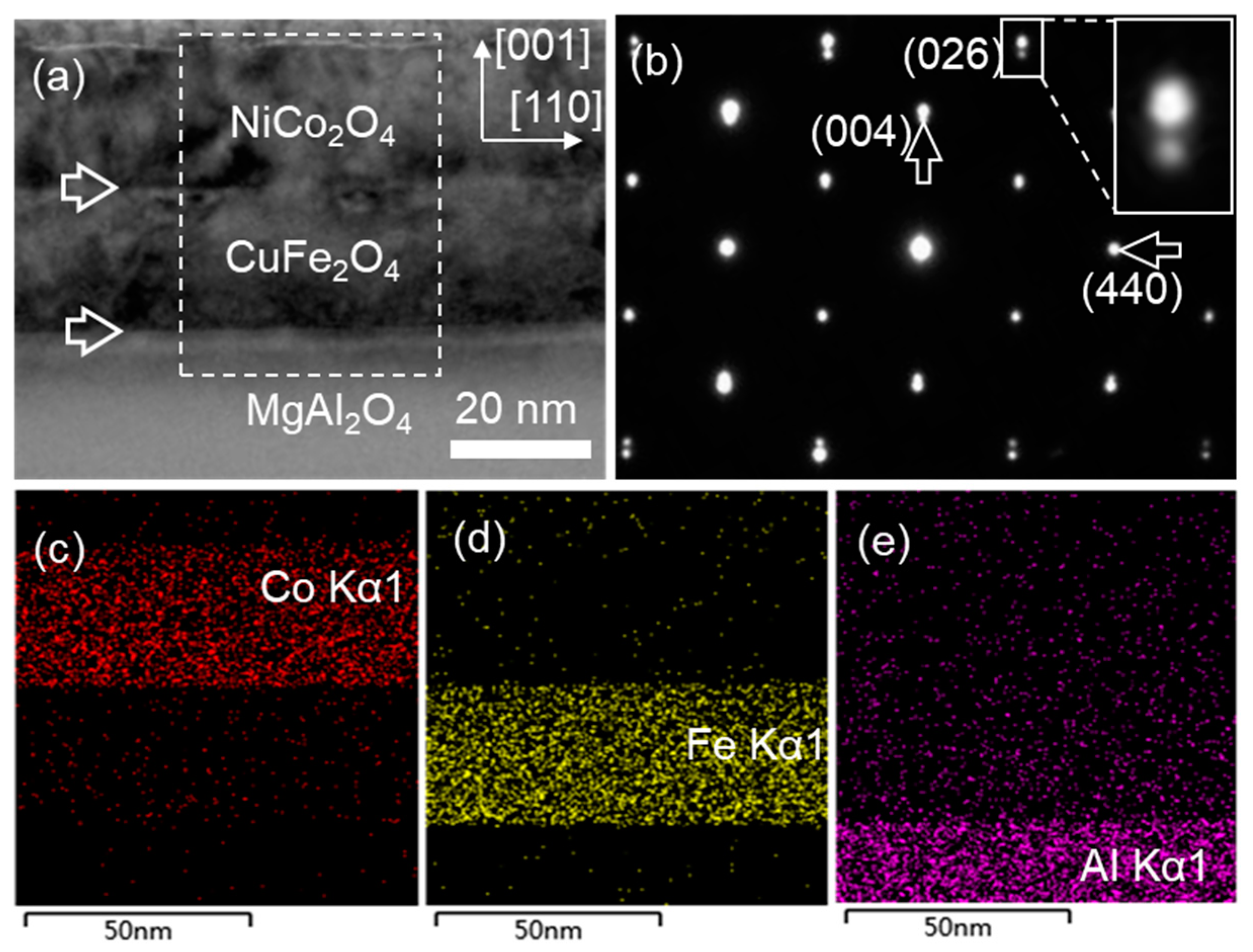
Figure 2.
(a, b) Atomic-resolution HAADF images of the interface between CFO film and MAO substrate and the heterostructure interface of NCO film and CFO film denoted by white dashed line, respectively, showing epitaxially coherently grown on substrate at this region.
Figure 2.
(a, b) Atomic-resolution HAADF images of the interface between CFO film and MAO substrate and the heterostructure interface of NCO film and CFO film denoted by white dashed line, respectively, showing epitaxially coherently grown on substrate at this region.
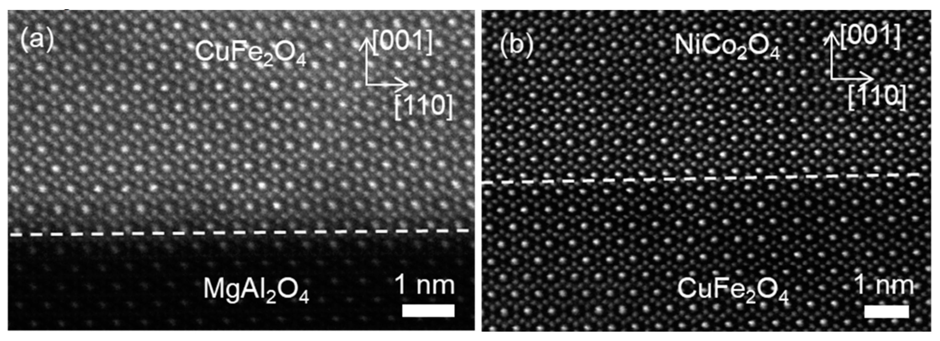
Figure 6.
(a, b) Low-magnification BF-TEM images of NCO/CFO film on MAO (001) substrate. The two kinds of different interface are indicated by horizontal white arrows. (b) The typical SAED pattern of the bilayer heterostructure film, recorded along the [10] MAO zone axes. The splitting of the reflection spots is indicated by the vertical arrows. (c) Atomic-resolution HAADF images of the interface between NCO film and CFO film denoted by white dashed line, showing epitaxially coherently grown on substrate at this region.
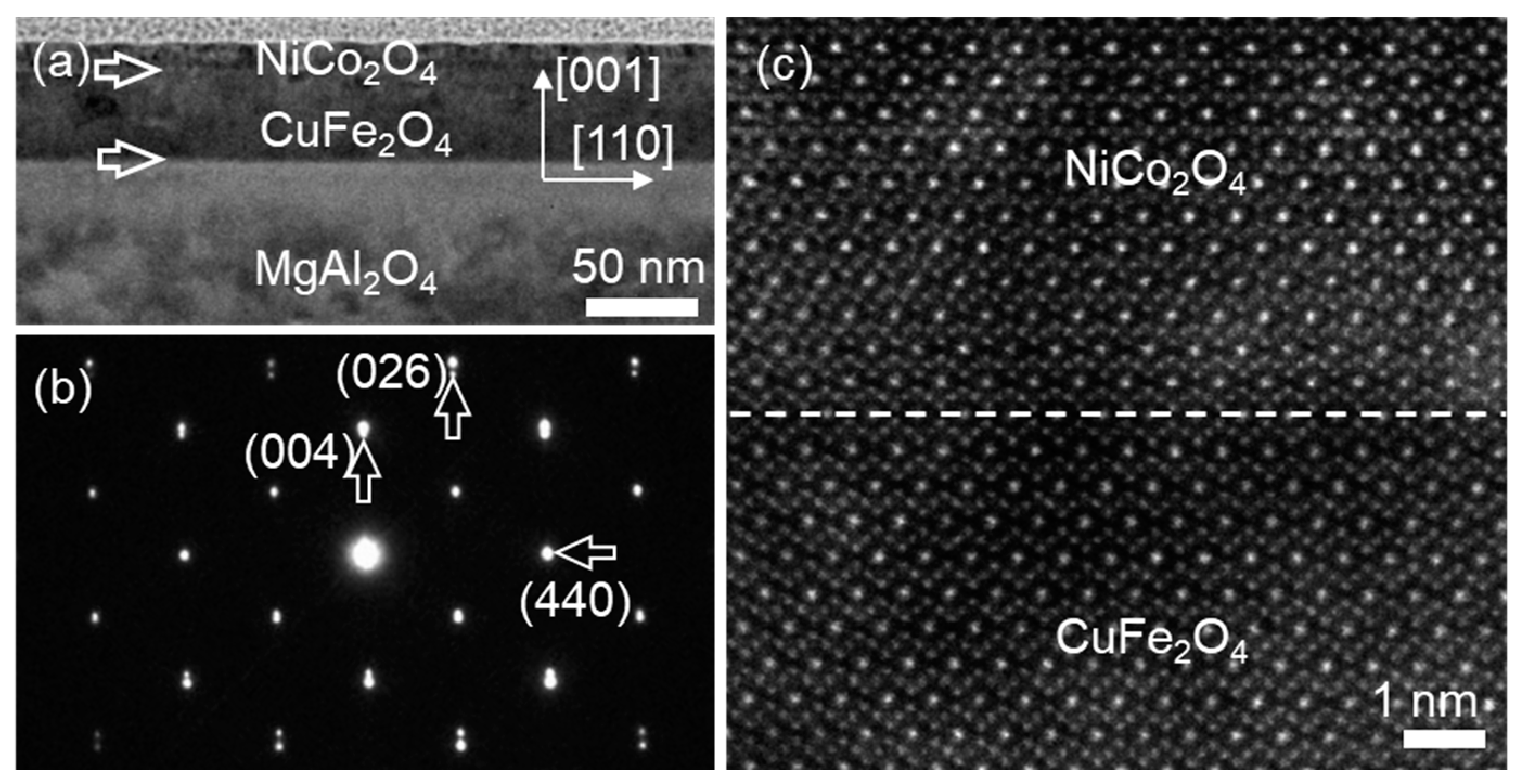
Figure 7.
(a, b) Atomic-resolution HAADF images of the heterostructure interfaces between NCO film and CFO film in different regions denoted by white dashed lines, showing the interfacial dislocations with different Burgers vectors.
Figure 7.
(a, b) Atomic-resolution HAADF images of the heterostructure interfaces between NCO film and CFO film in different regions denoted by white dashed lines, showing the interfacial dislocations with different Burgers vectors.
Disclaimer/Publisher’s Note: The statements, opinions and data contained in all publications are solely those of the individual author(s) and contributor(s) and not of MDPI and/or the editor(s). MDPI and/or the editor(s) disclaim responsibility for any injury to people or property resulting from any ideas, methods, instructions or products referred to in the content. |
© 2024 by the authors. Licensee MDPI, Basel, Switzerland. This article is an open access article distributed under the terms and conditions of the Creative Commons Attribution (CC BY) license (http://creativecommons.org/licenses/by/4.0/).
Copyright: This open access article is published under a Creative Commons CC BY 4.0 license, which permit the free download, distribution, and reuse, provided that the author and preprint are cited in any reuse.


