
Submitted:
06 September 2023
Posted:
07 September 2023
You are already at the latest version
Abstract
Ion beam-assisted deposition (IBAD) has been proposed as a promising texturing technology that uses film epitaxy method to obtain biaxial texture on a non-textured metal or compound substrate. Magnesium oxide (MgO) is the most well explored texturing material. In order to obtain the optimal biaxial texture, the actual thickness of the IBAD-MgO film must be controlled within 12 nm. Due to the bombardment of ion beams, IBAD-MgO has large lattice deformation, poor texture and many defects in the films. In this work, an additional homogeneous epitaxy MgO (epi-MgO) layer has been deposited on the IBAD-MgO layer by electron-beam evaporation. The biaxial texture can be optimized by the deposition of additional epi-MgO layer. The effects of growth temperature, film thickness, deposition rate and oxygen flux on the texture and morphology of the epi-MgO film were systematically studied. After the research of epi-MgO process, the best full width at half maximum (FWHM) values were 2.2 for the out-of-plane texture and 4.8° for the in-plane texture, respectively. Subsequently, the LaMnO3 cap layer and YBa2Cu3O7-x (YBCO) functional layer was deposited on the epi-MgO layer to test the quality of MgO layer. Finally, the critical current density of YBCO films is 6MA/cm2 (77K, 500nm, self-field), indicating that this research provides a high-quality MgO substrate for the YBCO layer.
Keywords:
ion beam-assisted deposition
; magnesium oxide
; homogeneous epitaxy
; fluorene
1. Introduction
YBa2Cu3O7-x (YBCO) superconducting conductors exhibit excellent electrical properties and broad application prospects in the fields of transmission cables, strong magnets, motors, and current limiters [1,2,3,4,5,6]. In order to realize the application of high-temperature superconducting materials in the field of strong electricity, the critical current (Ic) must be as high as 200A/cm [7]; Moreover, the YBCO conductors must be epitaxial growth on cheap metal substrates by the thin film deposition method to increase the mechanical properties [8]. However, the direct deposition of YBCO films on metal substrates causes the diffusion of metal elements from the metal substrate to the superconducting layer [9]. In addition, the oxygen element is easy to diffuse to the metal substrate, thereby reducing the mechanical properties of the metal substrate [10]. Therefore, an oxide buffer layer structure must be introduced between the metal substrate and the superconducting layer [11,12,13,14].
The functions of the buffer layers can be described as follows: Firstly, block the mutual diffusion of elements between the metal substrate and the YBCO layer. The flat and dense oxide buffer films can prevent direct contact between the superconducting layer and the YBCO layer, effectively blocking the mutual diffusion of elements [15,16,17]. Secondly, the adhesion of YBCO layer deposited on oxide buffer layers is much better than that on the metal substrates [18,19,20]. Finally, the biaxial texture required for YBCO growth can be introduced by the film epitaxy method in the oxide buffer layers [21,22,23].
At present, there are three well explored technologies for obtaining biaxial texture, i.e., rolling-assisted biaxial texture, inclined substrate deposition and ion beam-assisted deposition (IBAD) [24]. The biaxial texture can be obtained by the thin film epitaxy method on a non-textured metal or compound substrate in the IBAD technology [25]. The interaction between ions and deposited atoms promotes the grain rearrangement in the buffer layers [26]. There are some critical issues that need to be addressed in the preparation process of buffer layers, including obtaining high-quality biaxial texture [27,28,29], reducing the production costs [30], and improving the uniformity of the buffer layer [31].
In our previous research, we have proposed a promising buffer layer structure for YBCO films, including LaMnO3 (LMO)/IBAD-MgO/Y2O3 multi-layer structure [32]. However, the buffer layer shows poor biaxial texture with the out-of-plane the full width at half maximum (FWHM) value of 3.5° and in-plane FWHM value of 7.2° in the buffer layer, respectively. It should be noted that sufficient critical currents can hardly be obtained with the in-plane texture over 5° [33]. Therefore, it’s necessary to reduce the biaxial texture. Y. Yamada et al. have deposited CeO2 cap layer on IBAD-MgO to improve the biaxial texture. However, the best in-plane FWHM value is 6° in their research [34].
In this paper, we prepared epi-MgO films using electron beam evaporation and systematically investigated the influence of the growth temperature, film thickness, deposition rate, and oxygen flow rate on the texture and morphology of the MgO films. It is necessary to obtain the MgO film with the best biaxial texture, which would provide an excellent growth template for YBCO superconducting thin films. Finally, the LMO cap layer and YBCO superconductor films are fabricated on the MgO films to testify the function of epi-MgO films.
2. Experiment
In this work, electron beam evaporation, which offers the ability to evaporate metal oxide materials with high melting point, was used to deposit epi-MgO films on 10 nm-thick IBAD-MgO films. In this experiment, the vacuum chamber was pumped down to 10-5Pa using a molecular pump. Subsequently, the growth temperature (150°C ~ 500°C) required for the experiment was controlled by a home-made heating device. The MgO homoepitaxial layer was deposited on the substrate using electron beam evaporation from a crucible. A reel-to-reel system enables the continuous preparation of long tapes for the dynamic deposition of the epi-MgO films. The film thickness was characterized in situ using a high-energy electron diffraction (RHEED) equipment. RHEED involves emitting a beam of high-energy electrons (5~100 keV) from an electron gun, which is incident on the sample surface at a small grazing angle (1~5°) to generate an electron diffraction beam. The crystal structure is then displayed by collecting the signal on a fluorescent screen.
The biaxial texture of the epi-MgO films was characterized by θ-2θ scans using X-ray diffraction (XRD). The crystal orientation and crystallinity of the epi-MgO films can be obtained by comparing the θ-2θ scan spectrum with the diffraction spectrum card. The FWHM of the out-of-plane texture and in-plane texture of the epi-MgO films can be obtained by fitting the ω-scan curve and φ-scan curve, respectively. The smaller the FWHM value, the better arrangement of the crystal grains in MgO films can be obtained. Finally, the surface morphologies of the epi-MgO films were analyzed using the SPM 300HV scanning probe platform from Seiko and the INSPECT F50 SEM platform.
3. Results
The growth temperature plays a crucial role in the epitaxial growth of epi-MgO films, influencing both the structure and surface morphology of the films. Figure 1 displays the XRD θ-2θ diffraction patterns of MgO films, which were deposited at different temperatures with a film thickness of 250nm, a deposition rate of 1.2nm/s, and oxygen pressure of 10-2 Pa. The intensity of the MgO (002) diffraction peak is weak at the deposition temperature of 150°C, indicating that this temperature fails to provide sufficient migration energy for the Epi-MgO films to grow along the c-axis orientation. The migration energy of MgO atoms increases with the deposition temperature increasing, resulting in a gradual increase in the peak intensity of the (002) orientation of the film.
Figure 1.
XRD θ-2θ diffraction results of epi-MgO deposited at different temperatures.
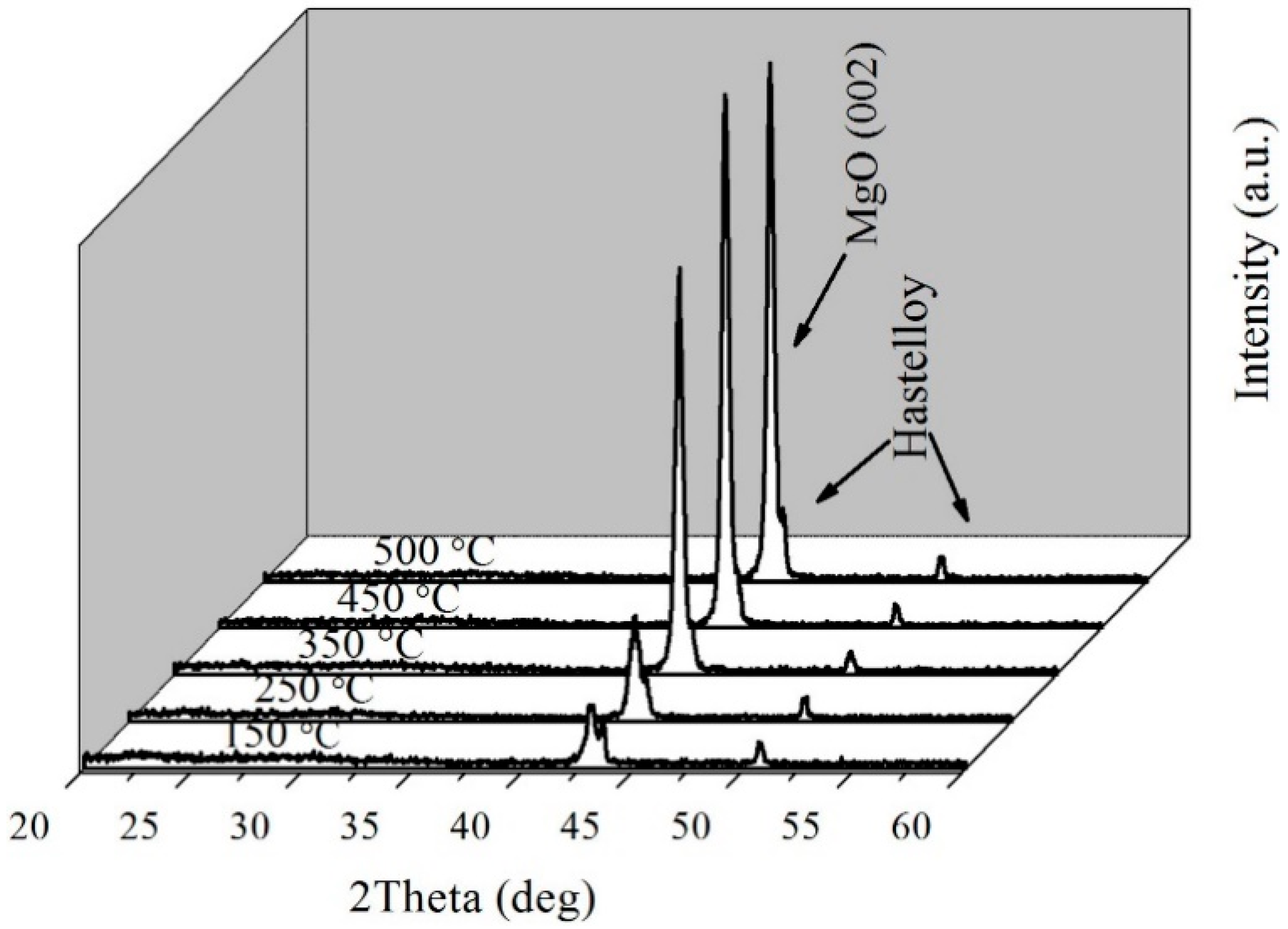
Figure 2 illustrates the variations of the out-of-plane and the in-plane FWHM values of epi-MgO films as a function of the deposition temperature. As shown in the figure, the deposition temperature influences the biaxial texture of the films significantly. The out-of-plane and in-plane FWHM values of the films are 4.6° and 8° at a deposition temperature of 150°C, respectively.
Figure 2.
Half height and width of Epi-MgO prepared at different deposition temperatures.
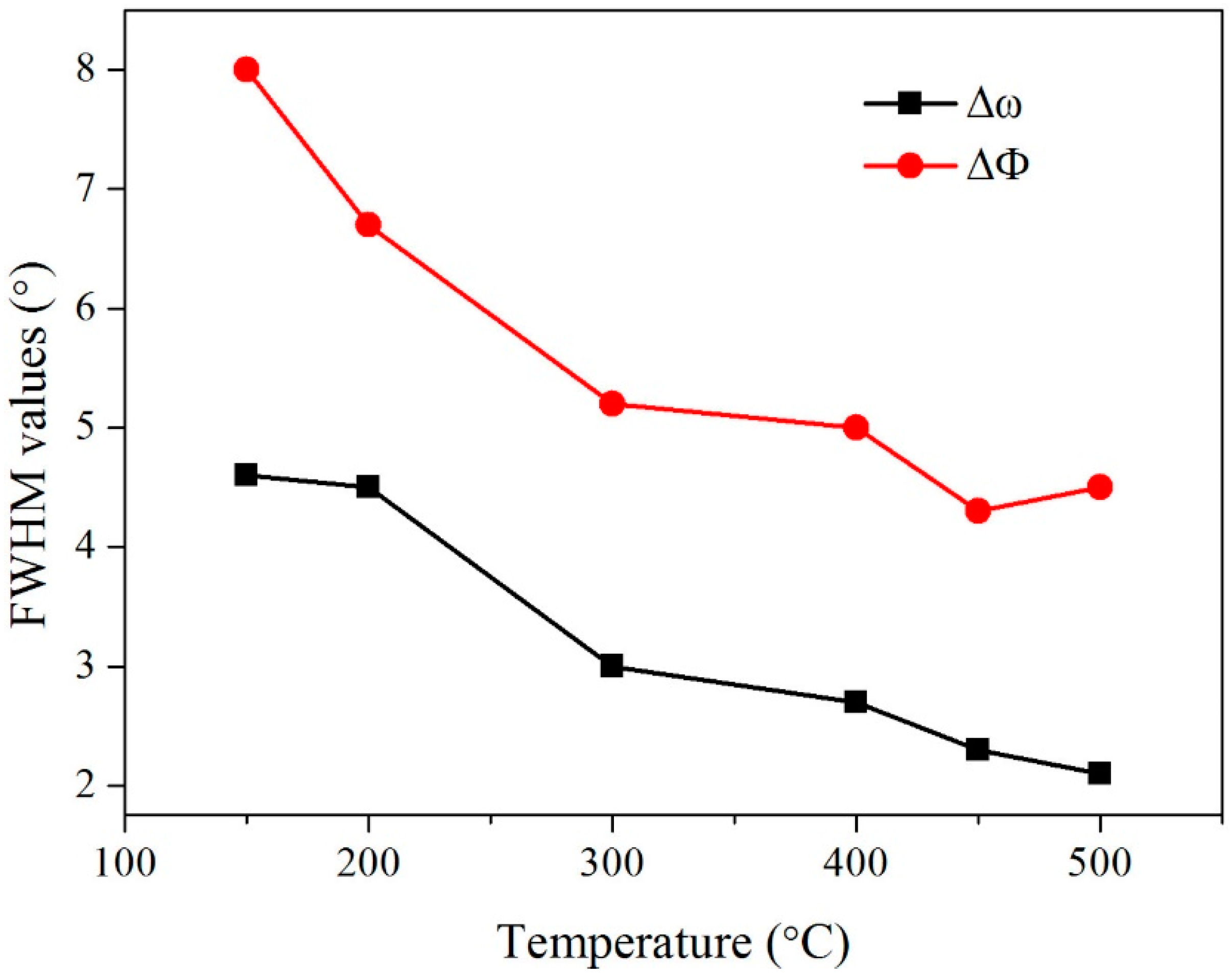
As the deposition temperature gradually increases, both the out-of-plane and in-plane textures are gradually optimized. When the deposition temperature reaches 500°C, the biaxial texture of the epi-MgO films is Δω=2.2° and ΔΦ=4.8°, respectively. It has been proposed that the grain size of MgO increases with the deposition temperature [35]. The large self-epitaxial MgO grains can release the stress in the MgO films between the interface of IBAD-MgO and epi-MgO [36]. Therefore, the epi-MgO films can obtain better biaxial texture at the higher deposition temperature.
When the metal oxide films are prepared using electron beam evaporation, the ionic bonds of the materials can be easily disrupted by the electron beam, potentially causing the composition of the film material to deviate and affecting the microstructure of the film. Therefore, it is necessary to introduce oxygen to maintain the proper proportion of MgO film composition during the epi-MgO deposition process.
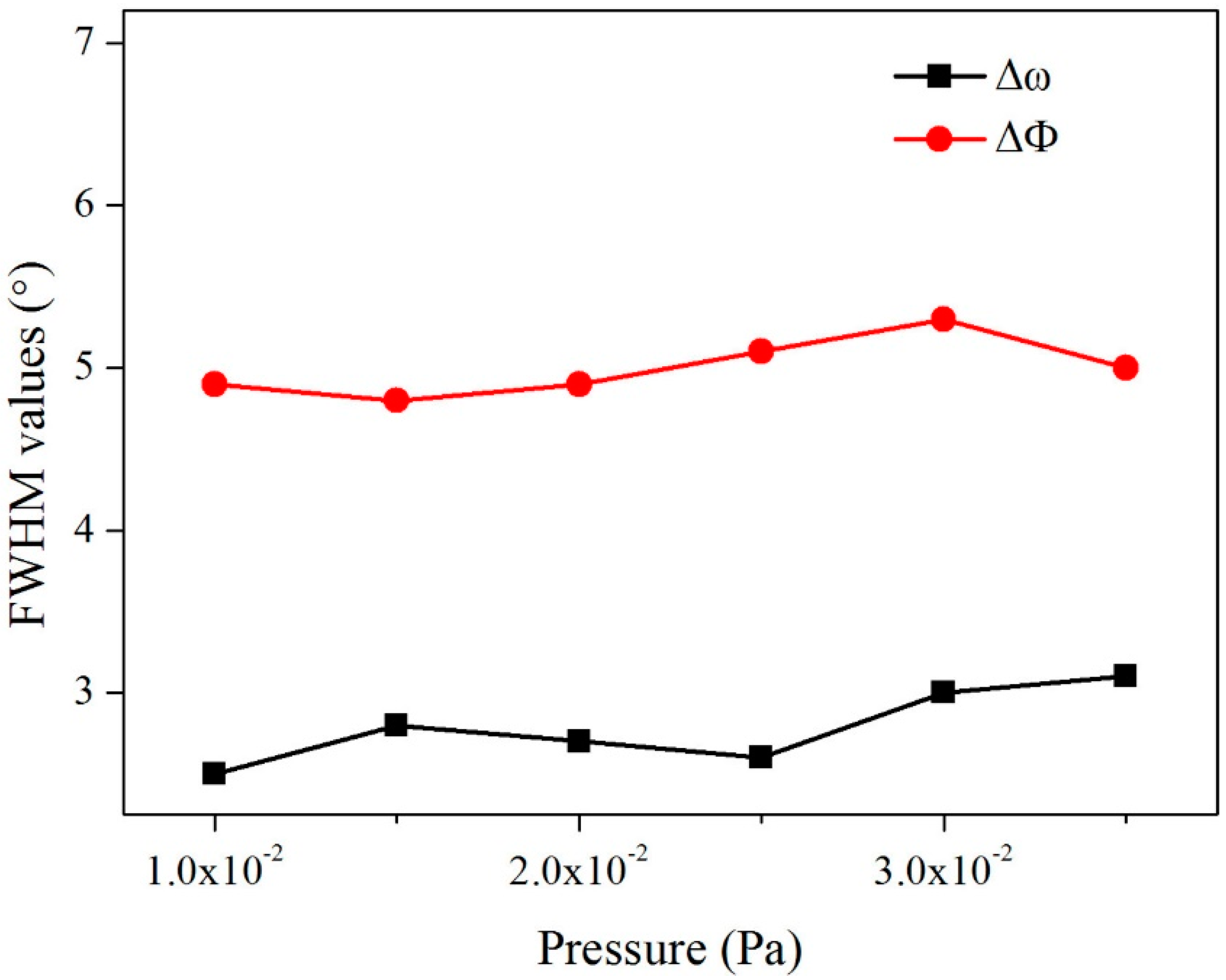
In order to investigate the effect of oxygen flow rate on the MgO films, the epi-MgO films were prepared under different oxygen pressures while keeping other parameters constant with the deposition thickness of 150nm, the growth temperature of 300°C, and deposition rate of 1nm/s. Figure 3 shows the in-plane and out-of-plane FWHM results of the MgO films prepared under different oxygen pressures. We found out that the oxygen flow has little effect on the biaxial texture of MgO.
Figure 3.
the FWHM values of in MgO films with different oxygen flux.
The variation in root mean square roughness (RMS) of the film surface with respect to the oxygen flow rate is illustrated in Figure 4. The RMS of the film surface gradually decreases from 9nm to 4.5nm as the oxygen flow increases from 0 to 3.5x10⁻²Pa, indicating that as the oxygen flow rate increases, the oxygen defects in the film decrease, and the surface morphology is improved.
The deposition rate of the film also has a significant impact on the quality of the Epi-MgO films. By adjusting the electron beam evaporation’s beam current parameters, the film’s deposition rate is changed while keeping the film thickness, deposition temperature, and oxygen flow rate constant. The effect of the deposition rate on the film’s biaxial texture is shown in Figure 5.
Figure 4.
The RMS of MgO films with different oxygen flux: (a) 0; (b) 10-2Pa; (c) 2.5*10-2Pa; (d) 3.5*10-2Pa.
Figure 4.
The RMS of MgO films with different oxygen flux: (a) 0; (b) 10-2Pa; (c) 2.5*10-2Pa; (d) 3.5*10-2Pa.
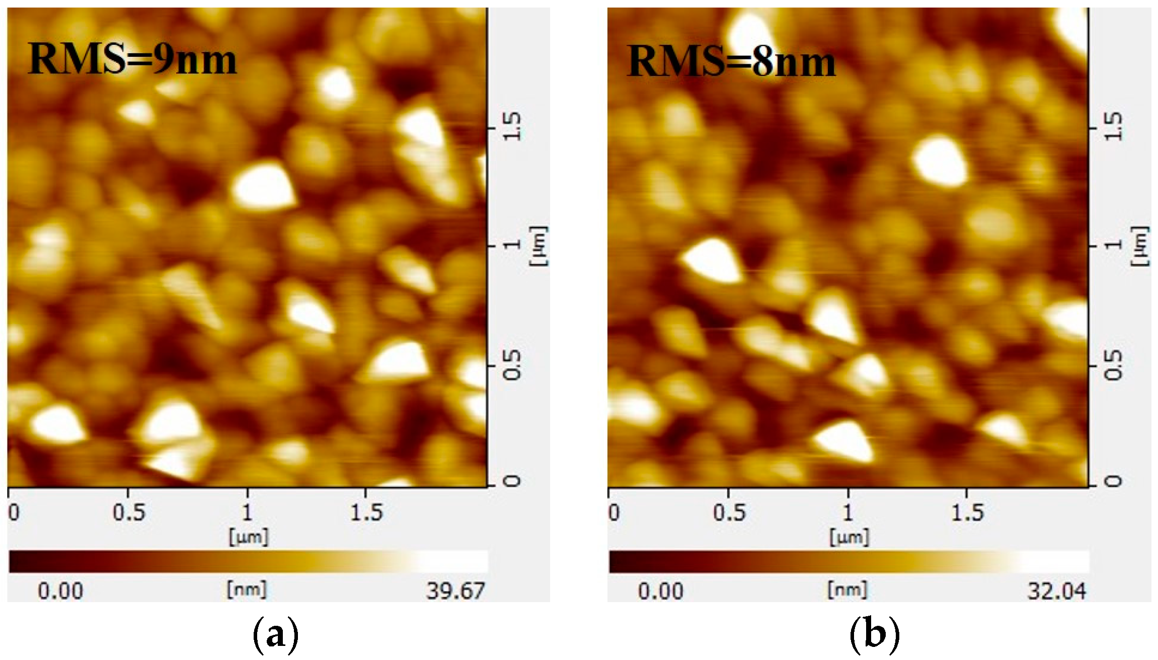
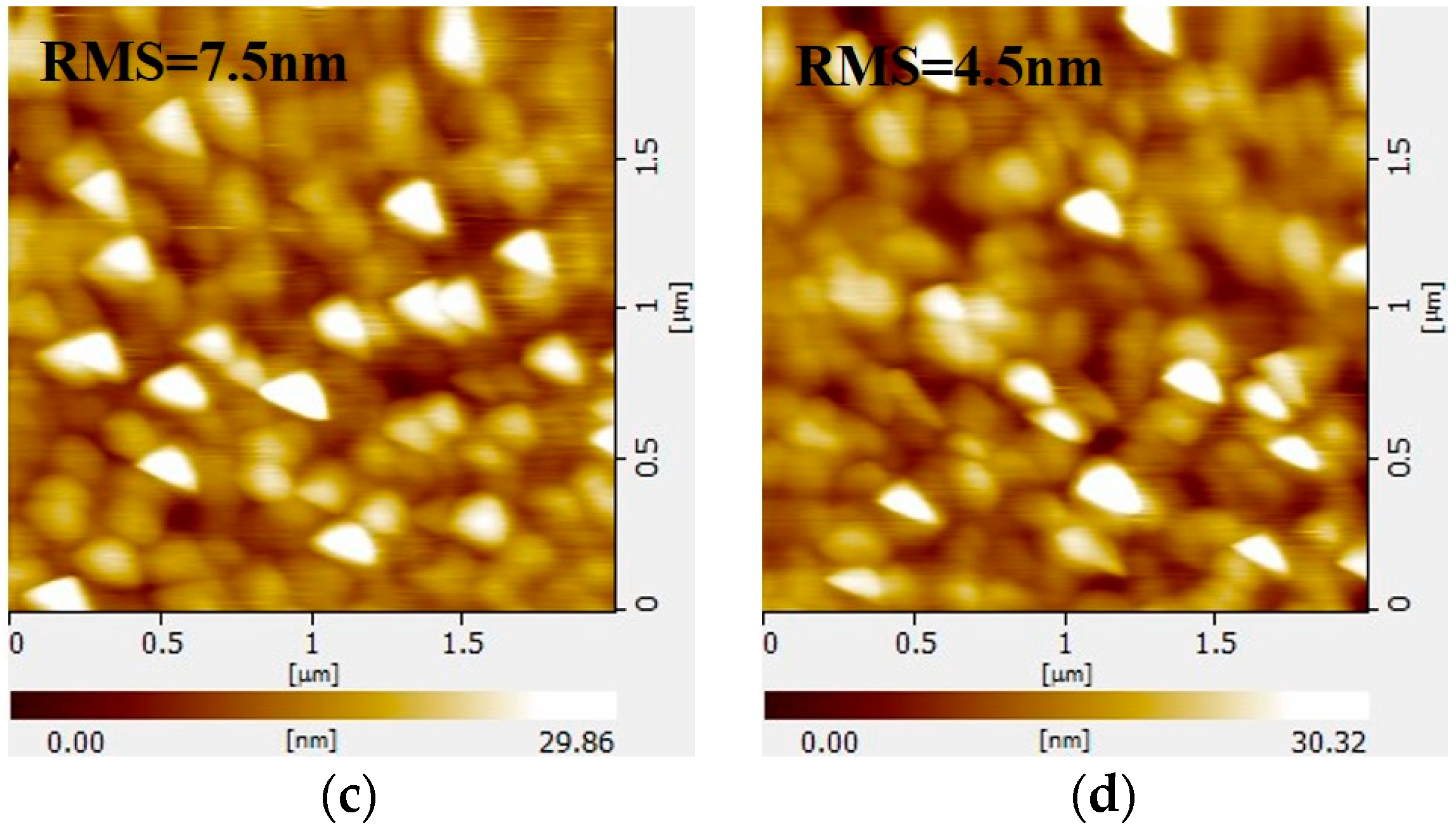
Figure 5.
The texture changes of epi-MgO films with different deposition rates.
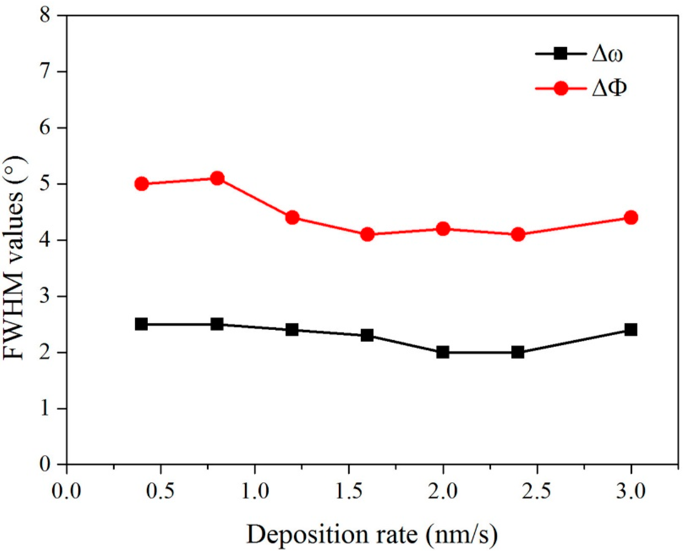
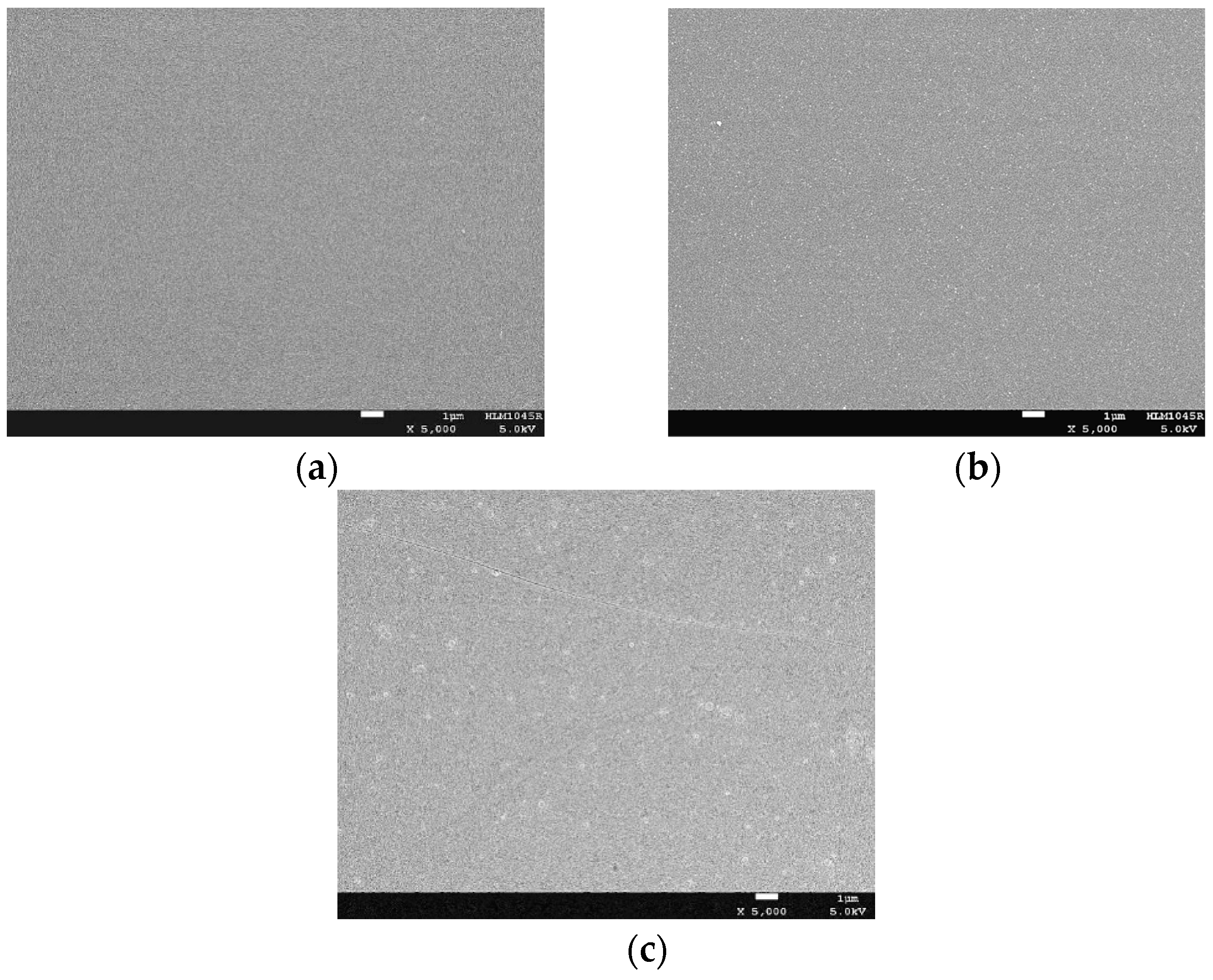
The oxygen flow rate has little effect on the biaxial texture. Subsequently, the surface morphology of these samples was characterized using SEM, and the results are shown in Figure 6. The film surface was smooth and dense with the deposition rate of 0.3nm/s and 1nm/s. When the deposition rate was increased to 3nm/s, some particle agglomerations appeared on the surface. It has been shown that large particles on the film surface have an adverse effect on the superconducting properties of the subsequent YBCO film [37]. Therefore, the film’s deposition rate should not exceed 3nm/s.
Figure 6.
SEM images of Epi-MgO films with different deposition rates. (a) 0.3nm/s; (b) 1nm/s; (c) 3nm/s.
Figure 6.
SEM images of Epi-MgO films with different deposition rates. (a) 0.3nm/s; (b) 1nm/s; (c) 3nm/s.
The thickness is one of the key growth parameters that affect the grain size, crystallinity, and surface morphology of MgO. Figure 7 shows the XRD θ-2θ scan results of Epi-MgO films with the thickness range of 54-720 nm. The film thickness is controlled by the carrier frequency, while other deposition parameters are maintained at a deposition temperature of 450°C, a deposition rate of 1.2 nm/s, and an oxygen flow rate of 1.6×10⁻² Pa. As shown in the figure, an increase in film thickness leads to an enhancement of the crystallinity of MgO, resulting in an increase in the (002) diffraction peak intensity.
The variation of the FWHM values with different thicknesses in the MgO films was analyzed by the ω-scan and φ-scan, as presented in Figure 8, which shows that the in-plane and out-of-plane textures of the film gradually improve with the increase of film thickness. In addition, the RMS roughness of the epi-MgO films varies with the thickness of the film, as shown in Figure 9, where the RMS roughness of the film surface increases with the increase of MgO thickness. These results indicate that the thicker MgO films result in an improvement of the biaxial texture, but the deterioration of the surface morphology.
Figure 7.
The XRD θ-2θ scans of the epi-MgO films with different thickness.
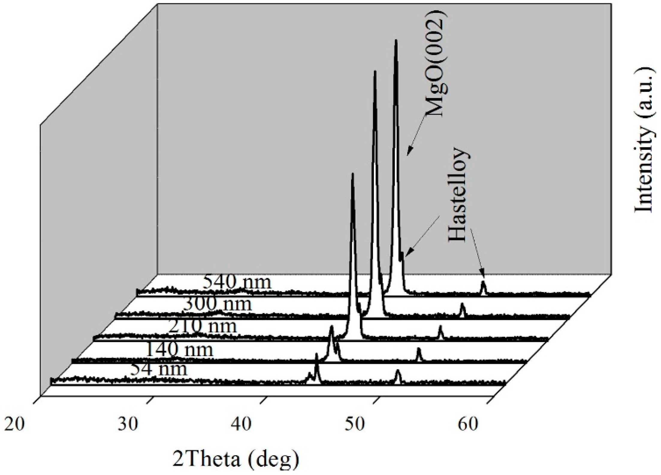
Figure 8.
The in-plane out-plane texture of epi-MgO films with different deposition thicknesses.
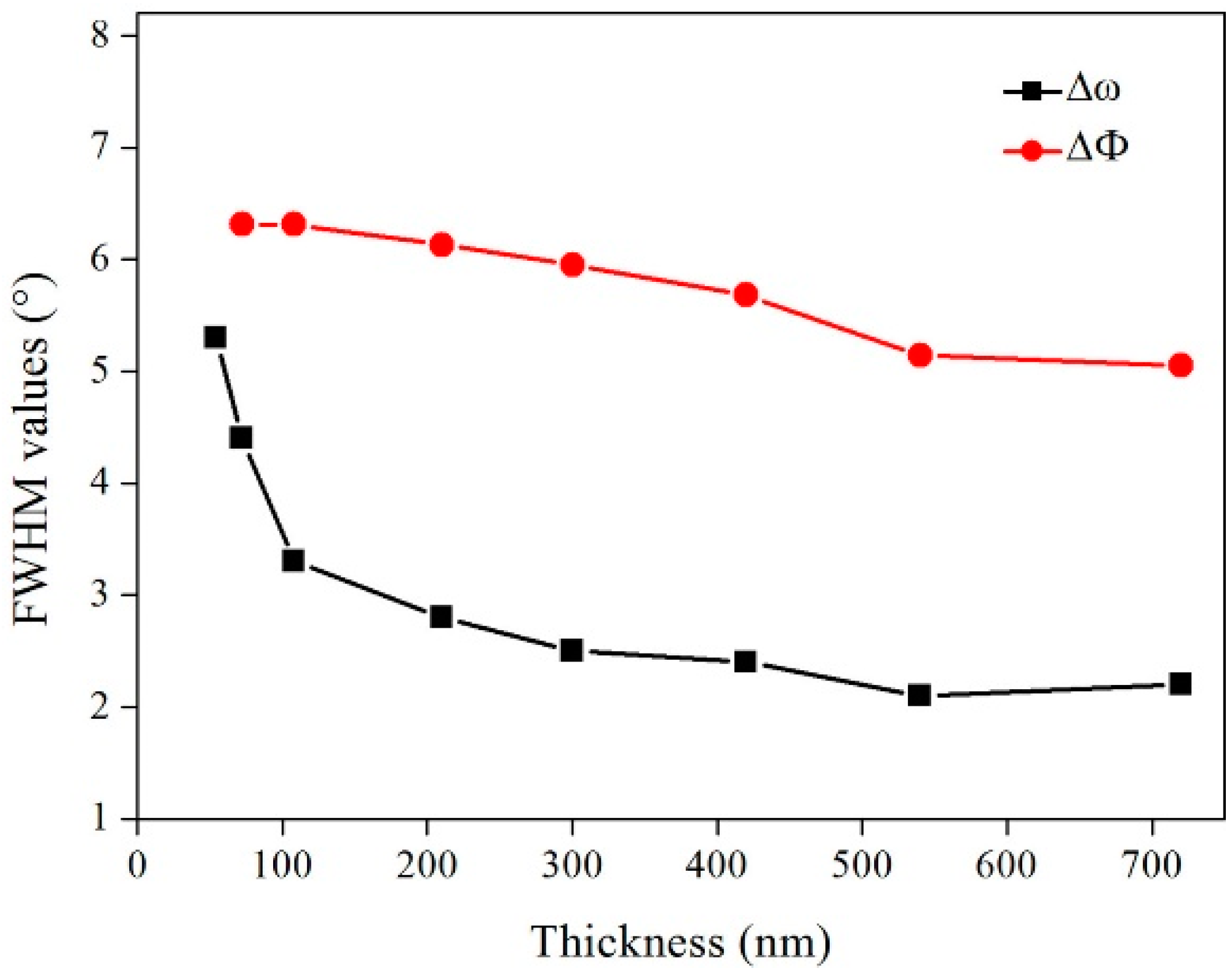
Figure 9.
The surface root-mean-square roughness of epi-MgO films varies with different deposition thicknesses.
Figure 9.
The surface root-mean-square roughness of epi-MgO films varies with different deposition thicknesses.
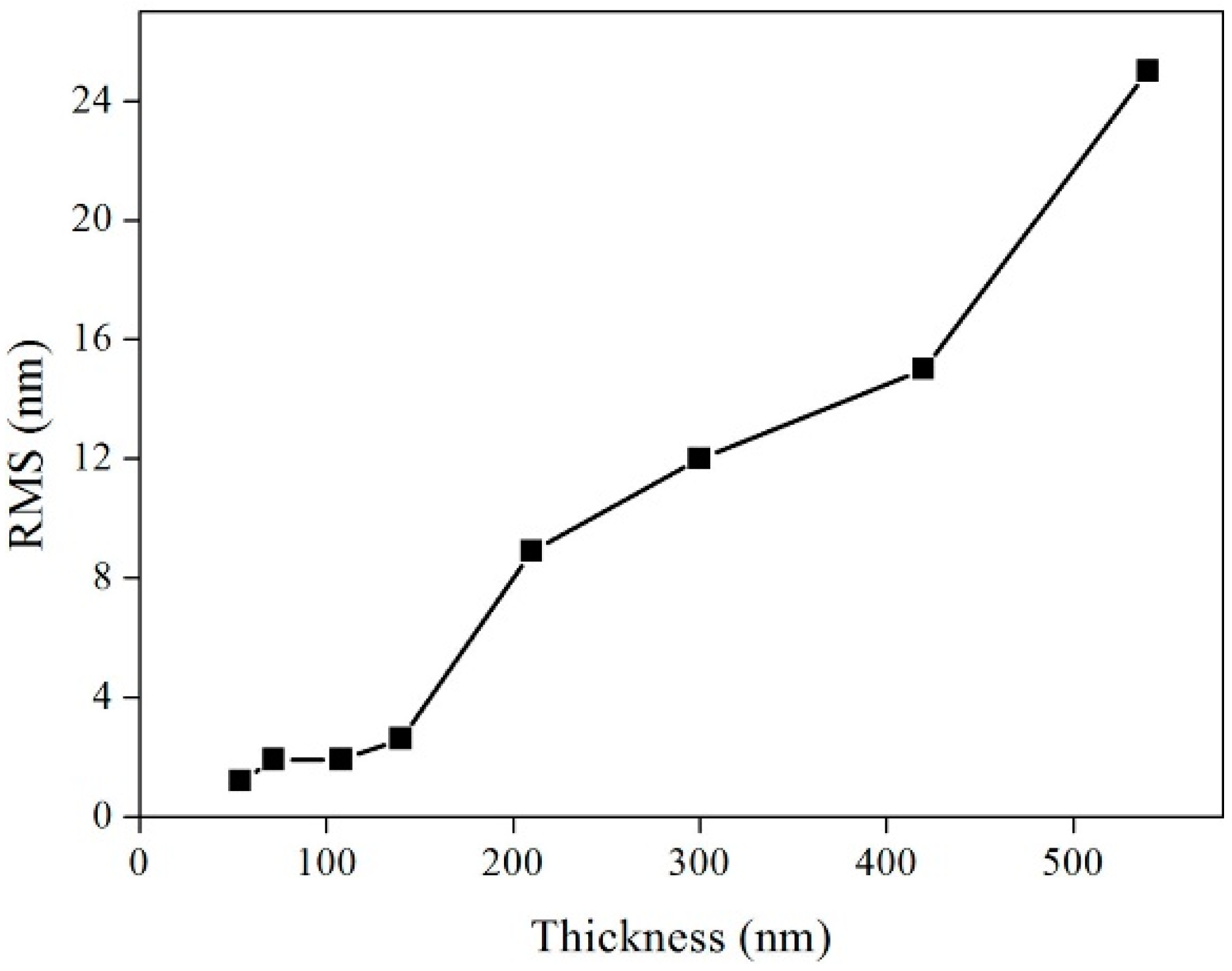
Figure 10a and Figure 10b illustrate the RHEED diffraction patterns of the 10nm-thick IBAD-MgO and 50nm-thick epi-MgO, respectively. It can be observed that the diffraction spots of IBAD-MgO are larger than those of Epi-MgO, suggesting that the epi-MgO films improve the biaxial texture of IBAD-MgO significantly.
Since the lattice mismatch between MgO and the YBCO is relatively high (~8.6%), it is necessary to deposit a template layer between MgO and YBCO. The lattice mismatch between LMO and YBCO is low (~0.8%), which reduces the influence of buffer layer on YBCO growth during the epitaxy process. Subsequently, the YBCO functional layer was deposited on the LMO layer. Figure 11 shows the XRD θ-2θ scan of the YBCO films deposited on the LMO/epi-MgO/IBAD-MgO buffer layers using metal-organic vapor deposition. The diffraction pattern shows that YBCO is growing along the pure c-axis and the (00l) oriented peak intensity is strong.
We use the four-probe method to test the superconductivity of the YBCO films, Figure 12 shows the critical current test diagram of the YBCO film prepared on the LMO/epi-MgO/IBAD-MgO buffer layer. The width of the metal template is 10mm. However, this work can not directly measure the Ic value of the 10mm-wide YBCO tape because of the limitation of current carrying capacity from our current source. The silver electrode can be deposited on the YBCO surface, and the critical current value can be tested. The performance of the 1cm wide superconducting strip is then calculated.
As shown in the Figure 12, the critical current of YBCO films along the silver electrode (0.308mm-width) is 9.27A. It can be calculated that the critical current of this superconducting tape is 301A/cm. After further calculation, the critical current density is 6MA/cm2 (77K, 500nm, self field). The above research shows that high-quality YBCO thin films can be epitaxial grown on the LMO/epi-MgO/IBAD-MgO template.
Figure 10.
RHEED diffraction patterns of the films: (a) IBAD-MgO; (b) Epi-MgO.
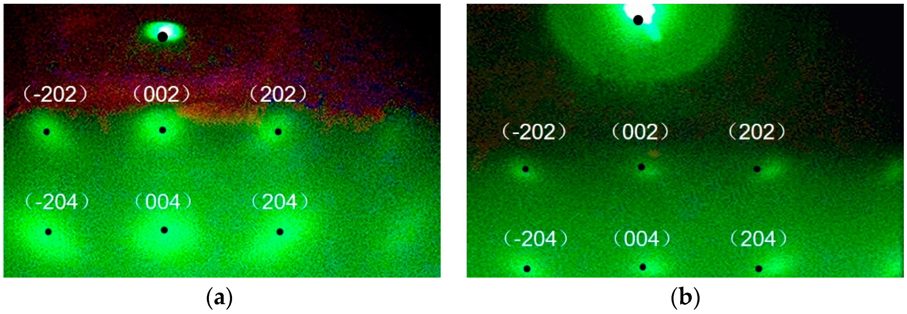
Figure 11.
The XRD θ-2θ scan of YBCO layer.
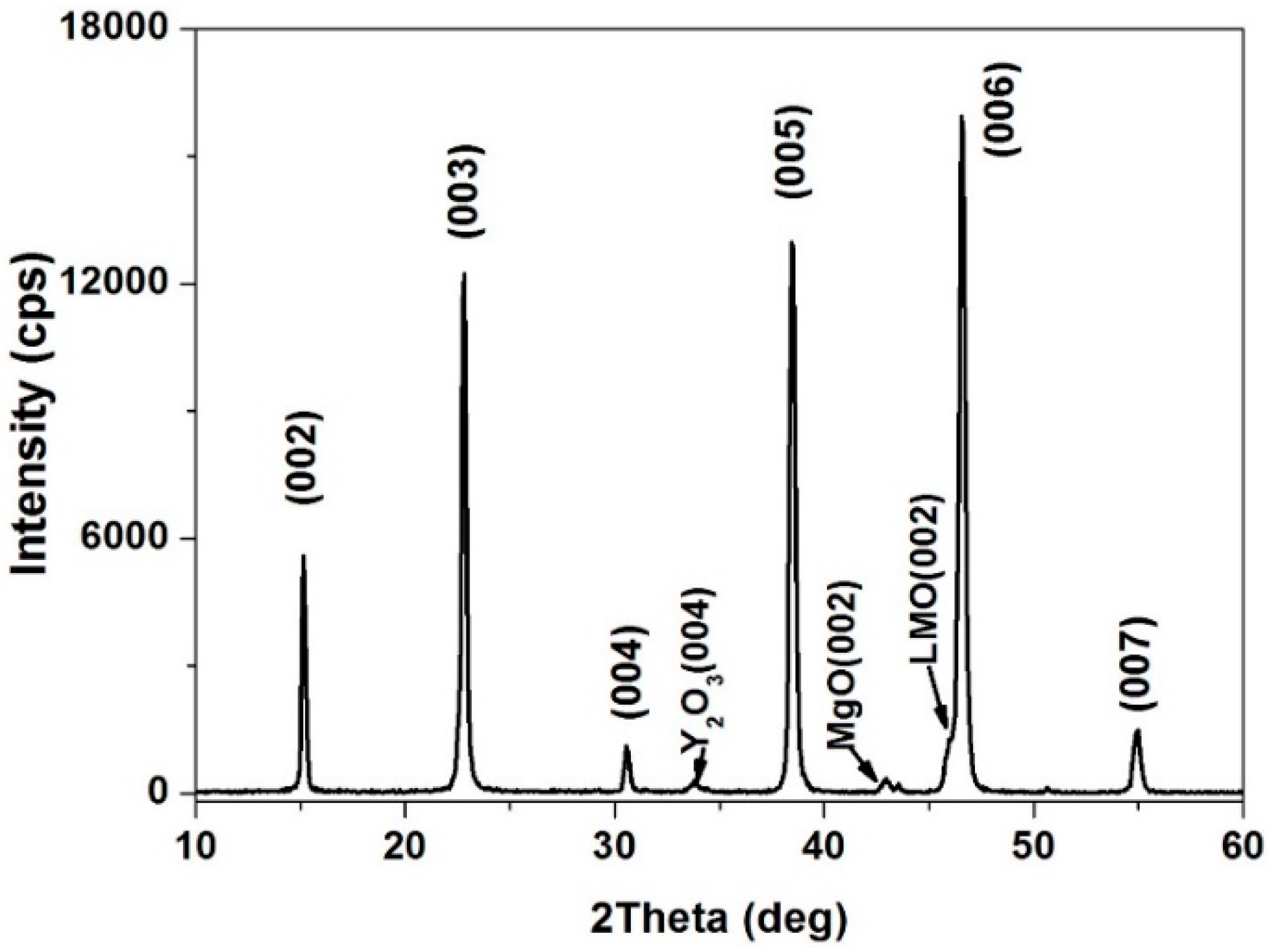
Figure 12.
The I-V characteristic curve of YBCO film under 77K and self-field conditions.

4. Conclusions
This paper investigates the influence of fabrication parameters, such as deposition temperature, film thickness, deposition rate, and oxygen partial pressure, on the structure, texture, and surface morphology of epi-MgO films during the preparation process using IBAD-MgO films as substrates. It has been found out that the crystalline quality of the epi-MgO films has been improved when the deposition temperature was increased from 150°C to 500°C. The out-of-plane FWHM reduces from 4.2° to 2.2°, and the in-plane FWHM decreases from 8° to 4.8°. When the film thickness from 54 nm to 720nm, The RMS value rapidly rises from 1.6nm to 25nm and the in-plane texture increases from 5.4° to 2.2°. The oxygen pressure and deposition rate have a minimal impact on the biaxial texture but significantly affect its surface morphology. The critical current density of YBCO films deposited on the LMO/epi-MgO/IBAD-MgO template is 6MA/cm2 (77K, 500nm, self field), indicating that this research provides a high-quality substrate for the YBCO layer.
Funding
This research received no external funding.
Acknowledgments
We gratefully acknowledge the funding from the Basic and Applied Basic Research Funding of Guangdong (No.2019M650341, No.2020A1515110551), Provincial Education Department of Guangdong (No.2021KTSCX277), the National Natural Science Foundation of China (No.12074264), Provincial High Vocational Education Teaching Reform Research and Practice Project (GDJG2021422), Key funded projects of special funds for scientific and technological innovation strategy of Guangdong Province (pdjh2022a0973, pdjh2022001, pdjh2023a0967) and the Founding of Shenzhen polytechnic (No. 6021310007K, 6022312061K, 6022310034K, 6021271011K, 6021230059K, 6021210078K, LHRC20220402, 1019-8122310001C0, LLJY202306, P-20230703-41376, 7023310168, 7023320062) for this work.
Conflicts of Interest
The authors declare no conflict of interest.
References
- Q. Nie, J. Jiang, H Qu, Yue C, S. Wang, J. Wang, J. Wang, B. Yang, Z. Qing and Y. Xue. Biaxially textured MgO buffer layer on flexible metal template for coated conductor. Journal of Materials Science: Materials in Electronics, 2022, 33(20): 16678-16687. [CrossRef]
- Y. Xue, C. Liao, S. Zhang. Epitaxial growth and characterization of dual-sided Y2O3 buffer layer for superconducting coated conductors. Ceramics International, 2020, 46(15), 23728-23733. [CrossRef]
- Thomas, E. Devaux, K. Nagarajan, G. Rogez, M. Seidel, F. Richard, C. Genet, M. Drillon and T. W. Ebbesen. Large enhancement of ferromagnetism under a collective strong coupling of YBCO nanoparticles. Nano letters, 2021, 21(10): 4365-4370. [CrossRef]
- E. Hannachi, K. A. Mahmoud, M. I. Sayyed and Y. Slimani. Effect of sintering conditions on the radiation shielding characteristics of YBCO superconducting ceramics. Journal of Physics and Chemistry of Solids, 2022, 164: 110627. [CrossRef]
- L. Liu, J. Liu, P. F. Zhai, S. Zhang, J. Zeng, P. Hu, L. Xu and Z. Li. The variation of pinning efficiency in YBCO films containing columnar defects. Physica C: Superconductivity and its Applications, 2022, 592: 1354000. [CrossRef]
- V. Pinto, A. Vannozzi, G. Celentano, M. Tomellini, A. Meledin and S. Orlanducci. Nanodiamond Influence on the Nucleation and Growth of YBCO Superconducting Film Deposited by Metal–Organic Decomposition. Crystal Growth & Design, 2023, 23(8): 6086-6099. [CrossRef]
- M. Yazdani-Asrami, A. Sadeghi, S. M. Seyyedbarzegar and A. Saadat. Advanced experimental-based data-driven model for the electromechanical behavior of twisted YBCO tapes considering thermomagnetic constraints. Superconductor Science and Technology, 2022, 35(5): 054004. [CrossRef]
- J. Hu, J. Ma, J. Yang, M. Tian, A. Shah, I. Patel, H. Wei, L Hao, Y. Ozturk, B. Shen and T. A. Coombs. Numerical study on dynamic resistance of an HTS switch made of series-connected YBCO stacks. IEEE Transactions on Applied Superconductivity, 2021, 31(5): 1-6. [CrossRef]
- Y. Xue, Y. H. Zhang, R. P. Zhao, F. Zhang, Y. M. Lu, C. B. Cai, J. Xiong and B. W. Tao. Biaxial texture evolution in MgO films fabricated using ion beam-assisted deposition. Journal of Electronic Materials, 2016, 45: 3546-3553. [CrossRef]
- M. Dahiya, R. Kumar, D. Kumar and N. Khare. Comparative study of dimensionality and superconducting parameters in YBCO–NaNbO3 nanoparticles-and nanorods-added composite sample from excess conductivity analysis. Applied Physics A, 2022, 128(4): 308. [CrossRef]
- D. Mendes, D. Sousa, A. C. Cerdeira, L. C. J. Pereira, A. Marques, J. Murta-Pina, A. Pronto and I. Ferreira. Low-cost and high-performance 3D printed YBCO superconductors. Ceramics International, 2021, 47(1): 381-387. [CrossRef]
- E. Hannachi, M. I. Sayyed, K. A. Mahmoud and Y. Slimani. Correlation between the structure, grain size distribution and radiation shielding peculiarities of YBCO ceramics prepared by two different milling methods. Applied Physics A, 2022, 128(9): 787. [CrossRef]
- X. Liu, Z. Ke, Y. Cheng, Y. Liu and Z. Deng. Strong magnetic field dependence of micro-YBCO superconductor levitated above Halbach guideway. IEEE Transactions on Instrumentation and Measurement, 2022, 71: 1-10. [CrossRef]
- Y. Gu, C. Cai, Z. Liu, J. Liu, L. Liu and R. Huang. Effect of Ta irradiation on microstructure and current carrying properties of YBCO coated conductors with element doping. Journal of Applied Physics, 2021, 130(8). [CrossRef]
- G. Z. Li and M. Wang. Employment of NdBCO/YBCO/MgO film seed in the infiltration growth technique for fabricating single-grain YBCO bulk superconductors[J]. Journal of Crystal Growth, 2021, 570: 126198.
- E. I. Glushkov, A. V. Chiginev, L. S. Kuzmin and L. S. Revin. A broadband detector based on series YBCO grain boundary Josephson junctions[J]. Beilstein Journal of Nanotechnology, 2022, 13(1): 325-333.
- A. Koblischka-Veneva and M. R. Koblischka. Residual stress/strain analysis of bulk YBCO superconductors using EBSD. IEEE Transactions on Applied Superconductivity, 2021, 32(4): 1-5. [CrossRef]
- R. Hamoudi, A. May, A. Henniche, J. H. Ouyang and A. Guillet. A comparative study of (Ce) and (Gd) doping influence on the superconducting properties of YBCO ceramics. Ceramics International, 2021, 47(18): 25314-25323. [CrossRef]
- E. Hannachi, Y. Slimani, A. T. Okasha, G. Yasin, M. Iqbal, M. Shariq, D. Kaya, F. B. Azzouz and A. Ekicibil. YBCO superconductor added with one-dimensional TiO2 nanostructures: frequency dependencies of AC susceptibility, FC-ZFC magnetization, and pseudo-gap studies. Journal of Alloys and Compounds, 2021, 883: 160887. [CrossRef]
- D. Torsello, D. Gambino, L. Gozzelino, A. Trotta and F. Laviano. Expected radiation environment and damage for YBCO tapes in compact fusion reactors. Superconductor Science and Technology, 2022, 36(1): 014003. [CrossRef]
- S. M. Kumawat, G. D. Dwivedi, P. F. Su, W. S. Shyu, Y. H. Chien, P. W. Su, C. M. Chung, N. D. B. Fernandez, S. J. Sun, C. H. Hsu, S. Yang and H. Chou. Magnetic Field Enhancement in Critical Current and Possible Triplet Superconductivity in LSMO/YBCO/LSMO Heterostructures. The Journal of Physical Chemistry C, 2023, 127(14): 6861-6872. [CrossRef]
- D. Huang, H. Shang, B. Xie, Q. Zou, H. Dong, K. Wang, L. Zhang, H. Gu and F. Ding. An efficient approach for superconducting joint of YBCO coated conductors. Superconductor Science and Technology, 2022, 35(7): 075004. [CrossRef]
- H. Jin, Q. Wu, G. Xiao, C. Zhou, H. Liu, Y. Tan, F. Liu and J. Qin. Bending performance analysis on YBCO cable with high flexibility[J]. Superconductivity, 2023, 7: 100054.
- V. Matias and R. H. Hammond. YBCO superconductor wire based on IBAD-textured templates and RCE of YBCO: Process economics[J]. Physics Procedia, 2012, 36: 1440-1444.
- P. N. Arendt and S. R. Foltyn. Biaxially textured IBAD-MgO templates for YBCO-coated conductors[J]. MRS bulletin, 2004, 29(8): 543-550.
- M. Inoue, T. Kiss, D. Mitsui, T. Nakamura, T. Fujiwara, S. Awaji, K. Watanabe, A. Ibi, S. Miyata, Y. Yamada and Y. Shiohara. Current transport properties of 200 A-200 m-class IBAD YBCO coated conductor over wide range of magnetic field and temperature[J]. IEEE transactions on applied superconductivity, 2007, 17(2): 3207-3210.
- A. Ibi, H. Iwai, K. Takahashi, T. Muroga, S. Miyata, T. Watanabe, Y. Yamada and Y. Shiohara. Investigations of thick YBCO coated conductor with high critical current using IBAD-PLD method[J]. Physica C: Superconductivity and its applications, 2005, 426: 910-914.
- Ibi, H. Fukushima, R. Kuriki, S. Miyata, K. Takahashi, H. Kobayashi, M. Konishi, T. Watanabe, Y. Yamada and Y. Shiohara. Development of long YBCO coated conductors by IBAD–PLD method[J]. Physica C: Superconductivity and its applications, 2006, 445: 525-528.
- P. N.Arendt, S. R. Foltyn, L. Civale, R. F. DePaula, P. C. Dowden, J. R. Groves, T. G. Holesinger, Q. X. Jia, S. Kreiskott, L. Stan, I. Usov, H. wang and J. Y. Coulter. High critical current YBCO coated conductors based on IBAD MgO[J]. Physica C: Superconductivity, 2004, 412: 795-800.
- V. Matias, E. J. Rowley, Y. Coulter, B. Maiorov, T. Holesinger, C. Yung, V. Glyantsev and B. Moeckly. YBCO films grown by reactive co-evaporation on simplified IBAD-MgO coated conductor templates[J]. Superconductor Science and Technology, 2009, 23(1): 014018.
- J. R. Groves, P. N. Arendt, S. R. Foltyn, Q. X. Jia, T. G. Holesinger, L. A. Emmert, R. F. DePaula, P. C. Dowden and L. Stan. Improvement of IBAD MgO template layers on metallic substrates for YBCO HTS deposition[J]. IEEE transactions on applied superconductivity, 2003, 13(2): 2651-2654.
- Y. Xue, Y. H. Zhang, F. Zhang, R. P. Zhao, H. Wang, J. Xiong and B. W. Tao. Growth of simplified buffer template on flexible metallic substrates for YBCO coated conductors[J]. Journal of Alloys and Compounds. 2016, 673:47-53.
- R. Liang, P. Dosanjh, D. A. Bonn, D. J. Baar, J. F. Carolan and W. N. Hardy. Growth and properties of superconducting YBCO single crystals[J]. Physica C: Superconductivity, 1992, 195(1-2): 51-58.
- Y. Yamada, T. Muroga, H. Iwai, T. Izumi and Y. Shiohara. Present status and perspective of IBAD and PLD system in SRL and self-epitaxy in PLD-CeO2 on IBAD seed layer[J]. Physica C: Superconductivity, 2003, 392: 777-782.
- Q. Luo, L. Liu, G. Xiao and Y. Li. Preparation of epitaxial MgO films deposited by RF magnetic sputtering on the IBAD-MgO substrate. Journal of Superconductivity & Novel Magnetism, 2014, 27(6):1419-1424. [CrossRef]
- T. Taneda, M. Yoshizumi, T. Takahashi, R. Kuriki, T. Shinozaki, T. Izumi, Y. Shiohara, Y. Iijima, T. Saitoh, R. Yoshida, T. Kato, T. Hirayama and T. Kiss. Mechanism of Self-Epitaxy in Buffer Layer for Coated Conductors[J]. IEEE Transactions on Applied Superconductivity, 2013, 23(3):6601005-6601005.
- Q. Luo, L. Liu, G. Xiao and Y. Li. Effect of the O2/Arpressure ratio on the microstructure and surface morphology of Epi-MgO/IBAD-MgO templates for GdBa2Cu3O7-δ coated conductors[J]. Chinese Physics Letters, 2014, 31(3):160-163.
Disclaimer/Publisher’s Note: The statements, opinions and data contained in all publications are solely those of the individual author(s) and contributor(s) and not of MDPI and/or the editor(s). MDPI and/or the editor(s) disclaim responsibility for any injury to people or property resulting from any ideas, methods, instructions or products referred to in the content. |
© 2023 by the authors. Licensee MDPI, Basel, Switzerland. This article is an open access article distributed under the terms and conditions of the Creative Commons Attribution (CC BY) license (http://creativecommons.org/licenses/by/4.0/).
Copyright: This open access article is published under a Creative Commons CC BY 4.0 license, which permit the free download, distribution, and reuse, provided that the author and preprint are cited in any reuse.


