Submitted:
13 November 2024
Posted:
14 November 2024
Read the latest preprint version here
Abstract
This paper introduces an innovative energy circuit that challenges conventional understandings of energy conservation, marking a significant departure from traditional frameworks. Seeking to enhance energy generation within existing paradigms, this innovation holds promise for addressing pressing global issues such as the energy crisis and environmental sustainability, while also stimulating scientific inquiry. In contrast to prevalent misconceptions rooted in philosophical and scientific constraints, this study refutes the notion of generating energy from nothing and questions the viability of perpetual motion machines as conceptual models. Instead, it proposes a novel circuit design derived from an unconventional electrical short circuit, which is shown to disrupt the established principles of energy conservation. This circuit offers a transformative approach with diverse applications, including self-recharging capabilities for electric vehicles, bolstering microgrid infrastructure, and facilitating the integration of renewable energy sources. Transcending conventional scientific boundaries, this paper prompts philosophical reflections on the evolving nature of scientific exploration. Ultimately, the energy circuit represents a pivotal step towards mitigating the global energy crisis by reducing reliance on finite resources and fostering sustainability. The paper concludes by illustrating the circuit's potential to revolutionize energy systems and contribute to a more resilient and sustainable future.
Keywords:
energy conservation
; circuit
; electrical short circuit
; energy generation
; energy efficiency
; renewable energy
; self-recharging circuits
; thermodynamics
; electric vehicles
; carbon footprint reduction
1. Introduction
Addressing the pressing energy crisis has been a paramount goal driving numerous innovations and scientific endeavors [1,2]. With declining fossil fuel reserves, environmental degradation, and a increasing global population, the quest for sustainable and abundant energy sources has never been more critical [3,4,5,6]. The potential challenge to the law of energy conservation within classical settings offers a promising avenue to tackle myriad societal challenges, from alleviating the energy crisis to reducing noise pollution from fossil fuel consumption, curbing greenhouse gas emissions, and advancing knowledge in physics and engineering. Recent endeavors to challenge the law of energy conservation have been marred by misconceptions, ranging from the unsubstantiated claims of perpetual motion machines (PMMs) capable of generating infinite energy ([7,8,9]) to the assertion that creating energy within a classical closed system is fundamentally impossible ([10,11,12]). These misconceptions, often grounded in conventional scientific beliefs, have constrained exploration in the search for innovative energy solutions. Consequently, this paper aims to provide a fresh perspective by identifying and correcting prevailing misconceptions surrounding attempts to breaking the law of energy conservation, as exemplified by ([7,9,13,14,15]). The prevalent misconceptions surrounding the generation of energy without external sources are scrutinized in this paper from both scientific and philosophical perspectives. One common misunderstanding challenges the fundamental philosophical principle asserting that “something cannot come from nothing [16,17]”. It is argued that reconciling the creation of energy within a closed system with this philosophical tenet is essential. Additionally, concerns are raised regarding the widely held belief that the absence of PMMs serves as conclusive evidence against the violation of the law of energy conservation [18], implying that energy cannot be created. This paper questions this assumption by highlighting the inherent contradiction within the concept of deriving energy from nothingness. Furthermore, the reliance on PMMs as perfect models to demonstrate the impossibility of breaking the law of energy conservation is challenged. It is argued that such a perspective overlooks the necessity of a machine with 100% efficiency, where energy is neither lost nor gained, in order to substantiate the violation of the law. The paper prioritizes the practicality of a hypothetical system over the mere act of violating a law. It argues that treating experiments, especially those related to energy creation or generation, as purely inductive processes, particularly when considering systems modeled after Perpetual Motion Machines, is flawed. Experiments are grounded in specific empirical observations and cannot be solely refuted by inductive reasoning. Therefore, breaking the law of energy conservation requires the invention of novel methods or a combination of conventional and unconventional approaches to integrate new energy generation techniques with existing engineering and science systems. This perspective challenges the conventional understanding of the energy conservation principle, as methods within current frameworks are unlikely to circumvent the law. An anomalous experiment is proposed: measuring the electrical short circuit current and its impact on an electrical energy system. The paper aims to introduce a hybrid experimental approach, combining conventional and unconventional designs, with a specific focus on using the electrical short circuit as a potential source for excess energy creation, given some energy input. This approach offers several novelties, including: the first experiment to measure and characterize electrical short circuit current in a classical circuit energy system; the first experimental framework demonstrating potential energy creation, violating the law of energy conservation; and a method to transition an electrical energy system from non-ohmic to ohmic behavior for compatibility with current engineering systems. The paper presents an innovative circuit design that challenges the law of energy conservation. This unique design deviates from conventional electrical systems, transitioning from an anomalous state to more traditional circuits.
Leveraging a modified version of Ohm's Law that has been proven to predict electrical short circuit current, [19], the proposed energy circuit originates from an electrical short circuit. This approach challenges the conventions of traditional energy generation systems. While concerns may arise about the proposed solution, as is common with any innovative electric circuit, the experimental results demonstrate that the assumption of a continuously increasing electrical short circuit current during a short circuit is incorrect. In fact, the obtained results show that electrical short circuit current can be measured as a constant quantity. The proposed circuit design incorporated considerable safety measures, and this paper reports with confidence that electrical short circuit current can be measured for a longer duration without destroying the energy system itself. It is essential to highlight the numerous benefits this solution brings to our present society. From transforming electric vehicles to addressing contemporary challenges, the potential applications of this innovative circuit are vast and promising. The journey towards challenging the law of energy conservation extends beyond mere violation of the law itself; it involves exploring concepts of energy destruction, creation, or a blend of both. Such feats may require harnessing scientific anomalies like the electrical short circuit discussed in this paper.
1.1. Analogical Insights and Limitations of Energy Conservation
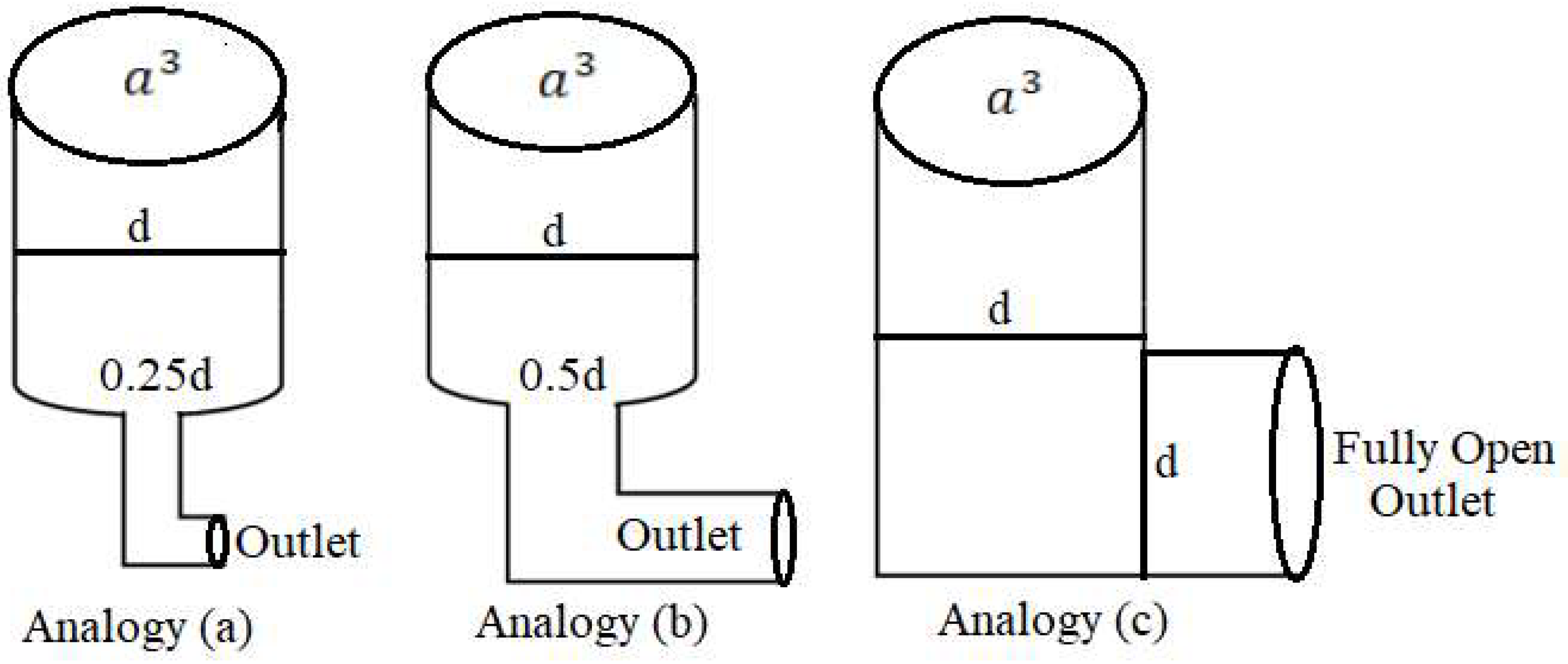
The law of energy conservation, often understood as the impossibility of creating or destroying energy, can be illustrated by a simple analogy: Imagine a sealed room filled with a fixed number of inert cubes. Over time, the number of cubes remains constant, even when checked periodically. This analogy reflects the fundamental principle that energy is conserved, as stated in [12]. To extend this understanding to the electrical domain, consider a water tank analogy. Imagine having three cylindrical tanks of equal diameter () and volume () filled with water. Each tank has a different bottom outlet configuration: one with a small opening (by diameter) (Figure (1) –Analogy (a)), one partially open (by diameter) (Figure (1) –Analogy (b)), and one fully open (Figure (1) –Analogy (c)). Intuitively, it is expected that water flows fastest from the fully open tank. This scenario corresponds to the current incorrect notion of an ideal short circuit in physics, a circuit that offers no resistance to current flow. Through varying the geometries of the containers, we can still observe the current false empirical perspective truth of the law of energy conservation at play. Despite differences in flow rates due to varying bottom outlets (corresponding to varying resistances in electrical conductors), the total energy within the system is assumed to remain constant. This observation underscores the practical limitation of the notion of zero resistance leading to infinite current. It is even a misleading notion to imagine that at zero resistance, the maximum electric current output from such a configuration will be 100%. In reality, such idealized scenarios do not manifest, and there are always practical limitations and resistances that affect current flow as argued by [19,20,21]. The presence of a material’s resistivity property contradicts a zero-resistance current flow, because every electrical conductor will have some non-negligible amount of resistance. This must be true because assuming a zero resistance implies a conductor with no geometric properties such as cross-sectional area and hence some length. Therefore, this new perspective necessitates the development of electrical models that account for the realism of physical quantities such as an electrical current in all possible experimental scenarios. To model concepts like electrical short circuits practically, a modified formulation of Ohm's Law, as proposed recently by [19], is employed. Appendix A provides a detailed justification for this approach, demonstrating its suitability for computing and measuring short circuit currents. By incorporating real-world factors, this modified law offers a more precise framework for analyzing electrical systems compared to the traditional Ohm's Law. Crucially, this paper posits that violating the law of energy conservation encompasses not only the creation of energy ex nihilo but also the attainment of energy conversion efficiencies exceeding 100%. This distinction is pivotal, as it challenges the prevailing unsubstantiated notion that developing a Perpetual Motion Machine (PMM) necessitates a direct violation of energy conservation [12]. The absence of a clear correlation between achieving efficiencies exceeding 100% and the creation of a PMM prompts a reassessment of the validity of using the PMM as definitive proof of the law’s inviolability. This paper contends that achieving 100% efficiency does not equate to energy creation. The presented models, whether employing solid cubes or the water tank-electric charge model, aims at demonstrating that energy within a system is conserved. It is not gained or lost, but rather redistributed or transformed. This paper offers a novel theoretical and practical perspective on challenging the traditional interpretation of energy conservation, focusing on the exploitation of electrical short circuits, a resistance-dependent electrical concept that has not been explored in current studies. Instead of pursuing PMMs, this approach delves into the scientific and philosophical underpinnings of energy conservation and generation. Subsequent sections will explore these concepts in detail, culminating in the presentation of the innovative energy-circuit as a concrete example.
Figure 1.
Illustration of Electric Current-Water Tank Configurations Analogy. (The figures depict cylindrical tanks filled with water, where varying degrees of bottom openings result in different flow rates. The configurations (Analogy (a)-Tank with bottom partially open (by diameter), Analogy (b)-Tank with bottom partially open (by diameter) and Analogy (c)-represents a tank with a fully open bottom. This last configuration serves as an analogy to the current understanding of an electrical short circuit, a circuit with minimal resistance to current flow).
1.2. Review of Related Work
Efforts to challenge the law of energy conservation have undergone significant evolution over time, ranging from initial, well-intentioned investigations to increasingly audacious and unworkable innovations. This complex terrain is revealed through a thorough examination of ongoing studies and objectives, encompassing scientific, philosophical, historical, and contemporary viewpoints [22,23,24]. This paper aims at shedding light on the changing nature of the challenge and exposes prevalent misconceptions and misguided approaches.
1.2.1. Scientific Perspective
Scientific endeavors challenging the law of energy conservation often stem from a misconception about the nature of energy [25,26]. Energy conservation is not merely a convention but a fundamental principle, [26]. Energy is inseparable from the essence of the universe, and attempts to generate energy from nothing contradict current cosmological understanding [27,28]. The scientific community generally considers such efforts futile and flawed. The continued misinterpretations of perpetual motion machines (PMMs) contribute to the misunderstanding portrayed in the current studies, [7,14]. However, this paper presents a contrasting perspective: the absence of a PMM does not necessarily prove that the law of energy conservation can be violated. The criteria for a PMM involve not only violating the law but also creating perpetual motion, a significant challenge in itself. Indeed, this paper argues that there is currently no rigorous theoretical or practical evidence that correlates the development of PMMs with the creation of energy, as desired in the perspective of having an unending energy source or excess energy output from a given energy input. The paper strongly believes that the concept of PMMs stems from a false premise when aligned with the concept of energy, and that the relationship between the two requires careful revision. Overall, the current misconceptions surrounding the concept of energy hinder understanding of how to violate the law of energy conservation.
1.2.2. Philosophical Perspective
The philosophical underpinnings of energy conservation are deeply intertwined with fundamental questions about existence, causation, and the nature of reality. Central to this inquiry is the principle of ex nihilo nihil fit – “nothing comes from nothing” [29,30]. This metaphysical axiom profoundly influences scientific understanding of energy, including its generation and conservation. The proposition of creating energy within a closed system inherently challenges this principle, necessitating a rigorous examination of its philosophical implications. The concept of infinity, a cornerstone of mathematics, introduces a complex dimension to this discourse [31]. While mathematics permits the abstraction of infinity as a limitless quantity, its physical manifestation remains elusive [32]. The paradox of infinite current at zero resistance exemplifies this tension between the mathematical ideal and the constraints of the physical world. This paper posits that infinity, when applied to physical systems, is not a tangible entity but rather a conceptual limit. The Modified Ohm’s Law ([19]) introduced in this paper provides an empirical foundation for this assertion. By quantifying current even under conditions of minimal resistance, it demonstrates that the physical world imposes constraints on the realization of infinite values. This empirical evidence challenges the traditional notion of infinite current as a physically realizable phenomenon, aligning with the philosophical principle that physical effects must have commensurate physical causes. Furthermore, the introduction of infinity into physical systems raises profound questions about causality and determinism [33,34]. The principle of causality, a cornerstone of scientific inquiry and philosophical reasoning, posits that every effect has a cause [16]. The concept of an infinite current arising from a finite voltage appears to violate this principle. However, by demonstrating the impossibility of achieving infinite current within a physical system, this paper reinforces the validity of the causality principle in the domain of electrical circuits. To reconcile philosophical and scientific perspectives on energy, this paper introduces a novel circuit design that leverages excess short circuit current generated from an initial energy input. This approach challenges the traditional paradigm of energy conservation, suggesting a more complex interplay of energy transformations. By introducing an electrical short circuit into a system and harnessing the resulting excess short-circuit current to produce output energy exceeding the initial input, this paper directly challenges conventional understandings of energy conservation within classical physics. This unconventional method serves as a proof-of-concept for exploring the potential to generate excess energy within established physical frameworks. Ultimately, this paper offers a unique blend of philosophical inquiry and scientific rigor. By examining the concepts of infinity, causality, and energy conservation within the context of a practical circuit design, this paper contributes to a more comprehensive understanding of the limitations and possibilities of physical systems. The Modified Ohm’s Law serves as a crucial tool for grounding these abstract concepts in empirical reality, strengthening the foundations of both physics and philosophy.
1.2.3. Historical and Modern Shifts
Throughout history, initial efforts to challenge the law of energy conservation have arisen from sincere curiosity and a quest for exploring new scientific frontiers. Nevertheless, the lack of success in these endeavors has contributed to a shift in approaches. Present-day innovations sometimes display a concerning trend, where the practicality and scientific rigor of proposed solutions are increasingly overlooked. Instead, many recent endeavors rely on the idea of bypassing laws without substantial scientific or mathematical support [20]. It is vital to consider that these limitations and misconceptions can be attributed to the absence of a rigorous mathematical and scientifically valid proof concerning the validity of the law of energy conservation and its practical limitations as provided in [20]. The ambiguous nature of energy and the fundamental principles of conservation have allowed room for speculation, misunderstandings, and unverified theories.
1.2.4. The Need for a New Approach
Amid the previously addressed challenges and limitations, there is a clear need for a fresh approach to become evident. The fundamental premises of the law of energy conservation remain unchallenged, but this paper seeks to demonstrate that circumventing these principles is not only possible but can be practical. The paper introduces energy systems and studies, such as the utilization of the practical electrical short circuit, that extend beyond and even defy certain classical laws. Through these innovative methods, it aims to break the law of energy conservation while remaining firmly rooted within the confines of classical settings. With the presentation of a unique perspective, this paper endeavors to advance the dialogue surrounding the law of energy conservation and expand the horizons of what is achievable in energy generation. Throughout Section 3 the exposed methodical workflow underscores the pressing need to redefine the boundaries of energy conservation and expand our scientific and philosophical understanding of energy generation while simultaneously acknowledging the intricacies and nuances inherent in these endeavors.
2. Methods
This section introduces a novel energy-circuit concept that combines experimental and simulated approaches. The energy-circuit comprises four key components: a power supply, a short-circuit harnessing circuit, a power transformation circuit, and a control system with fault detection and protection.
Remark 1 (Contextual characterization of the Energy-circuit). For clarity, the circuit is referred to as the “energy-circuit” throughout the following sections. The energy-circuit’s key functional parts are broken down into “Circuit Block 1” through “Circuit Block 5”, as depicted in Figure 2. This nomenclature highlights the unconventional design, which enables energy creation within classical physics settings.
The energy-circuit configuration, particularly utilizing “Circuit Blocks 1” to “Circuit Blocks 3”, challenges the traditional view of electrical short circuits as destructive and wasteful [35,36]. Instead, this design harnesses the energy surge within a short circuit through a three-stage process: transitioning from an Ohmic state to a non-Ohmic state, manipulating energy flow, and returning to an Ohmic state for extracting excess power. This innovative approach modifies, captures, and amplifies energy, potentially exceeding established energy conservation principles. This novel use of short circuits, a concept typically avoided in conventional research, opens up new possibilities. Inspired by existing practices like protecting solar cells with diodes [37,38,39], the energy-circuit unlocks potential applications in electric vehicles, industrial systems, and beyond, paving the way for a revolution in energy generation and consumption.
2.1. The Energy-Circuit-Operational Units
This section outlines the key components and design considerations of the proposed energy-circuit (Figure 2). It combines this breakdown with a series of experiments to illustrate the operational principles of the different energy-circuit components. Additionally, it provides the specific mathematical framework defining the necessary energy-circuit components and their uses.
2.1.1. Circuit Component 1 (Power Source)
The energy-circuit begins with a power supply. For safety and stability, a direct current (DC) power supply with a fixed voltage is commonly used. However, this paper explores the flexibility of the system by considering alternative power sources, such as variable DC supplies and those with different voltage ratings. To accurately model the energy-circuit’s behavior, it is essential to understand the initial current provided by the power supply, as well as the resistance and material properties of the connecting wires. This knowledge allows for a more realistic representation of real-world conditions,
2.1.2“. Circuit Block 1” (Initial Exploration of Ohm’s Law)
This initial section of the energy-circuit diverges from the traditional demonstration of Ohm’s Law , which is typically characterized by a linear relationship between voltage, current, and resistance in conventional electrical circuits. In “Circuit Block 1” the focus shifts to exploring an innovative configuration involving three identical diodes: Diode 1 (), Diode 2 (), and Diode 3 (), as illustrated in Figure 3. In this uncommon parallel circuit configuration, the positive terminal of the power supply () is connected to the anode of . The cathode of branches into two paths, one leading to the anode of and the other to the anode of . The cathode of is connected to the negative terminal of the power source through a ground node, while the cathode of is connected to the input of the next circuit block. Although and share a common anode (from ), they are not in a conventional parallel configuration, as their cathodes are connected to different nodes. Throughout the subsequent sections of the paper, this new circuit configuration will be named as the “short-parallel connection”. This “short-parallel connection” creates distinct operational behavior: , connected to the negative terminal of the power supply (), provides a forward-biased connection loop that completes part of “Circuit Block 1” through the ground, while continues the energy-circuit to the next sections, introducing the parallelism aspect. The primary role of and is to prevent unwanted current backflow, especially when is subjected to an electrical short circuit (Definition 1). This configuration effectively mitigates undesired feedback, a common issue in standard circuits during short circuits. To understand the behavior of “Circuit Block 1”, this section establishes the operational framework using the diode equation, (Equation 1) as applied in [40,41]. This equation describes the current-voltage (I-V) relationship for a diode, essentially establishing how current flow through the diode changes with applied voltage.
In which; is the diode current, is the reverse saturation current, is the voltage across the diode, is the ideality factor (typically around for ideal diodes) and is the thermal voltage, approximately at room temperature. For the simulated experiments, this paper will use for the voltage across , for the voltage across and for the voltage across . The supply voltage will be denoted by and the forward voltage drop for as . These notations leads to computing the voltages in “Circuit Block 1” as; for the forward voltage drop of the diode . Since is connected to ground at the cathode, the voltage across , denoted , is the same as the voltage at the cathode of : . The voltage across , denoted , will be similar to since they share the same anode: . Again, for the described circuit configuration, the total current output from “Circuit Block 1” to the next Circuit Block (denoted as ) is the sum of the currents through and because both currents contribute to the input of the next circuit. The current through , denoted , is given by the diode equation: . The current through , denoted , is similarly given by: . Lastly, the current through , denoted , follows the same form: . Therefore, for two diodes ( and as depicted in Figure 3 we have; and implying:
Substituting Equation 1 (the diode equation) in Equation 2 for the “short-parallel connection” diodes configuration;
Combining the like terms in Equation 3 and factoring out we get;
Equation 4 represents the total current flowing through the diodes in the uncommon “short-parallel connection” circuit configuration, (“Circuit Block 1”). Further, the total voltage fed into the next Circuit Block from both and (denoted as ) can be approximated according to Equation 5:
As depicted in Figure 3, the diodes , , and are configured in unique “short-parallel connection” designed to prevent undesired backflow of short circuit current from “Circuit Block 2”, when the energy-circuit is implemented. When a short circuit occurs, the excess current attempts to flow in reverse, causing all diodes to transition into a reverse-biased mode. In this mode, the depletion region within each diode widens, increasing resistance and effectively acting as a barrier to reverse current flow. In this circuit configuration, plays a crucial role in ensuring that the connection (L) from to the junction between and does not provide a path for the excess short circuit current to flow back to the negative terminal of the power supply. During a short circuit, ’s connection to a more negative terminal of the power supply prevents any reverse current from returning to the power source, thereby safeguarding the circuit. Therefore, as the short circuit affects the circuit, , , and all become reverse-biased. ’s reverse bias prevents current from flowing back into the positive terminal, while and , despite sharing a common anode, act as barriers at their respective nodes- to the negative of the power source and facilitating the excess short circuit current to the next circuit block-effectively preventing any unwanted current backflow and maintaining circuit stability. Figure 3 illustrates this “short-parallel connection” circuit configuration model, where the coordinated action of all three diodes is meant to ensure a robust protection against short circuit conditions, as demonstrated in Table 1 and Figure 5.
Definition 1 (Model of Diode Idle State or Inactive Mode). In the context of “Circuit Block 1” (Figure 3), a diode’s idle state occurs when it is reverse-biased but not actively conducting. In this mode, the diode behaves as a passive element, essentially a closed switch, until a load is applied. Diode in Figure 3 demonstrates this idle state. During a short circuit, the diodes effectively function as a barrier with infinite resistance, preventing reverse current flow
In practice, utilizing Equation 4 requires specific parameters for each diode in the energy-circuit, including forward voltage configurations ( and ), ideality factor (), and reverse saturation current (). Considering the foundational principles for “Circuit Block 1”, does not contribute to the forward voltage of the next block circuit. Therefore, the subsequent analysis will be based on the forward voltages and , over the expression: . This observation preserves conformity with theoretical foundations, reserving as “Circuit Block 1” protection component during the electrical short circuit. Therefore, within this context, “Circuit Block 1” plays a critical role. It employs these diodes to prevent current from flowing back to the power source, safeguarding the integrity of subsequent stages. In contrast, “Circuit Block 2” introduces a controlled electrical short circuit, a design that anomalously results to an excess current. If this short circuit current were allowed to return to the power source, it could cause damage to the energy-circuit. The overall effectiveness of “Circuit Block 1” in preventing this backflow relies heavily on the initial power supplied by the types of diodes applied in the circuit. Consequently, the specific one-directional current components chosen for “Circuit Block 1” can vary based on the specific application’s power demands. Further, the components including; typically the diodes, are not characteristically fixed but can be tailored to the unique characteristics of each application, enhancing the overall versatility of the energy-circuit.
2.1.3. Circuit Block 2-An Experimental Framework
This section investigates the behavior of electrical short circuits in a controlled energy-circuit. The primary objectives are to measure short-circuit current, observe circuit behavior during a short circuit, explore the possibility of generating excess power from a standard Ohmic power input, and investigate the conditions necessary for an energy system to reach a non-conventional state that enables excess power generation. To achieve these objectives, “Circuit Block 2” is introduced as an extension of “Circuit Block 1”. As depicted in Figure 4, a resistive element (representing a conductor or a slightly higher-value resistor) is connected between the positive output terminal (labeled ) and the negative output terminal (labeled ) of “Circuit Block 1”, creating an electrical short circuit. This deliberate short circuit fundamentally alters the energy dynamics within the circuit, providing a controlled environment to study the potential for exceptional energy conservation and generation.
Initial Experiment State (“Circuit Block 1”). Initially, Diode is forward biased, with its anode connected to the positive terminal of the chosen power supply. Current flows through from its anode to its cathode, which then branches into two paths. One path leads to the next circuit’s positive terminal, and the other passes through the anode of Diode . Diode is also forward biased, with its cathode connected to ground, allowing current to flow from its anode to the ground. Diode shares a common anode connection with at the same point. is forward biased, as its cathode connects to the negative terminal of “Circuit Block 2”, allowing current to flow toward that circuit. The purpose of this configuration is to prevent significant backward current flow during a short circuit event, ensuring the power source is protected while facilitating current flow in the forward direction.
2.3.4. Short Circuit (“Circuit Block 2”)-Experiment Design
Three distinct experimental configurations were employed: a short circuit control experiment, an induced short circuit experiment (replicating natural electrical short circuits), and a simulated short circuit experiment. All experiments utilized a standardized apparatus consisting of a DC power supply, an ACS712T 20A current sensor module, three 1N5408 power diodes, and an Arduino Uno, carefully selected for safety and simplicity. Notably, for the control and the induced short circuit experiments, the power supply selection was informed by a simulation approach based on a Modified Ohm’s Law equation [19].
The Modified Ohm’s Law. The Modified Ohm’s Law, as presented in [19], provides a more accurate model for predicting and quantifying short circuit currents and voltages in both ideal and experimental conditions, particularly for low-resistance applications. This model proved invaluable in determining the appropriate initial power supply input for various diode types during the experiments. The short circuit current, denoted as (), was initially simulated and calculated using the Modified Ohm’s Law current formula (Equation 6). Unlike the Standard Ohm’s Law, which would be inaccurate for the low-resistance conditions of a short circuit, the Modified Ohm’s Law is specifically designed to handle nonlinear circuit behavior. Equation 6 served as a crucial tool and experimental resource for accurately predicting the electrical short circuit current and circuit materials requirements within our energy-circuit.
Where:
- , is current scaling factor.
- is the reference resistance.
- is the source or supply voltage.
- is the change in resistance from its reference value .
In this context, , where the standard circuit resistance () is considered to be a function of the parameter () as established by [19]. Theoretically, using Equations 5 and 6, the power input to “Circuit Block 2” can be calculated using Equation 7.
As previously noted, one of the primary objectives of “Circuit Block 2” is to generate excessive short circuit current and efficiently direct this high current to the subsequent stages of the energy-circuit. The short circuit connector (the resistive element shown in Figure 4), often termed the resistive element, plays a pivotal role in achieving this goal. It not only establishes the short circuit in tandem with “Circuit Block 1” but also contributes in ensuring that the high short circuit current flows forward in the energy-circuit without causing damage. In the essence, this resistive element becomes the first path of low resistance after the electrical short circuit, preventing the excess current from finding its way back. Therefore, the consideration “resistive element” is a practical signature to ensure that in an experiment, this conductor is relatively within the same resistance to other conductors (connection codes) in the circuit. The circuits dual role is crucial, as the resistor, in collaboration with “Circuit Block 1”, prevents undesired backflow, while its high resistance directs the abundant short circuit current toward the next stages. To validate the operation of “Circuit Block 2” in this paper, the resistive element will be assumed to have the same resistance as the other connecting cables used in the described experiment. Importantly, “Circuit Block 1” current and voltage outputs transition to become the inputs for “Circuit Block 2”, maintaining the uninterrupted flow of power and energy throughout the energy-circuit’s progression. Further, we take into account the effective resistance in the “Circuit Block 2”. This resistance will include the overall resistance in “Circuit Block 1”, and it can be computed following Equation 8.
It will then be considered that the combined resistance (named subsequently as ) between and the resistance of the high resistive component facilitating the short circuit also contributes to ensuring the forward flow of current, from “Circuit Block 2”. For practical purposes, this resistance can be expressed following Equation 9.
The focus then shifts to understanding the practical significance of the resistance (). Through the experiment, the physical significance of the quantity will be understood based on the overall power output from “Circuit Block 2”.
A Practical Relation between the Experiment and the Modified Ohm’s Law. Again, to verify the functionality of “Circuit Block 1” and “Circuit Block 2”, the value of , which is in a direct proportion with the has to be determined either based on experiment materials or through simulated experiments. As provided by [19], several factors including: material properties and experimental conditions affect the choice for the parameters and . This section will consider only the experimental conditions (temperature and low resistance circuit type). The verification experiment was conducted within room temperature at , using 1N5408 type power diodes. For an ideal circuit, Equation 6 demonstrates that the magnitude of the short-circuit current depends on the initial power supply voltage. For example, with a simulated supply voltage of and a reference resistance of the output short-circuit current will be; . This calculated current must not exceed the minimum current rating of the diode. The chosen 1N5408 power diode has a current range of . For simplicity, we will operate at the minimum current of . The power supply selection followed the criterion established in case 1.
Case 1 (Determining Minimum Supply Voltage). To determine the minimum experimental supply voltage, we set the diode’s minimum operating current to approximately using Equation 6.
Where:
- .
- , is current scaling factor.
- .
- is the change in resistance from its reference value .
Since , we can substitute this into the equation: .
We then proceed in an assumption that does not distort the genetic design of Equation 6, by considering the case of a pure electrical short circuit hence the , and the exponential term becomes , so the equation simplifies to: . Therefore, . Substitute known values; . Simulated analysis of this power output results is provided in the supplementary materials.
This calculation justifies the experimental framework depicted in Figure 7. Figure 4 shows the “Circuit Block 2” configuration, which was automated based on the circuit design in Figure 7.
Investigation 1. Automated measurement of the short circuit current. The energy-circuit verification experiment involved connecting a DC power supply to a circuit containing three power diodes (1N5408) and an ACS712T range current sensor module, all integrated with an Arduino Uno. The goal was to observe the behavior of the proposed energy-circuit under different short circuit conditions. To verify the creation of excess power, the experiment involved analyzing the response of the diodes during a short circuit introduced between two specific nodes ( and ) in the circuit. The excess generated current from the short circuit configuration was used to assess whether excess power was being created. The setup started with the positive terminal of the power supply connected to the positive pin of the current sensor, while the negative of the power supply was connected to the negative pin of the sensor. Diode was connected from the positive supply to its anode, and its cathode branched out into two paths: one leading to the positive terminal of the next circuit, and the second path running through the anode of diode . The cathode of was connected to ground, completing the path to the negative terminal of the power supply. Diode was also introduced, with its anode connecting to the same point as ’s anode. However, its cathode was routed to the negative terminal of another circuit. To measure the current and voltage during the short circuit event, a connection was made between and (nodes and ) using a short circuit connector, forming what was labeled as “Circuit Block 2” as depicted in Figure 5. To measure the short circuit current, a connector was routed between the current sensor's () pin to pin () of the Arduino to measure the current, and voltage readings were taken by connecting node to pin () of the Arduino via the current sensor’s () pin. The experiment provided an assessment of how the circuit’s ability to withstand short circuit conditions while protecting the power supply and to demonstrate the potential for excess power generation. First, current and voltage readings were recorded at -second intervals for seconds, both before and during the short circuit event. The experimental results are summarized in Table 1. Figure 5 provides a block diagram of the circuit used in the experiment.
Upon creating a short circuit by connecting nodes and , a sudden surge of current flows through the short circuit, causing a momentary voltage drop across both diodes. This observation is consistent with recent research findings [42]. For example, electrical short circuit currents have been experimentally determined to occur within very short time durations, typically in the range of milliseconds, with accompanying short circuit events characterized by current surges and voltage drops. During this transient phase, , initially forward-biased, experiences a reversal of voltage polarity. When the voltage at point falls below the cathode potential of , the diode enters reverse bias. This causes the depletion layer to widen as electrons migrate away from the junction. Simultaneously, also transitions to reverse bias. The voltage at node remains higher than the anode potential of , maintaining the widened depletion layer in . The widened depletion layers in both diodes play a crucial role in controlling the flow of charge carriers, influencing the energy-circuit’s behavior during transient events. The operational mechanism of this diode configuration was experimentally verified, following the procedure outlined in Figure 5. Three experiments were conducted, each yielding slightly different pre-short circuit voltage and current values due to potential sensor drifts from repeated experiments. The average pre-short circuit values were , , and for voltage, and , , and for current. During the short circuit event, at comparable time durations and intervals, the voltage and current values were recorded, ranging from to and to , respectively. These measurements, while influenced by sensor drifts, clearly demonstrate a significant increase in current, over times the pre-short circuit levels. This substantial current surge is consistent with the characteristic decrease in resistance during a short circuit event. For this analysis, the lowest values of the readings before the short circuit event experiment are considered to establish a baseline. The corresponding voltage and current measurements are also considered for comparative analysis in the subsequent sections. Following this criterion, the voltage and current readings of the baseline chosen experiment before and during the electrical short circuit are provided in Table 1, which will be referred to as the “baseline-experiment” in the subsequent analysis.
The baseline measurements in Table 1, taken between nodes and of “Circuit Block 2”, demonstrate significant differences in voltage and current values before and after the short circuit event. Before the short circuit, the voltage output remained relatively stable, with minor fluctuations between and , while the current fluctuates slightly but remains close to . This represents the normal operation of the circuit under low resistance conditions, where the 1N5408 power diode operates within its nominal forward voltage drop of approximately and a forward current of around , as specified in the diode’s datasheet. Once the short circuit is introduced, a significant change is observed. The voltage output jumps to approximately , indicating a slight drop in the forward voltage across the diodes, which is characteristic of the diodes entering their surge current state. The current output experiences an extreme increase, consistently hovering around after the short circuit event. This is far above the diodes' average forward current rating of but well within their maximum non-repetitive surge current capacity of . The dramatic rise in current after the short circuit is attributed to the low resistance path created by the short circuit, which significantly reduces the overall resistance in the circuit and allows a higher flow of current. The Modified Ohm’s Law, as employed in this experiment, effectively predicted this behavior. The exponential nature of the short circuit current, derived from Equation 6, becomes evident, with the current escalating as the resistance approaches near-zero values. The 1N5408 power diodes, with their ability to handle up to of non-repetitive forward current, play a crucial role in safely managing this sudden surge. These results highlight the robustness of the circuit design and the reliability of the 1N5408 power diodes in handling short circuit conditions without damage. The 1N5408 power diode’s exceptional efficiency in maintaining current flow under extreme conditions is further evidenced by its low forward voltage drop of approximately , observed post-short circuit. During short circuit events, the power output would have surged dramatically. In this experiment, the Standard Ohm’s Law () was employed to approximate this power, given the significant short circuit output voltage. The computed average power output during the short circuit was approximately . While the Standard Ohm's Law may not be strictly applicable to non-ohmic scenarios, it provides a reasonable estimate in this context. However, simulated results (provided in the supplementary materials) indicate that the short circuit output current is influenced by the input voltage. As the input voltage increases, the short circuit voltage and resistance significantly decrease, converging towards non-zero but distinct values. A more sophisticated model is necessary to accurately compute power in such scenarios. To adapt the power output from “Circuit Block 2” for conventional ohmic systems, an additional circuit will be implemented and simulated to develop an ideal model operating under lower voltages, such as the approximate short circuit output voltage. The Modified Ohm's Law (Equation 6) and its associated power model (Equation 7) are well-suited for theoretical predictions in this low-resistance regime, providing valuable insights into expected practical outcomes. This experiment demonstrates the potential for energy creation and generation in near-zero resistance scenarios. The robustness of the circuit design and the efficiency of the 1N5408 power diodes highlight the feasibility of such applications.
Remark 2 (Power Supply Considerations). The decision to utilize a external power supply was informed by several factors, including the voltage drop across diodes and . This voltage drop, calculated according to Equation 5 as , significantly influences the circuit's overall performance. Additionally, a power supply provides a suitable output voltage for approximate analysis using the Standard Ohm's Law, as demonstrated in the previous power calculations. Given that the energy-circuit’s output voltage from “Circuit Block 2” is limited to , even with an external power input of , the circuit is expected to operate as intended. This theoretical expectation is further explored in a separate paper, while the current paper maintains its focus on the power source application.
Investigation 2. Investigation of Voltage, Current, and Power Fluctuations in Circuit Block 2 Under Short Circuit Conditions. The short circuit current measurement experiment was repeated to investigate the electrical characteristics of “Circuit Block 2”, particularly the behavior of the diode connection under short circuit conditions. Over a three-minute period, measurements were taken every two seconds to observe fluctuations in voltage, current, and power outputs before and during the short circuit event. Three diodes (, , and ) were connected in an uncommon parallel configuration to assess their collective performance. Key metrics recorded included voltage drops to approximately , current surges relatively exceeding , and power outputs fluctuating between and . As shown in Figure 6, the results indicate that the circuit was not only capable of enduring a sustained short circuit but also generating excess power while effectively protecting the power source from damage.
Figure 6 illustrates the experimental results obtained from “Circuit Block 2” during the short circuit event. It presents the baseline and post-short-circuit experimental results at Node , providing insight into how voltage, current, and power output transform under short circuit conditions. Prior to the short circuit, the voltage remains relatively stable, averaging around , indicating a consistent operating state. However, once the short circuit is initiated, the voltage output drops dramatically, averaging within a narrow range from to . This marked reduction in voltage is consistent with short circuit behavior, where the minimal resistance in the short circuit path leads to most of the supply voltage dissipating. Such a drop demonstrates that the circuit is designed to effectively handle high-current conditions without compromising its structural integrity or protective mechanisms, reflecting its efficiency and stability under stress. In terms of current response, the output at Node initially averages under standard conditions but undergoes a significant surge to an average of following the short circuit event. This sharp increase aligns with Ohm’s Law, where a reduction in resistance enables substantially higher current flow. The current remains elevated, ranging between and , indicating the circuit’s capability to manage extreme current inflows during a short circuit without displaying erratic behavior or fluctuations. This consistency is crucial for maintaining operational safety, ensuring the power source remains functional without overheating or risking immediate circuit failure, even under extreme conditions. The power output, approximated using the Standard Ohm’s Law as the product of post-short-circuit voltage and current, averages , representing a notable increase compared to baseline conditions. This elevated power level reflects the transient dynamics between voltage and current, which interact to sustain the high power output. Importantly, the power remains steady, without significant dips, showing that the circuit channels the increased current into useful power output rather than succumbing to energy waste or performance degradation during high-stress events. This efficient conversion and sustained power level demonstrate the circuit’s innovative design, as it effectively manages a potentially destructive short circuit scenario by stabilizing power flow and mitigating risks to the power source. Overall, the ability to sustain elevated current and power output under short circuit conditions underscores the circuit’s advanced design and its capacity to leverage short circuits constructively, maintaining reliable performance across variable conditions.
Implications of the Proposed Energy-Circuit Design. The proposed energy-circuit experimental research has significant implications. The circuit design presented between “Circuit Block 1” and “Circuit Block 2” is the first known experiment to demonstrate how electrical short circuit current can be measured over an extended period within a classical framework. Traditionally, short circuits are considered destructive and often lead to immediate system failure or activation of protection mechanisms [35,36]. However, this experiment not only sustains short circuit conditions for a prolonged duration but also enables accurate measurement and analysis of the current flow without destabilizing the power source. This achievement opens up new possibilities for studying high-current, low-voltage phenomena and designing circuits that can withstand extreme electrical conditions. Another significant implication is the violation of the classical law of energy conservation observed in this experiment. The proposed circuit successfully generated excess energy under short circuit conditions, challenging the foundational principle that all power input into an electrical circuit must be consumed or dissipated [43,44]. By leveraging an unconventional non-ohmic circuit design, the experiment demonstrated that the circuit could generate power levels far exceeding the input, refuting the notion that electrical systems inherently lose energy during operation. This breakthrough suggests that the energy produced can be harnessed and transformed into a more conventional ohmic output, making it compatible with current electronic and electrical designs. The ability to create excess energy in this way introduces new potential applications in energy systems, where efficiency and power generation are paramount. The higher power output observed during the experiment directly contradicts the traditional view in electric circuit theory that all input power is inevitably consumed or dissipated within the circuit [45]. Instead, the results suggest that the proposed energy-circuit design can manage and exploit short circuit conditions to generate power that exceeds the input. This has profound implications for the development of energy-efficient circuits that not only protect the power source but also capitalize on what would otherwise be considered destructive electrical events. Lastly, the experimental results highlight the critical role of the combined resistance, as expressed in Equation 9, in contributing to ensuring the forward flow of current. The overall resistance in Equation 9 has also not impeded the circuit from generating excess power output, further refuting the notion of power losses within any circuit aimed at breaking the law of energy conservation. The practical significance of this resistance lies in its contribution to the overall power performance, underscoring the importance of precise resistance management in designing circuits capable of excess energy generation. This advancement demonstrates how innovative circuitry, like the one presented between “Circuit Block 1” and “Circuit Block 2”, can redefine the understanding of energy conservation and power generation in electrical engineering.
Remark 3 (Circuit Protection Mechanism-Power Source). The protective function of “Circuit Block 1” is primarily due to both diodes, and , becoming reverse-biased following a short circuit. This reverse biasing prevents current from flowing in the opposite direction, effectively shielding the power source from potential damage. The depletion layers in and act as barriers, inhibiting the movement of charge carriers and isolating the energy-circuit from any harmful effects induced by the short circuit. This protective mechanism was verified through experimentation with the energy circuit's behavior when “Circuit Block 2” was introduced. Initial results, using a 1N5408 power diode with a input, demonstrated a nearly drop in , the voltage output from “Circuit Block 2”. This significant voltage drop not only confirmed the protective capability of “Circuit Block 1” but also highlighted its effectiveness in managing and analyzing an electrical short circuit.
Remark 4. The proposed energy-circuit configuration (Figure 4) although uncommon, while innovative in its application of diode characteristics to create a protective mechanism during short circuits, aligns seamlessly with established principles of semiconductor physics and diode behavior [40,41]. It adheres to the well-established properties of diodes in forward and reverse bias states, demonstrating a clear understanding of their depletion layer dynamics and the consequent influence on current flow.
2.3.5. Adapting the Energy-Circuit Experimental Results for Ohmic Simulation
The experimental results from the energy-circuit framework, as illustrated in Figure 5, indicate that significant excess energy was produced compared to the initial energy input. However, these results are incompatible with conventional electronics and engineering circuits that operate at higher voltages than the circuit’s operating currents. The non-ohmic nature of the energy-circuit’s components is the root cause of this discrepancy. To align the generated power with current power systems, the non-ohmic sections must be transformed to produce an ohmic output. The power output from “Circuit Block 2” can be harnessed and converted to an ohmic form while maintaining a relatively constant current. This approach allows for achieving higher power levels through voltage boosting, which is necessary due to the considerable voltage drop during the short circuit. It is also crucial to monitor the power trends between the intended loads and the energy-circuit power generation system developed in Figure 4. Depending on the power source, some systems may not require prolonged short circuit durations. Therefore, an automated circuit is recommended to control the on-off durations during power creation events (“Circuit Block 5”). In previous experiments, an Arduino-based sensor system was integrated into the energy-circuit to measure the output current. A similar sensing system can be repurposed here to perform the time management task and facilitate seamless power generation. To complete these operations and considering the lower output voltages from “Circuit Block 2”, this section and the subsequent analysis will employ a simulated ideal system based on the Modified Ohm’s Law. Experimental variables will be carefully chosen to mimic real-world scenarios similar to the previously conducted experiments. For instance, consider that after the short circuit happens (this event should be time depended as described in “Circuit Block 5”) the input voltage into “Circuit Block 2” is expected to drop suddenly (as earlier established), to some value by some factor (let this factor be named and for computational and simulation purposes here, it is set to a lower value; ). The means that the voltage drop after the short circuit is of the initial input voltage before the short circuit. So now applying the Standard Ohms Law () in this scenario, the voltage across “Circuit Block 2” (referred as ) can be computed as” . This voltage can be compared with the simulated voltage derived as follows, following the baseline-experiment results in Table 1.
Voltage Simulation Algorithm. As observed in Table 1 (baseline experiment results), this simulation algorithm models a scenario where an external small voltage variable DC power supply initializes the voltage at “Circuit Block 1” () to approximately . When the system transitions into a short circuit condition, the voltage output then drops to around , reflecting the output from “Circuit Block 2” () under these circumstances. This simulation algorithm is designed to represent the observed voltage behavior, capturing the significant drop associated with short circuit events.
To establish this framework, we define two transformation variables, and , based on the observed voltage changes:
- .
This variable represents the proportional decrease from the initial at to the short-circuit voltage output of approximately at .
Next, applying this transformation to the input voltage , we define the function for the output voltage at according to Equation 10:
Equation 10 provides a straightforward computation of during simulation, directly scaling the initial input voltage by ccc to simulate the short-circuit output. Here, the algorithm begins with the external DC supply voltage, modulates it through with an output of , and applies the scaling factor to achieve the simulated output of during a short circuit. In implementing Equation 10 within simulation experiments, this approach effectively captures the drastic voltage reduction in response to a short circuit, offering a model that aligns with observed experimental data.
Equation 10 is then applied to compute during the simulation experiemnts.
To this far, we have all the necessary requirements for working out the power output form “Circuit Block 2”. Consider Equation 11.
Equation 11 provides a model for computing the simulated power input to “Circuit Block 3”, which is discussed in the next section.
2.3.6. Circuit Block 3 (Advancing Energy Transformation)
This section introduces “Circuit Block 3”, a crucial component designed to transform the non-ohmic output from “Circuit Block 2” into an ohmic format suitable for standard circuit applications. Building upon the energy transformation process, “Circuit Block 3” introduces the “load component_CB3”, also known as a constant current boost converter. Unlike “Circuit Block 1” and “Circuit Block 2”, which operate in a non-ohmic state, “Circuit Block 3” aims for an ohmic state while maintaining a high and consistent current. To achieve this transition, “Circuit Block 3” leverages the existing resistance from “Circuit Block 1”, denoted as (Equation 8), rather than introducing additional resistive elements (a simplification for simulation purposes). This effective resistance is then incorporated into the analysis of energy conservation to investigate the energy-circuit’s behavior. Within “Circuit Block 3”, the “load component_CB3” plays a key role in achieving the Ohmic state while maintaining consistent short-circuit current. Its primary function is to boost the voltage to its highest achievable level while keeping the current constant. Ideally, this component would be a boost converter circuit. This section explores a simplified design for the “load component_CB3” based on mathematical formulas describing the dynamics of the inductor current () and capacitor voltage () over time. These equations, focusing on the inductor and capacitor as the main components of “Circuit Block 3”, will later be used in simulations to analyze the component’s behavior within the energy-circuit.
The Inductor Current (). The basic formula for the voltage across an inductor is given by;
In Equation 12, represents the voltage across the inductor, is the inductance itself, and signifies the rate of change of the inductor current over time. Equation 12 is a fundamental relationship used in boost converter applications, and it has been adapted for various purposes by [46,47]. In the boost converter circuit, during the on-time () of the switch, the voltage across the inductor is the difference between the input voltage () and the output voltage (). This is because the inductor is effectively connected to the input during this time. Further, during the on-time () of the switching element, the inductor current () increases, and during the off-time (), the inductor discharges through the load. In this case, we consider the scenarios; due to the on-time () and due to the off-time ().
During ON time (). The voltage across the inductor ( ) is equal to the difference between the input voltage () and the output voltage () according to Equation 13.
Now, relating Equation 13 to Equation 12 we obtain Equation 14, which is to be further reduced.
.
Hence,
During OFF time (). The voltage across the inductor () is equal to the output voltage (), a situation expressible according to Equation 15.
Applying Equation 15 to Equation 12 we obtain; which on rearranging becomes Equation 16.
Next, we express the duty cycle () in terms of time. The duty cycle is defined as the ratio of the on-time () of the switch to the total time period (), as expressed in Equation 17.
The total period is the sum of the ON and OFF times and can be expressible according to Equation 18.
Using Equation 17 in Equation 18 we get;
Solving for and we have;
Now, we can express the rate of change of inductor current during the entire period as;
Simplifying Equation 21 further, we obtain Equation 22 as follows.
Equation 22 which is a first-order linear differential equation provides the final expression for the rate of change of inductor current with respect to during the entire switching period within the “Circuit Block 3”. If we integrate this equation over time, we can obtain the actual expression for as worked out in the subsequent section.
Remark 5 (On Energy-circuit Simulation). The on-time () event in “load component_CB3” can be related to the switching frequency () as . Substituting this into the duty cycle definition (Equation 17), we get . This duty cycle definition will later be used for simulating real-world scenarios of the proposed energy-circuit.
Solution for the Constancy of . Proceeding from Equation 22, the goal of this workflow is to find the actual expression for , by integrate both sides of the equation with respect to time .
Solving Equation 23 gives;
Where is the constant of integration.
Equation 24 can be rewritten to give the following relationship;
.
The integration of with respect to time results in , and the integration of with respect to time results in , and the operation can be expressed according to Equation 25.
Equation 25 further simplifies to Equation 26 as follows.
Here, is a constant of integration.
Determining the integration constant . To determine , we need an initial condition. This can be achieved by setting , the inductor current is equal to the short circuit effect current (), which is the initial condition to be used in the energy-circuit simulation.
Substituting and Equation 27 into Equation 26, we then solve for as follows;
, which reduces to Equation 28.
Now, substituting Equation 28 back into Equation 26 we obtain; , which simplifies to:
Equation 29 provides the actual expression for the inductor current () as a function of time in the boost converter circuit for “Circuit Block 3”.
Capacitor Voltage (). To complete the mathematical representation of the capacitor voltage () equation, this section uses the fundamental relationship in circuit analysis, which relates the current (), capacitance (), and voltage () for a capacitor according to Equation 30.
In this case, the current is the inductor current (), and the voltage is the capacitor voltage () [46,47]. Therefore, Equation 30 becomes.
Now, the next task is to solve the differential Equation 31 for , since the inductor current () is known from the boost converter equations through Equation 28.
Rearranging Equation 31 we get;
We then integrate Equation 32 with respect to time to obtain Equation 33.
Where is the constant of integration. Substituting for from Equation 30:
Solving Equation 34 reduces the problem to:
This equation represents the voltage across the capacitor as a function of time. The integration constant would be determined by the initial voltage condition across the capacitor, typically provided in the problem statement or the energy-circuit's initial state.
Determining the integration constant . The constant is determined using the initial condition for the capacitor voltage, typically . Assume at , the capacitor voltage is known:
Substituting into the expression for (Equation 35) we obtain: , which simplifies to:
Thus, the expression for the capacitor voltage becomes:
Equation 38 gives the expression for the capacitor voltage () in terms of the inductor current () and other circuit parameters constituting the “load component_CB3”. The equation suggests that the voltage across the capacitor changes over time due to the combined effects of the inductance , the difference between the input and output voltages , and a short circuit current effect . The equation is quadratic in time , indicating that the voltage may increase non-linearly over time due to the inductive effects, and also linearly due to the short circuit effect. The term involving suggests that the inductive component contributes to a parabolic increase in voltage over time, while the term involving suggests a linear contribution from the short circuit effect. The mathematical formulations through “Circuit Block 3” will be highly relied on, through simulating the provided energy-circuit.
“Load Component_CB3” Major Simulation Elements-An Overview. “Load Component_CB3” is a specialized circuit designed to efficiently convert excess energy from “Circuit Block 2” into a usable DC voltage. This voltage boost is essential for integrating the energy circuit into conventional electrical systems. The circuit's ability to handle low input voltages, as shown in Table 1, makes it a valuable component for exploring potential applications that challenge traditional energy conservation paradigms.
Inductor (L). The inductor value () in the “load component CB3” significantly influences energy storage and transfer. Its selection is based on factors including desired output voltage, input voltage, duty cycle, switching frequency, and ripple current. The inductor must be capable of handling the required current and operating within the specified input voltage range. For simulation purposes, the inductor value will be fixed.
The equation considers;
- is the inductor value.
- is the desired output voltage.
- is the input voltage.
- is the duty cycle of the converter.
- is the switching frequency.
- is the peak-to-peak inductor ripple current.
Switching Element. In practical settings, the objective here is to choose a switching element (such as MOSFET) capable of handling the desired voltage and current while minimizing ON resistance (). The procedure involves considering the voltage rating, ensuring the switching element in this context can handle maximum current, and selecting a switching element with low ON resistance to reduce power losses.
Diode (D). In this step, a diode can be selected with a voltage rating higher than the desired output voltage. The diode is crucial for allowing current flow and maintaining the desired output voltage.
Output Capacitor (C). In designing the “Load Component_CB3”, the output capacitor should be capable to handle the output current and maintain the required output voltage. This component assists in smoothing out voltage variations and ensuring stability in the output.
The choice for “load component_CB3” contributes to the overall efficiency of the energy-circuit and its capacity to challenge the established laws of energy conservation by generating excess energy. In “Circuit Block 3”, the central objective is to investigate how the inputs derived from “Circuit Block 2”, can be effectively transformed into an Ohmic format suitable for standard circuit applications. This transformation is a pivotal step towards harnessing the innovative potential of the block and challenging the established laws of energy conservation. Figure 7 is a block diagram depicting the developed energy-circuit, so far.
Remark 6 (Clarity on Energy Transformation in “Circuit Block 3”). The “Circuit Block 3” transforms the energy-circuit from a non-Ohmic to an Ohmic state, not aiming for excess power generation. It acts as a bridge to align the energy-circuit with conventional electrical systems, ensuring compatibility. With intentional higher power input than “Circuit Block 1”, as shown in Table 2, it facilitates smooth integration into existing infrastructure, utilizing excess power for voltage boost. This design emphasizes practicality and adaptability to contemporary electrical and electronic technologies.
2.3.7. Circuit Block 4 (Post Energy Generation-Energy Storage Component)
“Circuit Block 4” aims to address a crucial aspect of the proposed energy-circuit: energy storage. While “Circuit Block 3” accomplishes the core function of generating excess power from an initial input, storing this harnessed energy becomes paramount for practical applications. This section focuses on the energy storage component, an essential element in any energy system. The significance of “Circuit Block 4” lies in its role as the energy conservation interface. It captures the output power from “Circuit Block 3” and manages it efficiently for various purposes. This might involve incorporating a power control unit that reduces the output power, optimizing it for different applications. Additionally, “Circuit Block 4” can be equipped with an energy storage mechanism, such as batteries or supercapacitors, to capture surplus energy for future use. This opens up exciting possibilities, including the potential for a self-charging energy-circuit. The concept of self-charging systems has gained significant traction in recent years, driven by the ever-increasing demand for sustainable energy solutions. While fully functional, self-charging electrical circuits have not been realized yet, advancements in areas like magnetic resonance and metamaterials offer promising avenues for exploration [49,50,51]. “Circuit Block 4”, with its energy storage capabilities, lays the groundwork for such advancements. The power control unit within “Circuit Block 4” plays a critical role in managing the excess energy from “Circuit Block 3”. It ensures a smooth transition to a more manageable power level. By precisely adjusting the power, this unit facilitates efficient distribution throughout the system, minimizing potential losses and guaranteeing power quality. Importantly, the power control unit aims to align the voltage with the power supply voltage (or even achieve higher desired values). This establishes a regenerative loop, potentially challenging the traditional laws of energy conservation while providing a consistent power output. Figure 8 illustrates the overall energy-circuit configuration, with a block diagram highlighting the specific components within Circuit “Circuit Block 4”. Therefore, “Circuit Block 4” serves as a vital link, not only for storing the generated energy but also for potentially creating a self-charging system. This concept holds immense promise for the future of sustainable energy solutions. While such systems remain under development, the design principles of “Circuit Block 4” offer a glimpse into exciting possibilities in the realm of energy generation and management.
The Choice for “Circuit Block 4” Unit. “Circuit Block 4” plays a critical role in the overall energy-circuit. Here, the focus shifts towards implementing an energy storage unit to effectively capture and manage the high power output generated by “Circuit Block 3”. With several energy storage options available, this paper explores the advantages of a capacitor-based system while acknowledging alternative considerations.
Capacitor-Based Storage Unit-Advantages and Circuit Design. A capacitor-based storage unit requires a well-designed circuit to ensure efficient charging and discharging processes. A typical charging circuit incorporates a diode to prevent reverse current flow, a current-limiting resistor to control charging speed, and a voltage regulator to maintain optimal charging levels [52]. During discharge, a controlled switch and a load resistor regulate the release of stored energy. The choice of a capacitor-based system is driven by several key advantages. Firstly, capacitors excel in rapid charging and discharging, perfectly aligning with the high-power output of “Circuit Block 3”. Secondly, capacitors boast a longer cycle life compared to batteries, ensuring durability and reliability over numerous charge-discharge cycles [53]. Finally, their inherent efficiency, attributed to low internal resistance, makes capacitors ideal for applications requiring quick energy transfer [53].
Alternative Storage Units for Diverse Applications. While the capacitor-based system offers compelling advantages, other energy storage options are worth considering depending on specific application requirements. Traditional batteries, such as Lithium-ion (Li-ion) or Lithium Polymer (Li-poly) [54], provide a higher energy density compared to capacitors, allowing them to store more energy in a smaller volume. However, they may not match the rapid energy release capabilities of capacitors. Supercapacitors [53,55] offer a compromise, combining aspects of both capacitors and batteries by providing a higher energy density than standard capacitors with faster charging and discharging times compared to traditional batteries. Another alternative, the flywheel energy storage system [56], utilizes mechanical rotation for energy storage, enabling high power output but at the expense of space efficiency.
Remark 7 (Recommendation and Considerations). The selection between capacitor-based storage and alternatives hinges on the specific needs of the application. For scenarios demanding quick response times and frequent charge-discharge cycles, the capacitor-based system stands out. Conversely, if higher energy density and longer storage durations are critical, alternatives like batteries or super-capacitors may be more appropriate. It is imperative to carefully evaluate the application’s requirements and constraints to make an informed decision on the most suitable energy storage unit for “Circuit Block 4”.
2.3.8. Circuit Block 5 (Automation and Safety Control)
“Circuit Block 5” serves as a crucial safety and control mechanism within the energy conservation system. Its primary function is to regulate the duration of short circuit events, preventing extended periods that could potentially damage the system or connected devices. To achieve this, “Circuit Block 5” can be designed incorporating a sensor system comprising a current sensor and a microcontroller. This intelligent component continuously monitors the short circuit current within “Circuit Block 2”, detecting any abnormal fluctuations or sustained high current levels. Since the overall energy-circuit offers potential for a cycle recharging system, upon identifying a potential risk, the control system intervenes to adjust the energy-circuit’s parameters, effectively terminating the short circuit event or automating a system where the short circuit breaks momentarily after supplying excess current for a specified time period. This safety feature is particularly important in light of existing research highlighting the potential hazards of prolonged short circuits. Studies such as [57] have demonstrated the risk of contact welding in electrical systems subjected to extended high currents, even in vacuum environments. By implementing a dynamic control mechanism, “Circuit Block 5” mitigates these risks and ensures the system's safe operation. In essence, “Circuit Block 5” strikes a delicate balance between maximizing energy generation through short circuit utilization and safeguarding the system from potential damage. Through precisely controlling the duration of short circuit events, “Circuit Block 5” enhances the overall reliability and safety of the energy conservation system.
The Sensing Element Operation Mechanism. The current sensor continuously monitors the short circuit current input to “Circuit Block 3”, detecting the current between nodes and . The sensor generates an analog signal proportional to the short circuit current, which is then processed by the microcontroller. Predefined threshold settings establish acceptable limits for the short circuit current on-off durations, ensuring a safe operating range. The microcontroller compares real-time current measurements with the predefined threshold values, making decisions regarding the duration of the short circuit event. If the short circuit current measurement duration exceeds or falls below predetermined time thresholds, the microcontroller triggers the automation mechanism within “Circuit Block 5”. The microcontroller control unit adjusts the duration of the short circuit event. “Circuit Block 5” establishes a closed feedback loop, facilitating continuous communication between the sensor, microcontroller, and the rest of the energy conservation system. This feedback loop ensures real-time adjustments to maintain both safety and energy efficiency.
Remark 8. The Sensing Element in “Circuit Block 5” is designed and operated using an external power source, independent of the input power to “Circuit Block 1”. However, it can be externally powered from the excess energy generated and stored within the energy-circuit. This deliberate design decision provides the sensing element with adaptability, enabling it to shift from relying on an external power source to a self-sustaining mode powered by the surplus energy generated and stored within “Circuit Block 4”. This dual-mode functionality improves the overall efficiency and autonomy of the sensing element, aligning it with the innovative and self-charging characteristics of the broader energy-circuit.
Remark 9. Overall Energy-circuit Representation. The overall representation of the energy-circuit, starting from the power supply and extending to the storage unit in “Circuit Block 4”, is outlined in the block diagram, Figure 2. The Automation block (“Circuit Block 5”) is connected before “Circuit Block 3”, forming a cohesive and integrated system. This block diagrammatic illustration encapsulates the innovative design and interconnected functionalities of each circuit block, emphasizing the progression from power input to storage, with the pivotal role of automation and safety control in optimizing energy generation.
3. Results and Discussion
This section presents the results of the simulation and analysis of the proposed energy-circuit. The goal is to validate the feasibility and performance of the energy-circuit under various operating conditions, using both empirical insights and numerical simulations.
Simulation Overview. A comprehensive simulation was conducted to model the entire energy-circuit. The simulation begins at the power source (“Circuit Block 1”) and follows the circuit's progress through each stage until it reaches “Circuit Block 3”. The simulation incorporates real-world factors such as resistance in connecting wires and the internal resistance of the power source. This ensures that the simulation results are relevant to practical applications.
3.1. Description of Main Sections of the Simulation
Variable Power Supply. The simulation commences with “Circuit Block 1”, representing the power source. Emphasizing real-world conditions, the inclusion of known resistances, including those from connecting wires and the internal resistance of the source, establishes a low-power supply scenario. This approach acknowledges the impracticality of a completely resistance-free circuit, aligning the simulation with practical considerations. Through the provided simulation and analysis, , , , and use Equation 6 for short circuit current computations, applying a single diode type with characteristics: ideality factor () and Saturation Current () of for illustrative purposes. To experimentally demonstrate that the amount of generated short circuit current in an electrical circuit depends on the initial circuit power input, as mentioned as a characteristic feature exhibited by the applied Modified Ohm’s Law, a power supply voltage of will be used in the simulation experiments. The Simulation experiments will be performed through short duration intervals, as the previous two experiments show that the provided energy-circuit design, if well configured, can sustain a nearly constant electrical short circuit current over a long duration. These cases provide insights into the energy-circuit's response to intentional disruptions and its ability to regulate and utilize excess power for continuous operation.
Case 1 (Evolution through “Circuit Block 1” and “Circuit Block 2”). The simulation of the energy-circuit unfolds through distinct phases, with specifically focusing on the controlled short circuit initiation and the subsequent transient analysis. This case provides valuable insights into the energy-circuit’s behavior during intentional disruptions, offering understanding of its protective mechanisms.
Initial State. The initial state of the simulated energy-circuit is characterized by stable operating conditions and a nominal current flow. “Circuit Block 1” () is configured in a conventional manner starting with forward-biased and reverse-biased diodes, facilitating the normal and expected flow of current. In this steady state, the power supply voltage () is maintained at a constant level, providing the necessary energy for the energy-circuit’s operation. The diodes within “Circuit Block 1” are actively conducting, allowing current to flow through from the anode to the cathode. This scenario establishes the baseline condition before any intentional disruption is introduced.
Short Circuit Initiation. The controlled short circuit event is initiated by deliberately manipulating the energy-circuit parameters, such as resistance or triggering an external factor. This intentional disturbance is designed to mimic an anomalous electrical short circuit within “Circuit Block 1”. As the short circuit is introduced, there is a sudden surge of current through the affected part of the energy-circuit. The manipulation leads to a temporary breakdown of the conventional operating conditions, causing a significant change in the current flow and voltage distribution. The introduction of the short circuit serves as a crucial element for demonstrating the protective mechanisms embedded in the energy-circuit, and it triggers a cascade of responses in both “Circuit Block 1” and “Circuit Block 2”.
Transient Analysis. The transient analysis phase involved the recording and visualization of voltage and current waveforms at key points in both “Circuit Block 1” and “Circuit Block 2” during and after the short circuit event. This observation aims to capture the dynamic behavior of the energy-circuit as it transitions from a stable state to a transient phase. The reversal of voltage polarity in the diodes becomes evident as the short circuit disrupts the established normal biasing conditions. As depicted in Figure 9-(a), the voltage waveforms illustrate the changes in potential across the energy-circuit components, highlighting the impact of the short circuit on the overall system. Simultaneously, the current flow undergoes significant alterations, with a surge occurring during the short circuit initiation. The widening of depletion layers in the diodes is a theorized explanation for these observed changes, representing a crucial aspect of the energy-circuit's response to transient events [58]. The transient analysis not only serves as a means to validate the protective mechanisms but also provides insights into the adaptability and resilience of the energy-circuit in the face of sudden disruptions. Consider Figure 9-(a), for the details.
Figure 9.
a). Illustration of the Dynamic Response of the Energy-circuit during a Controlled Short Circuit Event. (Voltage and current waveforms during a short circuit in two circuit blocks, “Circuit Block 1” () and “Circuit Block 2” (). The voltage waveforms show a sharp drop in voltage at the onset of the short circuit, followed by a gradual recovery as the short circuit is cleared. The short circuit current waveform shows a sharp increase in current at the onset of the short circuit, followed by a gradual decrease as the short circuit is cleared).
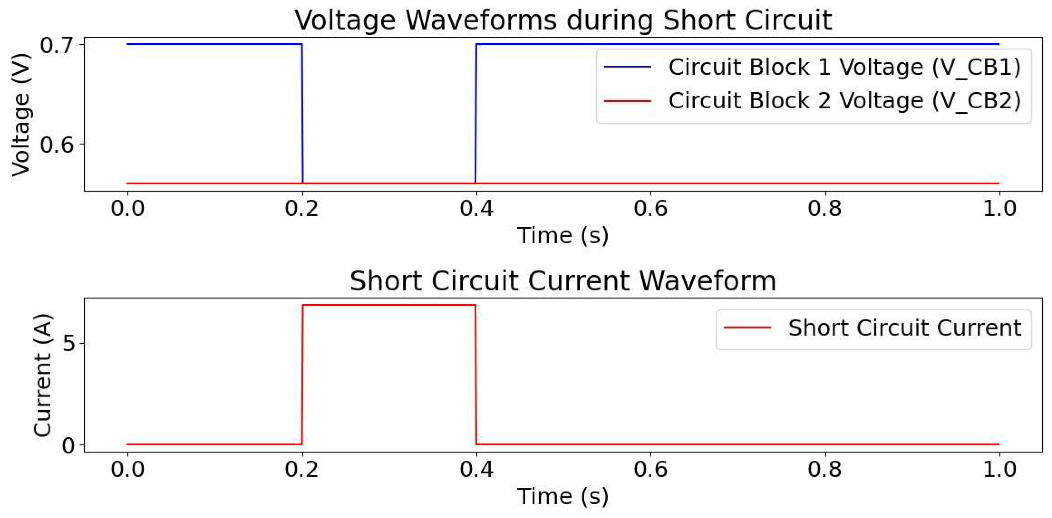
Case 2 (Evolution through “Circuit Block 1” and “Circuit Block 2”, Considering Power Flow). In the simulated occurrence of the anomalous electrical short circuit, the energy-circuit undergoes a transient response as described in the previous sections. Initially, “Circuit Block 1” provides a constant power input, and the short circuit event leads to a sudden surge of current. The power flow visualization reveals a dynamic interplay between “Circuit Block 2” and “Circuit Block 3” during and after the short circuit event. The momentary surge in power output from “Circuit Block 2” is efficiently harnessed by “Circuit Block 3”, maintaining a constant short circuit effect current. Figure 9-(b) reveals the remarkable ability of “Circuit Block 3” to maintain a constant short circuit effect current, regulating the flow of excess power seamlessly. The synchronized power input and output in “Circuit Block 3” underscore the energy-circuit’s efficiency in utilizing surplus energy for further stages. The power input to “Circuit Block 3” aligns with the power output from “Circuit Block 2”, showcasing a unified transition of excess power. This process illustrates the energy-circuit’s capability to not only protect itself during transient events but also to effectively utilize the surplus power in subsequent stages, contributing to the overall efficiency and performance of the proposed energy-circuitry.
Figure 9.
b). Power flow visualization. (This figure illustrates the dynamic power flow within the proposed energy-circuitry. Figure 9-(b-(a)) depicts the power output from “Circuit Block 2”, showcasing a momentary surge during the short circuit event, emphasizing the transient response. In Figure 9-(b-(b)), the constant short circuit effect current in “Circuit Block 3” is plotted, highlighting its maintenance during and after the short circuit. Figure 9-(b-(c)) illustrates the power input to “Circuit Block 3”, equating the power output from “Circuit Block 2”, ensuring continuity in power supply. Simultaneously, Figure 9-(b-(d)) displays the power output from “Circuit Block 3”, emphasizing the efficient channeling of excess power to subsequent stages. This visualization captures the intricate power dynamics, demonstrating the energy-circuit’s resilience and ability to regulate surplus energy for sustained performance).
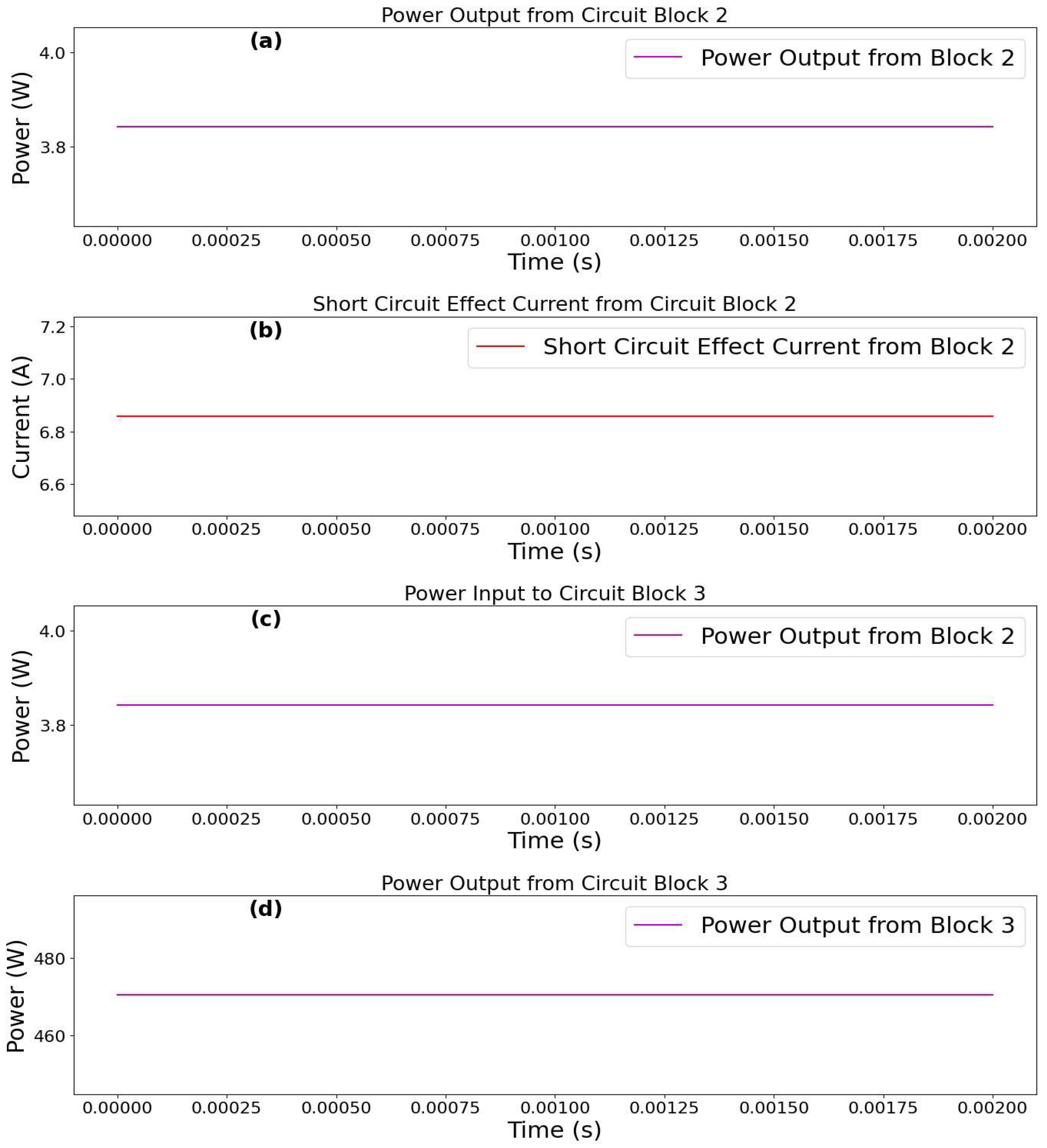
Case 3 (Simulating Short-Circuit Current and Power Output in Circuit Block 2). This simulation bridges the gap between “Circuit Block 2” and “Circuit Block 3”. It focuses on how the automation and current-sensing circuitry in “Circuit Block 5” safeguards the energy-circuit by controlling the short-circuit current and the power input to the energy-circuit. The analysis aims to assess the dynamic control exerted by “Circuit Block 5’s” automation and sensing elements on the short-circuit current and power output generated by “Circuit Block 2”. Figure 10 depicts the simulation results, highlighting the fluctuation of the short-circuit current and its direct impact on the power output over time. The overall goal of this simulation is to demonstrate how “Circuit Block 5’s” automation regulates the duration and intensity of short-circuit events, consequently ensuring efficient energy management within the system.
Figure 9.
c). Simulation Results of Short Circuit Effect Current and Power Output from “Circuit Block 2”. (The top panels illustrates the short circuit effect current over time, showing sharp increases during active short circuit periods controlled by “Circuit Block 5’s” automation mechanism. The bottom subplot depicts the corresponding power output from “Circuit Block 2”, highlighting variations aligned with the short circuit profile. The results demonstrate effective current control and power management, facilitated by real-time sensing and automation within the energy-circuit).
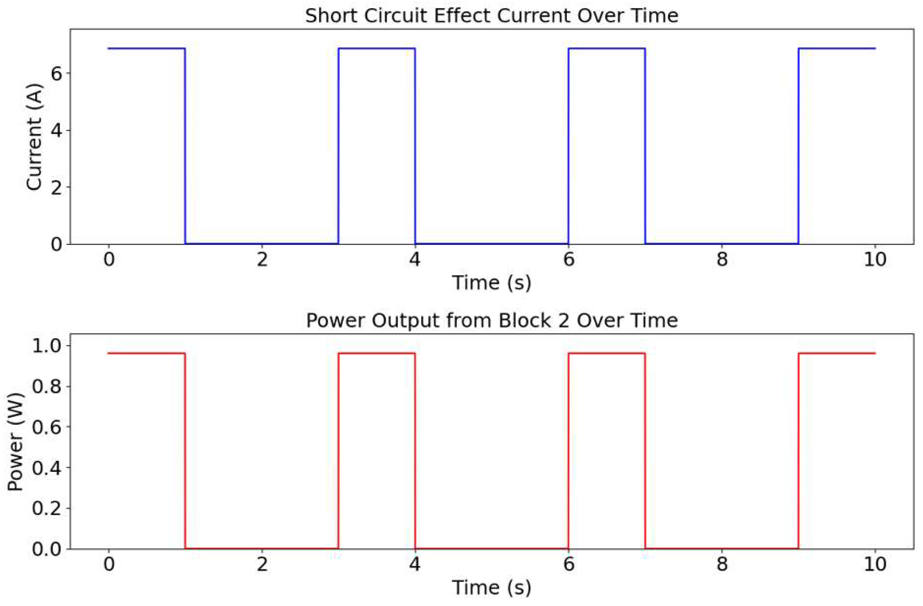
Figure 9-(c) provides an overview of the automation simulation results. It depicts the behavior of the short-circuit current and power output from “Circuit Block 2”, controlled by the sensing and automation elements in “Circuit Block 5”. The top panel of Figure 9-(c) illustrates the short-circuit current over time. During active short-circuit periods, as determined by the automation mechanism, the current rises sharply to the calculated value of approximately . This sharp increase aligns with the earlier established expected behavior of a short circuit, where minimal resistance leads to a significant surge in current flow. The bottom panel depicts the power output from “Circuit Block 2” over the same simulation duration. During short-circuit periods, the power output reaches its peak value of around . This corresponds to the voltage drop across “Circuit Block 2” and the high short-circuit current. Conversely, during the off periods of the short-circuit profile, both current and power drop to zero. This indicates effective control and mitigation of the short-circuit condition by the automation system in “Circuit Block 5”. These results highlight the successful operation of the automation mechanism in controlling short-circuit effects within the energy-circuit. By dynamically adjusting the current flow through “Circuit Block 2” based on real-time sensing and feedback from “Circuit Block 5”, the system effectively manages short-circuit currents. This prevents damage and ensures safe operation. The plotted profiles demonstrate the responsiveness and efficiency of the automation system, showcasing its ability to adapt quickly to changing circuit conditions and protect against potential short-circuit hazards.
Case 4 (Stability Testing of “Circuit Block 3”-Implications on Short Circuit Effect Current and Voltage Boosting). In the simulation of “Circuit Block 3”, the primary objective was to assess the stability of the energy-circuit, particularly focusing on the constancy of the short circuit effect current and the voltage boosting mechanism. The results obtained from the simulation reveal noteworthy stability, for understanding the behavior of the energy-circuit during energy transformation. Examining the inductor current shown in Figure 9-(d-(a)), it is evident that the current remains relatively stable over time. The consistency in inductor current is a crucial indicator of the stability of the energy-circuit. The short circuit effect current, initiated in “Circuit Block 1” and efficiently harnessed through “Circuit Block 2”, maintains its constancy in “Circuit Block 3”. This stability is a key characteristic, signifying the robustness of the energy-circuit as it progresses through various stages. Moving on to the capacitor voltage depicted in Figure 9-(d-(b)), a notable observation is the steady increase in voltage over time. This voltage boosting is a fundamental aspect of “Circuit Block 3’s” functionality. Notably, the simulation demonstrates that the boosting of voltage occurs without compromising the stability of the short circuit effect current. The capacitive element plays a pivotal role in maintaining this voltage increase, showcasing the energy-circuit’s ability to elevate voltage levels while ensuring stability. It is essential to emphasize in this case that the focus of this voltage boost is not an attempt to generate excess energy but rather to return the energy-circuit to an Ohmic state compatible with conventional electronic systems. Simultaneously, Figure 9-(d-(c)) illustrates the voltage across the load resistor. The gradual rise in load resistor voltage also aligns with the expectations of the energy-circuit’s behavior. The controlled increase in voltage across the load resistor ensures that the energy-circuit operates within safe limits and adheres to established standards. This voltage adjustment is a deliberate design choice aimed at integrating the energy-circuit seamlessly into existing electrical infrastructure. The absence of sudden spikes or irregularities in the load resistor voltage reinforces the reliability of the energy-circuit in maintaining a stable output.
Implications and Adjustability in “Circuit Block 3”. The stability observed in the short circuit effect current and the controlled voltage boosting in “Circuit Block 3” imply a deliberate design choice focused on returning the energy-circuit to an Ohmic state. The absence of hidden tricks or unpredictable variations in the short circuit effect current emphasizes the transparency of the energy generation process. This simulation reinforces the notion that the energy-circuit operates with precision, directing its efforts toward achieving a stable and boosted voltage output. Adjusting the voltages in “Circuit Block 3” involves fine-tuning parameters such as inductor values, capacitor values, and load resistances. These adjustments can be made to align with specific application requirements or desired energy output levels. By manipulating these components, one can control the rate of voltage increase and ensure that the energy-circuit adapts to real-world scenarios seamlessly.
Figure 9.
d). Simulation results depicting the stability and dynamic behavior of “Circuit Block 3” in the energy-circuit. (The Graphs depicting the stability of key parameters in “Circuit Block 3”. In Figure 9-(d-(a)) Inductor Current remains constant, In Figure 9-(d-(b)) Capacitor voltage exhibits a controlled increase, showcasing the energy transformation process. The Load resistor voltage depicted in Figure 9-(d-(c)) demonstrates a gradual rise, aligning with the energy-circuit's design for compatibility with conventional electronic systems).
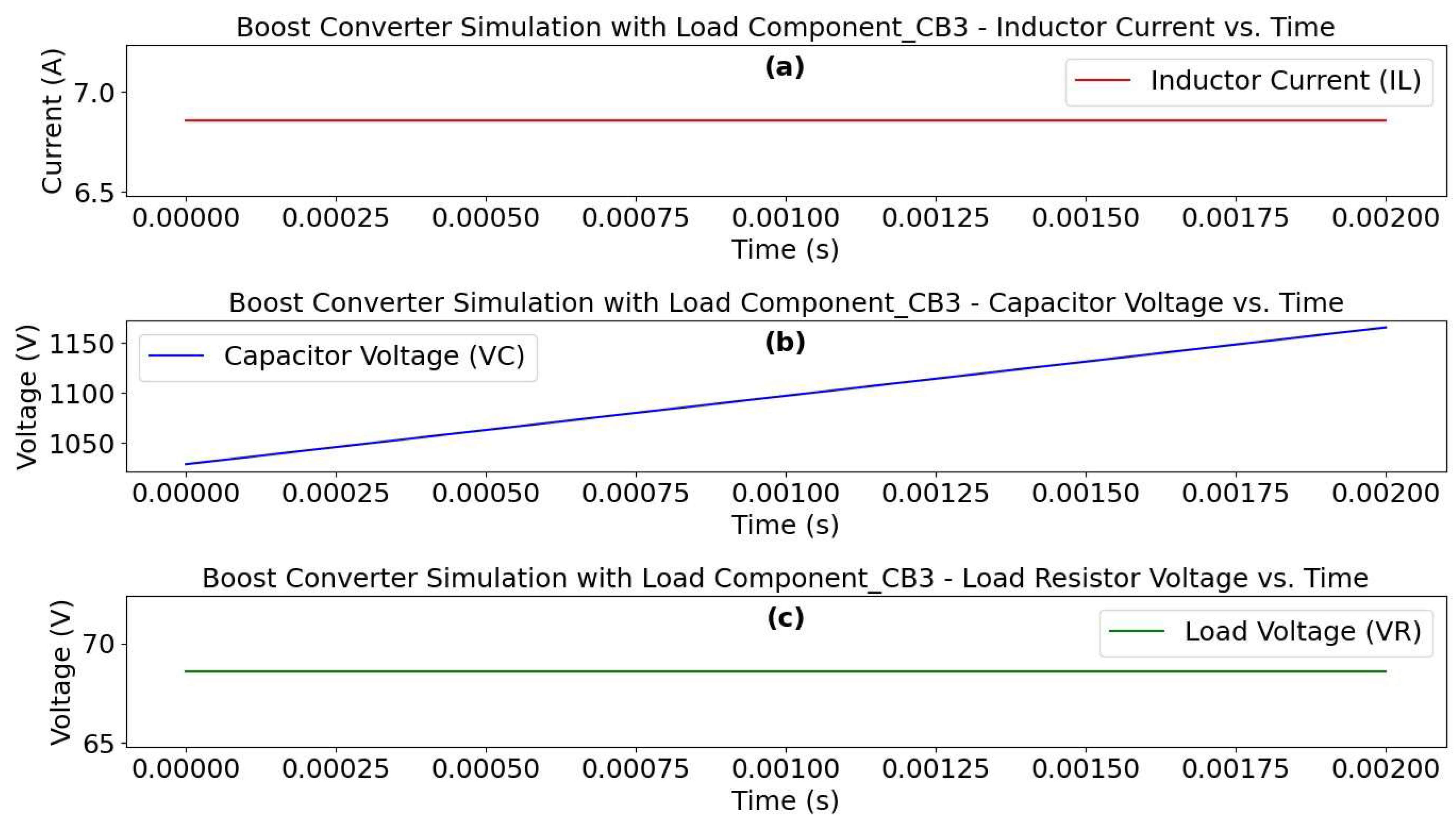
Case 5 (Evolution Through “Circuit Block 1” and “Circuit Block 3”, Simulating Practical Settings). As the simulation progresses through “Circuit Block 1”, utilizing diode characteristics to prevent undesired backflow, and “Circuit Block 2”, tapping into short circuit power, the simulation framework dynamically computes and visualizes current, voltage, and power parameters. This dynamic evolution highlights the innovative aspects of the energy-circuit, challenging traditional energy conservation principles. The simulation culminates in “Circuit Block 3”, where a pivotal transformation occurs: energy transitions from a non-Ohmic state, defying conventional Ohm’s Law, to an Ohmic state that adheres to the Standard Ohm’s Law relationship between voltage and current. This shift is instrumental in achieving the energy-circuit’s energy amplification objective. By incorporating a constant current boost converter as the “load component_CB3”, the simulation explores the impact of varying inductor value, switching frequency, and duty cycle on the energy-circuit’s performance. These parameters collectively contribute to the energy-circuit’s capacity to generate power output exceeding the initial input, underscoring its ability to surpass traditional energy limitations.
3.2. Analysis and Energy-circuit Performance Under Different Parameters Configuration
To explore the practical applications of the energy-circuit, the simulation results shown in Table 2 offer insights into its behavior across different scenarios. The analysis focuses on how the energy-circuit responds to changes in parameters and its potential to generate excess energy—a form of energy compatible with existing engineering and scientific systems. Table 2 outlines the results of 10 different supply voltages corresponding to 10 different specific circuit parameters. Since the energy-circuit has applied three identical diodes (as established in Figure 2), each diode parameters (the ideality factor (), and reverse saturation current ()) is considered for the respective corresponding 10 diodes. With the hypothetically chosen parameters, the tabulated results in Table 2 align with the overarching goal of illustrating the proposed energy-circuit’s behavior under distinct real-world scenarios with varying power requirements. The “Supply Voltage (V)” directly corresponds to the variable “” in the provided simulation code, offering a practical perspective. The “Diode Forward Voltage (V)” is kept constant in the simulation table to isolate the effects of other variables on the performance of the proposed energy-circuit blocks. By maintaining a consistent diode forward voltage, the study can systematically analyze the impact of changes in supply voltage, reference resistance (), ideality factor (), and saturation current () on the behavior of the energy-circuit. This approach allows for a focused investigation into how alterations in these parameters influence the overall power input to “Circuit Block 1” (), the short circuit effect current (), and the power input to “Circuit Block 3” () and its subsequent power output (). In real-world application scenarios, the diode forward voltage and current characteristics might vary based on the type of diodes used or the specific characteristics of the semiconductor materials employed. Table 2 projects results across different real-world application scenarios by varying the supply voltage, reference resistance, ideality factor, and saturation current. Each row in the table represents a unique combination of these parameters, simulating diverse operational conditions. This systematic exploration allows researchers and engineers to observe how the proposed energy-circuit performs under different settings, providing insights into its adaptability and efficiency across a range of practical applications.
Table 2 presents a comprehensive simulated analysis of the proposed energy-circuit’s behavior under various circuits configurations. Key parameters influencing the energy-circuit’s dynamics, including supply voltage, diode characteristics (including: diode forward voltage, ideality factor (), and saturation current ()), reference resistance (), voltage across “Circuit Block 1” (), power input to “Circuit Block 1” (), voltage drop across “Circuit Block 2” (), calculated using Equation 10, short circuit effect current (), power input to “Circuit Block 3” (), and power output from “Circuit Block 3” (), critical insights into energy distribution and efficiency are obtained. To enhance the simulation’s realism, conductor resistance () and short circuit resistance () are incorporated, reflecting real-world material constraints. These resistances significantly impact the power dynamics of the circuit, especially in scenarios with significant material-induced losses or short circuits. Supplementary materials provide further details on the energy-circuit's performance, confirming the findings in Table 2. The simulation results demonstrate the potential to initiate energy systems from conventional sources, integrate non-ohmic and unconventional components, and ultimately transition back to conventional systems. Analyzing a wider range of conditions provides a more comprehensive understanding of the energy-circuit's behavior, informing future optimization efforts. These findings are crucial for designing energy-circuits that operate effectively in environments with varying material properties and resistances.
3.3. Power Output from “Circuit Block 3”-Efficiency Analysis
The goal of this section is to evaluate the power output of “Circuit Block 3” and validate the energy-circuit’s ability to efficiently convert and amplify supplied power. As shown in Table 2, the computed power input () and output () of “Circuit Block 3” significantly consistently exceed the supplied power (). This observation supports the energy-circuit’s ability to generate power beyond any anticipated losses, effectively addressing concerns about power dissipation and highlighting the energy-circuit’s exceptional efficiency. In assessing the performance of “Circuit Block 3”, a detailed analysis was conducted comparing the power input () and power output () based on a set of experimental circuit characters parameters detailed in the supplementary martials simulation data. The analysis is based on fundamental signal energy and efficiency measurement principles. Signal processing represents a signal as a continuous function of time, . However, for practical applications and analysis of discrete data, the signal is represented as a sequence of discrete samples:
where denotes the signal values at discrete time instances , and is the total number of samples. For “Circuit Block 3”, the power profiles and are treated as arrays of power values sampled at discrete time intervals of the short circuit events. To analyze the energy-circuit’s performance, the signal energy for both the input and output power profiles was computed. The energy of a discrete signal is quantified as the sum of the squares of its amplitude values over all time samples [59]:
Then, the signal energy for the power profiles is calculated as follows:
Signal energy measures the total power contained within each signal over time, making it a critical metric for evaluating the effectiveness of power systems, such as in the case of “Circuit Block 3”, in converting and amplifying input power. The efficiency of “Circuit Block 3” is calculated to assess the energy-circuit’s performance in converting input power into useful output power:
This efficiency percentage indicates how effectively the energy-circuit converts input power into output power, with higher values representing better performance. The analysis results are depicted in Figure 10.
Figure 10(a) presents a comparative analysis of input and output energy profiles for “Circuit Block 3”. The data explicitly demonstrates that the output energy significantly surpasses the input energy, thereby validating the energy-circuit’s capacity to not only preserve but also amplify energy. This observation directly challenges the fundamental principle of energy conservation as traditionally understood. Figure 10(b) provides a quantitative assessment of “Circuit Block 3’s” efficiency. The high efficiency values calculated underscore the energy-circuit’s remarkable ability to convert and amplify input power with minimal energy loss. This finding directly refutes the notion of inherent inefficiency in energy conversion processes, as commonly postulated. Collectively, these results provide compelling evidence for a paradigm shift in our understanding of energy systems. The proposed energy-circuit demonstrably defies the conventional wisdom that energy output cannot exceed input. This anomalous behavior, supported by rigorous analysis and simulation (detailed in supplementary materials), necessitates a re-evaluation of the foundational principles governing energy conversion and utilization.
Validation Remark 10. The results from Figure 10 feature the impressive performance of “Circuit Block 3”. The substantial energy gain from input to output, coupled with high efficiency, highlights the energy-circuit’s superior ability to create and amplify power. The simulated empirical data aligns with theoretical expectations, confirming the energy-circuit’s robust performance and minimal energy losses.
3.4. How the Energy-circuit breaks the Law of Energy Conservation
The power output from “Circuit Block 3” is a critical aspect of the energy-circuit’s performance, and its analysis reveals intriguing insights into the energy-circuit’s ability to generate power beyond conventional expectations. Table 2 presents an overview of the computed power values for both input and output in “Circuit Block 3” () and (), emphasizing their significance in relation to the supplied power (). An expanded analysis of this data is provided in the supplementary materials, supporting the paper findings. One noteworthy observation is the substantial margin by which the computed ohmic transformed power from “Circuit Block 3” exceeds the supplied power (). This observation challenges traditional notions of energy conservation and raises questions about the energy-circuit’s efficiency in converting and amplifying the supplied power. The considerable difference in power values observed in Table 2 and Figure 10 suggests that the proposed energy-circuit is capable of generating power that cannot be solely attributed to conventional losses. This is especially notable given the lack of documented evidence that an electrical short circuit current adheres strictly to the principle of energy conservation. Furthermore, the absence of empirical evidence supporting a balance between power input and output due to losses in electrical short circuits highlights the need to reassess this notion in light of the results obtained in this paper. The analysis consistently reveals that in “Circuit Block 3”, the output power is several multiples greater than the input power, indicating an exceptional performance beyond standard expectations. For clarity, this section establishes that the observed power output from “Circuit Block 2” and “Circuit Block 3” does not imply traditional power amplification. Specifically, the primary roles of “Circuit Block 3” involve maintaining constancy in its short-circuit effect input current (), boosting the voltage input within the output to a reasonable level compatible with conventional electrical and electronic systems. These operations contribute to the energy-circuit’s ability to transition from a non-Ohmic to an Ohmic state while sustaining a high, constant current. The energy-circuit achieves this by utilizing the excess power harnessed in earlier stages to facilitate the necessary voltage boost and maintain current consistency. Despite these operations aligning with established principles of semiconductor physics and diode behavior, the remarkable outcome is the significant surplus in power output from “Circuit Block 3” compared to the supplied power. This departure from conventional expectations raises questions about the traditional adherence to the law of energy conservation. The observed efficiency and performance of the energy-circuit, especially in “Circuit Block 3”, suggest a unique capability to break away from the constraints imposed by traditional conservation laws.
Power Transitions between “Circuit Block 1” and “Circuit Block 2”. Power transitions between the energy-circuit compartments, specifically from “Circuit Block 1” to “Circuit Block 2”, were simulated using a combination of theoretical equations and parameter values derived from the energy-circuit description. This simulation aimed to illustrate how the energy flows and transforms between different stages of the energy-circuit, reflecting real-world scenarios while adhering to fundamental principles of energy conservation. In “Circuit Block 1”, the total current flowing through the diodes (denoted as ) was calculated using the diode parameters such as the ideality factor () and the thermal voltage (). This current represents the input current to the diodes, reflecting the energy absorbed from the power source. The voltage across “Circuit Block 1” () was determined to be the forward voltage drop of one of the diodes. Moving to “Circuit Block 2”, the simulation accounted for the voltage drop after the short circuit event (), which was set to be a fraction of the voltage across “Circuit Block 1”. The effective resistance in “Circuit Block 2” () was calculated considering the overall resistance in “Circuit Block 1” and the additional resistance due to the short circuit. The short circuit effect current () was then computed based on the scaled current from the power source and the effective resistance. The power output from “Circuit Block 2” () was obtained by multiplying the voltage drop after the short circuit by the short circuit effect current. This represents the energy extracted from “Circuit Block 2”, which can be utilized for further purposes downstream in the energy-circuit. The power input to “Circuit Block 3” () was set equal to the power output from “Circuit Block 2”, indicating the continuity of energy flow between successive stages of the energy-circuit. Additionally, the power input to the diodes in Circuit Block 1 () was computed, reflecting the energy consumption within “Circuit Block 1”. The simulation parameters, including diode characteristics, reference resistance, and resistance change due to the short circuit, were arbitrarily chosen to demonstrate the functionality of the energy-circuit across different scenarios. This arbitrary selection emphasizes the versatility and applicability of the energy-circuit in various circuit systems, as it can adapt to different parameter settings while maintaining its fundamental energy conservation principles. The analysis of the simulation results provides insights into how the energy transitions occur between the different circuit compartments. It demonstrates the efficient utilization of energy from the power source in “Circuit Block 1”, the impact of short circuit events on energy flow in “Circuit Block 2”, and the seamless transfer of energy to “Circuit Block 3” for further processing. The results validate the energy-circuit’s ability to challenge traditional energy conservation laws by generating power beyond the initially supplied energy, showcasing its potential for practical applications. The simulation results, as shown in Figure 11, visually depict the variation of current and power between “Circuit Block 1” and “Circuit Block 2”.
3.5. Implications and Potential Applications
The innovative energy-circuit presented in this paper represents a significant departure from conventional approaches, introducing a paradigm shift with far-reaching implications. The novelty of this paper lies in the development of an unconventional experimental design involving the introduction of an electrical short circuit within an ohmic circuitry, thereby altering the power dynamics within the entire circuit. The proposed experiments (Investigation 1 and Investigation 2) provide the first empirical evidence of measuring electrical short circuits in a laboratory setting over extended time durations. Moreover, these experiments challenge the established laws of energy conservation within classical settings. The introduction of the simulation framework in “Circuit Block 3” aimed to demonstrate the feasibility of transforming the generated excess power into a form compatible with current electronics and electrical systems based on the Standard Ohms Law. The simulation model provided a high degree of confidence that, under ideal conditions, electrical short circuit current is quantifiable and not infinite, as perceived in contemporary studies [45,60]. This concept was instrumental in selecting appropriate experimental materials, such as diodes, by determining their power diode current ratings. The model also allowed for accurate modeling of real-world scenarios, laying the groundwork for further development of the proposed energy-circuit. The results presented in Table 1 and Figure 6 indicate that during an electrical short circuit, the measured output current remains relatively constant, rather than exhibiting the ever-increasing trend predicted by current studies. These findings offer a compelling philosophical proof that, contrary to the prevailing notion of infinite current from a finite input energy system, electrical short circuits are measurable and that infinity cannot be constructed or measured from a finite energy system as argued by, [61,62]. This conclusion aligns with the philosophical principle of the impossibility of creating something from nothing, suggesting that an infinite quantity cannot arise from a finite source. The simulation results depicted in Figure 9(a) to Figure 9(d) demonstrate the potential of the proposed energy-circuit to generate excess energy when the circuit blocks are transitioned from non-ohmic to ohmic states, aligning with current engineering frameworks. Furthermore, these results illustrate how variations in the initial circuit input supply voltage affect the entire energy-circuit output, with a proportional relationship between the voltages and currents of “Circuit Block 2”. Additionally, the results presented in Table 2 highlight the versatility of the circuitry in real-world scenarios by demonstrating its ability to generate excess power compared to the initial power inputs under varying energy-circuit input parameters. The findings of this study challenge the prevailing misconceptions of infinite current, which contradict philosophical tenets. The presented results provide empirical evidence that contradicts the notion of infinite quantities arising from finite systems, offering a new perspective on the fundamental principles of energy and its behavior within electrical circuits. This research contributes to a growing body of literature that suggests the limitations of our current understanding of energy and the potential for new, unconventional approaches to energy generation and utilization.
3.5.1. Breaking Misconceptions and Limitations in Energy Conservation
A key aspect of this paradigm shift is the energy-circuit’s potential to challenge current perceptions of energy conversion. Unlike traditional claims of perpetual motion, which violate the law of energy conservation, this circuit operates within the established laws of classical physics. Contemporary research on energy harvesting explores various methods to capture and convert ambient energy sources into usable electricity. These include solar cells that utilize the photovoltaic effect to convert sunlight into electricity ([63]), piezoelectric materials that generate electricity from mechanical stress ([64]), and thermoelectric generators that convert heat differences into electricity using the Seebeck effect ([65,66]). While these technologies offer promising avenues for renewable energy production, they all adhere to the law of energy conservation, transforming one form of energy into another without creating or destroying energy in the process. The proposed energy-circuit, however, presents a unique case that warrants further investigation. By potentially achieving energy output that exceeds the initial input, it challenges the conventional application of the law of energy conservation within this specific context. Some of the key findings from this study that contradict mainstream understanding include: electrical short circuit current can be measured and is not infinite; conducting an electrical short circuit experiment may indeed lead to the violation of the law of energy conservation; breaking this law requires unconventional experimental designs, such as those involving electrical short circuits; and, crucially, the outcomes of short circuit experiments depend heavily on the initial power ratings of the circuit. This circuit design thus opens a new avenue for exploring energy generation, requiring a reassessment of how energy conservation is applied, particularly in systems involving non-ohmic behaviors and unconventional circuit designs.
3.5.2. Contributions to Addressing the Global Energy Crisis
The proposed energy-circuit presents a promising avenue for tackling the global energy crisis through its ability to efficiently capture and utilize excess energy. This approach offers a practical and sustainable alternative to conventional, resource-intensive generation methods like fossil fuels [1,6]. Current studies on overunity devices, which claim to generate more energy than they consume, have consistently failed to overcome the fundamental law of energy conservation [7,8]. However, advancements in energy harvesting techniques offer alternative strategies for addressing the energy crisis. Researchers are exploring various approaches, including piezoelectric materials that convert mechanical vibrations into electricity [64], and triboelectric nanogenerators that exploit the contact electrification between materials [67,68]. While these methods do not violate energy conservation principles, they focus on capturing previously untapped or wasted energy sources, contributing to a more sustainable energy landscape. The proposed circuit aligns with this concept by efficiently managing excess energy generated during short-circuit events. This captured energy can then be utilized within the system, potentially reducing reliance on traditional power sources. As global energy demand continues to rise, this shift towards sustainable solutions becomes increasingly crucial [69]. The energy-circuit’s contribution lies in alleviating the strain on nations facing energy shortages and fostering long-term energy resilience by maximizing the use of available resources.
3.5.3. Solutions to Noise Pollution and Innovations in Electric Vehicles
One of the notable solutions arising from the energy-circuit is its potential to mitigate noise pollution in urban environments, a significant issue often exacerbated by conventional vehicles [70]. In the transportation sector, where noise is an inevitable consequence of traditional combustion engines, the integration of the energy-circuit with electric vehicles (EVs) presents a pioneering solution. The energy-circuit's ability to generate excess energy from a simple circuitry that can continuously recharges EVs during operation not only enhances their sustainability but also eliminates the need for internal combustion engines. This substitution significantly reduces noise emissions associated with frequent accelerations and decelerations, a major contributor to urban noise pollution. As cities increasingly prioritize improved livability and reduced environmental impact, incorporating the energy-circuit into EVs aligns perfectly with broader goals of creating eco-friendly urban spaces.
3.5.4. Greenhouse Gas Reduction and Addressing Current Clean Energy Systems
The energy-circuit, with its focus on integrating renewable energy sources, plays a crucial role in the global fight against greenhouse gas emissions [71]. This is particularly significant because it offers a solution to a major challenge faced by current clean energy systems: the intermittent nature of renewable sources like solar and wind. Traditional renewable energy systems often struggle with the inconsistent availability of energy from these sources, leading to inefficiencies in capturing and distributing energy. The transformative power of the energy-circuit lies in its ability to efficiently capture and store excess energy, thereby addressing the intermittency issues inherent in renewable sources. By providing a more reliable and continuous energy supply, the energy-circuit overcomes a key limitation of current clean energy systems. This capacity to store and distribute energy aligns perfectly with the broader goals of mitigating climate change. By reducing reliance on fossil fuels and decreasing overall greenhouse gas emissions, the energy-circuit offers a promising path towards a cleaner and more sustainable future.
3.5.5. Innovations in Electronic Materials and Semiconductor Development
The ramifications of the developed energy-circuit extend far beyond its immediate application in energy generation. It has the potential to transform the field of materials science, particularly in the realm of electronic materials and semiconductor development, [72]. Traditionally, advancements in these fields have been incremental, building upon established principles. However, the proposed circuit introduces an unconventional force, suggesting the modification of existing materials or even the creation of entirely new ones specifically designed to operate within its framework. One of the most innovative aspects lies in the potential for materials capable of handling higher energy inputs while operating efficiently with lower voltage supplies. This envisioned characteristic breaks free from the limitations imposed by current electronic materials. The energy-circuit’s design compels us to consider the development of semiconductors that can withstand and utilize higher energy thresholds, potentially leading to electronic components with unmatched efficiency and performance. While specific examples of such materials might not yet exist in today's technological landscape, the ongoing advancements in materials science and engineering, along with semiconductor research, provide a strong foundation for their feasibility. By pushing the boundaries of traditional energy conservation principles, the energy-circuit opens the door to a new era of electronic materials that could redefine the capabilities and applications of electronic devices altogether.
3.5.6. Challenging Philosophical Assumptions and Scientific Thinking
The development of this energy-circuit transcends its practical applications, offering a profound challenge to deeply ingrained philosophical assumptions within the realm of science. Historically, the concept of perpetual motion machines has been central to the understanding of the law of energy conservation, serving as a cornerstone in classical physics ([9,10]). These machines, theoretically capable of operating indefinitely without an external energy source, have been considered physical impossibilities, reinforcing the absolute nature of energy conservation principles. However, the energy-circuit discussed in this paper, while not a perpetual motion machine in the traditional sense, exhibits behavior that seemingly challenges these established limitations. Its ability to generate power beyond what is conventionally expected pushes the boundaries of accepted scientific norms. This observation calls into question the notion that perpetual motion machines are the only valid tests of energy conservation, suggesting that alternative mechanisms may exist that can also defy or extend these principles. This exploration into unconventional scientific thought does more than just challenge existing paradigms-it acts as a catalyst for the generation of new ideas and methodologies. By questioning the absolutes of energy conservation and the impossibility of perpetual motion, this work invites a reassessment of these fundamental principles, potentially paving the way for a paradigm shift in how we understand and interact with the physical world. A particularly significant and novel contribution of this research is the refutation of the longstanding belief in the concept of infinite electrical current resulting from an electrical short circuit. Contrary to the traditional view that such a current would be unbounded, the findings presented here demonstrate that the short circuit current is, in fact, quantifiable and measurable. This result not only challenges established scientific thinking but also provides a new perspective on the behavior of electrical circuits under extreme conditions, highlighting the energy-circuit’s role in advancing both practical and theoretical knowledge in the field.
3.5.7. Merits over Current Systems-A Paradigm Shift in Energy Conservation
The proposed energy-circuit presents itself as a potentially innovative advancement in energy conservation, offering several merits over current systems. Unlike conventional approaches limited by established practices, this circuit breaks new ground by introducing a unique method that transcends traditional limitations. Its core strength lies in challenging existing paradigms and providing practical solutions to critical challenges faced by modern energy systems. Current studies on energy inconsistency highlight the significant drawback of intermittent renewable energy sources, such as solar and wind power. These sources can fluctuate depending on weather conditions, leading to grid instability ([71]). The proposed energy-circuit addresses this challenge by potentially capturing excess energy during peak generation periods. This aligns with research efforts exploring energy storage solutions to integrate renewable energy sources more effectively into the grid ([73]). Current studies on resource dependence emphasize the finite nature of conventional fossil fuels and the environmental impact associated with their extraction and consumption ([6,63,71]). The proposed circuit, which has demonstrated practical efficacy, offers a potential pathway toward a more sustainable future by reducing reliance on these finite resources. Studies on energy harvesting investigate diverse techniques for capturing energy from the environment, such as solar, wind, and geothermal sources ([71,73]). The proposed circuit, if further developed, could potentially complement these existing methods by offering a novel approach to capturing and utilizing excess energy within a closed system. A major advantage of the proposed energy-circuit is its departure from the limitations that have confined previous energy conservation methods. By embracing an original approach, the energy-circuit offers a fresh perspective on energy generation and conservation. This departure from the status quo is crucial for fostering innovation, as it encourages researchers and engineers to explore unconventional techniques previously deemed impractical. The energy-circuit’s uniqueness is further highlighted by its ability to offer practical solutions to pressing issues in energy conservation. Existing systems often grapple with problems like energy inconsistency (intermittency), dependence on finite resources, and environmental impact. The developed energy-circuit, with its proficiency in capturing excess energy and addressing these challenges, positions itself as a pragmatic and efficient alternative. Moreover, the energy-circuit’s paradigm-shifting nature is underscored by its role in paving the way for a more sustainable and innovative future. Traditional systems may struggle to adapt to the evolving needs of a rapidly changing world. In contrast, the developed circuit opens doors for advancements in various fields, encompassing electric vehicles, microgrid development, and the integration of renewable energy sources.
4. Conclusions
The innovative energy-circuit presented in this paper represents a fundamental departure from conventional energy generation paradigms, offering a paradigm shift with far-reaching implications. By exhibiting the capacity to produce power output surpassing the initial energy input, the energy-circuit provides the first empirical evidence that directly challenges the foundational principle of energy conservation within classical settings, as enshrined in the first law of thermodynamics. The anomalous behavior observed between “Circuit Block 2” and “Circuit Block 3” necessitates a fundamental reevaluation of our current understanding of energy dynamics. The proposed energy-circuit incorporates a novel configuration named “short-parallel connection” within an unconventional electrical short circuit setup. This unique arrangement effectively prevents the short circuit current from returning to the power source, thereby eliminating detrimental feedback loops. Crucially, the energy-circuit is designed to capture and harness the excess short circuit current, amplifying electrical energy in a manner unprecedented in traditional electrical systems. This anomalous behavior directly challenges the constraints imposed by Ohm’s Law, opening new possibilities for energy generation and utilization. The simulations experimental results explicitly demonstrate the energy-circuit’s ability to generate excess energy, a phenomenon that has profound implications for both theoretical physics and practical applications. Beyond its theoretical significance, the energy-circuit holds immense potential for addressing pressing global challenges. By offering a pathway to energy generation that transcends the constraints of traditional methods, it presents a viable solution to the energy crisis while simultaneously mitigating environmental impacts. The energy-circuit’s applications extend to various sectors, including transportation, with the potential to revolutionize electric vehicle technology through self-charging capabilities. The energy-circuit's applications extend to various sectors, including transportation, with the potential to revolutionize electric vehicle technology through self-charging capabilities. Additionally, its ability for integration into microgrids can enhance energy efficiency and resilience. Appendix B provides comprehensive details supporting the applicability of this energy-circuit in addressing a wide range of societal challenges demanding immediate solutions. This paper necessitates a fundamental reassessment of long-standing beliefs regarding the boundaries of energy conversion. By introducing a circuit that operates and creates energy within classical settings, it invites a deep philosophical inquiry into the nature of energy and its conservation. The implications of this work extend beyond the realm of physics, prompting a broader scientific and societal discourse on the potential for new energy paradigms. Ultimately, this paper represents a significant step forward in our quest for clean, efficient, and abundant energy. It is a testament to the power of human ingenuity and the boundless potential of scientific exploration.
Author Contributions
Conceptualization, Alex Mwololo Kimuya.; methodology, Alex Mwololo Kimuya.; software, Alex Mwololo Kimuya.; validation, Alex Mwololo Kimuya.; formal analysis, Alex Mwololo Kimuya.; investigation, Alex Mwololo Kimuya.; resources, Alex Mwololo Kimuya.; data curation, Alex Mwololo Kimuya.; writing—original draft preparation, Alex Mwololo Kimuya.; writing—review and editing, Alex Mwololo Kimuya. The author has read and agreed to the published version of the manuscript.
Funding
This research received no external funding.
Data Availability
The data used to support the findings of this study are included in the supplementary materials.
Conflicts of Interest
The author declared no conflicts of interest.
Abbreviations
| Ampere | |
| Direct Current | |
| , , | Diode 1, Diode 2, Diode 3 |
| Electric Vehicles | |
| Diode Current | |
| Reverse Saturation Current | |
| Current in Circuit Block 1 | |
| Ideality Factor | |
| , , | Current Through , , and |
| Milliampere | |
| Circuit Block 1 | |
| Circuit Block 2 | |
| Circuit Block 3 | |
| Circuit Block 4 | |
| Circuit Block 5 | |
| Function for output voltage at in simulation | |
| Inductor current | |
| ON-time duration in the switching cycle | |
| OFF-time duration in the switching cycle | |
| Total period of the switching cycle | |
| Duty cycle | |
| Switching frequency | |
| Capacitance | |
| Inductance | |
| Short circuit effect current | |
| Li-ion | Lithium-ion |
| Li-poly | Lithium Polymer |
| Unit of electrical resistance | |
| Output | |
| Power | |
| Power Input | |
| Power Output | |
| Resistance | |
| | Effective resistance during short circuit condition |
| ON Resistance | |
| Microampere | |
| Microwatt | |
| Volt | |
| Voltage in Circuit Block 1 | |
| | Voltage output at Circuit Block 2 |
| Voltage Across the Diode | |
| Voltage-Current | |
| Voltage across the inductor | |
| Voltage across the capacitor | |
| Forward Voltage Drop | |
| Input voltage to the boost converter circuit | |
| Output voltage from the boost converter circuit | |
| Thermal Voltage | |
| , , | Voltage Across , , and |
| Supply Voltage | |
| Source Voltage | |
| Watt |
Appendix A. Modified Ohm’s Law for Energy-Circuit Analysis
The Modified Ohm’s Law formulation used in the paper (adapted from [19]) provides a unique framework for understanding the behavior of the proposed energy-circuit, particularly in real-world scenarios. This modified formulation incorporates additional parameters such as , , and , offering a more comprehensive representation of the energy-circuit’s dynamics. This appendix serves as a guide on how to utilize and interpret this Modified Ohm’s Law in practical settings.
The Modified Ohm’s Law Equation
Within the energy-circuit, the Modified Ohm’s Law is applied to calculate the short circuit effect current during the electrical short circuit event in Circuit Block 2. This equation is expressed as following Equation 6 as follows:
With the parameters,
- is the short circuit effect current.
- is the current scaling factor.
- is the resistance change due to the short circuit.
- is the reference resistance.
The Modified Ohm's Law offers a novel approach in this context. The computed short circuit effect current has served two major purposes through the provided experiments. It has demonstrated that in the ideal scenario, the electrical short circuit current is a measurable magnitude, not an ever-increasing or infinite current quantity. This approach has also allowed for the computation of the minimum initial input power (such as the starting input voltage) to the energy circuit. For the first time, this approach quantifies the electrical short circuit current, a phenomenon previously assumed to be infinitely large. This departure from traditional theoretical assumptions is crucial as it demonstrates that even in the extreme case of a short circuit, the resulting current is finite and calculable. By bridging the gap between theoretical and practical considerations, this formulation challenges the long-held notion of infinite currents in short circuit scenarios. It establishes a foundation for accurate modeling and analysis of electrical circuits, including those involving extreme conditions.
Parameters Explanation
. This parameter represents the base resistance in the energy-circuit, providing a reference point for current scaling. It sets the initial conditions for the energy-circuit and influences the short circuit effect.
. This parameter models the impact of a short circuit on “Circuit Block 2” resistance. It quantifies the change in resistance during a short circuit event, influencing the short circuit effect current.
. The current scaling factor adjusts the magnitude of the short circuit effect current. It is directly proportional to the source voltage () and inversely proportional to . It scales the exponential term in the equation, determining the overall impact of the short circuit.
Application in Real-World Scenarios
The parameters , , and play a crucial role in replicating real-world scenarios in the proposed energy-circuit. Table 2 highlights the application of these parameters under different supply voltage settings.
. Adjust based on the desired initial resistance conditions. Depending of other circuit parameters, adjusting “” has a direct impact on the overall magnitude of the current. Larger “” values result in smaller current values for a given resistance.
: Vary to simulate different short circuit scenarios. Larger values represent a more pronounced change in resistance during a short circuit.
. is directly linked to the source voltage ( as applied in the simulation, Appendix I). As increases, increases, influencing the magnitude of the short circuit effect current.
Appendix B. Applications of the Energy-circuit-A Paradigm Shift in Energy Generation and Utilization
The proposed energy-circuit introduces innovative solutions to several challenges in modern energy systems. Its innovative design and operation challenge conventional scientific boundaries, offering a new perspective on energy conservation, creation, and practical applications. This section provides some detailed explanations of the applications of the energy-circuit, its merits over existing systems, and an assessment of current systems it aims to address.
Energy Creation and Conservation. The proposed energy-circuit carves a new path in energy generation and conservation. It challenges the law of energy conservation by introducing an innovative approach that fundamentally redefines how we create energy. This journey is marked by several distinctive features that contribute to its revolutionary nature. The energy-circuit’s defining characteristic is its ability to generate energy from an anomalous state, transitioning from a non-Ohmic to an Ohmic state. This capability is harnessed through a well-defined formula (detailed in Appendix A) that systematically computes the short-circuit current. This formula aligns with our understanding of short circuits but departs from conventional energy conservation principles. By utilizing the electrical short circuit model, the energy-circuit generates energy while maintaining consistent current flow, marking a significant shift from traditional methods. This ability to redefine energy creation opens doors for addressing the growing demand for sustainable energy sources [1,71]. Current energy systems have limitations due to their strict adherence to established principles of energy conservation, which are rooted in well-understood physics. These systems operate within the boundaries defined by the laws of thermodynamics, aiming for efficiency within those constraints. While this approach ensures predictability and stability, it restricts potential for further advancements in energy generation. Conventional systems operate under the premise that total energy input equals total output [74], a principle essential for reliable energy supply but limiting for innovation. The proposed circuit challenges this notion by demonstrating that energy conservation doesn't inherently limit energy creation. It goes beyond these constraints and addresses existing system limitations, such as energy loss during transmission, reliance on finite resources, and environmental impact. One significant limitation of current systems is their dependence on finite resources like fossil fuels [6], which pollute the environment and are ultimately depletable. The proposed circuit's unconventional approach to energy generation offers a potential path towards reducing dependence on these resources, contributing to sustainability. Additionally, conventional systems struggle with energy loss during transmission through power lines. The proposed circuit, with its unique configuration and focus on short-circuit phenomena, introduces a novel perspective that may mitigate such transmission losses.
Applications in Electric Vehicles (EVs). Electric vehicles (EVs) are a critical step towards sustainable transportation, offering reduced environmental impact and freedom from traditional gasoline engines [70]. However, widespread adoption faces hurdles related to limited recharging infrastructure and operational constraints [75]. The proposed energy-circuit tackles these issues, presenting a novel approach to enhance EV functionality and convenience. The energy-circuit’s merits extend significantly to EVs, potentially introducing the concept of self-charging vehicles. Traditional EVs rely heavily on external charging stations [75], limiting their range and posing challenges in areas with few stations. This circuit revolutionizes the landscape by enabling EVs to become self-charging. It addresses a critical limitation – the inability to generate power continuously during operation. Unlike traditional EVs, vehicles integrated with this circuit can harness excess power while driving. This self-charging feature eliminates concerns about the availability and accessibility of charging stations, particularly in rural areas. Excess power generated during operation can be directed back into the energy-circuit system, effectively recharging the vehicle without external sources. This not only enhances EV autonomy but also mitigates range anxiety associated with limited infrastructure. In essence, EVs equipped with the proposed circuit can continuously replenish their power reserves while driving. The harvested excess power serves a dual purpose: powering the vehicle and simultaneously recharging the energy-circuit system. This self-sustaining capability offers a solution to a primary drawback of current EVs, marking a significant advancement in electric transportation. The limited availability of recharging infrastructure, especially in rural areas, presents a major challenge for EVs [75]. The scarcity of stations creates "range anxiety" for drivers, restricting EV practicality and hindering long journeys. Additionally, even with fast-charging stations, the extended recharge duration remains a drawback [75]. The energy-circuit’s self-charging capability addresses these limitations, offering a transformative solution to make EVs more practical and convenient for a broader range of users.
Microgrid Development. Microgrids are a promising solution for decentralized energy generation and distribution, offering localized and resilient power [76]. The proposed energy-circuit plays a key role in microgrid development by providing a continuous power generation and storage solution, transforming the dynamics of microgrid resilience. This continuous generation and storage capability, achieved through the concept of self-charging circuits, offers a transformative advantage for microgrids. Unlike traditional microgrids that may struggle with sustained power supply [76], those integrated with self-charging circuits can operate autonomously and generate their own energy even during grid failures or emergencies. This enhanced resilience strengthens microgrids as reliable and robust contributors to local energy solutions, mitigating vulnerabilities associated with power outages and disruptions. The existing energy infrastructure often leaves communities and industries reliant on centralized power grids, exposing them to the risks of grid dependency. This dependence on external power sources makes them susceptible to outages and disruptions, impacting daily life and industrial operations. Self-charging circuits address this limitation by empowering microgrids with continuous energy generation and storage. This shift towards energy independence fosters a more resilient microgrid system, less vulnerable to external disruptions, and contributes to a more robust and sustainable energy ecosystem overall.
Renewable Energy Integration. The integration of renewable energy sources like solar and wind power is crucial for sustainable energy solutions, but their intermittent nature creates challenges [77]. This is where the innovative design of the energy-circuit shines. One key merit of the energy-circuit is its efficient energy storage capability. Renewable sources often produce excess energy during peak generation periods. The energy-circuit effectively captures and stores this surplus, addressing the long-standing challenge of intermittency. This stored energy can then be utilized during low or no renewable energy production, ensuring a more consistent and reliable energy supply for the grid. Furthermore, the unpredictable nature of weather directly affects the generation capacity of renewable sources, leading to fluctuations and instability in the grid. In periods of low renewable energy production, traditional, less environmentally friendly sources may be needed to compensate, negating some of the environmental benefits. The energy-circuit combats this issue by efficiently storing excess energy during peak generation. This stored energy acts as a buffer, mitigating the impact of intermittent renewable sources on the overall energy supply and promoting a more stable, reliable grid.
Addressing the Energy Crisis. The world’s energy enterprise faces a complex crisis driven by resource depletion, environmental degradation, and rising demand [1]. Traditional, fossil-fuel-dependent energy systems significantly contribute to these challenges, highlighting the need for innovative solutions. The proposed energy-circuit emerges as a transformative approach, offering a path towards mitigating the global energy crisis. A key advantage of the energy-circuit lies in its ability to provide an alternative method of energy generation. Conventional systems rely heavily on finite resources like coal, oil, and natural gas, leading to their depletion and exacerbating the crisis. The energy-circuit disrupts this pattern by capturing excess energy, reducing dependence on finite resources. This novel approach to energy creation paves the way for a more sustainable future, directly addressing the root causes of the energy crisis. The heavy reliance on finite resources in current energy systems presents a major challenge. Traditional methods not only harm the environment but also contribute to the depletion of these resources, which become even more critical with increasing energy demands. The proposed energy-circuit tackles this challenge head-on by offering an innovative model that minimizes reliance on finite resources. Through its efficient capture and utilization of excess energy, the energy-circuit promotes a more sustainable and environmentally conscious approach to energy generation, ultimately contributing to alleviating the global energy crisis.
References
- M. Farghali et al., “Strategies to save energy in the context of the energy crisis: a review,” Environ. Chem. Lett., vol. 21, no. 4, pp. 2003–2039, Aug. 2023. [CrossRef]
- Y. Guan et al., “Burden of the global energy price crisis on households,” Nat. Energy, vol. 8, no. 3, Art. no. 3, Mar. 2023. [CrossRef]
- Oludaisi, A. Kayode, and O. Ayodeji, “BRIDGING ENVIRONMENTAL IMPACT OF FOSSIL FUEL ENERGY: THE CONTRIBUTING ROLE OF ALTERNATIVE ENERGY,” J. Eng. Stud. Res., vol. 23, no. 2, Apr. 2018. [CrossRef]
- M. Mohsen, A. M. Bagher, B. M. Reza, M. M. A. Vahid, and T. Mahdi, “Comparing the generation of electricity from renewable and non-renewable energy sources in Iran and the world: now and future,” World J. Eng., vol. 12, no. 6, pp. 627–638, Dec. 2015. [CrossRef]
- M. Asif and T. Muneer, “Energy supply, its demand and security issues for developed and emerging economies,” Renew. Sustain. Energy Rev., vol. 11, no. 7, pp. 1388–1413, Sep. 2007. [CrossRef]
- J. L. Holechek, H. M. E. Geli, M. N. Sawalhah, and R. Valdez, “A Global Assessment: Can Renewable Energy Replace Fossil Fuels by 2050?,” Sustainability, vol. 14, no. 8, Art. no. 8, Jan. 2022. [CrossRef]
- N. Coppedge, “TOP PERPETUAL MOTION MACHINES,” May 2022.
- P. David, ELECTRO-MAGNETIC INDUCTION: FREE ELECTRICITY GENERATOR. 2017.
- M. N. Hidayat, S. P. Chairandy, and F. Ronilaya, “Design and Analysis of A Perpetual Motion Machine Using Neodymium Magnets as A Prime Mover,” J. Southwest Jiaotong Univ., vol. 56, no. 2, pp. 211–219, Apr. 2021. [CrossRef]
- S. Shahsavari and P. Torkaman, “Energy Conservation Principle from the Perspective of the Energy Structure Theory,” Asian J. Appl. Sci., vol. 10, no. 5, Nov. 2022. [CrossRef]
- L. Guzzardi, “Energy, Metaphysics, and Space: Ernst Mach’s Interpretation of Energy Conservation as the Principle of Causality,” Sci. Educ., vol. 23, no. 6, pp. 1269–1291, Jun. 2014. [CrossRef]
- J. Wisniak, “Conservation of Energy: Readings on the Origins of the First Law of Thermodynamics. Part I,” Educ. Quím., vol. 19, pp. 159–171, Jan. 2008. [CrossRef]
- J. F. Rodríguez-León, I. Cervantes, E. Castillo-Castañeda, G. Carbone, and D. Cafolla, “Design and Preliminary Testing of a Magnetic Spring as an Energy-Storing System for Reduced Power Consumption of a Humanoid Arm,” Actuators, vol. 10, no. 6, Art. no. 6, Jun. 2021. [CrossRef]
- Satellite Research & Development Center/SUPARCO, Lahore 54000, Pakistan, I. Khan, M. Amin, M. I. Masood, and A. Asadullah, “Analysis of ‘free energy’ perpetual motion machine system based on permanent magnets,” Int. J. Smart Grid Clean Energy, 2014. [CrossRef]
- S. V. Kukhlevsky, “Breaking of Energy Conservation Law: Creating and Destroying of Energy by Subwavelength Nanosystems,” Dec. 27, 2006, arXiv: arXiv:physics/0610008. [CrossRef]
- R. L. Anjum and S. Mumford, “A Powerful Theory of Causation,” vol. 9780203851289, Jan. 2010. [CrossRef]
- S. Abdollahi, “Hypothesis of Nothingness,” vol. 10, pp. 43–49, Jul. 2021. [CrossRef]
- D. H. Chen, “Can Law of Conservation of Energy Be Broken?,” Appl. Mech. Mater., vol. 192, pp. 420–424, Jul. 2012. [CrossRef]
- Kimuya, “THE MODIFIED OHM’S LAW AND ITS IMPLICATIONS FOR ELECTRICAL CIRCUIT ANALYSIS,” Eurasian J. Sci. Eng. Technol., vol. 4, no. 2, pp. 59–70, Dec. 2023. [CrossRef]
- Kimuya, Proving the Law of Energy Conservation from Mathematical and Scientific Perspectives. 2022. [CrossRef]
- M. Heaney, “Electrical Conductivity and Resistivity,” 2003, pp. 7–1 to 7.
- J. B. Pitts, “Conservation of Energy: Missing Features in Its Nature and Justification and Why They Matter,” Found. Sci., vol. 26, no. 3, pp. 559–584, Sep. 2021. [CrossRef]
- M. Bunge, “Energy: Between Physics and Metaphysics,” Sci. Educ., vol. 9, no. 5, pp. 459–463, Sep. 2000. [CrossRef]
- J. V. N., “Particle Creation in a Big-bang Universe,” Nature, vol. 246, no. 5433, Art. no. 5433, Dec. 1973. [CrossRef]
- M. Duran and E. Rincón-Mejía, “Energy,” 2014, pp. 127–138. [CrossRef]
- M. Abdullahi, “Coulomb’s Law in Electrostatic, Gravitational and Inertial Forces and Emission of Radiation,” J. Phys. Opt. Sci., pp. 1–9, Apr. 2023. [CrossRef]
- M. Berman, “On the Zero-Energy Universe,” Int. J. Theor. Phys., vol. 48, May 2006. [CrossRef]
- H. Choi, “Size and Expansion of the Universe in Zero Energy Universe (Logical defenses for the Model ‘We are living in a black hole’ ),” Nov. 2016.
- G. Tarozzi and G. Macchia, “No-Thing and Causality in Realistic Non-Standard Interpretations of the Quantum Mechanical Wave Function: Ex Nihilo Aliquid?,” Found. Sci., vol. 28, no. 1, pp. 159–184, Mar. 2023. [CrossRef]
- J. Woleński, “Something, nothing and Leibniz’s question. negation in logic and metaphysics,” Stud. Log. Gramm. Rhetor., vol. 54, no. 1, pp. 175–190, Jun. 2018. [CrossRef]
- E. P. Wigner, “The unreasonable effectiveness of mathematics in the natural sciences. Richard courant lecture in mathematical sciences delivered at New York University, May 11, 1959,” Commun. Pure Appl. Math., vol. 13, no. 1, pp. 1–14, Feb. 1960. [CrossRef]
- M. Tegmark, “The Mathematical Universe,” Found. Phys., vol. 38, no. 2, pp. 101–150, Feb. 2008. [CrossRef]
- G. F. R. Ellis, K. A. Meissner, and H. Nicolai, “The physics of infinity,” Nat. Phys., vol. 14, no. 8, pp. 770–772, Aug. 2018. [CrossRef]
- G. P. Karwasz, “On Determinism, Causality, and Free Will: Contribution from Physics,” Rocz. Fiilozoficzne, vol. 69, no. 4, pp. 5–24, 2021. [CrossRef]
- J.-H. Kim, B.-K. Park, J.-H. Song, and K.-C. Jung, “A Study on the Possibility of Electrical Fires due to the Short Circuit and Ground Fault of Power Cable Supported by an Iron Fence,” J. Korean Soc. Saf., vol. 22, Jan. 2007.
- G. Buica, A. Anca Elena, C. Beiu, M. Risteiu, and D. Pasculescu, “Aspects of the earthing and short-circuit device’s safety quality,” MATEC Web Conf., vol. 373, Dec. 2022. [CrossRef]
- B. Pannebakker, A. C. de Waal, and W. G. J. H. M. van Sark, “Photovoltaics in the shade: one bypass diode per solar cell revisited,” Prog. Photovolt. Res. Appl., vol. 25, no. 10, pp. 836–849, 2017. [CrossRef]
- F. Fadliondi, H. Isyanto, and B. Budiyanto, “Bypass Diodes for Improving Solar Panel Performance,” Int. J. Electr. Comput. Eng. IJECE, vol. 8, p. 2703, Oct. 2018. [CrossRef]
- M. Sofyan, I. Sara, and S. Suriadi, The effect of bypass diode installation on partially covered solar panel output power, vol. 1087. 2021. [CrossRef]
- S. K. Tripathi and M. Sharma, “Analysis of the forward and reverse bias I-V and C-V characteristics on Al/PVA:n-PbSe polymer nanocomposites Schottky diode,” J. Appl. Phys., vol. 111, no. 7, p. 074513, Apr. 2012. [CrossRef]
- J. R. Sadaf, M. Q. Israr, S. Kishwar, O. Nur, and M. Willander, “Forward- and reverse-biased electroluminescence behavior of chemically fabricated ZnO nanotubes/GaN interface,” Semicond. Sci. Technol., vol. 26, no. 7, p. 075003, Jul. 2011. [CrossRef]
- Z. Chen, R. Xiong, J. Tian, X. Shang, and J. Lu, “Model-based fault diagnosis approach on external short circuit of lithium-ion battery used in electric vehicles,” Appl. Energy, vol. 184, pp. 365–374, Dec. 2016. [CrossRef]
- V. G. K. Murti, “Circuit Theory—A perspective,” IETE J. Res., vol. 41, no. 5–6, pp. 335–339, Sep. 1995. [CrossRef]
- T. A. Bigelow, “Power and Energy in Electric Circuits,” in Electric Circuits, Systems, and Motors, Cham: Springer International Publishing, 2020, pp. 105–121. [CrossRef]
- M. Plonus, “Circuit Fundamentals,” in Electronics and Communications for Scientists and Engineers, Elsevier, 2020, pp. 1–78. [CrossRef]
- Z. Botao, W. Qi, Z. Min, and H. Huan, “Analytical solution for the inductor current of BOOST converter,” IET Power Electron., vol. 12, no. 9, pp. 2424–2432, 2019. [CrossRef]
- Wu, J. Zhang, Y. Zhang, and Y. Zeng, “A 7.5-mV Input and 88%-Efficiency Single-Inductor Boost Converter with Self-Startup and MPPT for Thermoelectric Energy Harvesting,” Micromachines, vol. 14, no. 1, Art. no. 1, Jan. 2023. [CrossRef]
- N. Subhani, Z. May, M. K. Alam, and S. Mamun, “An enhanced gain non-isolated quadratic boost DC-DC converter with continuous source current,” PLOS ONE, vol. 18, no. 12, p. e0293097, Dec. 2023. [CrossRef]
- X. Pu and Z. L. Wang, “Self-charging power system for distributed energy: beyond the energy storage unit,” Chem. Sci., vol. 12, no. 1, pp. 34–49, 2021. [CrossRef]
- J. Zhou, P. Zhang, J. Han, L. Li, and Y. Huang, “Metamaterials and Metasurfaces for Wireless Power Transfer and Energy Harvesting,” Proc. IEEE, vol. 110, no. 1, pp. 31–55, Jan. 2022. [CrossRef]
- Rong et al., “A critical review of metamaterial in wireless power transfer system,” IET Power Electron., vol. 14, no. 9, pp. 1541–1559, Jul. 2021. [CrossRef]
- Y. Yuan, C. Wang, K. Lei, H. Li, F. Li, and J. Chen, “Sodium-Ion Hybrid Capacitor of High Power and Energy Density,” ACS Cent. Sci., vol. 4, no. 9, pp. 1261–1265, Sep. 2018. [CrossRef]
- P. Yang et al., “Ultrafast-Charging Supercapacitors Based on Corn-Like Titanium Nitride Nanostructures,” Adv. Sci., vol. 3, no. 6, p. 1500299, Oct. 2015. [CrossRef]
- P. Lai et al., “Bifunctional Localized High-Concentration Electrolyte for the Fast Kinetics of Lithium Batteries at Low Temperatures,” ACS Appl. Mater. Interfaces, vol. 15, no. 25, pp. 31020–31031, Jun. 2023. [CrossRef]
- N. Kumar, S.-B. Kim, S.-Y. Lee, and S.-J. Park, “Recent Advanced Supercapacitor: A Review of Storage Mechanisms, Electrode Materials, Modification, and Perspectives,” Nanomaterials, vol. 12, no. 20, p. 3708, Oct. 2022. [CrossRef]
- S. Wicki and E. G. Hansen, “Clean energy storage technology in the making: An innovation systems perspective on flywheel energy storage,” J. Clean. Prod., vol. 162, pp. 1118–1134, Sep. 2017. [CrossRef]
- P. G. Slade, E. D. Taylor, and R. E. Haskins, “Effect of short circuit current duration on the welding of closed contacts in vacuum,” in Proceedings of the Fifty-First IEEE Holm Conference on Electrical Contacts, 2005., Chicago, IL, USA: IEEE, 2005, pp. 69–74. [CrossRef]
- S. J. Horst, S. D. Phillips, P. Saha, J. D. Cressler, D. McMorrow, and P. Marshall, “A Theory of Single-Event Transient Response in Cross-Coupled Negative Resistance Oscillators,” IEEE Trans. Nucl. Sci., p. 5595523, Dec. 2010. [CrossRef]
- Continuous-Time Signals. Springer Netherlands, 2006. [CrossRef]
- R. Mancini, “Review of Circuit Theory,” in Op Amps for Everyone, Elsevier, 2009, pp. 7–20. [CrossRef]
- S. Mumford and R. L. Anjum, “Fundamentals of causality,” Inf.-Knowl.-Syst. Manag., vol. 10, pp. 75–84, Jan. 2011. [CrossRef]
- G. M. D’Ariano, “Causality re-established,” Philos. Transact. A Math. Phys. Eng. Sci., vol. 376, no. 2123, p. 20170313, Jul. 2018. [CrossRef]
- Sudha Gulati and Richa Jain, “Solar Cells for Ecological Sustainable Development: A Review,” J. Adv. Zool., vol. 44, no. S6, pp. 1109–1121, Nov. 2023. [CrossRef]
- Hatey, V. Koli, P. Mishra, and D. Bathe, “Power Generation Using Piezoelectric Material,” Int. J. Sci. Res. Sci. Technol., pp. 131–134, Jul. 2020. [CrossRef]
- Z. B. Tang, Y. D. Deng, C. Q. Su, W. W. Shuai, and C. J. Xie, “A research on thermoelectric generator’s electrical performance under temperature mismatch conditions for automotive waste heat recovery system,” Case Stud. Therm. Eng., vol. 5, pp. 143–150, Mar. 2015. [CrossRef]
- M. Martín-González and O. Caballero-Calero, “Thermoelectric generators as an alternative for reliable powering of wearable devices with wasted heat,” J. Solid State Chem., vol. 316, p. 123543, Dec. 2022. [CrossRef]
- Z. L. Wang, “From contact electrification to triboelectric nanogenerators,” Rep. Prog. Phys., vol. 84, no. 9, p. 096502, Sep. 2021. [CrossRef]
- J. Wu, X. Wang, H. Li, F. Wang, W. Yang, and Y. Hu, “Insights into the mechanism of metal-polymer contact electrification for triboelectric nanogenerator via first-principles investigations,” Nano Energy, vol. 48, pp. 607–616, Jun. 2018. [CrossRef]
- J. Al-Yasiri, “Global Energy Demand For Different Energy Sources: Current Status and Future Prospects,” Akkad J. Contemp. Econ. Stud., vol. 1, no. 4, pp. 186–196, Jul. 2022. [CrossRef]
- H. Campello-Vicente, R. Peral-Orts, N. Campillo-Davo, and E. Velasco-Sanchez, “The effect of electric vehicles on urban noise maps,” Appl. Acoust., vol. 116, pp. 59–64, Jan. 2017. [CrossRef]
- M. J. B. Kabeyi and O. A. Olanrewaju, “Sustainable Energy Transition for Renewable and Low Carbon Grid Electricity Generation and Supply,” Front. Energy Res., vol. 9, 2022, Accessed: Nov. 15, 2023. [Online]. Available: https://www.frontiersin.org/articles/10.3389/fenrg.2021.743114.
- Y.-G. Lv, G.-P. Zhang, Q.-W. Wang, and W.-X. Chu, “Thermal Management Technologies Used for High Heat Flux Automobiles and Aircraft: A Review,” Energies, vol. 15, no. 21, p. 8316, Nov. 2022. [CrossRef]
- Elkhatat and S. A. Al-Muhtaseb, “Combined ‘Renewable Energy–Thermal Energy Storage (RE–TES)’ Systems: A Review,” Energies, vol. 16, no. 11, Art. no. 11, Jan. 2023. [CrossRef]
- School Adviser of Natural Science Teachers of Ioannina8 Seferi street, Eleoussa, 455 00,Ioannina Hellas and D. Tsaousis, “Perpetual Motion Machine,” J. Eng. Sci. Technol. Rev., vol. 1, no. 1, pp. 53–57, Jun. 2008. [CrossRef]
- J. A. Sanguesa, V. Torres-Sanz, P. Garrido, F. J. Martinez, and J. M. Marquez-Barja, “A Review on Electric Vehicles: Technologies and Challenges,” Smart Cities, vol. 4, no. 1, pp. 372–404, Mar. 2021. [CrossRef]
- M. Uddin, H. Mo, D. Dong, S. Elsawah, J. Zhu, and J. M. Guerrero, “Microgrids: A review, outstanding issues and future trends,” Energy Strategy Rev., vol. 49, p. 101127, Sep. 2023. [CrossRef]
- V. Rajendran Pillai, R. Rajasekharan Nair Valsala, V. Raj, M. Petra, S. Krishnan Nair, and S. Mathew, “Exploring the Potential of Microgrids in the Effective Utilisation of Renewable Energy: A Comprehensive Analysis of Evolving Themes and Future Priorities Using Main Path Analysis,” Designs, vol. 7, no. 3, p. 58, Apr. 2023. [CrossRef]
Figure 2.
Energy-circuit Block Diagram. (This figure provides an overview of the energy-circuit’s components and their interconnections, illustrating its novel approach to energy generation and conservation within classical settings).
Figure 2.
Energy-circuit Block Diagram. (This figure provides an overview of the energy-circuit’s components and their interconnections, illustrating its novel approach to energy generation and conservation within classical settings).
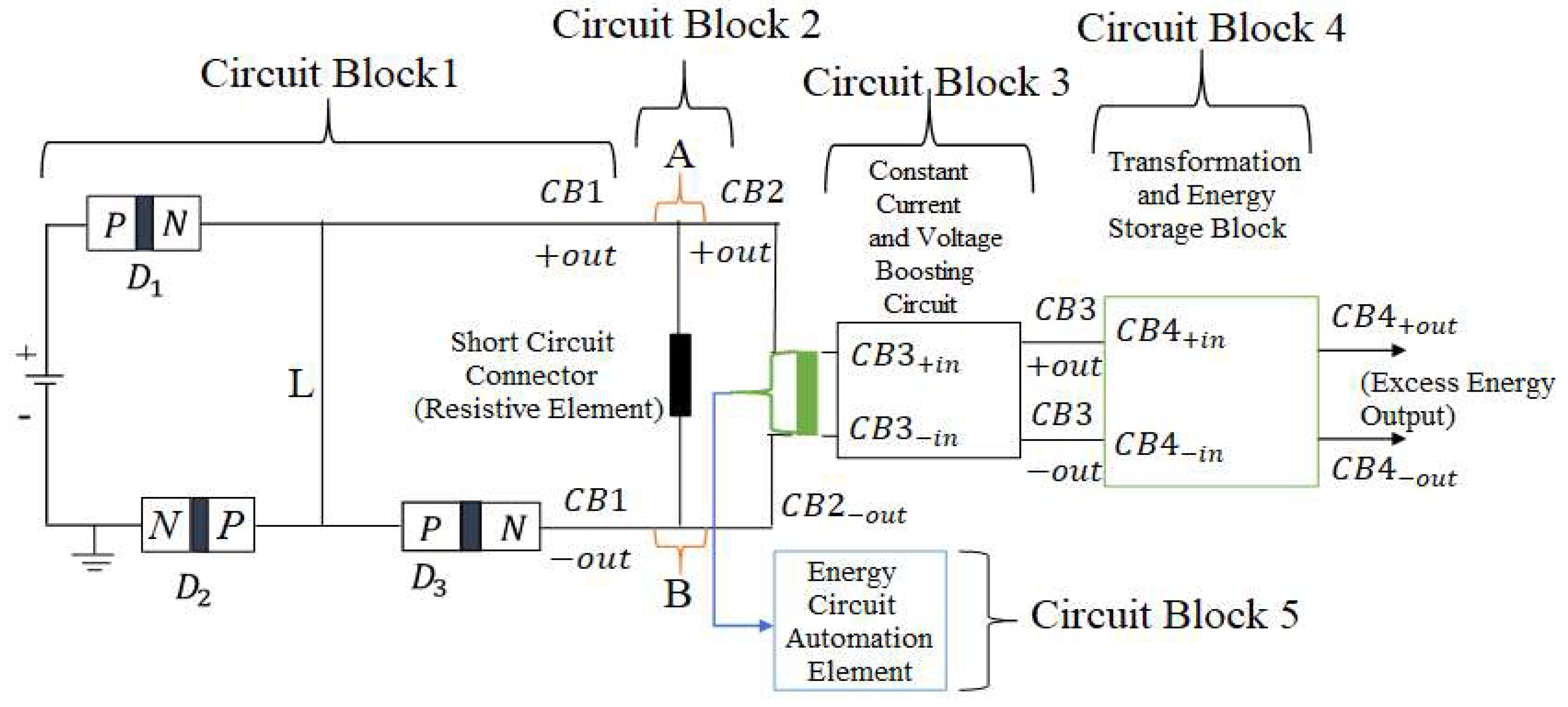
Figure 3.
Operational Principle of “Circuit Block 1”-Diode Configuration.
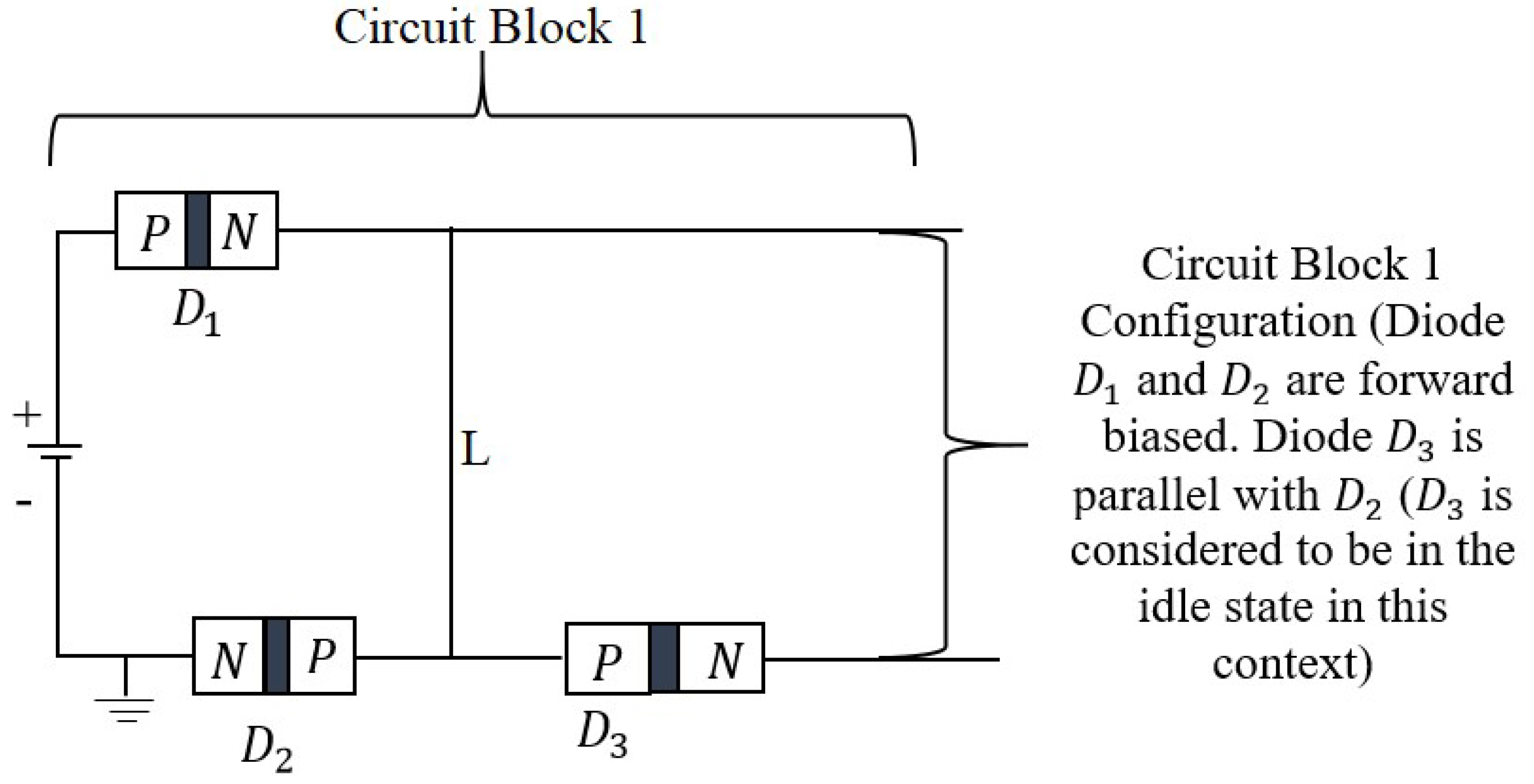
Figure 4.
“Circuit Block 2”-Short Circuit Power Harnessing. (“Circuit Block 2” illustrates the innovative approach to energy generation and conservation).
Figure 4.
“Circuit Block 2”-Short Circuit Power Harnessing. (“Circuit Block 2” illustrates the innovative approach to energy generation and conservation).
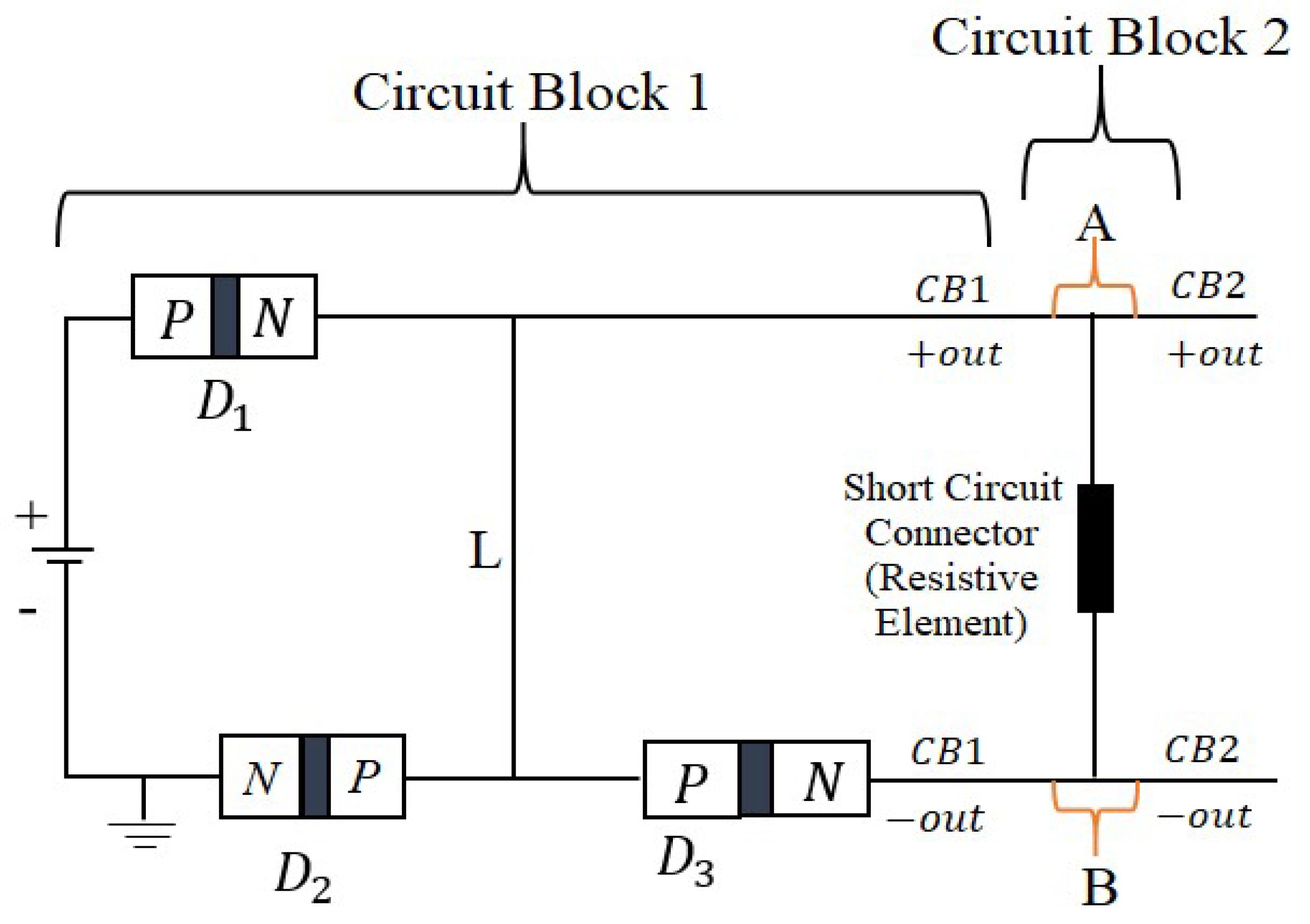
Figure 5.
Schematic diagram of the experimental energy-circuit, illustrating the connections between diodes , , and , as well as the short circuit connector at nodes and for “Circuit Block 2” and the measurement setup using the current sensor and Arduino Uno.
Figure 5.
Schematic diagram of the experimental energy-circuit, illustrating the connections between diodes , , and , as well as the short circuit connector at nodes and for “Circuit Block 2” and the measurement setup using the current sensor and Arduino Uno.
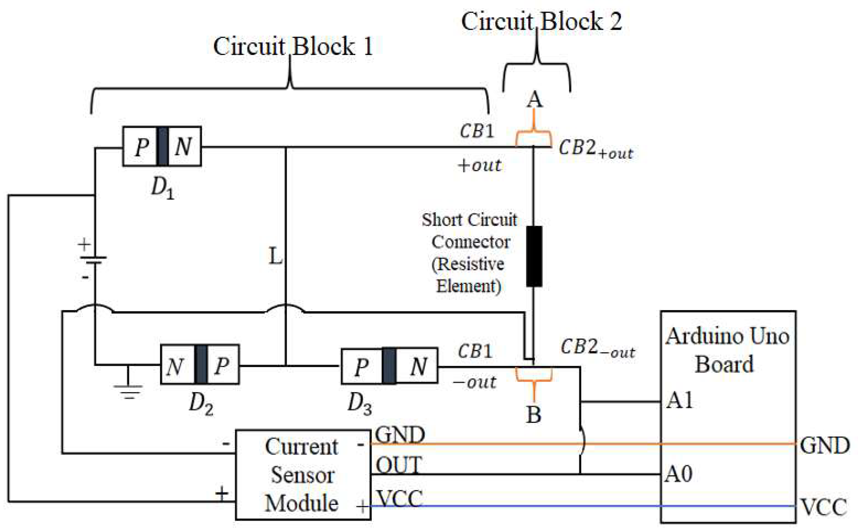
Figure 6.
Experimental results of “Circuit Block 2” during the short circuit event. ((a) Current behavior showing a stable increase to approximately , indicating the system's capacity to handle the short circuit without significant fluctuation; (b) Supply voltage, which drops from to around during the short circuit, demonstrating the expected voltage drop across the low-resistance path between diodes and ; (c) Power output fluctuating between and , illustrating the impact of voltage drops and recoveries on the overall power output during the short circuit).
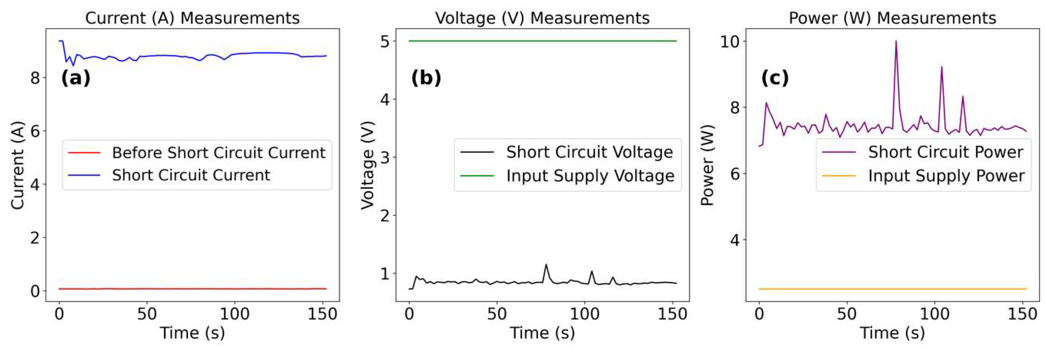
Figure 7.
“Circuit Block 3”-Energy Transformation and “Load Component_CB3”. (The block diagram illustrates the energy transformation process in “Circuit Block 3” providing a constant current boost converter for voltage amplification).
Figure 7.
“Circuit Block 3”-Energy Transformation and “Load Component_CB3”. (The block diagram illustrates the energy transformation process in “Circuit Block 3” providing a constant current boost converter for voltage amplification).
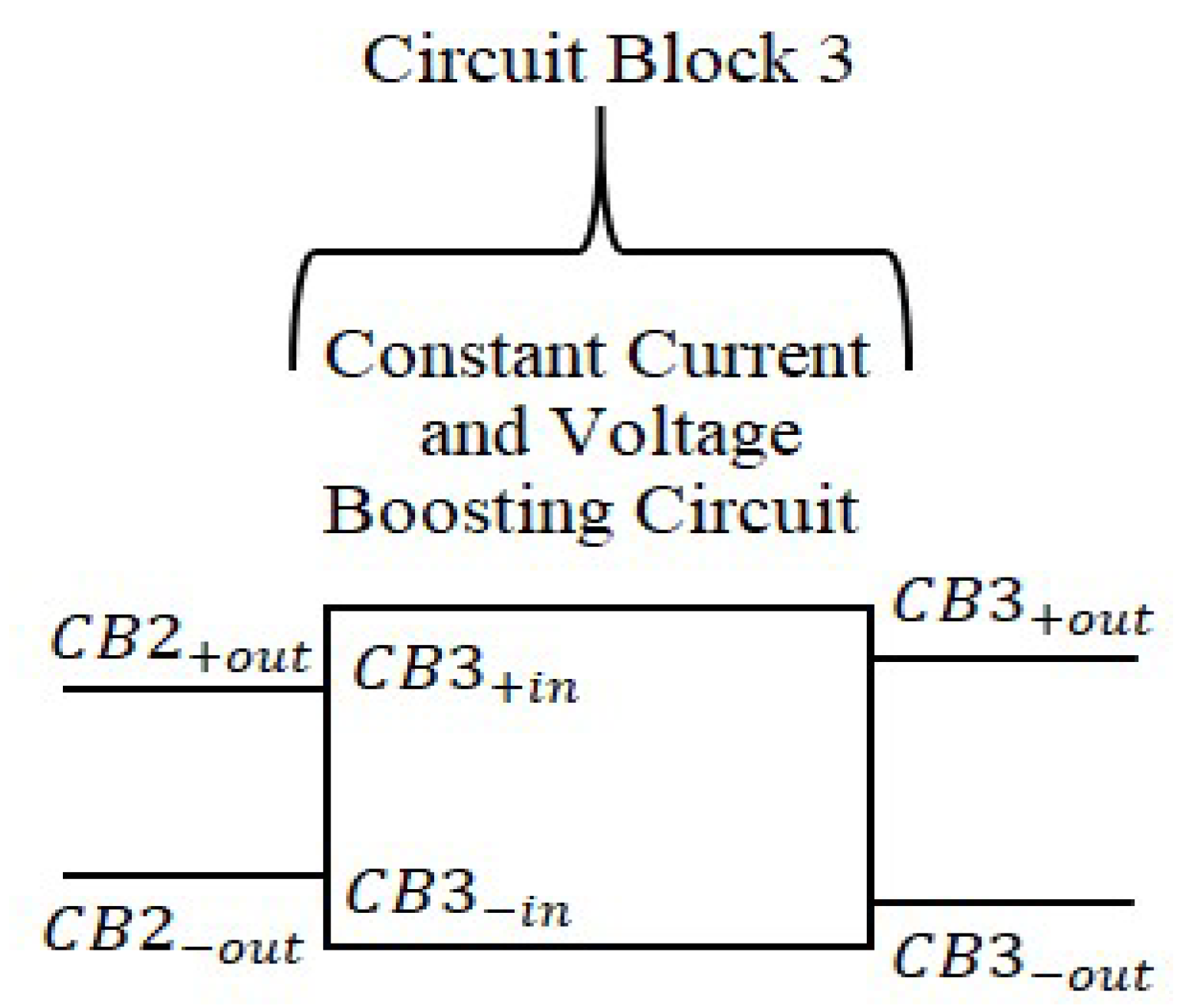
Figure 8.
“Circuit Block 4” Configuration-Energy Storage and Potential Recharging System (“Circuit Block 4” serves as a crucial interface in the energy conservation process, capturing output power from “Circuit Block 3” and overseeing its efficient utilization).
Figure 8.
“Circuit Block 4” Configuration-Energy Storage and Potential Recharging System (“Circuit Block 4” serves as a crucial interface in the energy conservation process, capturing output power from “Circuit Block 3” and overseeing its efficient utilization).
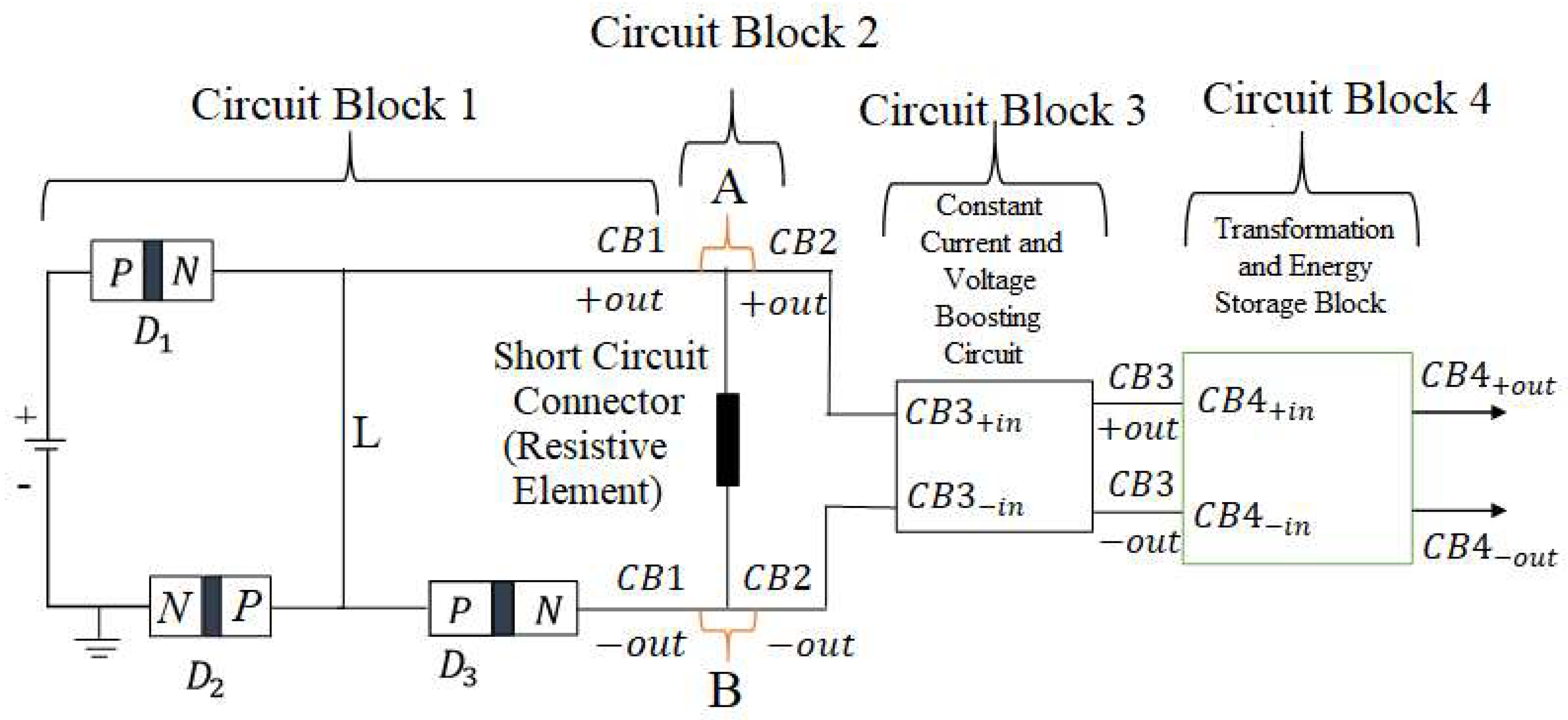
Figure 10.
Analysis of “Circuit Block 3” Power Output and Efficiency. (Figure 10(a) Signal energy comparison between the input () and output () power profiles, demonstrating the significant amplification of energy from input to output. Figure 10(b) Efficiency of “Circuit Block 3”, showing a high percentage of power conversion, which indicates the energy-circuit's exceptional ability to convert and amplify the supplied power with minimal losses).
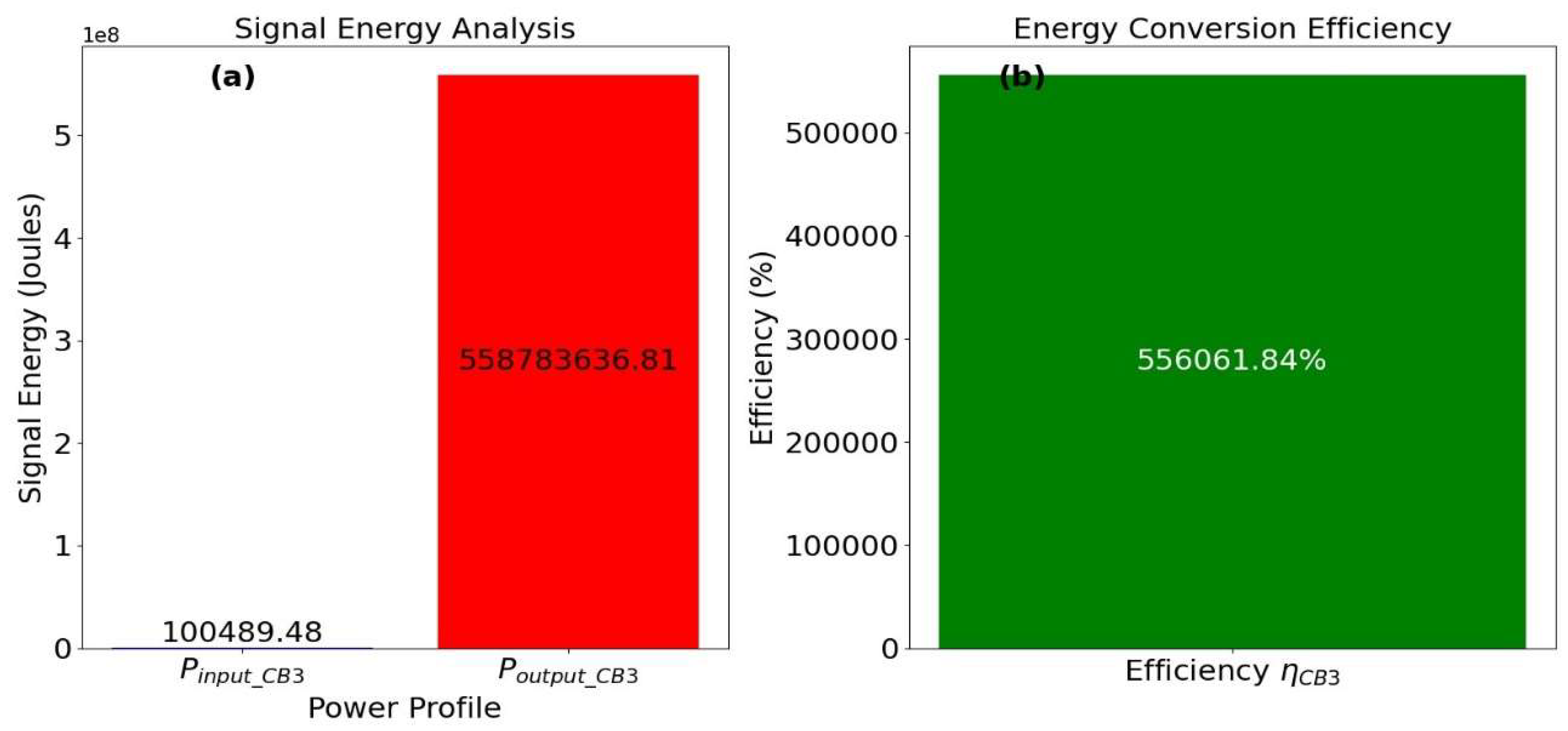
Figure 11.
Variation of Current and Power between Circuit Block 1 and Circuit Block 2. (This figure illustrates the transition of current and power between “Circuit Block 1” and “Circuit Block 2” in the simulated energy-circuit. The left subplot shows the variation of current (in Amperes) between the two blocks, highlighting the difference in current magnitude. The right subplot depicts the corresponding variation of power (in Watts), indicating the transformation of energy from input to output as it traverses through the energy-circuit compartments).
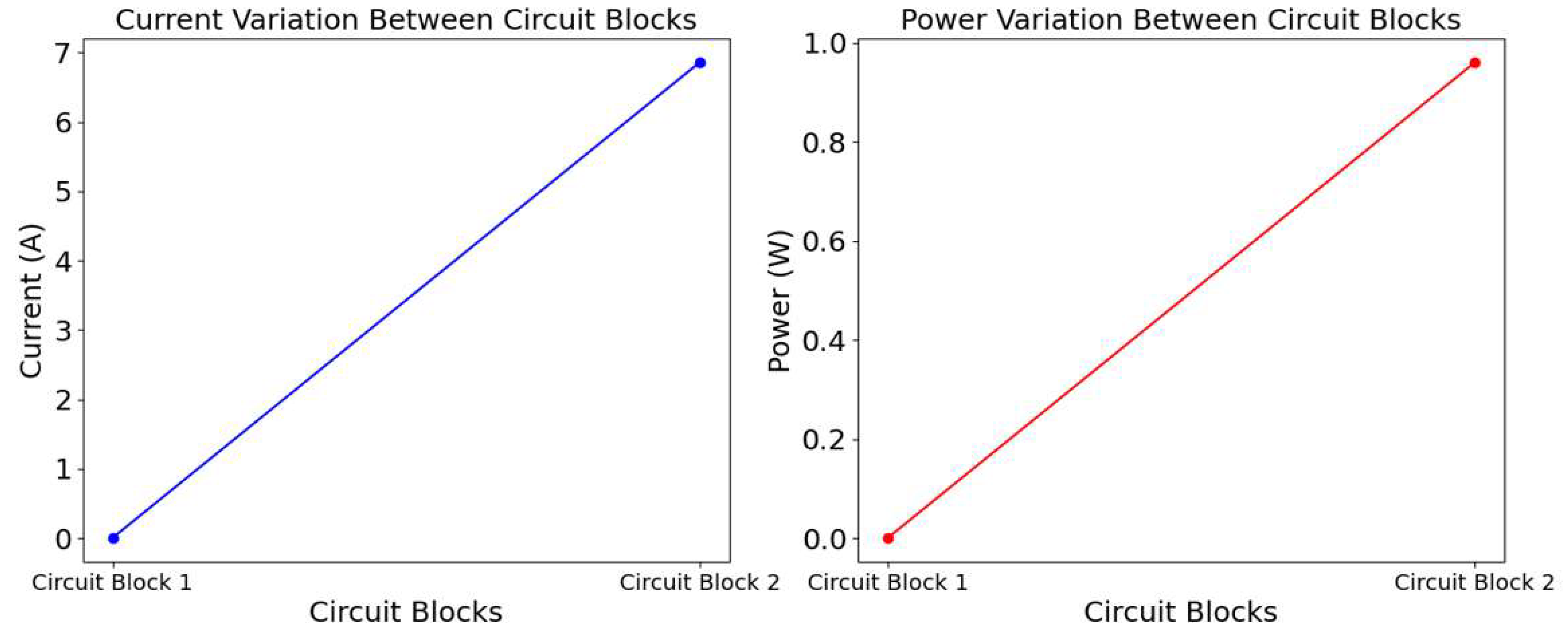

Table 1.
(baseline-experiment results). Measured Voltage and Current Outputs at Node Before and After Short Circuit.
Table 1.
(baseline-experiment results). Measured Voltage and Current Outputs at Node Before and After Short Circuit.
| Time (Seconds) | Before Short Circuit (V) | After Short Circuit (V) | Before Short Circuit (A) | After Short Circuit (A) |
|---|---|---|---|---|
| 0 | 2.478006 | 0.72825 | 0.06698 | 9.366438 |
| 2 | 2.468231 | 0.733138 | 0.066902 | 9.367899 |
| 4 | 2.468231 | 0.948192 | 0.067778 | 8.585144 |
| 7 | 2.468231 | 0.894428 | 0.064511 | 8.779899 |
| 9 | 2.463343 | 0.904203 | 0.066962 | 8.435441 |
| 11 | 2.458456 | 0.83089 | 0.066399 | 8.855851 |
| 14 | 2.468231 | 0.855328 | 0.066047 | 8.818721 |
| 16 | 2.463343 | 0.821114 | 0.063247 | 8.693515 |
| 18 | 2.473118 | 0.85044 | 0.06166 | 8.728211 |
| 21 | 2.468231 | 0.845552 | 0.065841 | 8.761161 |
| 23 | 2.463343 | 0.835777 | 0.071532 | 8.779221 |
| 25 | 2.468231 | 0.860215 | 0.060346 | 8.756813 |
| 28 | 2.458456 | 0.85044 | 0.070349 | 8.712845 |
| 30 | 2.468231 | 0.855328 | 0.073433 | 8.678877 |
| 32 | 2.468231 | 0.821114 | 0.072344 | 8.788436 |
| 35 | 2.458456 | 0.85044 | 0.070614 | 8.769209 |
| 37 | 2.458456 | 0.855328 | 0.06983 | 8.729052 |
| 40 | 2.468231 | 0.835777 | 0.067536 | 8.636889 |
Table 2.
Simulation Results for Proposed Energy-circuit Blocks and the ohmic transformed power output.
Table 2.
Simulation Results for Proposed Energy-circuit Blocks and the ohmic transformed power output.
| Supply Voltage (V) | Diode Forward Voltage (V) | (Ohms) | Ideality Factor (n) | ) (A) | (Ohms) | (Ohms) | A) | (V) | (V) | (A) | W) | (W) |
|---|---|---|---|---|---|---|---|---|---|---|---|---|
| 5.000 | 1.18 | 1.0 | 1.2 | 5.670 | 0.00398 | 308.07 | 0.48 | 1.26 | 5.0199 | 150.61 | 143.005 | |
| 7.111 | 1.20 | 2.0 | 1.3 | 12.499 | 0.00253 | 60.15 | 0.49 | 1.28 | 3.5600 | 29.90 | 158.453 | |
| 9.222 | 1.22 | 1.5 | 1.1 | 7.099 | 0.00285 | 59356.48 | 0.50 | 1.30 | 6.1598 | 30001.49 | 269.476 | |
| 11.333 | 1.21 | 2.5 | 1.4 | 13.980 | 0.00248 | 9.32 | 0.50 | 1.29 | 4.5378 | 4.67 | 287.938 | |
| 13.444 | 1.19 | 1.8 | 1.2 | 7.051 | 0.00230 | 1062.50 | 0.49 | 1.27 | 7.4787 | 523.83 | 394.520 | |
| 15.555 | 1.23 | 3.0 | 1.5 | 6.906 | 0.00301 | 2.24 | 0.50 | 1.31 | 5.1904 | 1.14 | 186.154 | |
| 17.666 | 1.20 | 2.2 | 1.3 | 5.365 | 0.00119 | 105.27 | 0.49 | 1.28 | 8.0346 | 52.34 | 346.452 | |
| 19.777 | 1.22 | 4.0 | 1.6 | 9.720 | 0.00131 | 0.30 | 0.50 | 1.30 | 4.9460 | 0.15 | 237.835 | |
| 21.888 | 1.21 | 2.7 | 1.4 | 10.648 | 0.00437 | 13.98 | 0.50 | 1.29 | 8.1201 | 7.01 | 702.411 | |
| 24.000 | 1.19 | 3.5 | 1.7 | 5.657 | 0.00475 | 0.03 | 0.49 | 1.27 | 6.8664 | 0.01 | 266.946 |
Disclaimer/Publisher’s Note: The statements, opinions and data contained in all publications are solely those of the individual author(s) and contributor(s) and not of MDPI and/or the editor(s). MDPI and/or the editor(s) disclaim responsibility for any injury to people or property resulting from any ideas, methods, instructions or products referred to in the content. |
© 2024 by the authors. Licensee MDPI, Basel, Switzerland. This article is an open access article distributed under the terms and conditions of the Creative Commons Attribution (CC BY) license (http://creativecommons.org/licenses/by/4.0/).
Copyright: This open access article is published under a Creative Commons CC BY 4.0 license, which permit the free download, distribution, and reuse, provided that the author and preprint are cited in any reuse.


