Submitted:
18 August 2023
Posted:
18 August 2023
You are already at the latest version
Abstract
Copper-nitride (Cu3N) material is attracting much attention as a potential next-generation thin-film solar-light absorber. In this work, polycrystalline Cu3N thin films were prepared using reactive-RF-magnetron sputtering, at room temperature,onto glass and silicon substrates. The optical properties of the Cu3N thin layers were studied by spectroscopic ellipsometry and transmission, to achieve a low-cost absorber material to replace conventional silicon. The reactive-RF-sputtered Cu3N films were also investigated by FIB-SEM microscopy and FTIR spectroscopy.
Keywords:
Optical properties
; thin films
; electron microscopy
; spectroscopic ellipsometry
; solar energy
1. Introduction
There is a need to innovate in eco-friendly, advanced materials to provide the answer to the social demand for sustainable energy [1,2,3]. Determination and understanding of the optical properties of polycrystalline copper-nitride (CuN) thin films, such as refractive index and extinction coefficient and band-gap energy, are important to carry out a photovoltaic-cell design, in which the CuN material acts as solar-light absorber [4,5]. It would open the door to the next, flexible third-generation of photovoltaic technologies that could benefit from this material. The practical application of copper-nitride layers mainly depends upon the size of its optical band gap. This nitride is an non-toxic choice to consider as a possible alternative for tellurium-based materials.
On the novelty of this study, despite the great expectations that the metastable indirect-gap CuN semiconductor is awakening because of its optical and energy-storage properties, it is not yet employed in a specific solar cell. The development of low-cost CuN semiconductor, free of critical materials, and prepared with easy growth techniques for industrial scaling, such as reactive-RF-magnetron-sputtering deposition, is nowadays considered a hot topic in emerging-technology photovoltaics.
The present work reports the successful preparation of the CuN compound, with an anti-ReO cubic crystal structure, at room temperature, and using two gaseous environments: (i) an Ar-free environment, based upon nitrogen (N), and (ii) a mix of N and Ar. Scanning electron microscopy was employed to determine the surface morphology of CuN samples. We then calculated the optical constants of the copper-nitride layers using UV-MIR spectroscopic ellipsometry [6,7,8].
2. Experimental
We grew CuN films by reactive radio-frequency magnetron sputtering, at room temperature, 50-W RF-power, and working gas pressure of 5.0 Pa, onto glass and silicon substrates; we used partial nitrogen pressures of 0.8 and 1.0. Details regarding the deposition conditions are listed in Table 1.
Scanning electron microscopy (FIB-SEM) was employed to study the topography of CuN layers. The focused-ion-beam technique was used to obtain transversal trenches and remove material from the surface, for measuring pore sizes using the software ImageJ. Further details are found elsewhere [5].
UV-Visible-NIR spectroscopic ellipsometry (SE) measurements were used to acquire the ellipsometric angles and , on a Woollam vertical variable-angle-of-incidence rotating-analyzer ellipsometer. Data were obtained at three angles 50, 60, and 70, respectively. Infrared spectroscopic ellipsometry (IRSE) measurements were also carried out on a Woollam IR-VASE Mark II ellipsometer, integrating a Fourier-transform infrared interferometer source. The experimental IRSE and SE data were modeled using the WVASE software package, version 3.942. FTIR measurements were performed using a Perkin-Elmer 100 FTIR spectrometer.
3. Results and discussion
3.1. FIB-SEM Microscopy Study
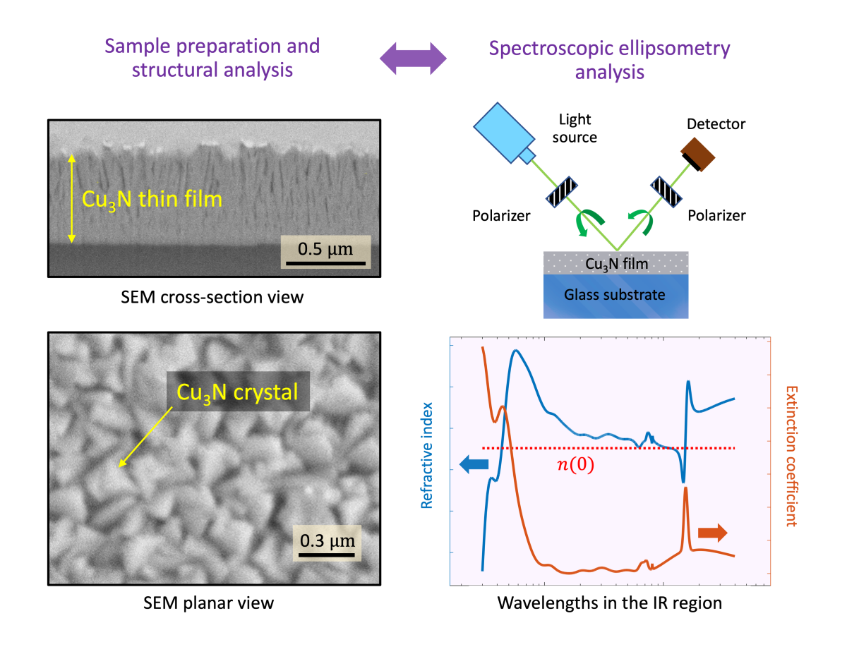
The CuN films exhibited a columnar formation, as shown in Figure 1a. It is observed that the copper-nitride microstructure through about the first 100 nm (samples #1460 and #1490), or around the first 200 nm (sample #1360) from the glass surface is compacted, while voided spaces between the CuN-layer columns are clear in the rest of thickness. This columnar-structure ‘zone’ 2 of the Thornton zone model [9], and consists of columnar and compact grains with high density and smooth surfaces. It results from being grown at room temperature and low working-gas pressure. Figure 1b displays an SEM micrograph of the surface of sample #1460. CuN pillars met at its surface, giving place to a conglomerated structure with many closed pores.
The porosity of sample #1360 was quantified using images such as the one in Figure 1c. The pore map in Figure 1d was obtained using the software ImageJ from the region indicated by a dashed frame in Figure 1c. This software is commonly utilized to measure particle sizes from images. It has successfully been used in this work similarly to obtain the equivalent pore radii. Figure 1d shows the pore perimeter (black lines) and the numbering (in red) that ImageJ uses to identify each pore. Pore areas, , were automatically measured from the map, and the values of the equivalent radii were obtained using . The inset in Figure 1d is the histogram for the values calculated from the SEM image in Figure 1c: The mean equivalent radius was 10.4 ± 4.7 nm.
3.2. Spectro-Ellipsometric Analysis
Additionally, optical data were fit over the range of 200-40,000 nm (0.031-6.2 eV), simultaneously transmission data (200-2500 nm, or 0.5-6.2 eV). The best-fit ellipsometric model required in the sample #1490 has a 46-nm surface roughness (Table 1).
Figure 2 shows the best-fit optical constants n and k for CuN samples, using a seven-oscillator model in the particular #1490 specimen; Table 1 gives information about the oscillators for all CuN samples. Two major spectral features are seen in the optical constants of CuN: A UV-Visible absorption edge with a peak at approximately 2.47 eV, and a second sharp resonant absorption in the infrared near 15,480 nm, both for the #1490 layer. The UV-Visible edge with a clear peak was modeled by combining a Gaussian and a Tauc-Lorentz [10,11,12] oscillator. Five Gaussian oscillators were added to fit the two ellipsometric angles and the transmission data for the #1490 sample. The extremely-sharp resonant absorption peak at 646 cm (Figure 2c), suggests that this sample is polycrystalline. This peak was modeled using a Gaussian oscillator, though it could also have been used, instead of a Gaussian oscillator, a Lorentz oscillator.
Dielectrics and semiconductors are generally transparent at near-IR (NIR) wavelengths. These materials absorb light in the UV and visible ranges due to valence-electron transitions. Many will also show the IR absorbance due to the presence of phonons, or free carriers. Figure 2 shows the broadband optical constants for CuN for the first time to the best of our knowledge, and illustrates the UV-Visible absorption due to the valence-electron transitions. Moreover, copper-nitride quasi-transparent across the remaining visible and NIR regions, until the phonon occurs in the middle-infrared range.
For comparison the CuN samples were also analyzed by FTIR transmission spectroscopy. The FTIR absorbance spectra are shown in Figure 3b. The positions of the corresponding CuN-phonon mode are all of them at around 645 cm, in excellent agreement indeed with those independently calculated by infrared ellipsometry (i.e. this single band confirmed the creation of the Cu-N bond). This would be indicate that the amount of N was adequate to form the CuN phase. A weak peak around 835 cm, assigned to the Cu-N bond, was also observed in all cases. In addition, a peak at 2049 cm (not shown in Figure 3a) appeared in the FTIR spectra, corresponding to the stretching vibration of the N-azide.
Concerning the UV-Visible absorption edge, Figure 3b displays the absorption coefficient spectrum, versus photon energy for the three CuN, calculated from ellipsometric and transmission measurements. These plots allow us to determine the iso-absorption gap , the energy value at which . The obtained values of Urbach energy [13] are listed in Table 1. The isoabsorption gap , for being empirical, is less sensitive to interpretational difficulties corresponding the optical band gap and, therefore, is in use as a common definition of the band gap in polycrystalline semiconductors.
3.3. Single-Effective-Oscillator Model
We focus next on fitting the CuN refractive-index dispersion below the band gap to the Wemple-DiDomenico single-effective-oscillator expression [14]:
where is the energy of the effective dispersion oscillator, and is the dispersion energy. By plotting versus (Figure 3a), the parameters and were determined.
The dispersion parameters and are indicated in Figure 3a. The oscillator energy is an ‘average’ energy gap. For the dispersion energy , a relationship [14] was proposed:
where is a two-valued constant, 0.37 ± 0.04 eV for covalent materials, and 0.26 ± 0.03 eV for more ionic materials. is the coordination number of the cation nearest neighbor to the anion (), is the formal valency of the anion (), and is the effective number of valence electrons per anion. In the CuN compound,
We are not including the Cu d-electrons in our ‘electron count’ [14].
The particular value of obtained by the previous Wemple-DiDomenico expression is 17.8 eV. The differences with the values presented in Figure 3a, especially in the most-discrepant case of sample #1360, can be explained by the reported lack of stoichiometry of CuN films (Cu/N-ratio was smaller than the expected ratio of 3) [4]. Moreover, the long-wavelength value of the refractive index, displayed in Figure 2, is given by
Significantly, the values of these static refractive indices are consistent with the data obtained by the UV-MIR ellipsometry (see Figure 2).
The correspondence between the Wemple-DiDomenico parameter, , and the optical band gap, , is generally expressed as [15]. For CuN compound the value of obtained from goes from 1.50 eV for sample #1360 to 1.73 eV for sample #1460.
4. Conclusions
This study has demonstrated the usefulness of the wide-spectral coverage of state-of-art ellipsometry, allowing the determination of the optical properties in the UV, visible, and infrared ranges using only one technique. Adding transmission has increased sensitivity to small absorption features in our RF-magnetron-sputtered CuN. Based on FIB-SEM microscopy, the CuN structure was described, following the Thornton model. The iso-absorption gaps (thus avoiding the use of the sometimes ill-defined optical-band-gap parameter), exhibited a strong dependence upon growth conditions. A material with values of between 1.3 eV and 1.8 eV is suitable as a solar-light absorber.
Author Contributions
E. Márquez: conceptulization, methodology, writing (original draft). E. Blanco: methodology, formal analysis, software. J.M. Mánuel: methodology, formal analysis, software. M. Ballester: software, visualization, writing (review and editing). M. García-Gurrea: software, visualization, writing (review and editing). S.M. Fernández: investigation, data curation, resources, funding acquisition. M.I. Rodríguez-Tapiado: investigation, data curation, funding acquisition. F. Willomitzer: Supervision, validation, writting (review and editing). A.K. Katsaggelos: supervision, validation, writing, (review and editing).
Funding
This study received financial support from MCIN/AEI/10.13039/501100011033, under grant PID2019-109215RB-C42. This funding is part of the economic recovery investment and reform measures under the Next Generation EU.
Data Availability Statement
The data employed in this study can be obtained from the corresponding author upon request.
Acknowledgments
The authors thank Dr. L. González-Souto for their invaluable assistance. J.M. Mánuel wishes to express gratitude to the “Central Service for Research in Science and Technology” (SC-ICYT) at the University of Cádiz.
Conflicts of Interest
The authors confirm that there are no conflicts of interest associated with this publication.
References
- Aihua, J.; Meng, Q.; Jianrong, X. Preparation, structure, properties, and application of copper nitride (Cu3N) thin films: A review. J. Mater. Sci. Technol. 2018, 34, 1467–1473. [Google Scholar]
- Zakutayev, A. Design of nitride semiconductors for solar energy conversion. J. Mater. Chem. A 2016, 4, 6742–6754. [Google Scholar] [CrossRef]
- Borsa, D.; Boerma, D. Growth, structural and optical properties of Cu3N films. Surf. Sci. 2004, 548, 95–105. [Google Scholar] [CrossRef]
- Rodríguez-Tapiador, M.I.; Merino, J.; Jawhari, T.; Muñoz-Rosas, A.L.; Bertomeu, J.; Fernández, S. Impact of the RF Power on the Copper Nitride Films Deposited in a Pure Nitrogen Environment for Applications as Eco-Friendly Solar Absorber. Materials 2023, 16, 1508. [Google Scholar] [CrossRef]
- Márquez, E.; Blanco, E.; García-Gurrea, M.; Cintado Puerta, M.; Domínguez de la Vega, M.; Ballester, M.; Mánuel, J.; Rodríguez-Tapiador, M.; Fernández, S. Optical Properties of Reactive RF Magnetron Sputtered Polycrystalline Cu3N Thin Films Determined by UV/Visible/NIR Spectroscopic Ellipsometry: An Eco-Friendly Solar Light Absorber. Coatings 2023, 13, 1148. [Google Scholar] [CrossRef]
- Tompkins, H.G.; Hilfiker, J.N. Spectroscopic ellipsometry: practical application to thin film characterization; Momentum Press, 2015. [Google Scholar]
- Blanco, E.; Domínguez, M.; González-Leal, J.; Márquez, E.; Outón, J.; Ramírez-del Solar, M. Insights into the annealing process of sol-gel TiO2 films leading to anatase development: The interrelationship between microstructure and optical properties. Appl. Surf. Sci. 2018, 439, 736–748. [Google Scholar] [CrossRef]
- Márquez, E.; Blanco, E.; García-Vázquez, C.; Díaz, J.; Saugar, E. Spectroscopic ellipsometry study of non-hydrogenated fully amorphous silicon films deposited by room-temperature radio-frequency magnetron sputtering on glass: Influence of the argon pressure. J. Non Cryst. Solids 2020, 547, 120305. [Google Scholar] [CrossRef]
- Thornton, J.A. High Rate Thick Film Growth. Annu. Rev. Mater. Res. 1977, 7, 239–260. [Google Scholar] [CrossRef]
- Jellison Jr, G.E.; Modine, F.A. Parameterization of the optical functions of amorphous materials in the interband region. Appl. Phys. Lett. 1996, 69, 371. [Google Scholar] [CrossRef]
- Ballester, M.; García, M.; Márquez, A.P.; Blanco, E.; Minkov, D.; Fernández-Ruano, S.; Willomitzer, F.; Cossairt, O.; Márquez, E. Application of the Holomorphic Tauc-Lorentz-Urbach Function to Extract the Optical Constants of Amorphous Semiconductor Thin Films. Coatings 2022, 12, 1549. [Google Scholar] [CrossRef]
- Marquez, E.; Ballester, M.; Garcia, M.; Cintado, M.; Marquez, A.; Ruiz, J.; Fernández, S.; Blanco, E.; Willomitzer, F.; Katsaggelos, A. Complex dielectric function of H-free a-Si films: Photovoltaic light absorber. Mater. Lett. 2023, 345, 134485. [Google Scholar] [CrossRef]
- Urbach, F. The Long-Wavelength Edge of Photographic Sensitivity and of the Electronic Absorption of Solids. Phys. Rev. 1953, 92, 1324. [Google Scholar] [CrossRef]
- Wemple, S.; DiDomenico Jr, M. Behavior of the electronic dielectric constant in covalent and ionic materials. Phys. Rev. B 1971, 3, 1338. [Google Scholar] [CrossRef]
- Tanaka, K. Optical properties and photoinduced changes in amorphous AsS films. Thin Solid Films 1980, 66, 271–279. [Google Scholar] [CrossRef]
Figure 1.
SEM micrographs of (a) cross-section and (b) planar views, both of sample #1490. (c) SEM image revealing the internal porosity of sample #1360, and (d) a pore size map obtained using “ImageJ” software, with (e) its associated histogram for the pore equivalent radii.
Figure 1.
SEM micrographs of (a) cross-section and (b) planar views, both of sample #1490. (c) SEM image revealing the internal porosity of sample #1360, and (d) a pore size map obtained using “ImageJ” software, with (e) its associated histogram for the pore equivalent radii.
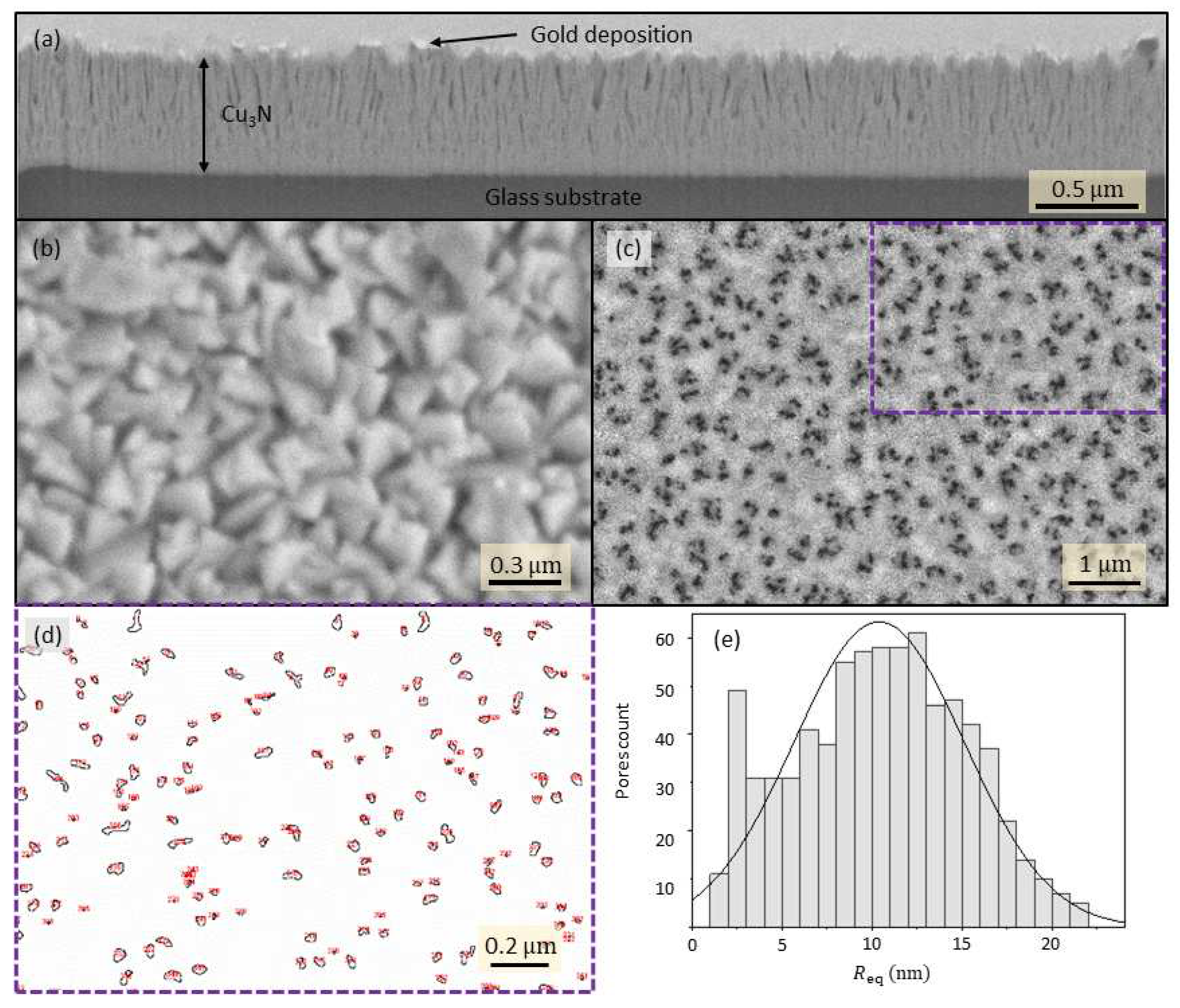
Figure 2.
(a) A representative sample photo, and (b) a schematic ellipsometry set-up. Optical functions n and k of samples (c) #1360, (d) #1460, (e) #1490. (f) The log-log scale of sample #1490.
Figure 2.
(a) A representative sample photo, and (b) a schematic ellipsometry set-up. Optical functions n and k of samples (c) #1360, (d) #1460, (e) #1490. (f) The log-log scale of sample #1490.
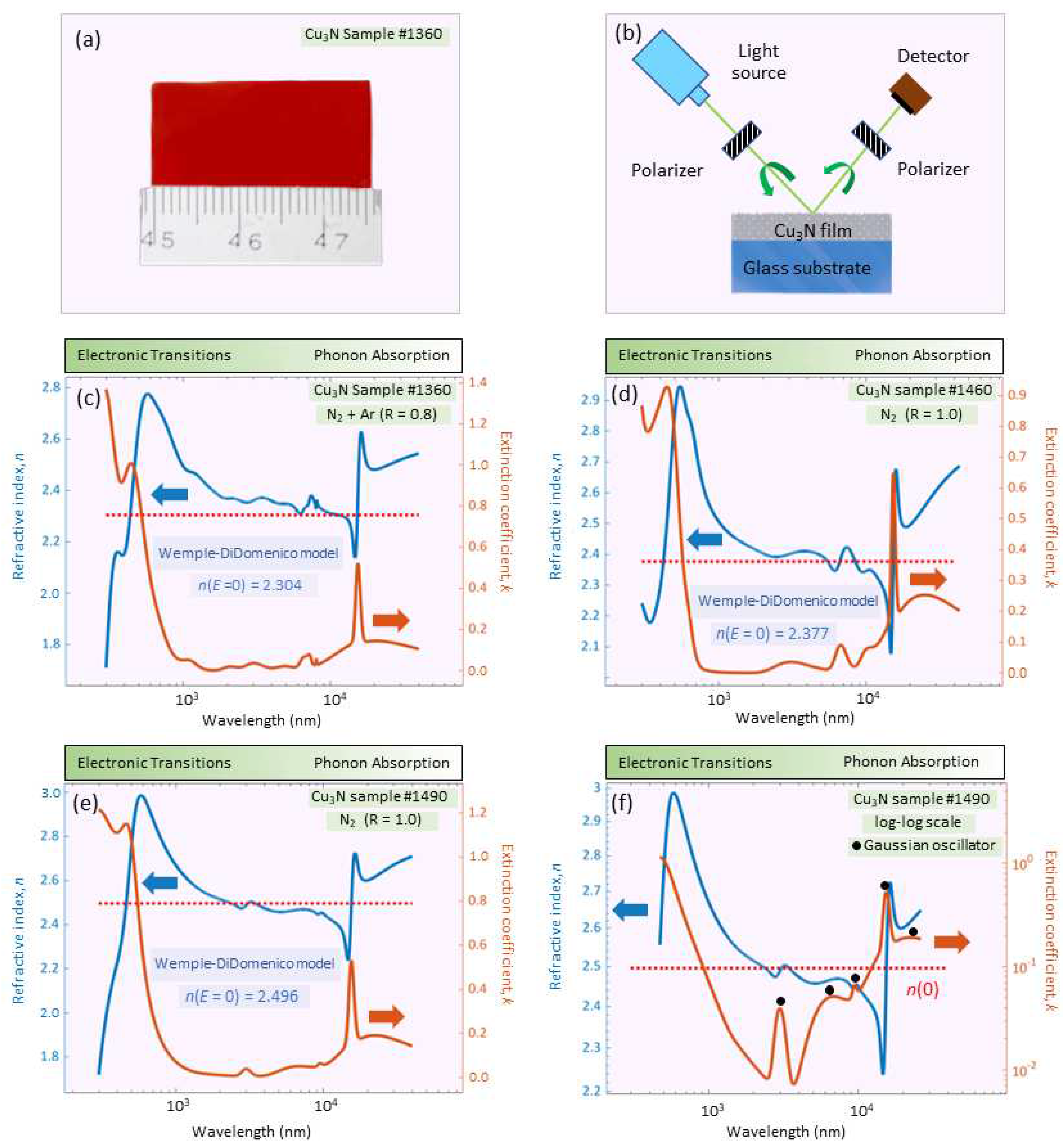
Figure 3.
(a) FTIR spectra of CuN. (b) Wemple-DiDomenico plots. (c) Optical-absorption edges.
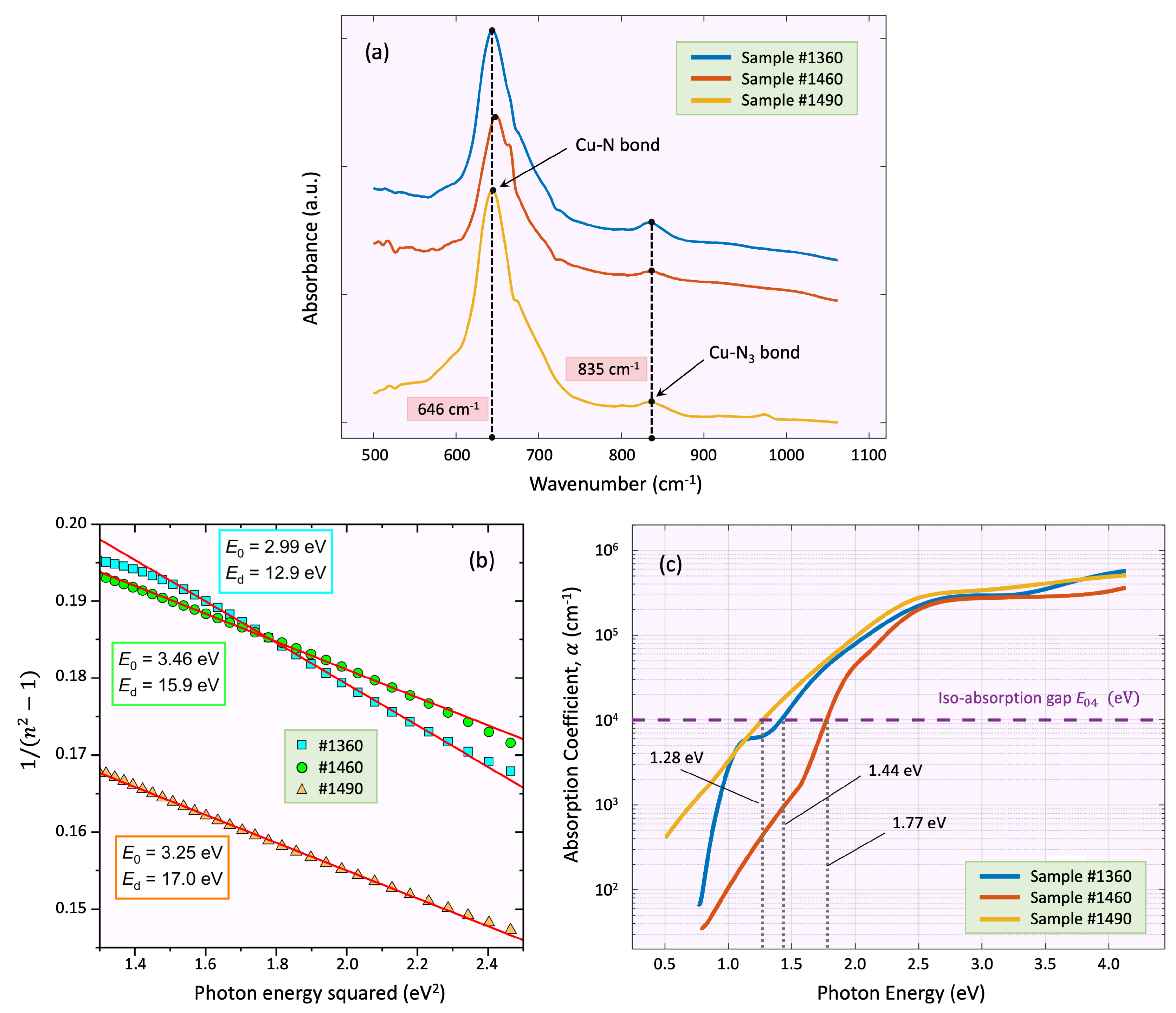

Table 1.
Deposition conditions for CuN films and their optical properties.
| Sample | N flux | Ar flux | Partial N | Deposition | Total oscillators | Sample | Sample | Urbach |
|---|---|---|---|---|---|---|---|---|
| ID | (sccm) | (sccm) | pressure | time (min) | (TL + Gaussian) | thickness (nm) | roughness (nm) | energy (meV) |
| #1360 | 20 | 10 | 0.8 | 60 | 12 (1 + 11) | 430 | 42 | 96 |
| #1460 | 20 | 0 | 1.0 | 60 | 9 (1 + 8) | 333 | 22 | 176 |
| #1490 | 20 | 0 | 1.0 | 90 | 7 (1 + 6) | 610 | 46 | 242 |
Disclaimer/Publisher’s Note: The statements, opinions and data contained in all publications are solely those of the individual author(s) and contributor(s) and not of MDPI and/or the editor(s). MDPI and/or the editor(s) disclaim responsibility for any injury to people or property resulting from any ideas, methods, instructions or products referred to in the content. |
© 2022 by the authors. Licensee MDPI, Basel, Switzerland. This article is an open access article distributed under the terms and conditions of the Creative Commons Attribution (CC BY) license (https://creativecommons.org/licenses/by/4.0/).
Copyright: This open access article is published under a Creative Commons CC BY 4.0 license, which permit the free download, distribution, and reuse, provided that the author and preprint are cited in any reuse.


