
Submitted:
18 July 2023
Posted:
19 July 2023
You are already at the latest version
Abstract
Systematic results of lattice dynamical calculation are reported for the novel (SiC)m/(GeC)n superlattices (SLs) by exploiting a modified-linear chain model (M-LCM) and a realistic rigid-ion- model (RIM). By employing the bond polarizability method in the framework of M-LCM, we have simulated Raman intensities for the graded (SiC)10-D/(Si0.5Ge0.5C)D/(GeC)10-D/(Si0.5Ge0.5C)D SLs by carefully integrating interfacial layer thickness D (≡ 0, 1, 2, 3 monolayers (MLs)). The variation of D has initiated considerable up (down) shifts of GeC-, (SiC)-like Raman peaks in the middle of the optical phonon frequency region. With D = 3 MLs, the maximum energy shift (by ~ 47 cm-1) of SiC-like modes has caused substantial changes in the Raman intensity profiles linked to the localization of atomic displacements at the interfacial transition regions. This effect can be considered as a vital tool for authenticating the interfacial structures in technologically important SLs. By using a RIM, we have reported SL phonon dispersions along the growth [001] as well as in the plane [100], [110] perpendicular to the growth. Our simulations of phonons in the acoustic mode region have not only confirmed the formation of minigaps at the zone center and zone edges but also provided evidence of anti-crossing and phonon confinement. Besides examining angular dependence of zone-center optical modes, we have also discussed phonon folding, confinement and anisotropic behavior in (SiC)m/(GeC)n SLs.
Keywords:
novel (SiC)m/(GeC)n superlattices
; interfacial layer thickness
; raman intensity profiles
; lattice dynamics
; localization of atomic displacements
1. Introduction
Semiconductor quantum wells (QWs) and superlattices (SLs) have formed the basis of fabricating many modern electronics and optoelectronic devices, including the light emitting diodes (LEDs), laser diodes (LDs), field-effect transistors (FETs) etc. [1,2,3,4,5,6,7,8,9,10] As compared to II-VI and III-V compounds, the epitaxial growth of C-based zinc-blende (zb) IV-IV (XC with X = Si, Ge, Sn) binary materials, alloys, QWs and SLs of higher thermal conductivity, higher mechanical strength, and wider electronic energy bandgaps have recently stimulated interests among the technologists to design different types of device structures (e.g., meta-photonics-heterostructure, holographic displays, lasers, etc.) and for scientists to evaluate their basic traits. [1,2,3,4,5,6,7,8,9,10] The progress in device engineering has demanded careful selection of the C-based materials which maintain physical properties both at elevated temperatures and higher radiation levels. [2,3,4,5,6,7,8,9] In graded hetero-structures, the role of nano-crystallite interfaces is known to have strong impact on many of their optical and/or electro-optical characteristics. Enormous challenges still exist to monitor and estimate interfacial layer thickness. Simulation of phonons at atomic interfaces in strained layer (SiC)m/(GeC)n SLs is viewed as a major step forward for realizing the heat transport in thermal-management strategy and to design high-performance thermoelectric nano/micro-electronics, as well as optoelectronic devices. [1,2,3,4,5,6,7,8,9,10]
A few theoretical reports exist on studying the structural, electronic, and optical properties of binary XC materials. [8,9,10,11,12,13,14,15,16,17,18,19,20] Limited reports are known to assess the lattice dynamical behavior of C-based alloys. [15,16,17,18,19,20] However, there are absolutely no attempts made to comprehend the phonon traits of novel (SiC)m/(GeC)n SLs. Using experimental and theoretical methods, some improvements are achieved by addressing the necessary constraints to secure progress in III-N and IV-IV based heterostructure [21,22,23] devices. Despite the exploitation of many optical and electrical methods, the estimation of graded interfacial thickness in strained-layer SLs is still a big challenge. Earlier, high-resolution transmission electron microscopy (HR-TEM) was used to map the distribution of In in GaN/In0.43Ga0.57N/ Al0.1Ga0.9N QW. [21] Irregular distribution of In forming nanoclusters was detected with the estimated diameters of 1-2 nm at GaN/InN, InGaN/AlGaN interfaces. In probing the optical, structural, and electrical attributes of III-V compound semiconductors, it has been a customary tradition to instigate a variety of characterization techniques including the reflectivity, absorption, [24,25,26,27] high resolution x-ray diffraction (HR-XRD), [28,29,30,31,32,33,34] extended x-ray absorption fine structures (EXAFs), [35,36,37,38,39,40] photoluminescence (PL), [42,43] secondary ion mass spectroscopy [20,21,22,23,24,25,26,27,28] (SIMS), spectroscopic ellipsometry (SE), [28] and electron-energy loss (EEL) [43,44] measurements, etc. Spectroscopic methods such as electron paramagnetic resonance (EPR) and far infrared (FIR) spectroscopy [21,22,23] have also been considered effective for probing the nature of electronic centers as well as assessing the nano-structured interfacial components by evaluating their vibrational and/or optical properties [24,25,26,27,28,29,30,31,32,33,34,35,36,37,38,39,40,41,42,43,44]
In this context, the Raman scattering spectroscopy (RSS) [45,46,47,48,49,50,51,52,53] is considered as one of the most valuable techniques for identifying the vibrational characteristics of short period SLs as the observed acoustic and optical phonon features display strong dependence on the arrangement of their constituents. [21,45,46,47] While the acoustic part of the phonon spectrum is sensitive to a large-scale preparation of SLs (i.e., their overall periodicity (m, n), capping and buffer layer thickness, etc.), the optical phonon spectra is dependent on their unit cells including, individual layer thickness and interfacial roughness. [45,46,47,48,49,50,51,52,53] Earlier RSS measurements in GaN/AlxGa1-xN SLs [21] have provided strong evidence of graded alloy interface region by an order of ~2 nm. The studies in (InN)m/(AlN)n, (GaN)m/ (AlN)n and (SiC)m/(Si)n heterostructures have confirmed that: (a) the interfacial effects lift optical phonon degeneracies to cause considerable gain in Raman intensities, and (b) a suitable choice of layer thickness of constituent materials triggers sizable shift in optical phonons. [21,22] In novel (SiC)m/(GeC)n SLs, one could expect observing similar effects due to a large separation of the longitudinal and transverse optical () modes of the constituent materials despite a small overlap of SiC longitudinal acoustic () modes on low energy optical [12,13,14,15] phonons of GeC. It is, therefore, interesting to undertake methodical lattice dynamical studies to simulate the vibrational properties of strained (SiC)m/(GeC)n SLs, especially to comprehend the impacts of interfacial layer thickness on the acoustic and optical phonon mode traits.
The purpose of this paper is to use: (i) a modified linear-chain model (M-LCM) [19,55,56,57,58,59,60] for studying the phonon dispersions (ii) simulate Raman intensity profiles in graded (SiC)10-Δ/(Si0.5Ge0.5C)Δ/(GeC)10- Δ/(Si0.5Ge0.5C)Δ SLs (cf. Sections 2, 2.1 and 2.2) by meticulously integrating interfacial layer thickness Δ, and (iii) exploit a realistic rigid-ion model (RIM) [54] to study the phonon dispersion of binary SiC and GeC materials as well as (SiC)m/(GeC)n
SLs (cf. Section 2.3 and 2.4). In M-LCM the calculations of (SiC)m/(GeC)n phonon dispersions are performed with m = n (≡ 10) monolayers of each binary material in the SL. Alloy interfaces are considered in the virtual-crystal approximation by assuming equal proportion of SiC, GeC to describe the interfacial thickness, Δ. A bond-polarizability model, [19,57] which has provided a very good description of optical phonon features in many superlattices, is adopted here for simulating the Raman intensity profiles in graded (SiC)10-Δ/(Si0.5Ge0.5C)Δ/(GeC)10-Δ /(Si0.5Ge0.5C)Δ SLs (cf. Section 2 and Section 2.1–2.3). The appropriate changes of Δ (≡ 1, 2, 3 MLs) are proven impacting considerably the optical phonons of SLs, initiating accidental degeneracies, and instigating strong localization of modes in the SiC and GeC layers. Moreover, these features are responsible for triggering enhancement of Raman intensities in the middle of the optical phonon frequency region. Besides M-LCM, a realistic rigid-ion model (RIM) [54] is also adopted (cf. Section 3, 3.4, and 3.5) for calculating the phonon dispersions
of bulk SiC, GeC materials and. Sizable difference in cation masses of binary materials has caused well separated optical phonon modes despite a partial overlap of the SiC
acoustic () modes on GeC optical phonon [12,15] branches. In the framework of a three-dimensional RIM, we have reported results of systematic simulations for the SL phonon dispersions both in the growth [001] as well as in plane directions [100], [110] by carefully considering short- and long-range Coulomb interactions. Besides predicting the confinement and anisotropy of optical modes in SLs, the study has also provided strong evidence of the acoustic-mode anti-crossing and mini-gap formation. Theoretical results are compared/contrasted against the existing experimental and theoretical data with concluding remarks presented in Section 4.
2. Theoretical background
A modified linear chain model M-LCM is used here to describe the vibrational properties and Raman intensities of (SiC)m/(GeC)n SLs. The necessary force constants of M-LCM are obtained by carefully considering interactions up to 2nd nearest-neighbors. [19,55,56,57,58,59,60] In the harmonic (cf. Section 3.1) approximation the equations of motion are obtained and solved by diagonalizing the dynamical matrix to obtain both eigenvalues and eigenvectors.
2.1. Lattice dynamics
For binary zb SiC and GeC, the complete lattice dynamical calculations along high symmetry directions are available. [12,15] Appropriate frequencies of bulk materials are used to evaluate the necessary M-LCM force constants for calculating the vibrational properties of SLs. [19,55,56,57,58,59,60] In (SiC)m/(GeC)n each atom is represented by a plane of atoms and the associated phonons propagating along the [001] axis is described by creating one dimensional set of equations of motion. The results of phonon dispersions for sharp interface (ideal) (SiC)m/(GeC)n SLs with m = n = 10 are reported in Section 3.1.
2.2. Raman scattering
Raman scattering spectroscopy is a valuable tool for describing different types of short period SLs [19,55,56,57,58,59,60] as the measured phonon characteristics exhibit strong dependence on their structural features. The RSS has been applied to many II-VI, III-V, and IV-IV MQWs and SLs. [10,11,12,13,14,15,16,17,18,19,20,21,22,23,24,25,26,27,28,29,30,31,32,33,34,35,36,37,38,39,40,41,42,43,44,45,46,47,48,49,50,51,52,53,54,55] In a material of zb structure, the Raman selection rules forbid modes in backscattering geometry of (001) face. [58] The symmetry arguments have suggested, however, that only the modes play important role in SLs. By using linear-chain models in the framework of bond polarizability methods, many successful studies exist [19,55,56,57,58,59,60] on SLs for comprehending their experimental Raman spectra in the optical phonon frequency region.
2.2.1. Raman intensity profiles
Following Zhu and Chao [57] we have adopted a bond polarizability approach in the framework of M-LCM scheme to simulate phonon dispersions (cf. Section 3.1) Raman intensity profiles (cf. Section 3.2) and atomic displacements (cf. Section 3.3) for the graded strained layer (SiC)10-Δ /(Si0.5Ge0.5C)Δ /(GeC)10-Δ /(Si0.5Ge0.5C)Δ SLs. The Raman intensity calculations for SLs are performed by using: [57]
for modes of A1 type symmetry, and
for modes having B2 symmetry. To calculate using Eq. (1), we have assumed fixed values of polarizability constants throughout the SiC/GeC SLs. One must note that the summation in Eq. (1) runs over all A atoms represented either by Si or Ge atoms, with u0 being the displacements for each of these while u1 and u3 represent the displacements of their nearest-neighbor C atoms.
2.3. Rigid-ion-model for bulk binary materials
The realistic three-dimensional RIM [54] that we have adopted here to study the lattice dynamics of short-period (SiC)m/(GeC)n SLs is applied before to comprehend the phonon characteristics of both perfect and imperfect semiconductors. [61] For the zb binary SiC, GeC materials of tetrahedral Td point group symmetry, the phonon dispersions are obtained by solving the equations of motion for the ions: [54]
where signifies the elements of Dynamical matrix involving both short- () and long-range Coulomb () interactions.
The) matrix includes two (A, B) nearest-neighbor ‘cation-anion’ force constants and eight (Ci, Di, Ei and Fi with i = 1, 2) next-nearest-neighbor ‘cation-cation’ and ‘anion-anion’ interactions. A parameter related to the electron transfer charge (Zeff) between ions describes the strength of long-range Coulomb interaction. To simulateof binary SiC, GeC materials, we have optimized the short- and long-range interactions following successive non-linear least square fitting procedures. [62] The eigenvalue equation [Eq. (2)] is solved numerically for each -vector in the Brillouin zone (BZ) to obtain (cf. Section 3) the phonon dispersionsand one-phonon density of states (DOS) of binary compounds.
2.4. Rigid-ion-model for (SiC)m/(GeC)n superlattices
Our method for studying the phonon dispersions of (SiC)m/(GeC)n SLs uses a RIM developed by Kunc [54] for bulk zb materials. The model has been successfully applied to comprehend the role of isolated and complex defect centers in imperfect semiconductors [61] and extended to SLs by others. [63,64,65] In particular, the works of Molinari et al., [63] Ren et al. [64] and Kanellis [65] have provided the detailed accounts of simulating the phonon characteristics for III-V GaAs/AlAs SLs.
For pseudo-morphic SL (SiC)m/(GeC)n (001) of tetragonal D2d point-group symmetry, we have considered SiC and GeC binary materials of m and n bilayers, respectively and stacked them alternatively along the [001] growth direction. The atomic basis of SL is viewed as a bulk crystal having 2 (m + n) atoms. As the symmetry of SL is lower than the bulk materials, there are more internal degrees of freedom in the atomic arrangements of the superlattices. The large atomic basis results in the reduction of SL Brillouin zone (BZ) and triggers folding of phonons along the growth-direction. To simulate the phonon features of (SiC)m/(GeC)n SLs using a RIM, we have treated each plane normal to the growth direction with one type of ions as a “layer” identifying it by using a label s; a combination of two adjacent layers as a “bilayer” with χ and a sublattice as collection of equivalent atomic layers – one in each period of the SL. The two layers are designated by σ (≡ 1, 2) such that χ is equivalent to a composite index (s, σ). In this scheme, we have assumed the short-range interatomic force constants to be the same as those of the binary materials SiC and GeC except the interactions between Si and Ge atoms across the interface, that is, when the two atoms are positioned in different layers. In such a situation we have evaluated the short-range force constants by taking an average of the Si-Si interaction in the bulk SiC and Ge-Ge interaction in the bulk GeC.
2.4.1. Coulomb interactions in superlattices
Unlike binary zb materials, the calculations of long-range Coulomb interactions in SLs become rather cumbersome due to the lowered symmetry. However, it is extremely imperative to include the long-range Coulomb interactions for defining the dynamical matrix of SLs. This is particularly important for accomplishing not only the correct anti-crossing, confinement behavior in acoustic phonon frequency range but also for attaining confinement and anisotropic results of phonons in optical phonon frequency range. We have used Ewald’s method following Ren et al. [64] and calculated the Coulomb matrix elements ) in SLs between s and s sub-lattices as by using: [64]
 where a and b indicate the x, y, and z directions; and signify the atomic-transfer charges of atoms in the s and ssub-lattices, respectively;
is the volume of unit cell of bulk material and represents total number of bilayers in a SL period. The function on the right-hand side of the first part of Eq. (3) attains different values when approaches zero from different directions. The first term arises from macroscopic electric field due to the presence of dipoles at the atomic sites while the second term ) is direction independent. The results of (SiC)m/(GeC)n short-period SLs are reported in Section 3.4–3.6 both in the growth [001] as well as in the directions perpendicular [100] and [110] to it.
3. Numerical computations results and discussions
For (SiC)m/(GeC)n SLs, we have reported results of methodical calculations of phonon dispersions, Raman intensity profiles and atomic displacements by exploiting a phenomenological M-LCM (Secs. 3.1-3.3) approach. A realistic RIM [54] (cf. Section 3.4–3.5) is used for simulating the SL phonon dispersions along the growth [001] as well as in directions [100] and [110] perpendicular to it. Theoretical results are compared/contrasted and discussed with the existing experimental and theoretical data.
3.1. M-LCM phonon dispersions of (SiC)m/(GeC)n
In Figure 1, we have displayed our M-LCM results of phonon dispersions for an ideal (or sharp) interface (SiC)m/(GeC)n (001) SL. With m = n = 10, the SL consists of 20 optical and 20 acoustical phonon branches. In this context, we have identified the 40 vibrational modes by using numbers with increasing frequencies.
From Figure 1, it is obvious that the folded acoustic phonons (blue colored dash lines) are highly dispersive for 1-14 modes while the remaining 6 branches are non-dispersive, as usually seen for the optical phonons (viz., the full red and green colored lines). The impact of interfacial layer thickness Δ (≡ 1, 2, 3 MLs) on the phonon dispersions of graded (SiC)10-Δ/(Si0.5Ge0.5C)Δ/(GeC)10-Δ/(Si0.5Ge0.5C)Δ SLs is also studied. By increasing Δ from 1 to 3 MLs, the acoustical phonon dispersions revealed insignificant changes (< ~3 cm-1). However, the frequencies of optical mode branches are considerably affected. For instance, the high frequency SiC-like #33-34 (low frequency GeC-like #28) optical modes are shifted significantly downward (upward) up to ~ 47 cm-1 with Δ = 3. From the calculated Raman intensity profiles and atomic displacements (cf. Secs. 3.4 – 3.5), the impact of interfacing Δ is clearly conspicuous which produced strong localization of the COMs.
3.2. Raman scattering profiles in SLs
Many theoretical studies of calculating Raman intensity profiles on III-V and IV-IV based SLs have used the linear-chain models by integrating bond-polarizability schemes for interpreting experimental Raman scattering data. [19,55,56,57,58,59,60] Here, we have adopted a methodology proposed by Zhu and Chao [10,11,12,13,14,15,16,17,18,19,20,21,22,23,24,25,26,27,28,29,30,31,32,33,34,35,36,37,38,39,40,41,42,43,44,45,46,47,48,49,50,51,52,53,54,55,56,57] and reported Raman scattering efficiency calculations for graded strained layer (SiC)10-Δ/(Si0.5Ge0.5C)Δ/(GeC)10-Δ/ (Si0.5Ge0.5C)Δ SLs by assuming polarizability constant values unchanged throughout. The validation of our study is to emphasize the optical phonon frequency region of the SLs and closely monitoring the changes caused by varying m, n and Δ.
In Figure 2a,b, the impact of m and n on simulated Raman intensities is displayed between 650 cm-1 1050 cm-1 for the ideal (SiC)m/(GeC)n (001) SL (or sharp interface Δ = 0). In graded SLs with m (= n = 10), the effects of Δ (≡ 0, 1, 2, 3 MLs) on Raman profiles is also reported (see: Figure 3a). For m (= n = 10), the perusal of Figure 2a,b) has revealed two dominant features: (i) one related to the GeC-like phonon at 747.2 cm-1 (#22-23) and (ii) the other linked to the SiC-like mode at 977.6 cm-1 (#40). Even though the sharp Raman feature labeled as bands #22-23, has a frequency coincident with that of the bulk GeC-like phonon, however, it does not correspond to any of the GeC-like COMs in SL. Besides the two major bands, there also appear several weak Raman intensity features located at frequencies ≡ 752 cm-1, 763 cm-1, 782 cm-1, 825 cm-1, 844 cm-1, 890 cm-1, 931 cm-1 and 958 cm-1 – linked to the phonon modes # 26, 27, 28, 30, 31+32 (quasi-degenerate), 33+34 (quasi-degenerate), 36, 38, respectively. We have identified these Raman structures by comparing their intensities with the calculated M-LCM phonon frequencies of ideal (SiC)10/(GeC)10 SL.
In Figure 2a,b, we have reported our results of simulated Raman intensities by carefully varying n from 10 to 2 in (SiC)n/(GeC)10 and (SiC)10/(GeC)n SLs, respectively. In these studies, although the GeC- and SiC-like features remained nearly constant, we have noticed however, significant shifts in SiC-like and GeC-like mode frequencies and their intensities. For instance, varying n in (SiC)n/(GeC)10 SLs (cf. Figure 2a), the calculated SiC-like bands have exhibited a steady blue shift with the decreased Raman intensities. In contrast, by changing n in (SiC)10/(GeC)n SLs, we have perceived a somewhat inconsistent modifications in GeC-like Raman intensities as well as the shifts in their mode frequencies.
In Figure 3a, the simulated results of Raman intensity profiles are reported for the graded (SiC)10/(GeC)10 SLs by carefully varying Δ (≡ 0 – 3 MLs). In the ideal situation (i.e., Δ (≡ 0)), we noticed that the optical modes between #22 to 29 are confined to the GeC layers, the mode #30 is an interfacial GeC-SiC like and the remaining modes > 31 and ≤ 40 are restricted to the SiC layers. As Δ (≡ 1, 2, 3 MLs) is changed, our study has indicated significant modifications in the simulated Raman features, especially in the middle of the optical phonon frequency region. For Δ (≡ 3 MLs), the GeC-like mode #24 and SiC-like mode #38 has revealed only a slight variation in frequency and intensity. However, the phonon energy and intensity of GeC-like mode #28 (SiC-like #31-32, 33-34 modes) moved upwards (downwards) by increasing Δ. With Δ (≡ 3 MLs), the GeC- (SiC-) related #28 (#31+32, #33-34 quasi-degenerate) modes have shifted up (down) by ~47 cm-1, became localized and prompted significant enhancement of Raman intensities.
3.3. Atomic displacements in superlattices
Clearly, the impact of inctrasing Δ (≡ 1, 2, 3) in Figure 3a revealed a gradual improvement of Raman intensities in the middle of the optical phonon frequency region. This increase in intensities (Figure 3a) can be understood by examining atomic displacements of the apposite phonon modes. For Δ (≡ 0, 3 MLs), the results of our calculations for the atomic displacements are shown in Figure 3b for a selected number of modes between #24 to #38. The atomic displacements of Si, C and Ge atoms in (SiC)10/(GeC)10 SL are indicated by using orange, violet and green colored circles. With respect to an ideal situation Δ (≡ 0), the changes in atomic displacements for various phonon modes by considering Δ (≡ 3) have strongly corroborated the perceived enhancement of Raman intensity features (see: Figure 3a) in SLs.
3.4. RIM calculations of bulk SiC, GeC
By exploiting a realistic RIM and using the optimized set of force constants, we have calculated the phonon dispersions (see: Figure 4a) and one-phonon density of states (DOS) (see: Figure 4b) for the bulk SiC and GeC materials. The results of reported in Figure 4a along high-symmetry directions (Γ→ X → K → Γ→ L → X → W → L) are compared/contrasted reasonably well with the existing experimental and theoretical data (see: Table 1). [12,13,14,15] The perusal of Figure 4a has revealed correct separation between the acoustic and optical phonon branches where the heavier Si and Ge atoms contributed to acoustical modes while the lighter C atoms have impacted on optical phonons. It is to be noted that going from Ge to Si atoms (i.e., from higher to lower atomic number), the acoustic and optical phonon frequencies of SiC increased with respect to GeC binary compound. This fact is reflected also in the one-phonon DOS (see: Figure 4b) where a large phonon gap is noticed between the acoustic and optical branches of GeC (355-620 cm-1) compared to a small phonon gap in SiC (615-750 cm-1) [51]
The results ofand DOS have provided two compelling outcomes: (a) the large splitting of in SiC and GeC strongly suggest that the long-range Coulomb interactions in SLs cannot be ignored, and (b) as modes of SiC partially overlap on the optical GeC bands, the position of folded acoustic phonons in (SiC)m/(GeC)n is expected to be sensitive to the period of SL (cf. Secs. 3.5, 3.5.1 – 3.5.3). Moreover, the correct values of Debye temperature ΘD(T) and specific heat Cv (T) at different T for both SiC and GeC (Section 3.4.1) has offered additional support to our choice of the RIM.
3.4.1. Debye temperature and specific heat of bulk SiC, GeC
Rigid-ion-model calculations of ΘD(T) and Cv (T) for binary SiC and GeC bulk materials are reported in Figure 5a,b), respectively. Comparison with the existing experimental and (see: Table 1) theoretical data is reasonably good. Small discrepancies between the experimental and simulated values of ΘD(T) at higher temperatures (cf. Figure 5a) are not judged to be so meaningful as the deviations suggest. Since the measured data in [51] are not presented with uncertainties, due to difficulties of estimating small changes in Cv at higher temperature we, therefore, feel that the expected ambiguities in the appraised values of ΘD(T) could be sizable. Overall, the favorable comparison of phonon dispersions, DOS, Debye temperatures ΘD(T) and specific heats Cv (T) for SiC and GeC has confirmed the accuracy of our choice of RIM for extending it to comprehend the lattice dynamical characteristics (cf. Section 3.5) of (SiC)m/(GeC)n SLs.
3.5. RIM calculations of (SiC)m/(GeC)n SLs
Before presenting our RIM calculations of phonon dispersions in short-period (SiC)m/(GeC)n [001] SLs, one must note that for D2d point group, the symmetry of zone-center longitudinal modes is B2 and E for doubly degenerate transverse phonons. If the wave vector is parallel () to the SL axis (direction Γ-Z) the point-group of wave vector is C2v and the mode symmetries are A1 for the longitudinal and B1, B2 for the transverse phonons. For wave vectors perpendicular () to the SL axis (x-axis: direction Γ-X) and for small (||→ 0) forming an angle with SL axis, the point-group of wave vector becomes Cs, and zone-center B2 modes transform into A and A, respectively. The A modes are transverse in nature with ions vibrating along the y direction having a constant frequency i.e., independent of angle . The A modes, on the other hand, have mixed polarization showing dispersions with direction of the wave vector (or angle ), especially for the optical phonons, due to macroscopic field associated with them. Only anti-symmetric (odd-numbered) modes accompany macroscopic field while it vanishes for symmetric (even-numbered) phonons.
3.5.1. Phonons of SLs along the growth direction
In Figure 6a we have displayed the results of RIM phonon dispersions for (SiC)2/(GeC)2 SLs along the growth [001] direction. For comparison, the calculations reported in Figure 6b,c are for the bulk dispersions of SiC and GeC along the [001] G-X direction with folded modes over the same period indicated by vertical black colored dotted lines. While the optical phonon frequencies of SiC and GeC are well separated, the SiC modes overlapped with the optical branch of GeC. This is clearly visible in the
dispersions (see: Figure 4a. Consequently, one expects the SL phonon dispersions derived from the bulk SiC optical phonons to remain confined in the SiC-layers (confined optical modes (COMs)). On the other hand, the mixing of optical GeC phonons with SiC phonons may create quasi-confined optical modes (Q-COMs) in the GeC layers. Again, it is possible to determine the degree of confinement from the smallest imaginary solution to the corresponding bulk lattice dynamical equations at appropriate phonon frequencies.
3.5.2. Phonons of SLs perpendicular to the growth direction
In Figure 7a, we have reported RIM phonon dispersion calculations of (SiC)2/(GeC)2 SLs in the directions [110] (left panel) and [100] (right panel) perpendicular to the growth axis [001]. Clearly, the frequencies < 600 cm-1 (cf. Figure 7a) are derived from the acoustical branches of SiC and GeC. Comparing Figure 4a with Figure 7a, one may note that the calculated optical modes are distinctly different near || → 0 from the growth and in-plane directions. This means that the phonons are anisotropic functions of at | = 0. On the other hand, we have noticed from Figure 6a that the phonon frequencies remain unchanged for approaching zero from different in-plane directions. In Figure 7b, the complete phonon dispersions are displayed for (SiC)2/(GeC)2 along the high symmetry Γ→ X→ M→ X→ Γ directions. Due to zone-folding effects, the acoustical modes of SLs have exhibited strong mixing of bulk , phonons and caused complications in the dispersion curves with the appearance of several stop bands at some finite values of . The stop bands of acoustical phonons for oblique incidence have been observed experimentally [66,67] and studied by an elastic theory. [67]
3.5.3. Angular dependence of optical phonons in SLs
In Figure 7c we have reported our results for the angular dependence of zone center optical phonons in (SiC)2/(GeC)2 SL, where the angle θ of wavevector is measured from the growth direction. The value of θ changes from 0 to π/2 as varies from the growth [001] to [100] direction in a plane normal to the [010]. Clearly, the perusal of Figure 7c has revealed two sets of vibrational modes, one is associated with the SiC-like phonons (upper frequency set) indicated by the magenta color lines and the other GeC-like modes (lower frequency set) shown by sky blue color lines. As stated earlier, based on angular momentum considerations, only the odd number of optical phonons exhibit substantial angular dispersion while the even number modes are dispersion less.
4. Concluding remarks
In summary, we have exploited both realistic [54] and phenomenological [19,20,21,22,23,24,25,26,27,28,29,30,31,32,33,34,35,36,37,38,39,40,41,42,43,44,45,46,47,48,49,50,51,52,53,54,55,56,57,58,59,60] methods for simulating the lattice dynamical traits of novel (SiC)m/(GeC)n SLs. Unlike basic features derived from the phenomenological schemes, there are many atypical phonon attributes (viz., anisotropy of zone-center optical modes, acoustic-mode anti-crossing, mini-gap formation, confinement, and gap modes) which can only be ascertained by using microscopic models, [63,64,65] considering appropriate SL symmetry and long-range coulomb interactions. Interfaces in SLs are potential scatters of heat carrying phonons. A system with a sharp interface can be considered as an unperturbed SL system and its phonon spectrum can be modeled using realistic lattice dynamical calculations as described in Section 3.5. However, simulating the phonon characteristics using ab initio methods by considering intermixed interfaces with defects to contribute phonon scattering rate is quite difficult. From our study, it is possible to modify vibrational features in a controlled manner by appropriately adjusting m, n (i.e., the SL period) and Δ. The impact of interfacial layer thickness Δ (≡ 1, 2, 3 MLs) on the Raman intensity profiles is carefully studied here for the graded (SiC)10-Δ/(Si0.5Ge0.5C)Δ/(GeC)10-Δ/(Si0.5Ge0.5C)Δ SLs by using M-LCM within the bond polarizability model. By meticulously changing interfacial layer thickness Δ our simulations have shown meaningful modifications of atomic displacements, causing localization of optical phonons and triggering significant enhancement in Raman scattering features. The strong variations that we have noticed in intensities can be used as a vital tool for Raman spectroscopists to perform similar measurements and test our theoretical conjectures for establishing interfacial structures in these and other SLs of technological importance. We hope that the contriving of phonon spectrum results in novel (SiC)m/(GeC)n SLs will create exciting opportunities among engineers and scientists to help improve the electrical and thermal properties of XC-based devices.
Authorship Contributions
Devki N. Talwar, Conceptualization, Methodology, Investigation, Writing original draft. P. Becla, Supervision.
Data Availability Statement
The data that support the findings of this study are available from the corresponding author upon reasonable request.
Acknowledgments
The author (DNT) wishes to thank Dr. Deanne Snavely, Dean College of Natural Science and Mathematics at Indiana University of Pennsylvania (IUP) for the travel support and the Innovation Grant that he received from the School of Graduate Studies making this research possible. DNT would also like to express his sincere gratitude to IUP undergraduate student, Sky Semonsky for his help in plotting the atomic displacement graphs (Figure 2d) reported in this paper.
Conflicts of Interest
The authors declare that they have no financial interests/personal relationships which may be considered as potential competing interests.
References
- S. Abbas, Ultrawide-bandgap semiconductor of carbon-based materials for meta-photonics-heterostructure, lasers and holographic displays, AAPPS Bulletin, 33:4 (2023). [CrossRef]
- Xing, F.; Ji, G.; Li, Z.; Zhong, W.; Wang, F.; Liu, Z.; Xin, W.; Tian, J. Preparation, properties and applications of two-dimensional superlattices. Mater. Horizons 2022, 10, 722–744. [Google Scholar] [CrossRef] [PubMed]
- Jmerik, V. Special Issue: Semiconductor Heterostructures (with Quantum Wells, Quantum Dots and Superlattices). Nanomaterials 2022, 12, 1685. [Google Scholar] [CrossRef] [PubMed]
- Li, W.; Gao, Y.; Zhang, X.; Li, L.; Tang, D. The in-depth description of phonon transport mechanisms for XC (X=Si, Ge) under hydrostatic pressure: Considering pressure-induced phase transitions. Int. J. Heat Mass Transf. 2022, 191, 122851. [Google Scholar] [CrossRef]
- Y. Guo, X. Y. Guo, X. Wei, S. Gao, W. Yue, Y. Li and G. Shen, Recent advances in carbon-based multi-functional sensors and their applications in electronic skin systems, Adv. Func. Mat. 31, 2104288 (2021).
- Si, Z.; Chai, C.; Zhang, W.; Song, Y.; Yang, Y. Theoretical investigation of group-IV binary compounds in the P4/ncc phase. Results Phys. 2021, 26, 104349. [Google Scholar] [CrossRef]
- Zultak, J.; Magorrian, S.J.; Koperski, M.; Garner, A.; Hamer, M.J.; Tóvári, E.; Novoselov, K.S.; Zhukov, A.A.; Zou, Y.; Wilson, N.R.; et al. Ultra-thin van der Waals crystals as semiconductor quantum wells. Nat. Commun. 2020, 11, 1–6. [Google Scholar] [CrossRef]
- Pike, N.A.; Løvvik, O.M. Calculation of the anisotropic coefficients of thermal expansion: A first-principles approach. Comput. Mater. Sci. 2019, 167, 257–263. [Google Scholar] [CrossRef]
- Luo, M.; Yu, B.; Xu, Y.-E. Tuning Electronic Properties of the SiC-GeC Bilayer by External Electric Field: A First-Principles Study. Micromachines 2019, 10, 309. [Google Scholar] [CrossRef]
- L. B. Drissi, N. B.-J. L. B. Drissi, N. B.-J. Kanga, S. Lounis, F. Djeffal and S. Haddad, Electron–phonon dynamics in 2D carbon based-hybrids XC (X = Si, Ge, Sn), J. Phys.: Condens. Matter 31, 135702 (2019). [CrossRef]
- Y. M. Baslaev and E. N. Malysheva, Electronic structure of single-layer superlattices (GeC)1/(SiC) 1, (SnC) 1/(SiC) 1, and (SnC) 1/GeC) 1, Semiconductors, 51, 617 (2017). [CrossRef]
- Xu, Z.; Li, Y.; Liu, Z. Controlling electronic and optical properties of layered SiC and GeC sheets by strain engineering. Mater. Des. 2016, 108, 333–342. [Google Scholar] [CrossRef]
- Gupta, N.; Veettil, B.P.; Xia, H.; Karuturi, S.K.; Conibeer, G.; Shrestha, S. Synthesis of nano-crystalline germanium carbide using radio frequency magnetron sputtering. Thin Solid Films 2015, 592, 162–166. [Google Scholar] [CrossRef]
- J. Serrano, J. J. Serrano, J. Strempfer, M. Cardona, M. Schwoerer-Böhning, H. Requardt, M. Lorenzen, B.Stojetz, P.Pavone, W.J.Choyke, Determination of the phonon dispersion of zincblende (3C) silicon carbide by inelastic x-ray scattering, Appl. Phys. Lett. 80, 4360 (2002). [CrossRef]
- X. Zhang, S. X. Zhang, S. Quan, C. Ying and Z. Li, Theoretical investigations on the structural, lattice dynamical and thermodynamical properties of XC (X = Si, Ge and Sn), Sol. State. Commun. 151, 1545 (2011). [CrossRef]
- M. Souadkia, B. M. Souadkia, B. Bennecern and F. Kalarasse, Elastic, vibrational and thermodynamic properties of αSn based group IV semiconductors and GeC under pressure, J. Phys. Chem. Solids,74, 1615–1625 (2013). [CrossRef]
- Q. -J. Liu, Z. Q. -J. Liu, Z. -T. Liu, X. -S. Che, L. -P. Feng, and H. Tian, First-principles calculations of the structural, elastic, electronic, chemical bonding and optical properties of zinc-blende and rock salt GeC, Solid State Sciences, 13, 2177-2184 (2011). [CrossRef]
- Sahnoun, M.; Khenata, R.; Baltache, H.; Rérat, M.; Driz, M.; Bouhafs, B.; Abbar, B. First-principles calculations of optical properties of GeC, SnC and GeSn under hydrostatic pressure. Phys. B: Condens. Matter 2005, 355, 392–400. [Google Scholar] [CrossRef]
- M. A. A. Silva, E. M. A. A. Silva, E. Ribeiro, P. A. Schulz, F.Cerdeira and J. C. Bean, Linear-chain-model interpretation of resonant Raman scattering in GenSim microstructures, Phs. Rev. B 53, 15871 (1996). [CrossRef]
- Sekkal, W.; Zaoui, A. Predictive study of thermodynamic properties of GeC. New J. Phys. 2002, 4, 9–9. [Google Scholar] [CrossRef]
- Kisielowski, Z. L- Weber and S. Nakamura, Atomic scale indium distribution in a GaN/In0.43Ga0.57N/Al0.1Ga0.9N quantum well structure, Jpn. J. Phys. 36, 6932 (1997). [CrossRef]
- Behr, R. Niebuhr, J. Wagner, K. -H. Bachem and U. Kaufman, Resonant Raman scattering in GaN/(AlGa)N single quantum wells, Appl. Phys. Lett. 70, 363 (1997). [CrossRef]
- Pezoldt, J.; Cimalla, V.; Masri, P.; Schröter, B. The Influence of Surface Preparation on the Properties of SiC on Si(111). Phys. Status solidi (a) 2001, 185, 159–166. [Google Scholar] [CrossRef]
- Tsai, G.; Wang, D.-L.; Wu, C.-E.; Wu, C.-J.; Lin, Y.-T.; Lin, H.-H. InAsPSb quaternary alloy grown by gas source molecular beam epitaxy. J. Cryst. Growth 2007, 301-302, 134–138. [Google Scholar] [CrossRef]
- Y. Goldberg, M.E. Y. Goldberg, M.E. Levinshtein, S.L. Rumyantsev, in: M.E. Levinshtein, S.L. Rumyantsev, M.S. Shur (Eds.), Properties of advanced semiconductor materials GaN, AlN, SiC, BN, SiC, SiGe, John Wiley & Sons, Inc., New York, 2001, pp. 93–148; G.A. Slack, S.F. Bartram, Thermal expansion of some diamond like crystals, J. Appl. Phys. 46, 89 (1975).
- E.L. Kern, D.W. Hamill, H.W. Deem, H.D. Sheets, Thermal properties of β-silicon carbide from 20 to 2000 °C, Mater. Res. Bull. 4, 25 (1969). [CrossRef]
- T-Y. Seong, G. R. T-Y. Seong, G. R. Booker, A. G. Norman, and G. B. Stringfellow, Modulated Structures and Atomic Ordering in InPySb1-y Layers Grown by Organometallic Vapor Phase Epitaxy, Jpn. J. of Appl. Phys., 47, 2209–2212 (2008). [CrossRef]
- K. W. Böer and U. W. Pohl, in Semiconductor Physics, 2nd Edition (Springer Nature, Switzerland, 2023), Part V Defects: Optical properties of defects, p.
- V. V. Romanov, B. S. V. V. Romanov, B. S. Ermakov, V. A. Kozhevnikov, K. F. Stelmakh and S. A. Vologzhanina, Lanthanide doping of AIIIBV crystals, IOP Conf. Series: Materials Science and Engineering, 826, 012010 (2020).
- Wang, B.; Nolan, R.; Marshall, H. COVID-19 Immunisation, Willingness to Be Vaccinated and Vaccination Strategies to Improve Vaccine Uptake in Australia. Vaccines 2021, 9, 1467. [Google Scholar] [CrossRef] [PubMed]
- Adachi, S. Properties of Semiconductor Alloys. 2009. [Google Scholar] [CrossRef]
- Song, T.; Zou, M.; Lu, D.; Chen, H.; Wang, B.; Wang, S.; Xu, F. Probing Surface Information of Alloy by Time of Flight-Secondary Ion Mass Spectrometer. Crystals 2021, 11, 1465. [Google Scholar] [CrossRef]
- MacLaren, I.; Annand, K.J.; Black, C.; Craven, A.J. EELS at very high energy losses. Microscopy 2017, 67, i78–i85. [Google Scholar] [CrossRef]
- Varshni, Y. Temperature dependence of the energy gap in semiconductors. Physica 1967, 34, 149–154. [Google Scholar] [CrossRef]
- Fang, Z.M.; Ma, K.Y.; Jaw, D.H.; Cohen, R.M.; Stringfellow, G.B. Photoluminescence of InSb, InAs, and InAsSb grown by organometallic vapor phase epitaxy. J. Appl. Phys. 1990, 67, 7034–7039. [Google Scholar] [CrossRef]
- Williams, F.E.; Hebb, M.H. Theoretical Spectra of Luminescent Solids. Phys. Rev. 1951, 84, 1181–1183. [Google Scholar] [CrossRef]
- S. Shionoya, T. S. Shionoya, T. Koda, K. Era, and H. Fujiwara, Nature of luminescence Transitions in ZnS crystals, J. Phys. Soc. Jpn., 19, 1157-1167 (1964). [CrossRef]
- V. Mastelaro, A. M. V. Mastelaro, A. M. Flank, M. C. A. Fantini, D. R. S. Bittencourt, M. N. P. Carren˜o, I. Pereyra, On the structural properties of a-Si1-xCx:H thin films, J. Appl. Phys. 79, 1324–1329 (1996).
- H.W. Zheng, Z.Q. H.W. Zheng, Z.Q. Wang, X.Y. Liu, C.L. Diao, H.R. Zhang, Y.Z. Gu, Local structure and magnetic properties of Mn-doped 3C-SiC nanoparticles, App. Phys. Lett. 99, 222512 (2011). [CrossRef]
- An, Y.; Duan, L.; Li, X.; Wu, Z.; Liu, J. Investigation of microstructures and optical properties in Mn-doped SiC films. Appl. Surf. Sci. 2012, 258, 7070–7074. [Google Scholar] [CrossRef]
- Jin, C.; Wu, X.; Zhuge, L. The structure and photoluminescence properties of Cr-doped SiC films. Appl. Surf. Sci. 2009, 255, 4711–4715. [Google Scholar] [CrossRef]
- Lagarde, P.; Flank, A. Analysis of Si-K edge EXAFS in the low k domain. J. de Phys. 1986, 47, 1389–1394. [Google Scholar] [CrossRef]
- Takuo Monguchi, Hiroshi Fujioka, Takeshi Uragami, Hironobu Ohuchi, Kanta Ono, Yuji Baba, Masaharu Oshimaa, X-ray absorption studies of anodized monocrystalline 3C-SiCX-ray absorption studies of anodized monocrystalline 3C-SiC, J. Electrochem. Soc. 147, 741–743 (2000).
- L. Liu, Y. M. L. Liu, Y. M. Yiu, T. K. Sham, L. Zhang and Y. Zhang, Electronic structures and optical properties of 6H- and 3C-SiC microstructures and nanostructures from X-ray absorption fine structures, X-ray excited optical luminescence, and theoretical studies, J. Phys. Chem. C 114, 6966–6975 (2010). [CrossRef]
- Geurts, J. Raman spectroscopy from buried semiconductor interfaces: Structural and electronic properties. Phys. Status solidi (b) 2014, 252, 19–29. [Google Scholar] [CrossRef]
- J. -B. Wu, M. J. -B. Wu, M. -L. Lin, X. Cong, H. -N. Liu and P. -H. Tan, Raman spectroscopy of graphene-based materials and its applications in related devices, Chem. Soc. Rev., 47, 1822 (2018).
- X. Cong, M. X. Cong, M. Lin and P. -H. Tan, Lattice vibration and Raman scattering of two-dimensional van der Waals heterostructure, Journal of Semiconductors, 40, 091001 (2019). [CrossRef]
- Wang, C.; Omanakuttan, G.; Xu, L.; Liu, T.; Huang, Z.; Lourdudoss, S.; Xie, C.; Sun, Y.-T. Optical and interfacial properties of epitaxially fused GaInP/Si heterojunction. J. Appl. Phys. 2020, 128, 055308. [Google Scholar] [CrossRef]
- Cong, X.; Liu, X.-L.; Lin, M.-L.; Tan, P.-H. Application of Raman spectroscopy to probe fundamental properties of two-dimensional materials. npj 2D Mater. Appl. 2020, 4, 1–12. [Google Scholar] [CrossRef]
- Zhang, Z.; Xu, Z.; Song, Y.; Liu, T.; Dong, B.; Liu, J.; Wang, H. Interfacial stress characterization of GaN epitaxial layer with sapphire substrate by confocal Raman spectroscopy. Nanotechnol. Precis. Eng. 2021, 4, 023002. [Google Scholar] [CrossRef]
- Rahaman, M.; Zahn, D.R.T. Plasmon-enhanced Raman spectroscopy of two-dimensional semiconductors. J. Physics: Condens. Matter 2022, 34. [Google Scholar] [CrossRef]
- Garg, S.; Fix, J.P.; Krayev, A.V.; Flanery, C.; Colgrove, M.; Sulkanen, A.R.; Wang, M.; Liu, G.-Y.; Borys, N.J.; Kung, P. Nanoscale Raman Characterization of a 2D Semiconductor Lateral Heterostructure Interface. ACS Nano 2021, 16, 340–350. [Google Scholar] [CrossRef]
- Van Velson, N.; Zobeiri, H.; Wang, X. Thickness-Dependent Raman Scattering from Thin-Film Systems. J. Phys. Chem. C 2023, 127, 2995–3004. [Google Scholar] [CrossRef]
- K. Kunc, Dynamique de réseau de composés ANB8-N présentant la structure de la blende, Ann. Phys. (Paris) 8, 319 (1973-74). [CrossRef]
- Bevk, J.; Mannaerts, J.P.; Feldman, L.C.; Davidson, B.A.; Ourmazd, A. Ge-Si layered structures: Artificial crystals and complex cell ordered superlattices. Appl. Phys. Lett. 1986, 49, 286–288. [Google Scholar] [CrossRef]
- Kasper, H.-J. Herzog, H. Dambkes, and G. Abstreiter, in Layered Structures and Epitaxy, Vol. 56 of Materials Research Society Proceedings, edited by M. Gibson et al. (MRS, Pittsburgh, 1986).
- B. Zhu and K. A. Chao, Phonon modes and Raman scattering in GaAs/Ga1-xAlxAs, Phys. Rev. B 36, 4906 (1987).
- B. Jusserand and M. Cardona, in Light Scattering in Solids V, edited by M. Cardona and G. Güntherodt, Topics in Applied Physics Vol. 66 Springer, Heidelberg,1989, p. 49.
- Dharma-Wardana, M.W.C.; Aers, G.C.; Lockwood, D.J.; Baribeau, J.-M. Interpretation of Raman spectra of Ge/Si ultrathin superlattices. Phys. Rev. B 1990, 41, 5319–5331. [Google Scholar] [CrossRef] [PubMed]
- H. Wang, G. A. H. Wang, G. A. Farias and V. N. Freire, Interface related exciton-energy blueshift in GaN/AlxGa1-xN zinc-blende and wurtzite single quantum wells, Phys. Rev. B 60, 5705 (1999). [CrossRef]
- D. N. Talwar in Dilute III-V Nitride Semiconductors and Material Systems—Physics and Technology, edited by A. Erol Springer Series in Materials Science 105 (Springer-Verlag, 2008) Ch. 9, p. 222.
- Plumelle, P.; Vandevyver, M. Lattice Dynamics of ZnTe and CdTe. Phys. Status solidi (b) 1976, 73, 271–281. [Google Scholar] [CrossRef]
- Molinari, S. Baroni, P. Giannozzi, and S. de Gironcoli, Effects of disorder on the Raman spectra of GaAs/AlAs superlattices, Phys. Rev. B 45, 4280 (1992). [CrossRef]
- S. -F. Ren, H. S. -F. Ren, H. Chu, and Y. -C. Chang, Anisotropy of optical phonons and interface modes in GaAs-AlAs superlattices, Phys. Rev. B 37, 8899 (1988). [CrossRef]
- Kanellis, New approach to the problem of lattice dynamics of modulated structures: Application to superlattices, Phys. Rev. B 35, 746 (1987). [CrossRef]
- Hurley, D.C.; Tamura, S.; Wolfe, J.P.; Morkoç, H. Imaging of acoustic phonon stop bands in superlattices. Phys. Rev. Lett. 1987, 58, 2446–2449. [Google Scholar] [CrossRef] [PubMed]
- Tamura, S.; Wolfe, J.P. Coupled-mode stop bands of acoustic phonons in semiconductor superlattices. Phys. Rev. B 1987, 35, 2528–2531. [Google Scholar] [CrossRef] [PubMed]
Figure 1.
Calculated phonon dispersion curves of an ideal (SiC)10/(GeC)10 SL based on modified linear-chain model. The dotted blue color lines represent the acoustic phonons. The green and red color full lines, respectively represent SiC- and GeC-like confined optical phonons (see: text).
Figure 1.
Calculated phonon dispersion curves of an ideal (SiC)10/(GeC)10 SL based on modified linear-chain model. The dotted blue color lines represent the acoustic phonons. The green and red color full lines, respectively represent SiC- and GeC-like confined optical phonons (see: text).
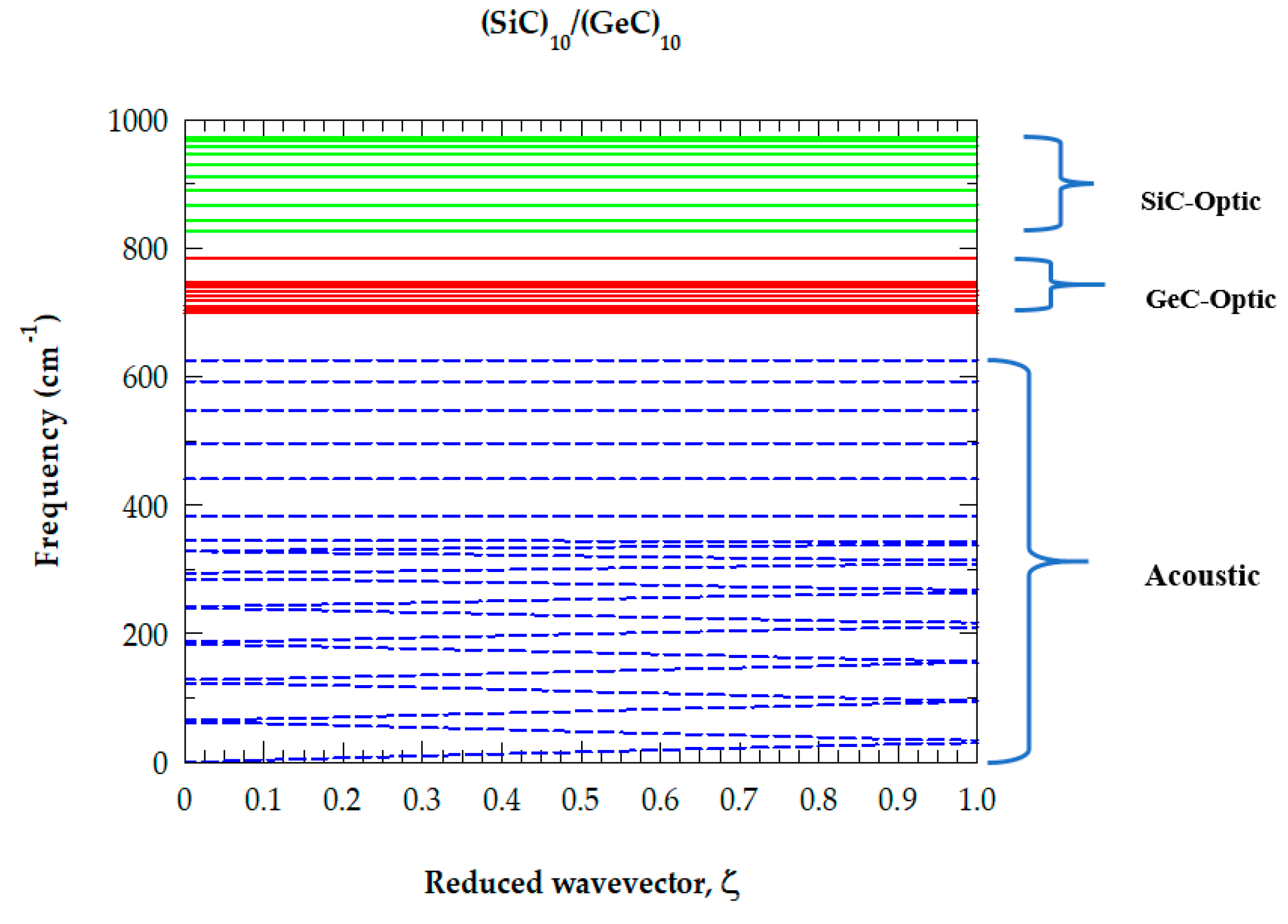
Figure 2.
a) Calculated variation of Raman intensity profiles for (SiC)n/(GeC)10 superlattices by changing SiC-layer thickness n from 2 to 10 (see text). b) Calculated variation of Raman intensity profiles for (SiC)10/(GeC)n superlattices by changing GeC-layer thickness n from 2 to 10 (see text).
Figure 2.
a) Calculated variation of Raman intensity profiles for (SiC)n/(GeC)10 superlattices by changing SiC-layer thickness n from 2 to 10 (see text). b) Calculated variation of Raman intensity profiles for (SiC)10/(GeC)n superlattices by changing GeC-layer thickness n from 2 to 10 (see text).
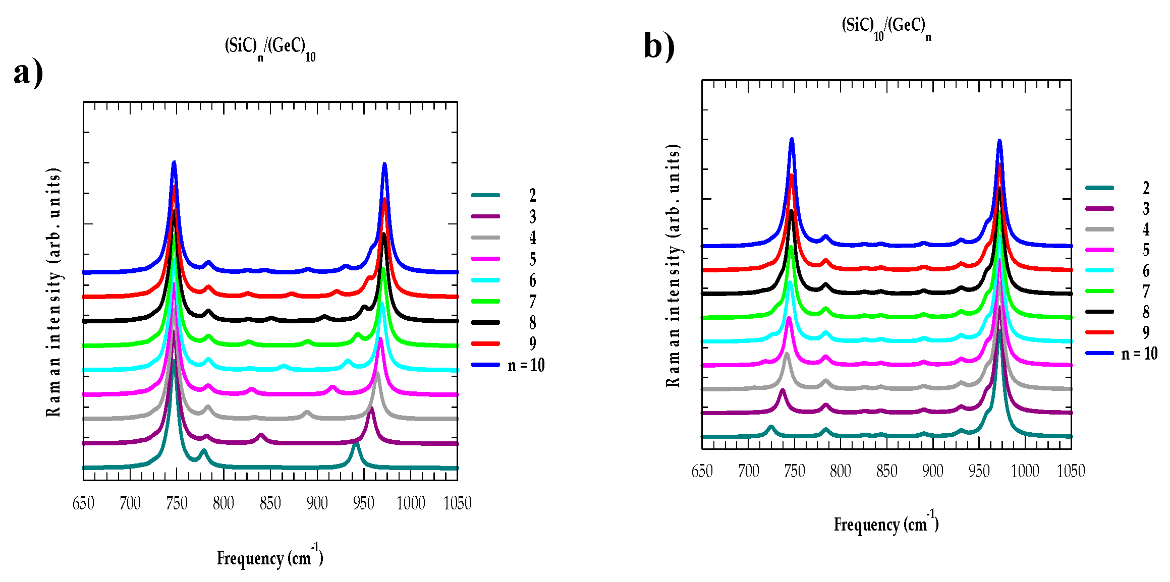
Figure 3.
a) Calculated variation of mode frequencies and their corresponding Raman intensity in graded (SiC)10-Δ/(Si0.5Ge0.5C)Δ/(GeC)10-Δ/(Si0.5Ge0.5C)Δ SL as a function of interfacial layer thickness Δ (≡ 0, 1, 2, 3 MLs) (see text). b) Calculated atomic displacements of selected SiC- and GeC-like optical modes for the graded (SiC)10-Δ/(Si0.5Ge0.5C)Δ/(GeC)10-Δ/(Si0.5Ge0.5C)Δ SL with Δ = 0 and 3. Atomic displacements of Si, C and Ge atoms are indicated by using orange, violet and green colored circles (see: text).
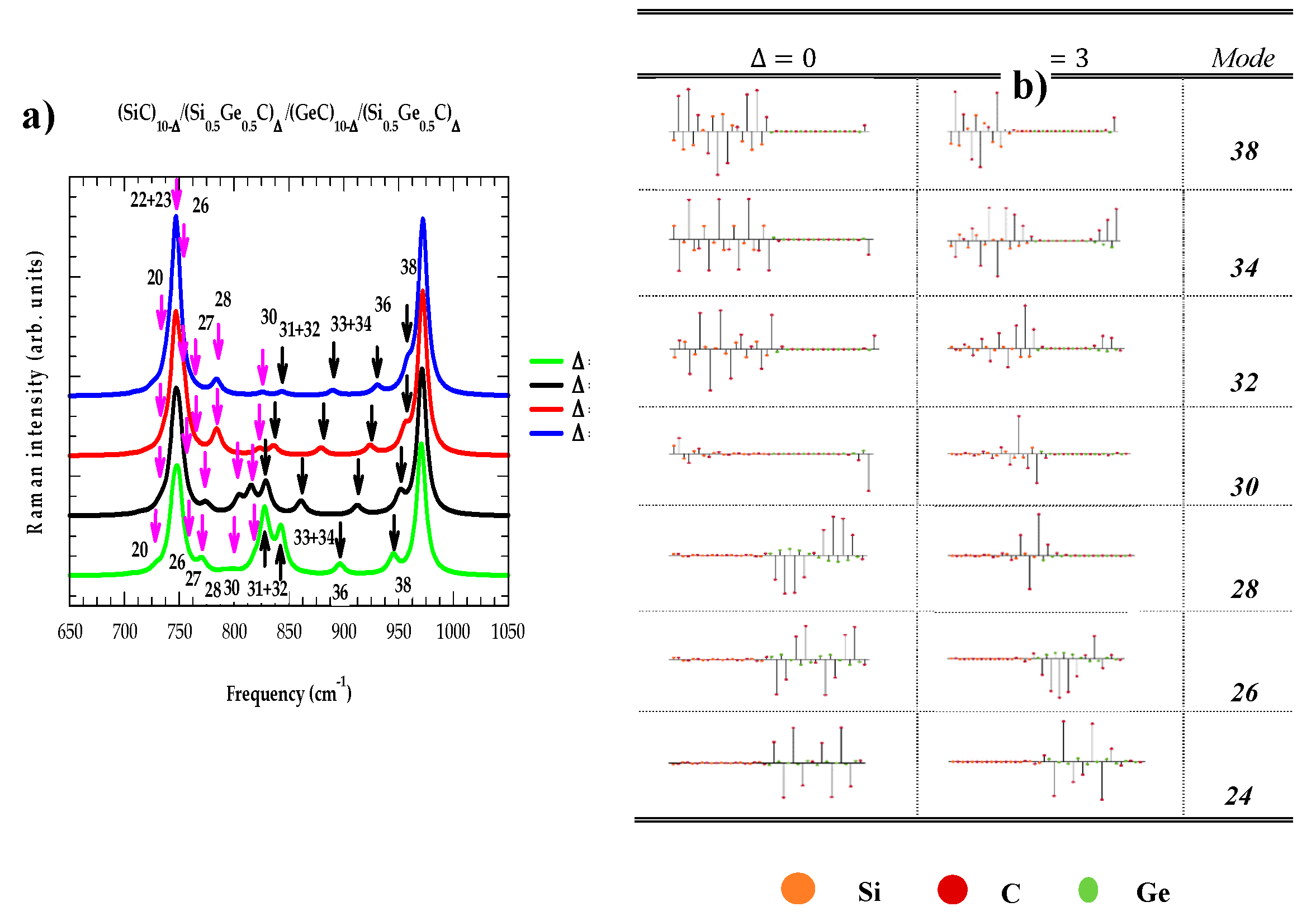
Figure 4.
a) Calculated phonon dispersion curves of SiC (red colored lines) and GeC (blue colored lines) based on rigid-ion model are compared with the existing experimental and theoretical (Table 1) data (see: text). b) Calculated one-phonon density of states of SiC (red colored lines) and GeC (blue colored lines) based on rigid-ion model (see: text).
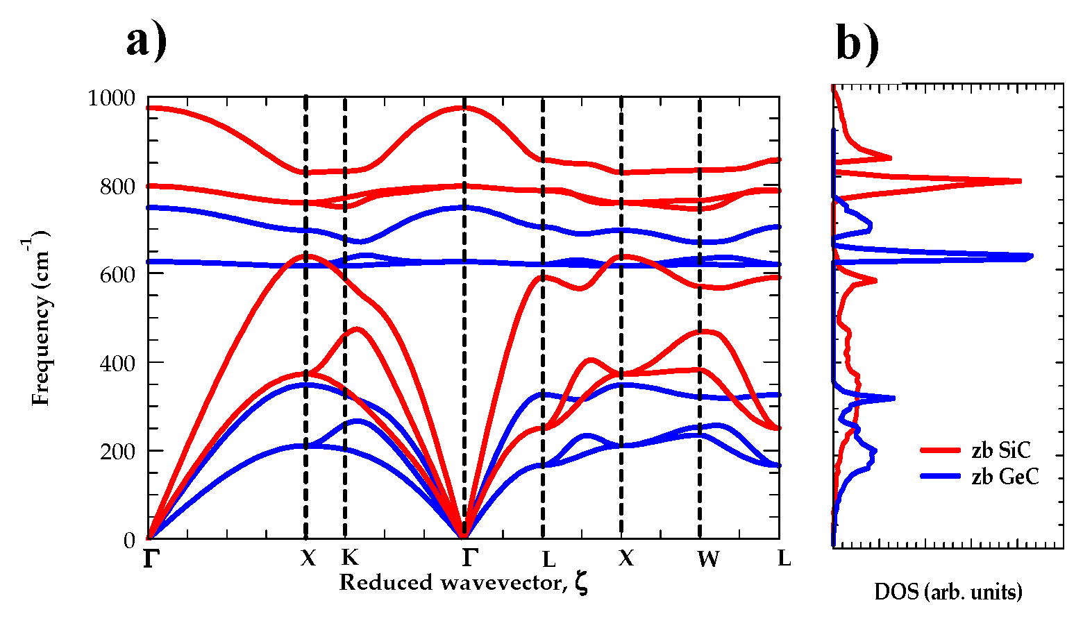
Figure 5.
a) Calculated Debye temperature ΘD as a function of T based on rigid-ion model for SiC- and GeC- compared with experimental and theoretical data Refs. [25,26]. (b) Calculated specific heat Cv (T) as a function of T based on rigid-ion model, compared with experimental and theoretical data [25,26].
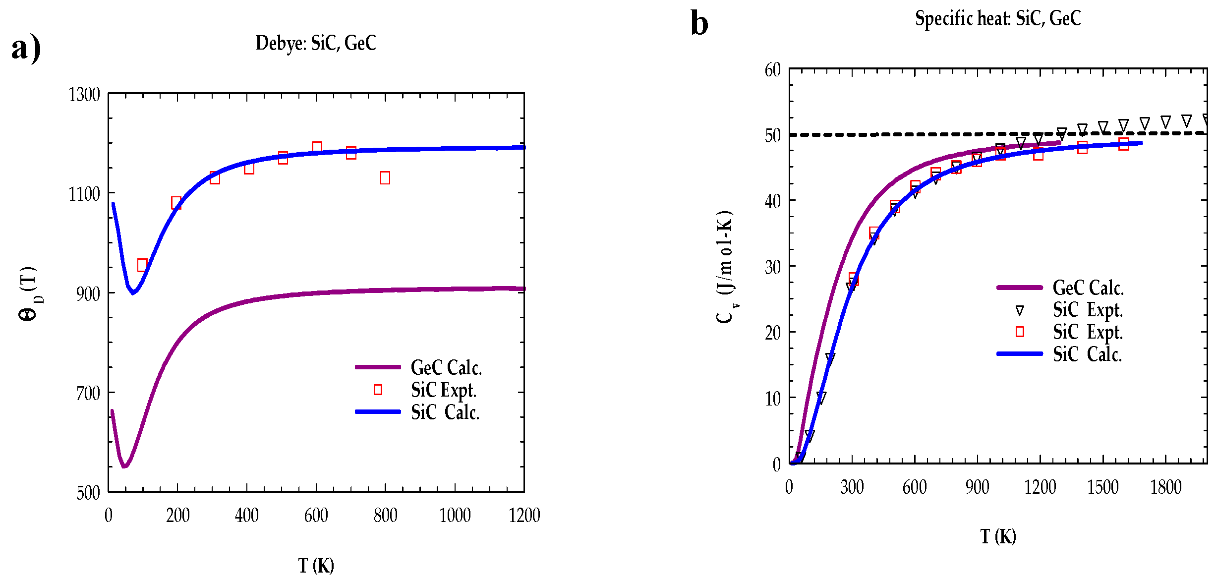
Figure 6.
a) The phonon dispersion curves of (SiC)2/(GeC) 2 superlattice along [001] direction. b) Phonon dispersion curves of SiC along [001] Γ-X direction folded over the same period as that of the superlattice (indicated by vertical black colored dashed lines). c) Phonon dispersion curves of GeC along [001] Γ-X direction folded over the same period as that of the superlattice (indicated by vertical black colored dashed lines).
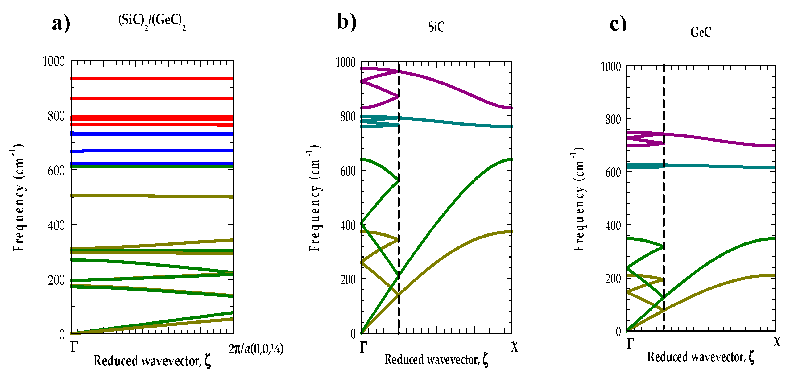
Figure 7.
a) Phonon dispersion curves of (SiC)2/(GeC) 2 superlattice along [110] (left panel) and [100] direction (right panel). b) Complete phonon dispersion curves of (SiC)2/(GeC) 2 superlattice along Γ – X – M – X’– Γ direction in the superlattice Brillouin-zone. c) Frequencies of the zone center ( = 0) optical modes for a (SiC)2/(GeC)2 superlattice as a function of θ (see text).
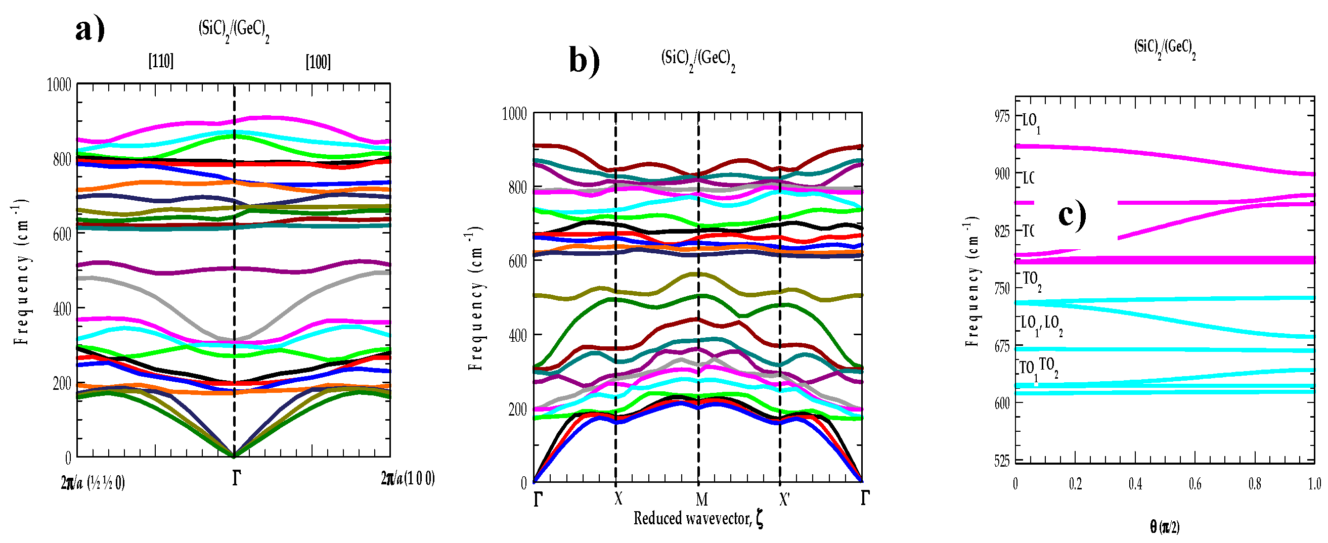

Table 1.
Relevant set of physical parameters for SiC and GaC used in optimizing the rigid-ion-model parameters. The elastic constants c11, c12, and c44 are in 1011 dyn cm−2; lattice constant a0 in (Å) and specific heat Cv in (J/mol-K). The critical-point phonon frequencies are in wave number (cm-1).
| PhysicalParameter Expt. | SiCTheory | GeC Our Theory | Our | ||
|---|---|---|---|---|---|
| c11 c12 c44 a0 LO(Γ) TO(Γ) LO(X) TO(X) LA(X) TA(X) LO(L) TO(L) LA(L) TA(L) |
39.0a) 14.2a) 25.6a) 4.36a) 972b) 796b) 829b) 761b) 640b) 373b) 838b) 766b) 610b) 266b) 1080c) 1270d) 26.84d) |
38.5-39.0e) 13.2-14.2e) 24.3-25.6e) 4.28-4.40e) 945-956e) 774-783e) 807-829e) 741-755e) 622-629e) 361-366e) 817-838e) 747-766e) 601-610e) 257-261e) |
38.7f) 14.3f) 25.8f) 4.36f) 974f) 797f) 828f) 760f) 639f) 373f) 857f) 787f) 591f) 251f) 1080f) 1186f) 26.24f) |
31.8 e) 10.4 e) 19.2 e) 4.59 e) 748 e) 626 e) 697 e) 617 e) 348 e) 214 e) 705 e) 612 e) 331 e) 162 e) |
31.9f) 10.7f) 17.6f) 4.59f) 749f) 626f) 698f) 617f) 348f) 210f) 705f) 621f) 326f) 166f) 670f) 904f) 34.3f) |
Disclaimer/Publisher’s Note: The statements, opinions and data contained in all publications are solely those of the individual author(s) and contributor(s) and not of MDPI and/or the editor(s). MDPI and/or the editor(s) disclaim responsibility for any injury to people or property resulting from any ideas, methods, instructions or products referred to in the content. |
© 2023 by the authors. Licensee MDPI, Basel, Switzerland. This article is an open access article distributed under the terms and conditions of the Creative Commons Attribution (CC BY) license (https://creativecommons.org/licenses/by/4.0/).
Copyright: This open access article is published under a Creative Commons CC BY 4.0 license, which permit the free download, distribution, and reuse, provided that the author and preprint are cited in any reuse.


